

DATA SHEET
MOS INTEGRATED CIRCUIT
µµµµ
PD30121
VR4121
TM
64-/32-BIT MICROPROCESSOR
DESCRIPTION
The µPD30121 (VR4121) is one of NEC’s VR SeriesTM RISC (Reduced Instruction Set Computer) microprocessors
and is a high-performance 64-/32-bit microprocessor employing the MIPS
R
4121 uses the high-performance, super power-saving VR4120TM as the CPU core, and has many peripheral
The V
functions such as a DMA controller, software modem interface, serial interface, keyboard interface, IrDA interface,
touch panel interface, real-time clock, A/D converter, and D/A converter. Configured with these functions, the
R
4121 is suitable for high-speed battery-driven portable information systems. The external memory bus width can
V
be selected from 32 bits and 16 bits, realizing high-speed data transfer.
Detailed function descriptions are provided in the following user’s manual. Be sure to read it before
designing.
R
•
4121 User’s Manual (U13569E)
V
FEATURES
• Employs 64-bit MIPS architecture
• Conforms to MIPS III instruction set (deleting FPU,
LL, LLD, SC, and SCD instructions)
• Optimized 6-stage pipeline • Keyboard interface and touch panel interface
• Supports MIPS16 instruction set • 4-channel DMA controller
• Supports high-speed product-sum operation
instructions
• Supports four types of operating modes, enabling
more effective power-consumption management
• On-chip clock generator
• Address space physical: 32 bits
virtual: 40 bits
Integrates 32 double entry TLBs
• High-capacity instruction/data separated cache
memories
Instruction: 16 Kbytes
Data: 8 Kbytes
• Memory controller (ROM, EDO-type DRAM,
synchronous DRAM (SDRAM), synchronous ROM
(SROM), and flash memory supported)
• Serial interface (NS16550 compatible)
• IrDA interface for infrared communication
• Software modem interface
• A/D and D/A converters to support digital voice I/O
• Supports ISA bus subset• Internal maximum operating frequency: 131/168 MHz
• Power supply voltage: V
3.3 V (external) (131 MHz model)
• Package: 224-pin fine-pitch FBGA
TM
RISC architecture.
DD
2 = 2.5 V (internal), VDD3 =
APPLICATIONS
Battery-driven portable information systems
•
Embedded controllers, etc.
•
ORDERING INFORMATION
Part Number Package Internal Maximum Operating Frequency
PD30121F1-131-GA1 224-pin plastic FBGA (16 × 16) 131 MHz
µ
PD30121F1-168-GA1 224-pin plastic FBGA (16 × 16) 168 MHz
µ
The information in this document is subject to change without notice. Before using this document, please
confirm that this is the latest version.
Not all devices/types available in every country. Please check with local NEC representative for
availability and additional information.
Document No. U14691EJ1V0DS00 (1st edition)
Date Published June 2000 N CP(K)
Printed in Japan
2000©
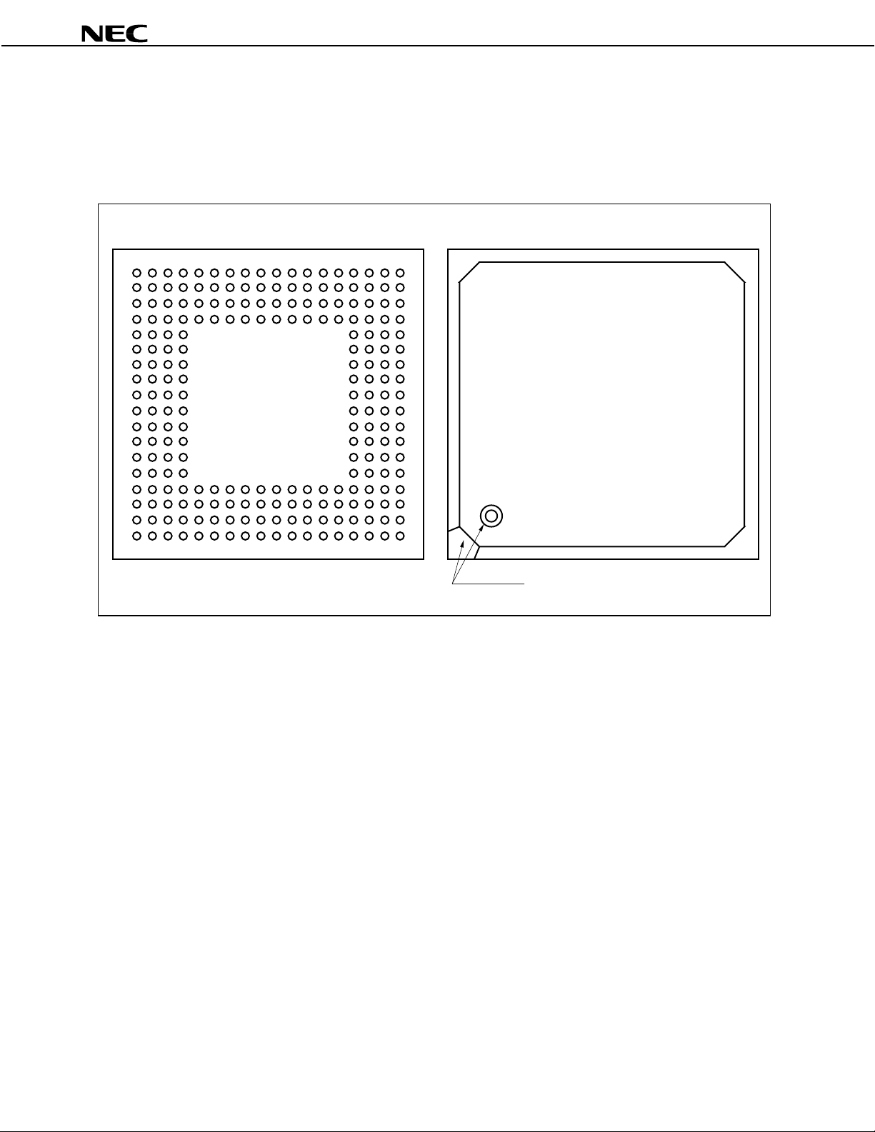
PIN CONFIGURATION
224-pin plastic FBGA (16 × 16)
•
PD30121F1-131-GA1
µ
PD30121F1-168-GA1
µ
Bottom view Top view
18
17
16
15
14
13
12
11
10
9
8
7
6
5
4
3
2
1
µµµµ
PD30121
VUTRPNMLKJHGFEDCBA ABCDEFGHJKLMNPRTUV
Index mark
2
Data Sheet U14691EJ1V0DS00
µµµµ
PD30121
Pin No. Power
Supply
A1 3.3 V VDD3 C15 3.3 V RTS#/CLKSEL1 H15 3.3 V GND3
A2 3.3 V SHB# C16 3.3 V GND3 H16 3.3 V KPORT6
A3 3.3 V BUSCLK C17 3.3 V ILCSENSE H17 3.3 V KPORT4
A4 3.3 V HLDACK# C18 3.3 V AFERST# H18 2.5 V VDD2
A5 3.3 V IOCHRDY D1 3.3 V DATA5 J1 3.3 V DATA20/GPIO20
A6 3.3 V MEMW# D2 3.3 V DATA3 J2 3.3 V DATA17/GPlO17
A7 3.3 V ADD23 D3 3.3 V DATA6 J3 3.3 V DAT A 22/GPlO22
A8 3.3 V VDD3 D4 3.3 V GND3 J4 3.3 V DATA19/GPIO19
A9 3.3 V ADD18 D5 3.3 V MEMCS16# J15 3.3 V KSCAN9/GPIO41
A10 3.3 V ADD15 D6 3.3 V ADD25/SCLK J16 3.3 V VDD3
A11 3.3 V ADD8 D7 3.3 V GND3 J17 2. 5 V GND2
A12 3.3 V ADD7 D8 3.3 V ADD19 J18 3.3 V KSCAN11/ GPIO43
A13 2.5 V VDD2 D9 3.3 V ADD16 K1 3.3 V DATA23/GPIO23
A14 3.3 V DCD#/GPIO15 D10 3.3 V ADD14 K2 3.3 V DATA26/GPI O26
A15 3.3 V TXD/CLKSEL2 D11 3.3 V VDD3 K3 3.3 V DATA25/GPIO25
A16 3.3 V IRDOUT# D12 3.3 V GND3 K4 3.3 V DATA21/GPIO21
A17 3.3 V IRING D13 3.3 V ADD4 K15 3.3 V KSCAN7/GPIO39
A18 3.3 V VDD3 D14 3.3 V CTS# K16 3.3 V KSCAN10/GP IO42
B1 3.3 V DATA1 D15 3.3 V GND3 K17 3.3 V KSCAN5/GPIO37
B2 3.3 V IOR# D16 3.3 V GND3 K18 3.3 V KSCAN8/GPIO40
B3 3.3 V IOW# D17 3. 3 V SDI L1 3.3 V DAT A 27/GPIO27
B4 3.3 V LEDOUT# D18 3.3 V SDO L2 3.3 V DAT A31/GPIO31
B5 3.3 V FIRCLK E1 3.3 V DATA9 L3 3.3 V DATA29/GPIO29
B6 3.3 V HLDRQ# E2 3.3 V DATA4 L4 3.3 V DAT A 24/GPIO24
B7 3.3 V ZWS# E3 3.3 V DATA7 L15 3.3 V KSCAN3/ GP IO35
B8 3.3 V ADD24 E4 3.3 V DATA10 L16 3.3 V KSCAN6/GPIO38
B9 3.3 V ADD21 E15 3.3 V OPD# L17 3.3 V KSCAN0/GPIO32
B10 3.3 V ADD12 E16 3.3 V HSPSCLK L18 3.3 V KSCAN4/GPIO36
B11 3.3 V ADD6 E17 3.3 V FS M1 3.3 V DATA30/GPIO30
B12 2.5 V GND2 E18 3.3 V HC0 M2 3.3 V VDD3
B13 3.3 V DSR# F1 3.3 V DATA13 M3 3.3 V GND3
B14 3.3 V IRDIN F2 3.3 V DATA8 M4 3.3 V DATA28/GPIO28
B15 3.3 V FIRDIN#/SEL F3 3.3 V DATA11 M15 3.3 V KSCAN2/GPIO34
B16 3.3 V BATTINH/BATTINT# F4 3.3 V DATA14 M16 3.3 V MIPS16EN
B17 3.3 V OFFHOOK F15 3.3 V KPORT3 M17 3.3 V GND3
B18 3.3 V MUTE F16 3.3 V HSPMCLK M18 3.3 V KSCAN1/GPIO 33
C1 3.3 V DATA2 F17 3.3 V TELCON N1 2.5 V VDD2
C2 3.3 V DATA0 F18 3.3 V KPORT1 N2 3.3 V ADD3
C3 3.3 V SM ODE2 G1 2. 5 V VDD2 N3 3.3 V ADD10
C4 3.3 V CKE G2 3.3 V DATA12 N4 3.3 V GND2
C5 3.3 V GND3 G3 3.3 V DATA15 N15 3.3 V GND3
C6 3.3 V IOCS16# G4 3.3 V GND3 N16 3.3 V VDD3
C7 3.3 V MEM R# G15 3. 3 V KPORT7 N17 2.5 V VDDP
C8 3.3 V ADD22 G16 3.3 V KPORT2 N18 3.3 V GND3
C9 3.3 V ADD20 G17 3.3 V KPORT0 P1 3.3 V ADD9
C10 3.3 V ADD17 G18 3.3 V KPORT5 P2 3.3 V ADD0
C11 3.3 V ADD13 H1 3.3 V DATA16/GP IO16 P3 3.3 V A DD2
C12 3.3 V ADD5 H2 2.5 V GND2 P4 3.3 V ADD11
C13 3.3 V RXD H3 3.3 V DATA18/GPIO18 P15 2.5 V VDD2 (VDDPD)
C14 3.3 V DTR#/CLKSEL0 H4 3.3 V VDD3 P16 2.5 V GNDP
Pin Name Pin No. Power
Supply
Pin Name Pin No. Power
Supply
Pin Name
Remark
# indicates active low.
Data Sheet U14691EJ1V0DS00
3
µµµµ
PD30121
Pin No. Power
Supply
P17 3.3 V CLKX2 T6 3.3 V AV
P18 2.5 V GND2 (GNDPD) T7 3.3 V LCAS# U14 3.3 V SYSDIR/GPIO6
R1 3.3 V ADD1 T8 3.3 V ROMCS2# U15 3.3 V SCAS#/GPI O5
R2 3.3 V POWER T9 3.3 V RD# U16 3.3 V GPIO1
R3 3.3 V GND3 T10 3.3 V WR# U17 3.3 V GPIO2
R4 3.3 V GND3 T11 3.3 V DBUS 32/GPIO48 U18 3.3 V CGND
R5 3.3 V AUDIOIN T12 3.3 V DDOUT/GPI O44 V1 3.3 V VDD3
R6 3.3 V DV
R7 3.3 V MRAS2#/ULCAS# T14 3.3 V GPIO8 V3 3.3 V TPX0
R8 3.3 V MRA S 1# T15 3.3 V GND3 V4 3.3 V TPY1
R9 3.3 V ROMCS1# T16 3.3 V GND3 V5 3.3 V ADIN2
R10 3.3 V RSTOUT T17 3.3 V GPIO0 V6 3.3 V AUDIOOUT
R11 3.3 V GND3 T18 3.3 V RTCX 1 V7 3.3 V MRAS 3#/UUCAS#
R12 3.3 V SMODE1/GP IO49 U1 3.3 V MPOWER V8 3.3 V MRAS0#
R13 3.3 V DDIN/GPIO45 U2 3.3 V RTCRST# V9 3.3 V ROMCS0#
R14 3.3 V GPIO12 U3 3.3 V AGND V10 3.3 V VDD3
R15 3.3 V GND3 U4 3. 3 V TP X 1 V11 3 . 3 V LCDCS#
R16 3.3 V CV
R17 3.3 V RTCX2 U6 3.3 V ADIN1 V13 3 . 3 V GPIO14
R18 3.3 V CLKX1 U7 3.3 V DGND V14 3.3 V GPI O10
T1 3.3 V POWERON U8 3.3 V UCAS# V15 3.3 V SPOWER/GPIO7
T2 3.3 V RSTSW# U9 3.3 V ROMCS3# V16 3.3 V SRAS#/GPIO4
T3 3.3 V GND3 U10 3.3 V LDCRDY V 17 3.3 V GPI O3
T4 3.3 V PIUV
T5 3.3 V ADIN0 U12 3.3 V GPIO13
Pin Name Pin No. Power
DD
DD
DD
T13 3.3 V GPIO11 V2 3.3 V PIUGND
U5 3.3 V TPY0 V12 3.3 V DCTS#/GPIO47
U11 3.3 V DRTS#/GPIO46 V18 3.3 V VDD3
Supply
Pin Name Pin No. Power
DD
U13 3.3 V GPIO9
Pin Name
Supply
Remark
# indicates active low.
4
Data Sheet U14691EJ1V0DS00

µµµµ
PD30121
PIN IDENTIFICATION
ADD (0:25): Address Bus LCDCS#: LCD Chip Select
ADIN (0:2): General Purpose Input for A/D LCDRDY: L CD Ready
AFERST#: AFE Reset LEDOUT#: LED Output
AGND: GND for A/D MEMCS16#: Memory Chip Select 16
AUDIOIN: Audio Input MEMR#: Memory Read
AUDIOOUT: Audio Output MEMW#: Memory Write
DD
AV
:V
BATTINH: Battery Inhibit MPOWER: Main Power
BATTINT#: Battery Interrupt Request MRAS(0:3)#: DRAM Row Address Strobe
BUSCLK: System Bus Clock MUTE: Mute
CGND: GND for Oscillator OFFHOOK: Off Hook
CKE: Clock Enable OPD#: Output Power Down
CLKSEL (0:2): Clock Select PIUGND: GND for Touch Panel Interface
CLKX1: Clock X1 PIUV
CLKX2: Clock X2 POWER: Power Switch
CTS#: Clear to Send POWERON: Power On State
DD
CV
:V
DATA (0:31): Data Bus ROMCS(0:3)#: ROM Chip Select
DBUS32: Data Bus 32 RSTOUT: System Bus Reset Output
DCD#: Data Carrier Dete ct RSTSW#: Reset Switch
DCTS#: Debug Serial Clear to Send RTCRST#: Real-time Clock Reset
DDIN: Debug Serial Data Input RTCX1: Real-time Clock X1
DDOUT: Debug Serial Data Output RTCX2: Real-time Clock X2
DGND: GND for D/A RTS#: Request to Send
DRTS#: Debug Serial Request to Send RxD: Receive Data
DSR#: Data Set Ready SCAS#:
DTR#: Data Terminal Ready
DVDD
:V
FIRCLK: FIR Clock SDI: HSP Serial Data Input
FIRDIN#: FIR Data Input SDO: HSP Serial Data Output
FS: Frame Synchronization SEL: IrDA Module Select
GND2, GND3: Ground SHB#: System Hi-Byte Enable
GNDP, GNDPD: Ground for PLL SMODE (1:2): SDRAM Mode
GPIO (0:49): General Purpose I/O SPOWER: SDRAM Power Control
HC0: Hardware Control 0 SRAS#:
HLDACK#: Hold Acknowledge
HLDRQ#: Hold Request SYSDIR: System Bus Buffer Direction
HSPMCLK: HSP Codec Master Clock TELCON: Telephone Control
HSPSCLK: HSP Codec Serial Clock TPX (0:1): Touch Panel X I/O
ILCSENSE: Input Loop Current Sensing TPY (0:1): Touch Panel Y I/O
IOCHRDY: I/O Channel Ready TxD: Transmit Data
IOCS16#: I/O Chip Select 16 UCAS#: Upper Column Address Strobe
IOR#: I/O Read ULCAS#: Lower Byte of Upper Column
IOW#: I/O Write Address Strobe
IRDIN: IrDA Data Input UUCAS#: Upper Byte of Upper Column
IRDOUT#: IrDA Data Output Address Strobe
IRING: Input Ring V
KPORT (0:7): Key Code Data Input V
KSCAN (0:11): Key Scan Line WR#: Write
LCAS#: Lower Column Address Strobe ZWS#: Zero Wait State
DD
for A/D MIPS16EN: MIPS16 Enable
DD
:V
DD
for Oscillator RD#: Read
DD
for Touch Panel Interface
Column Address Strobe for
SDRAM/SROM
DD
for D/A SCLK: SDRAM/SROM Clock
Row Address Strobe for
SDRAM/SROM
DD
2, VDD3: Power Supply Voltage
DD
P, VDDPD: VDD for PLL
Remark
# indicates active low.
Data Sheet U14691EJ1V0DS00
5
µµµµ
INTERNAL BLOCK DIAGRAM AND EXAMPLE OF CONNECTION OF EXTERNAL BLOCKS
32.768 kHz 18.432 MHz
CODEC AFE
PD30121
OSB OSB PLL
LCD module
PD16661
µ
LCD panel
480 × 240
PC card
ROM/SROM/flash
memory
EDO DRAM/
SDRAM
µ
PD16666
PCMCIA
/buffer
VR4120 CPU core
131/168 MHz
BCU
VR4121
CPU CORE INTERNAL BLOCK DIAGRAM
Virtual address bus
Internal data
bus
HSP
RTC
DSU
ICU
PMU
CMU
DCU
DMAAU
GIU
KIU
LED
AIU
PIU
SIU
FIR
48 MHz
D/A
A/D
Touch panel
RS-232C
driver
IR
driver
Address/data (o)
Address/data (i)
6
Control (o)
Control (i)
Internal clock
Bus
interface
Data
cache
(8 Kbytes)
Data Sheet U14691EJ1V0DS00
Instruction
cache
(16 Kbytes)
Clock
generator
CP0 CPU
TLB

µµµµ
PD30121
CONTENTS
1. PIN FUNCTIONS.................................................................................................................................. 8
1.1 Pin Functions .............................................................................................................................................8
1.2 Pin Status in Specific Status...................................................................................................................17
1.3 Recommended Connection and I/O Circuit Types................................................................................21
1.4 Pin I/O Circuits .........................................................................................................................................24
2. ELECTRICAL SPECIFICATIONS...................................................................................................... 25
3. PACKAGE DRAWING....................................................................................................................... 71
4. RECOMMENDED SOLERING CONDITIONS .................................................................................. 72
Data Sheet U14691EJ1V0DS00
7
1. PIN FUNCTIONS
µµµµ
PD30121
Remark
# indicates active low.
1.1 Pin Functions
(1) System bus interface signals
Signal I/O Function
ADD25/SCLK O This function diff ers depending on how the SMODE (1:2) signal is set.
<When SMODE (1:2) signal = 00>
This is a 25-bit address bus .
<When SMODE (1:2) signal ≠ 00>
This is the operating cloc k for SDRAM and SROM.
ADD (0:24) O This is a 25-bit address bus. The VR4121 uses this to specify addresses for the SDRAM, SROM,
DRAM, ROM, LCD, or system bus (ISA).
DATA (0:15) I/O This is a 16-bi t dat a bus . The VR4121 uses this to transm it and receive data with a SDRAM , SROM,
DRAM, ROM, LCD, or system bus.
DATA (16:31)/
GPIO (16:31)
LCDCS# O This is the LCD chip sel ect signal. This s ignal is active when the VR4121 is performing LCD acces s and
RD# O This i s active when the VR4121 is reading data from the LCD, SDRA M , SROM, DRAM, or ROM.
WR# O This is active when the VR4121 is writing data to the LCD, SDRAM, or DRAM.
LCDRDY I This is the LCD ready signal. Set this signal as active when the LCD controller is ready to recei ve
ROMCS (2:3)# O The function differs wi th the setting of the DBUS32 signal.
ROMCS (0:1)# O This i s the ROM or SROM chip select signal.
CKE O This is the SDRAM or SROM c lock enable signal. When using neither SDRAM nor SROM, c onnect to
UUCAS#/
MRAS3#
I/O This function differs depending on how the DBUS32 signal is s et .
<When DBUS32 signal = 1>
This is the high-order 16 bits of the 32-bit data bus.
R
This bus is used for trans m i tting and receiving data between the V
<When DBUS32 signal = 0>
This is a general-purpose I/O port .
high-speed system bus access using the ADD/DATA bus.
access from the V
<When DBUS32 signal = 1>
This becomes the chip s el ect signal for the extended ROM, SROM, DRAM, or SDRAM.
<When DBUS32 signal = 0>
This is the ROM or SROM chip sel ec t signal.
GND or leave open.
O This functi on di ffers depending on how the DBUS32 signal i s set or types of memory to be accessed.
<When DBUS32 signal = 1>
When accessing DRAM (EDO t ype): This signal is active (UUCAS#) when a valid column address is
output via the ADD bus during ac cess of DATA (24:31) in the 32-bit data bus.
When accessing SDRAM: T hi s is the I/O buffer cont rol signal (UUDQM#) that is used during ac cess
of DATA (24:31) signal in the 32 bi t data bus.
During 32-bit access of LCD/ hi gh-speed system memory: Byte enable signal that is used during
access of DATA (24:31) signal.
<When DBUS32 signal = 0>
When accessing DRAM (EDO t ype): This is the DRAM's RAS signal (MRAS3#). This signal is
active when a valid row address i s output via the ADD bus for the DRA M connected to the high-order
address.
When accessing SDRAM: Thi s is the SDRAM's chi p select signal (CS3#). This signal is active when
a command is issued for the SDRAM connected to the high-order address.
R
4121.
4121 and the DRAM and ROM.
(1/3)
8
Data Sheet U14691EJ1V0DS00
µµµµ
PD30121
Signal I/O Function
ULCAS#/
MRAS2#
MRAS (0:1)# O This function diff ers depending on the type of memory being accessed.
UCAS# O This functi on di f fers depending on the type of memory bei ng accessed.
LCAS# O This function differs depending on the ty pe of memory being accessed.
BUSCLK O This is the system bus clock. It is used to output the clock that is supplied to the controller on the
SHB# O This is the system bus high-byte enable signal. During 16-bit system bus access, this signal is active
IOR# O This is the system bus I/O read signal. It is active when the VR4121 accesses the system bus to read
IOW# O This is the system bus I/O write signal. It is active when the VR4121 accesses the system bus to write
MEMR# O This is the system bus memory read signal. It is active when the VR4121 accesses the system bus to
MEMW# O This is the system bus memory write signal. It is active when the VR4121 accesses the system bus to
ZWS# I This is the system bus zero wait state signal. Set this signal as acti ve to enable the controller on the
O This functi on di ffers depending on how the DBUS32 signal i s set and type of memory being ac cessed.
<When DBUS32 signal = 1>
When accessing DRAM (EDO t ype): This signal is act i ve (ULCAS#) when a valid column address i s
output via the ADD bus during ac cess of DATA (16:23) signal i n the 32-bit data bus.
When accessing SRAM: Thi s i s the I/O buffer control signal (ULDQM#) that is used during ac cess of
DATA (16:23) signal in the 32-bit dat a bus.
During 32-bit access of LCD/ hi gh-speed system memory: Byte enable signal that is used during
access of DATA (16:23) signal.
<When DBUS32 signal = 0>
When accessing DRAM (EDO t ype): This is the DRAM's RAS signal (MRAS2#). This signal is
active when a valid row address i s output via the ADD bus for the DRA M connected to the next
highest address after the hi ghest high-order address.
When accessing SDRAM: Thi s is the SDRAM's chi p select signal (CS2#). This signal is active when
a command is issued for the SDRAM connected to the s econd highest high-order address.
<When accessing DRAM (EDO t ype)>
This is the DRAM's RA S-only signal.
<When accessing SDRAM>
This is the SDRAM's chip select signal (CS (0: 1)#).
<When accessing DRAM (EDO t ype)>
This is the DRAM's CA S signal. This signal is active when a valid column addres s is output via the
ADD bus during access of DATA (8:15) signal in the DRAM.
<When accessing SDRAM>
This is the I/O buff er control signal (UDQM#) that is used during access of DATA (8:15) signal.
< During 32-bit access of LCD/ hi gh-speed system memory >
This is the byte enable si gnal that is used during access of DATA (8:15) signal. This signal is active
when a valid address is output via the ADD bus for access to DATA (8:15) signal when the si ze of
the access bus to t he LCD i s 32 bits.
<When accessing DRAM (EDO t ype)>
This is the DRAM's CA S signal. This signal is active when a valid column addres s is output via the
ADD bus during access of DATA (0:7) signal in the DRAM.
<When accessing SDRAM>
This is the I/O buff er control signal (LDQM#) that is used during access of DATA (0:7) signal.
< During 32-bit access of LCD/ hi gh-speed system memory >
This is the byte enable si gnal that is used during access of DATA (0:7) signal.
system bus. Its frequency is determined based on the status of the CLKSEL (0:2) signal. Ordinarily,
the frequency is 1/4 of t he TCl ock frequency. (See
can be changed via the PMU register settings.
when the high-order byte is valid on t he data bus.
data from an I/O port.
data to an I/O port.
read data from memory.
write data to memory.
system bus to be accessed by the V
R
4121 without a wait interval.
(5) RS-232C interface signals
). The frequency
(2/3)
Data Sheet U14691EJ1V0DS00
9
µµµµ
PD30121
(3/3)
Signal I/O Function
RSTOUT O This is the system bus reset signal. It is active when the VR4121 resets the system bus controller
(during bus timeout, manipulation of BCUCNTREG1 register, and power-down mode).
MEMCS16# I Thi s i s a dynamic bus sizing request signal. Set this signal as active when system bus memory
accesses data in 16-bit wi dth. This signal is inv al i d when 32-bi t wi dth is selected using LCD/hi gh-speed
system bus.
IOCS16# I This is a dynamic bus s i zing request signal. Set t hi s signal as active when system bus I/O accesses
data in 16-bit width. This s i gnal i s invalid when 32-bit width is s el ected using LCD/high-speed system
bus.
IOCHRDY I This is the system bus ready signal. Set this signal as active when the system bus controller is ready to
be accessed by the V
HLDRQ# I This is a hold request signal for the system bus and DRAM bus that is s ent from an external bus mast er.
HLDACK# O This is a hol d ac knowledge signal for the system bus and DRAM bus that is s ent to an external bus
master.
SRAS#/GPIO4 I/O This function differs depending on the type of memory being access ed.
<When accessing DRAM (EDO t ype)>
This is a general-purpose I/O port .
<When accessing SDRAM>
This is the RAS signal for SDRAM and SROM only.
SCAS#/GPIO5 I/O This function differs depending on the type of memory being access ed.
<When accessing DRAM (EDO t ype)>
This is a general-purpose I/O port .
<When accessing SDRAM>
This is the CAS signal for SDRAM and SROM only.
SYSDIR/GPIO6 I/O This function differs depending on t he type of memory being accessed.
<When accessing DRAM (EDO t ype)>
This is a general-purpose I/O port .
<When accessing SDRAM>
This is the direction c ontrol signal for the buffer used to reduce the DATA bus's load.
SPOWER/
GPIO7
I/O This function differs depending on the type of memory being ac cessed.
<When accessing DRAM (EDO t ype)>
This is a general-purpose I/O port .
<When accessing SDRAM>
This is the SDRAM's power supply control signal.
R
4121.
(2) Clock interface signals
Signal I/O Function
RTCX1 I This is t he 32.768-kHz oscillator’s input pin. It is connected to one side of a cry stal resonator.
RTCX2 O This is the 32.768-kHz oscillator’s output pin. It is connected t o one s i de of a crystal resonator.
CLKX1 I This is the 18.432-MHz oscillator’s input pin. It is connected to one side of a cry stal resonator.
CLKX2 O This is the 18.432-MHz oscillator’s output pin. It is connected t o one s i de of a crystal resonator.
FIRCLK I This is the 48-MHz clock input pi n. Fix this at high level when FIR is not used.
10
Data Sheet U14691EJ1V0DS00
µµµµ
PD30121
(3) Battery monitor interface signals
Signal I/O Function
BATTINH/
BATTINT#
I This functi on di ffers depending on how the MPOWER signal i s set.
<When MPOWER signal = 0>
BATTINH function
This signal enables/prohibits activation due to power-on.
1 : Enable activation
0 : Prohibit activat i on
<When MPOWER signal = 1>
BATTINT# function
This is an interrupt signal t hat is output when remaining power is low duri ng norm al operations. The
external agent checks the remaining battery power. Activate the signal at this pin if v ol tage sufficient
for operations cannot be supplied.
(4) Initialization interface signals
Signal I/O Function
MPOWER O T hi s signal indicates the VR4121 is operating. This signal i s i nactive during Hibernate mode.
POWERON O This signal i ndi c ates the VR4121 is ready to operate. It becomes active when a power-on fact or i s
detected and becomes inact i ve when the BATTINH/BATTINT# s i gnal check operation is completed.
POWER I This is a VR4121 activation signal.
RSTSW# I This is a VR4121 reset signal.
RTCRST# I T hi s signal resets RTC. When power is first supplied to a device, the external agent must as sert the
signal at this pin for about 2 s.
Data Sheet U14691EJ1V0DS00
11
µµµµ
PD30121
(5) RS-232C interface signals
Signal I/O Function
RxD I This is a rec ei ve data signal. It is used when the RS-232C controller sends s eri al data to the VR4121.
CTS# I This is a transmit enable signal. Assert this signal when the RS-232C controller is ready to receive
transmission of seri al data.
DCD#/
GPIO15
DSR# I This is the data set ready signal. Ass ert this signal when the RS-232C cont rol l er i s ready to
TxD/
CLKSEL2,
RTS#/
CLKSEL1,
DTR#/
CLKSEL0
I This is a carri er det ection signal. Assert this signal when valid s eri al dat a i s being received. It is al so
R
used when detecting a power-on factor for the V
4121.
When this pin is not used for DCD# signal, this pin can be used as an i nterrupt detection functi on for the
GIU unit.
R
receive/transmit serial data between the controller and t he V
4121.
I/O This function differs depending on the operating status.
<During normal operation (output)>
Signals used for serial c om munication
TxD signal :
R
This is a transmit dat a signal. It is used when the V
4121 sends serial data to the RS -232C
controller.
RTS# signal :
R
This is a transmit reques t signal. This signal is asserted when the V
4121 is ready to receive seri al
data from the RS-232C controller.
DTR# signal :
R
This is a terminal equipment ready signal. This signal is asserted when the V
4121 is ready to
transmit or receive seri al data.
<When RTC reset (input)>
Signals (CLKSEL (2:0) signal) used to set the CPU core operation frequency, BUSCLK si gnal
frequency, and internal bus c l ock frequency. These signal s are sampled when the RTCRST# signal
changes from low level to hi gh l ev el .
The relationships between the
CLKSEL (2:0) signal setting and each cl ock frequency are shown below.
Notes 1.
12
CLKSEL
(2:0)
signal
Note 1
111
Note 2
110
Note 2
101
CPU core
operation
frequency
(PClock)
RFU RFU RFU RFU RFU RFU
168.5 MHz 28.1 MHz 56.2 MHz 28.1 MHz 7.0 MHz 7.0 MHz
147.5 MHz 29.5 MHz 59.0 MHz 29.5 MHz 7.4 MHz 7.4 MHz
SDRAM/SROM
operation frequency
(VTClock)
MIN. MAX.
BUSCLK
signal
frequency
(When
TClock
output)
BUSCLK
signal
requency
(When 1/4
of TClock)
Interrupt
control
clock
frequency
(MasterOut)
100 131.1 MHz 32.8 MHz 65.5 MHz 32. 8 M Hz 8. 2 M Hz 8.2 MHz
011 118.0 MHz 29.5 MHz 59.0 MHz 29. 5 M Hz 7. 4 M Hz 7.4 MHz
010 98.3 MHz 32.8 MHz 65.5 MHz 32.8 MHz 8.2 MHz 8.2 MHz
001 90.7 MHz 30.2 MHz 60.5 MHz 30.2 MHz 7.6 MHz 7.6 MHz
000 78.6 MHz 26.2 MHz 52.4 MHz 26.2 MHz 6.6 MHz 6.6 MHz
Do not set CLKSEL (2:0) = 111.
The settings CLKSEL (2:0) = 110 and 101 are only guaranteed for the 168 MHz model. Do not apply
2.
these settings to the 131 MHz model.
Data Sheet U14691EJ1V0DS00
µµµµ
PD30121
(6) IrDA interface signals
Signal I/O Function
IRDIN I This is an IrDA serial data input signal. It is used when the VR4121 sends serial data to the I rDA
controller, for both FIR and SIR. If the IrDA control l er used is an HP product, however, t hi s signal should
be used for only SIR.
FIRDIN#/SEL I/O This function differs according to the IrDA controller used.
<HP’s controller>
FIRDIN#: It is an FIR rec ei ve data input signal.
<TEMIC’s controller>
SEL: It is an output port for external FIR/SIR s witching.
<SHARP’s controller>
Use is prohibited.
IRDOUT# O This is the IrDA serial dat a output signal. It is us ed when the IrDA controller sends s eri al data from the
R
4121.
V
(7) Debug serial interface signals
Signal I/O Function
DDOUT/
GPIO44
DDIN/
GPIO45
DRTS#/
GPIO46
DCTS#/
GPIO47
O This is the debug serial data output signal. It is used when the VR4121 sends serial data to an ext ernal
debug serial controller.
When this pin is not used for the DDOUT signal, it can be used as a general -purpose output port.
I/O This is the debug serial data i nput signal. It is used when an external debug serial data controller s ends
R
serial data to the V
When this pin is not used for the DDIN signal, it can be used as a general-purpose output port.
O This is a transmission request s i gnal . The VR4121 asserts this si gnal before sending serial data.
When this pin is not used for the DRTS# signal, it can be used as a general-purpose output port.
I/O This is a transmit ac knowledge signal. The VR4121 asserts this si gnal when i t is ready to receive
transmitted serial dat a.
When this pin is not used for the DCTS# signal, it can be used as a general-purpose output port.
4121.
(8) Keyboard interface signals
Signal I/O Function
KPORT (0:7) I This is a keyboard scan data i nput signal. It is used to scan for pressed keys on t he keyboard.
KSCAN (0:11)/
GPIO (32:43)
O These signal are used as keyboard scan data output signals and a general-purpose output port. The scan
line is set as acti ve when scanning for pressed key s on the keyboard.
Signals that are not used f or K SCAN signals can be used as a general-purpos e output port.
(9) Audio interface signals
Signal I/O Function
AUDIOIN I This pin is the audio input signal.
AUDIOOUT O This is an audi o output signal. Analog signals that have been converted via the on-chip 10-bit D/A
converter are output.
Data Sheet U14691EJ1V0DS00
13
µµµµ
PD30121
(10) Touch panel/general purpose A/D interface signals
Signal I/O Function
TPX (0:1) I/O This is an I /O signal that is used for the touch panel. It uses the voltage applied to the X coordinate and
the voltage input to the Y coordinate to detect which c oordi nates on the touch panel are being pressed.
TPY (0:1) I/O This is an I /O signal that is used for the touch panel. It uses the voltage applied to the Y coordinate and
the voltage input to the X coordinate to detect which c oordi nates on the touch panel are being pressed.
ADIN (0:2) I Thi s is a general-purpose A/D input si gnal .
(11) General-purpose I/O Signals
Signal I/O Function
GPIO (0:3) I/O These are maskable power-on f actors. After start-up, they are used as ordinary general-
purpose I/O ports.
See
GPIO4/SRAS# I/O
GPIO5/SCAS# I/O
GPIO6/SYSDIR I/O
GPIO7/SPOWER I/O
GPIO8 I/O Thes e are general -purpose I/O ports.
GPIO (9:12) I/O Thes e are m askable power-on factors. After start-up, they are used as ordinary general-
GPIO (13:14) I/O These are general -purpose I/O ports.
GPIO (16:31)/DATA (16:31) I/O
GPIO (32:43)/KSCAN (0:11) O
GPIO44/DDOUT O
GPIO45/DDIN I/O
GPIO46/DRTS# O
GPIO47/DCTS# I/O
GPIO48/DBUS32 I/O
GPIO49/SMODE1 I/O
(1) System bus interface signals
See
(1) System bus interface signals
See
(1) System bus interface signals
See
(1) System bus interface signals
purpose I/O ports.
See
(1) System bus interface signals
See
(8) Keyboard interface signals
See
(7) Debug serial interface signals
See
(7) Debug serial interface signals
See
(7) Debug serial interface signals
See
(7) Debug serial interface signals
See
(14) Initial setting signals
See
(14) Initial setting signals
.
.
.
.
.
.
.
.
.
.
.
.
(12) HSP MODEM interface signals
Signal I/O Function
IRING I RING si gnal detect signal. This pin bec om es active when the RING signal i s detected.
ILCSENSE I Handset detect si gnal
OFFHOOK O On-hook relay control signal
MUTE O Modem speaker mut e control signal
AFERST# O CODEC reset s i gnal
SDI I Serial i nput signal from CODEC
FS I Frame synchronization signal from CODEC
SDO O Serial output signal to CODEC
HSPSCLK I Operation clock input of modem interface block for CODEC
TELCON O Handset relay c ontrol signal
HC0 O CODEC control signal
HSPMCLK O Clock output to CODEC
OPD# O Use this pin for controlling power of CODEC and DAA. This signal is set as act i v e when the power
supply of CODEC and DAA is ON.
14
Data Sheet U14691EJ1V0DS00
(13) LED interface signal
(
)
Signal I/O Function
LEDOUT# O This is an output signal for lighting LEDs.
(14) Initial setting signals
Signal Name I/O Function
µµµµ
PD30121
DBUS32/
GPIO48
SMODE1/
GPIO49
SMODE2 I
I/O
I/O
The function differs depending on the operating status.
<During normal operation (output)>
This can be used as a general-purpose output port.
<After an RTC reset (input)>
This is the switchi ng signal for the data bus width. Thi s signal is sampled at 1RTC c l oc k cycle
after the RTCRST# signal changes f rom l ow l evel to high level.
1: The data bus has a 32-bit width.
0: The data bus has a 16-bit width.
The function differs depending on the operating status.
<During normal operation (output)>
This can be used as a general-purpose output port.
< After an RTC reset (input)>
This is a switching s i gnal for the memory being used. It i s used in combination with t he
SMODE2 signal. This s i gnal i s sampled at 1RTC clock cycle after the RTCRST# signal
changes from low level to hi gh l ev el .
This a switching signal for the memory being used. It i s used in combination with t he S MODE1
signal. This signal is sampled when the RTCRST# signal changes from low level to high level.
The relation between the SMODE (2:1) s i gnal and the memory being used is shown below.
SMODE (2:1) signal Used Memory
11
10
01
00
ROM: SROM
RAM: SDRAM
ROM: Flash memory, PageROM , ordinary ROM
RAM: SDRAM
ROM (boot bank): Flash memory, PageROM, ordinary ROM
ROM (except boot bank): SROM
RAM: SDRAM
ROM: Flash memory, PageROM , ordinary ROM
RAM: DRAM
EDO type
MIPS16EN I
This pin enables the use of MI PS16 instructions. Thi s signal is sampled at 1RTC clock cycle after
the RTCRST# signal changes from l ow l evel to high level.
1: Enables the use of MI P S16 instructions.
0: Disables the use of MIPS16 instructions .
Data Sheet U14691EJ1V0DS00
15
µµµµ
PD30121
(15) Dedicated VDD and GND signals
Signal Name Power-Supply System Function
VDDP 2.5 V Dedicated VDD for the PLL analog unit
GNDP 2.5 V Dedicated GND for the PLL analog unit
VDDPD 2.5 V Dedicated VDD for the PLL digital unit. I ts function is identi cal to VDD2.
GNDPD 2.5 V Dedicated GND for the PLL digital unit. Its function is identic al to GND2.
DD
CV
CGND 3.3 V Dedicated GND for the oscillator
DD
DV
DGND 3.3 V Dedi cated GND for D/A converter. The voltage applied to this pin
DD
AV
AGND 3.3 V Dedicated GND for the A/D converter. The volt age appl i ed to this pin
DD
PIUV
PIUGND 3.3 V Dedicated GND for touch-sensitive panel int erface
VDD2 2.5 V Normal 2.5-V system V
GND2 2.5 V Normal 2.5-V system GND
VDD3 3.3 V Normal 3.3-V system V
GND3 3.3 V Normal 3.3-V system GND
3.3 V Dedicated VDD for the oscillator
3.3 V Dedicated VDD for the D/A converter. The voltage applied to this pin
becomes the maximum of the analog output of AUDIOOUT signal.
becomes the minimum of the analog output of AUDIOOUT signal.
3.3 V Dedicated VDD for the A/D converter. The voltage applied to this pin
becomes the maximum v ol tage that can be detected by t he A /D interface
signals (8 lines).
becomes the minimum v ol t age that can be detected by the A/D interface
signals (8 lines).
3.3 V Dedicated VDD for touch-sensitiv e panel i nterface
DD
DD
Caution The VR4121 has two types of power supplies. There are no restrictions as to the sequence in which
these power supplies are applied. However, do not apply one type of power for more than one
second while the other power supply is not applied.
16
Data Sheet U14691EJ1V0DS00
1.2 Pin Status in Specific Status
Pin Name After Reset by
the RTC Reset
ADD25/SCLK 0
ADD (0:24) 0 0
DATA (0:15) 0 0
DATA (16:31)/
GPIO (16:31)
LCDCS# Hi -Z 1 1 Hi-Z 1
RD# Hi-Z 1 1 Hi-Z Hi-Z
WR# Hi-Z 1 1 Hi-Z Hi-Z
LCDRDY
ROMCS (2:3)# Hi-Z
ROMCS (0:1)# Hi-Z 1 1 Hi-Z 1
UUCAS#/MRAS3#
ULCAS#/MRAS2#
MRAS (0:1)# Hi-Z 1 1 1 Hi-Z
UCAS# 0
LCAS# 0
BUSCLK 0 0
0/
Hi-Z
−− − − −
Note 4 Note 5 Note 6
Note 4 Note 5 Note 6
After Reset by the
Deadman’s Switch
or RSTSW# Signal
Note 1 Note 2
0/
Hi-Z
Note 3 Note 3 Note 3 Note 3
Note 7
Note 7
In the Suspend
Mode
Note 2
Note 2
Note 2
00Hi-Z
00Hi-Z
Note 2
In the Hibernate
Mode or Shut Down
by the HAL Timer
0Hi-Z
0Hi-Z
0Hi-Z
0/
Hi-Z
0Hi-Z
0Hi-Z
0
µµµµ
PD30121
During a Bus
Hold
Hi-Z/
Note 2
Note 8
(1/4)
Notes 1.
Remark
This differs depending on the setting of the SCLK bit in the SDRAMMODEREG register.
When SCLK bit has a value of "1": outputs clock.
When SCLK bit has a value of "0": low level is output.
Maintains the state of the previous Full-speed Mode.
2.
When used as the chip select for the ROM or extended ROM, this is the same as ROMCS (0:1)# pins.
3.
When used as the RAS for the extended DRAM, this is the same as MRAS (0:1)# pins.
When DBUS32 signal = 1, this becomes the high impedance state.
4.
When DBUS32 signal = 0, the high level is output.
When DBUS32 signal = 1: See
5.
Note 7
below.
When DBUS32 signal = 0: high level is output.
When DBUS32 signal = 1: low level is output.
6.
When DBUS32 signal = 0: high level is output.
Reset by the RSTSW# signal: The pin outputs a low level. (Self refresh)
7.
Reset by the Deadman’s switch: The pin outputs a high level.
Bus hold from the Suspend Mode: The state of the previous Full-speed Mode is maintained.
8.
Bus hold from Full-speed Mode or Standby Mode: Outputs clocks.
0: low level, 1: high level, Hi-Z: high impedance
Data Sheet U14691EJ1V0DS00
17
Pin Name After Reset by
the RTC Reset
SHB# Hi-Z 1 1 Hi-Z Hi-Z
IOR# Hi-Z 1 1 Hi -Z Hi-Z
IOW# Hi-Z 1 1 Hi-Z Hi-Z
MEMR# Hi-Z 1 1 Hi-Z Hi-Z
MEMW# Hi-Z 1 1 Hi-Z Hi-Z
ZWS#
RSTOUT Hi-Z 1 0 Hi-Z
IOCS16#
MEMCS16#
IOCHRDY
HLDRQ#
HLDACK# Hi-Z 1
CKE 0
RTCX1
RTCX2
CLKX1
CLKX2
FIRCLK
BATTINH/
BATTINT#
MPOWER 0 1 1 0 1
POWERON 0 0 0 0 0
POWER
RSTSW#
RTCRST#
RxD
TxD/CLKSEL2
RTS#/CLKSEL1
CTS#
DCD#/GPIO15
DTR#/CLKSEL0
DSR#
IRDIN
IRDOUT# 0 0 0 0
FIRDIN#/SEL Hi-Z Hi-Z
−− − − −
−− − − −
−− − − −
−− − − −
−− − − −
−− − − −
−− − − −
−− − − −
−− − − −
−− − − −
−− − − −
−− − − −
−− − − −
−− − − −
−− − − −
Note 4
Hi-Z
Note 4
Hi-Z
−− − − −
−− − − −
Note 4
Hi-Z
−− − − −
−− − − −
After Reset by the
Deadman’s Switch
or RSTSW# Signal
Note 2 Note 3 Note 3
111
111
111
In the Suspend
Mode
Note 1
Note 3
In the Hibernate
Mode or Shut Down
by the HAL Timer
Hi-Z
Hi-Z
During a Bus
µµµµ
PD30121
(2/4)
Hold
Note 1
Note 1
Hi-Z
Note 1
Note 1
Note 1
Note 1
Note 3
Notes 1.
Remark
18
Normal operation proceeds.
This differs depending on the setting of the SCLK bit in the SDRAMMODEREG register.
2.
When SCLK bit has a value of "1": outputs clock.
When SCLK bit has a value of "0": low level is output.
Maintains the state of the previous Full-speed Mode.
3.
Specify the input data level using a high-resistance pull up or pull down resistor.
4.
0: low level, 1: high level, Hi-Z: high impedance
Data Sheet U14691EJ1V0DS00
Pin Name After Reset by
the RTC Reset
After Reset by the
Deadman’s Switch
or RSTSW# Signal
Note 1
DDIN
DDOUT
DRTS#
DCTS#
KPORT (0:7)
KSCAN (0:11)
GPIO (32:43)
GPIO45
GPIO44
Note 1
GPIO46
Note 1
GPIO47
Note 1
/
/
/
/
Note 1
/
−
Hi-Z
1/
1
1/
1
/
−
Hi-Z
−− − − −
/
Hi-Z/
Hi-Z
AUDIOOUT 0 0
TPX (0:1) 1 1
TPY (0:1) Hi-Z Hi-Z
ADIN (0:2)
AUDIOIN
−− − − −
−− − − −
GPIO (0:3) Hi-Z Hi-Z
SRAS#/
Hi-Z
GPIO4
SCAS#/
Hi-Z
GPIO5
SYSDIR/
GPIO6
SPOWER/
GPIO7
0/
Hi-Z
0/
Hi-Z
GPIO (8:14) Hi-Z Hi-Z
/
−
Note 2
1/
Note 2
1/
Note 2
/
−
Note 2
Hi-Z/
Note 2
Note 5
Hi-Z
Note 5
Hi-Z
0/
Hi-Z
1/
Hi-Z
µµµµ
PD30121
(3/4)
In the Suspend
Mode
/
−
Note 2
1/
Note 2
1/
Note 2
/
−
Note 2
/
Note 2
Note 2
Note 2
Note 2
Note 2
Note 2
/
0/
Note 2
/
0/
Note 2
0/
Note 2
1/
Note 2
Note 2
In the Hibernate
Mode or Shut Down
by the HAL Timer
/
−
Note 2
1/
Note 2
1/
Note 2
/
−
Note 2
Hi-Z/
Note 2
0
1
Hi-Z
Note 4
Hi-Z
0/
Hi-Z
0/
Hi-Z
0/
Hi-Z
1/
Hi-Z
Note 4
Hi-Z
During a Bus
Hold
/
−
Note 2
1/
Note 2
1/
Note 2
/
−
Note 2
Note 3
Note 3
Note 3
Note 3
Note 3
Hi-Z/
Note 3
Hi-Z/
Note 3
Hi-Z/
Note 3
1/
Note 3
Note 3
Notes 1.
Remark
Software can switch the function pin and the output port.
The state of the previous Full-speed Mode is maintained.
2.
Normal operation proceeds.
3.
During hibernate mode, the pull-up/pull-down setting is retained.
4.
When reset by RSTSW# signal: low level output (self refresh)
5.
When reset by deadman's switch: high level output
0: low level, 1: high level, Hi-Z: high impedance
Data Sheet U14691EJ1V0DS00
19
Pin Name After Reset by
the RTC Reset
IRING
ILCSENSE
OFFHOOK
Note 1
MUTE
AFERST#
Note 1
Note 1
−− − − −
−− − − −
Hi-Z Hi-Z
Hi-Z Hi-Z
00
After Reset by the
Deadman’s Switch
or RSTSW# Signal
In the Suspend
Mode
Note 2
Note 2
Note 2
In the Hibernate
Mode or Shut Down
by the HAL Timer
Hi-Z
Hi-Z
0
µµµµ
PD30121
During a Bus
Hold
Note 2
Note 2
Note 2
(4/4)
SDI
FS
SDO 0 0
HSPSCLK
HC0
Note 1
Note 1
Note 1
TELCON
HSPMCLK
OPD# 0 0
LEDOUT# 1
DBUS32/
Note 4
GPIO48
−− − − −
−− − − −
Note 2
0
−− − − −
Hi-Z Hi-Z
00
00
Note 2
Note 2
Note 2
Note 2
Hi-Z
0
0
0
Note 3 Note 3 Note 3 Note 3
Hi-Z/
Hi-Z
Hi-Z/
Note 2
Note 2
Note 2
/
Hi-Z/
Note 2
MIPS16EN Hi-Z Hi-Z Hi-Z Hi-Z Hi-Z
SMODE1/
GPIO49
SMODE2
Notes 1.
Note 4
When initializing, always set BSC bit to 1 in the HSPINT register (0x0C00 0020).
The state of the previous Full-speed Mode is maintained.
2.
Normal operation proceeds.
3.
After the RTC reset is released, this functions as an output port.
4.
Specify the input data level using a high-resistance pull up or pull down resistor.
5.
Hi-Z/
Hi-Z
Note 5
Hi-Z
Note 2
/
Note 2/
Note 2
Hi-Z
Note 2
/
−− − − −
Note 2
Note 2
Note 2
Note 2
Note 2
Note 2
Note 2
Note 2/
Note 2
/
Remark
20
0: low level, 1: high level, Hi-Z: high impedance
Data Sheet U14691EJ1V0DS00
µµµµ
PD30121
1.3 Recommended Connection and I/O Circuit Types
Pin Name Internal
Processing
ADD25/SCLK Slew rate buff er
ADD (0:24) Slew rate buffer
DATA (0:15)
DATA (16:31)/
GPIO (16:31)
LCDCS# Slew rate buffer
RD# Slew rate buffer
WR# Slew rate buffer
LCDRDY
ROMCS (2:3)# Slew rate buffer
ROMCS (0:1)# Slew rate buffer
UUCAS#/MRAS3# Slew rate buffer
ULCAS#/MRAS2# Slew rate buffer
MRAS (0:1)# Slew rate buffer
UCAS# Slew rate buffer
LCAS# Slew rate buffer
BUSCLK Slew rate buffer
SHB# Slew rate buffer
IOR# Slew rate buffer
IOW# Slew rate buffer
MEMR# Slew rate buffer
MEMW# Slew rate buffer
ZWS#
RSTOUT Slew rate buffer Pull up 40 pF A Leave open
IOCS16#
MEMCS16#
IOCHRDY
−−
−
−
Note 5 Note 3
Note 5 Note 3
Note 5 Note 3
Note 5 Note 3
External
Processing
−
−
Note 1
−
Note 2
Note 2
Note 3
Note 4
−
Note 2
Note 2
Note 2
Note 2
Note 2
−
Note 2
Note 2
Note 2
Note 2
Note 2
Drive
Capability
120 pF A
120 pF A
40 pF A
40 pF A Connect to VDD or
40 pF A Leav e open
120 pF A Leave open
120 pF A Leave open
−
40 pF A Leav e open
40 pF A Leav e open
120 pF A Leave open
120 pF A Leave open
40 pF A Leav e open
120 pF A Leave open
120 pF A Leave open
40 pF A Leav e open
40 pF A Leav e open
40 pF A Leav e open
40 pF A Leav e open
40 pF A Leav e open
40 pF A Leav e open
−
−
−
−
I/O Circuit
Type
A Connect to GND
A Connect to V
A Connect to V
A Connect to V
A Connect to GND
Recommended
Connection of
Unused Pins
GND via resistor
−
−
−
(1/3)
DD
DD
DD
Notes 1.
2.
3.
4.
5.
Remarks 1.
R
Pins DATA (16:31)/GPIO (16:31) in the V
4121 function as GPIO (16:31) signals when using the 16-bit
data bus. When using these pins as GPIO (16:31) signals, pull them up or pull down so as not to input
an intermediate-level signal.
When the bus hold function is used, external pull-up is recommended for the VR4121.
Do not input an intermediate-level signal.
When used as the RAS signal of extended DRAM, external pull-up is recommended for the VR4121.
When the MPOWER pin outputs the low-level, intermediate-level input is enabled.
No specification (−) in the External Processing column indicates that the external processing is
unnecessary.
No specification (−) in the Recommended Connection of Unused Pins column indicates that the pin
2.
is always connected.
Data Sheet U14691EJ1V0DS00
21
Pin Name Internal
Processing
HLDRQ#
HLDACK# Slew rate buffer
CKE
RTCX1
RTCX2
CLKX1
CLKX2
FIRCLK
BATTINH/
BATTINT#
MPOWER
POWERON
POWER Schmitt input
RSTSW# Schmitt input
RTCRST# Schmit t i nput
RxD
TxD/CLKSEL2
RTS#/CLKSEL1
CTS#
DCD#/GPIO15 Schmitt i nput Pull up
DTR#/CLKSEL0
DSR#
IRDIN
IRDOUT#
FIRDIN#/SEL
DDIN/GPIO45
DDOUT/GPIO44
DRTS#/GPIO46
DCTS#/GPIO47
Note
−−
−
−
−
−
−
Schmitt input
−−
−−
−−−
−
−
−−−
−
−−−
−
−−
−
−−
−−
−−
−−
External
Processing
Pull up
−
Resonator
Resonator
Resonator
Resonator
Resonator
−−
−−
−−
−−
Pull up/
Pull down
Pull up/
Pull down
Pull up/
Pull down
Pull up
Pull up/
Pull down
µµµµ
PD30121
(2/3)
Drive
Capability
−
40 pF A Leav e open
120 pF A Leave open
−−−
−−
−−−
−−
−
40 pF A Leav e open
40 pF A Leav e open
40 pF A
40 pF A
−
40 pF A
−
40 pF A Leav e open
40 pF A Connec t to VDD via
40 pF A Connect to VDD or
40 pF A Leav e open
40 pF A Leav e open
40 pF A Connect to VDD or
I/O Circuit
Type
A
A
B
B
B
B
A Connect to GND
A Connect to V
B Connect t o VDD or
A Connect to V
A Connect t o VDD or
Recommended
Connection of
Unused Pins
Directly connect to V
Leave open
Leave open
Directly connect to V
Directly connect to V
GND
GND
resistor
GND via resistor
GND via resistor
DD
DD
DD
−
−
−
−
−
DD
−
DD
Note
Remarks 1.
22
Intermediate-level input is enabled when the MPOWER pin is set for low-level output.
No specification (−) in the External Processing column indicates that the external processing is
unnecessary.
No specification (−) in the Recommended Connection of Unused Pins column indicates that the pin
2.
is always connected.
Data Sheet U14691EJ1V0DS00
Pin Name Internal
Processing
KPORT (0:7) Schmitt input,
Pull down
KSCAN (0:11)/
GPIO (32:43)
AUDIOOUT
TPX (0:1)
TPY1
TPY0
ADIN (0:2)
AUDIOIN
GPIO (0:3)
SRAS#/GPIO4
SCAS#/GPIO5
SYSDIR/GPIO6
SPOWER/GPIO7
GPIO (8:14)
IRING Schmitt input Pull down
ILCSENSE
OFFHOOK
MUTE
AFERST#
SDI
FS
SDO
HSPSCLK
TELCON
HC0
HSPMCLK
OPD#
LEDOUT#
DBUS32/GPIO48
MIPS16EN
SMODE1/GPIO49
SMODE2
Schmitt input,
Schmitt input,
Schmitt input,
Schmitt input,
Schmitt input,
Schmitt input,
−−
−
−−
−−
−−
−−−
−−−
Note 2 Note 2
Note 2 Note 2
Note 2 Note 2
Note 2 Note 2
Note 2 Note 2
Note 2 Note 2
−
−−
−−
−−
−
−
−−
−
−−
−−
−−
−−
−−
−
−
−
−
External
Processing
−−
Note 1
Pull down
Pull up/Pull down
Pull up/Pull down
Note 3
Pull up/Pull down 40 pF A
Pull up/Pull down 40 pF A
Pull up/Pull down
Pull up/Pull down
µµµµ
PD30121
Drive
Capability
40 pF A Leav e open
−
120 pF or more
120 pF or more
120 pF or more
40 pF B Connect to VDD or
40 pF B
40 pF B
40 pF B Leav e open
40 pF B
40 pF B Connect to VDD or
−
−
40 pF A Leav e open
40 pF A Leav e open
40 pF A Leav e open
−
−
40 pF A Leav e open
−
40 pF A Leav e open
40 pF A Leav e open
40 pF A Leav e open
40 pF A Leav e open
40 pF A Leav e open
−
−
I/O Circuit
Type
B Leave open
F Leave open
C Leave open
D Leave open
C Leave open
E Leave open
E Leave open
B Connect to GND
A Connect to GND
A Connect to GND
A Connect to GND
A Connect to GND
A
A
Recommended
Connection of
Unused Pin
GND via resistor
Connect to VDD or GND
Connect to VDD or GND
Connect to VDD or GND
GND via resistor
(3/3)
−
−
−
−
Notes 1.
Connect an operation amplifier which has high-impedance input characteristics, since the output level
of AUDIOOUT pin varies according to the external impedance.
If internal pull-up or pull-down resistors are used in GPIO (0:3), SRAS#/GPIO4, SCAS#/GPIO5,
2.
SYSDIR/GPIO6, SPOWER/GPIO7, GPIO (8:14) pins switch between pull up, pull down, and open by
software.
If an internal pull-up or pull-down resistor is not used, then provide an external pull-up or pull-down
resistor.
Input a synchronous clock from CODEC.
3.
Data Sheet U14691EJ1V0DS00
23

µµµµ
PD30121
Remarks 1.
No specification (−) in the External Processing column indicates that the external processing is
unnecessary.
No specification (−) in the Recommended Connection of Unused Pins column indicates that the pin
2.
is always connected.
1.4 Pin I/O Circuits
Type A
Data
Output
disable
Input
enable
Type B
Pullup
enable
Data
Open drain
Output
disable
V
P-ch
N-ch
V
P-ch
N-ch
DD
IN/OUT
DD
V
P-ch
DD
IN/OUT
Type D
Data
Output
disable
Input
enable
Type E
IN
+
−
V
ref
P-ch
N-ch
P-ch
N-ch
DD
V
P-ch
IN/OUT
N-ch
N-ch
+
−
Pulldown
enable
Type C
Data
Output
disable
ref
V
Type F
N-ch
DD
V
P-ch
IN/OUT
N-ch
P-ch
+
−
ref
V
N-ch
Analog
output
voltage
OUT
24
Data Sheet U14691EJ1V0DS00

2. ELECTRICAL SPECIFICATIONS
µµµµ
PD30121
Absolute Maximum Ratings (TA = 25
Parameter Symbol Condition Rating Unit
DD2
V
DD3
V
Storage temperature T
C)
°°°°
2.5 V (VDDP, VDDPD, VDD2)
3.3 V (CVDD, DVDD, AVDD, PIUVDD, VDD3)
DD3
I
V
≥ 3.7 V
DD3
V
< 3.7 V
stg
Cautions 1. Do not short-circuit two or more output pins simultaneously.
2. Product quality may suffer if the absolute maximum rating is exceeded even momentarily for
any parameter. That is, the absolute maximum ratings are rated values at which the product
is on the verge of suffering physical damage, and therefore the product must be used under
conditions that ensure that the absolute maximum ratings are not exceeded.
The specifications and conditions shown in DC Characteristics and AC Characteristics are
the ranges for normal operation and quality assurance of the product.
3. VI can be −1.5 V if the input pulse is less than 10 ns.
0.5 to +3.3 VSupply voltage
−
0.5 to +4.0 V
−
0.5 to +4.0 VInput voltage V
−
DD3
0.5 to V
−
−
+ 0.3 V
65 to +150
C
°
Data Sheet U14691EJ1V0DS00
25

Operating Conditions
(1) 131 MHz model
Parameter Symbol Condition MIN. MAX. Unit
Ambient temperature T
Oscillation start voltage
Oscillation hold voltage
Oscillation hold voltage
Note 1
Note 2
Note 3
V
V
V
V
V
DD2
DD3
A
DDS
DDH1
DDH2
µµµµ
PD30121
2.5 V (VDDP, VDDPD, VDD2) 2.3 2.7 VSupply voltage
3.3 V (CVDD, DVDD, AVDD, PIUVDD, VDD3) 3.0 3.45 V
10 +70
−
3.0 V
2.5 V
3.0 V
C
°
Notes 1.
This is a voltage at which oscillation is always started after power application, and is applied to
oscillators of 32.768 kHz and 18.432 MHz.
This is a voltage at which oscillation can be guaranteed if the voltage is lowered from the normal
2.
operation level, and is applied to an oscillator of 32.768 kHz.
This is a voltage at which oscillation can be guaranteed if the voltage is lowered from the normal
3.
operation level, and is applied to an oscillator of 18.432 MHz.
(2) 168 MHz model
Parameter Symbol Condition MIN. MAX. Unit
Supply voltage V
Ambient temperature T
Oscillation start voltage
Oscillation start voltage
Oscillation start voltage
Notes 1.
If V
Note 2
Note 3
Note 4
DD2
exceeds 2.7 V, be sure to keep the time for which the voltage is exceeded to less than 10 % of
the total operating time of the VR4121, and the maximum value of V
This is a voltage at which oscillation is always started after power application, and is applied to
2.
oscillators of 32.768 kHz and 18.432 MHz.
This is a voltage at which oscillation can be guaranteed if the voltage is lowered from the normal
3.
operation level, and is applied to an oscillator of 32.768 kHz.
This is a voltage at which oscillation can be guaranteed if the voltage is lowered from the normal
4.
operation level, and is applied to an oscillator of 18.432 MHz.
V
V
DD2
2.5 V (VDDP, VDDPD, VDD2) 2.6
DD3
V
3.3 V (CVDD, DVDD, AVDD, PIUVDD, VDD3) 3.0 3.45 V
V
DDS
DDH1
DDH2
A
DD2
to less than 2.8 V.
10 +70
−
Note 1
2.7
3.0 V
2.5 V
3.0 V
V
C
°
Capacitance (T
A
= 25
C, VDD = 0 V)
°°°°
Parameter Symbol Condition MIN. MAX. Unit
Input capacitance C
I/O capacitance C
I
fC = 1 MHz
Unmeasured pins returned to 0 V.
IO
Caution Precision tests have not been performed. Only guaranteed as design characteristics.
26
Data Sheet U14691EJ1V0DS00
10 pF
10 pF

DC Characteristics
(1) 131 MHz model (TA =
Parameter Symbol Condition MIN. TYP. MAX. Unit
10 to +70
−−−−
C, V
°°°°
DD2
= 2.3 to 2.7 V, V
DD3
= 3.0 to 3.45 V)
µµµµ
PD30121
(1/2)
Output voltage, high V
Output voltage, high
Clock input voltage, hi gh
Clock input voltage, l ow
Input voltage, high
Input voltage, low
Input voltage, high
Input voltage, low
Hysteresis volt age
Input leakage current
Input leakage current, high
Input leakage current, low
Note 1
Note 1
Note 2
Note 2
Note 3
Note 3
Note 4
Note 4
Note 4, 5
Note 6
Note 7
Note 8
OH1IOH
OH2IOH
V
OL1
OL2
V
IH1
V
IL1
V
IH2
V
IL2
V
IH3
V
IL3
V
H
V
LI
I
LIH
I
LIL
I
= −2 mA 0.8V
= −12 mA 0.8V
IOL = 2 mA 0.4Output voltage, low V
DD3
DD3
V
V
V
IOL = 20 µA0.1
OL
I
= 12 mA 0.4Out put voltage, low
V
IOL = 20 µA0.1
DD3
V
= 3.45 V, VI = V
DD3
V
= 3.45 V, VI = V
DD3
V
= 3.45 V, VI = 0 V
DD3
0.8 V
0.3 0.3 V
−
2.0 V
0.3 0.3V
−
DD3
0.75V
0.3 0.6 V
−
0.17V
DD3
, 0 V ±5
DD3
DD3
DD3
V
+ 0.3 V
DD3
DD3
+ 0.3 V
DD3
DD3
V
+ 0.3 V
72
72
−
V
V
V
A
µ
A
µ
A
µ
Output leakage current I
Notes 1.
Applied to TPX (0:1), TPY (0:1). A panel resistance of 250 Ω is presumed.
Applies to FIRCLK and HSPSCLK pins.
2.
Except RTCX1, CLKX1, FIRCLK, HSPSCLK, TPX (0:1), TPY (0:1), ADIN (0:2), AUDIOIN, POWER,
3.
RSTSW#, RTCRST#, GPIO (0:3), SRAS#/GPIO4, SCAS#/GPIO5, SYDIR/GPIO6, SPOWER/GPIO7,
GPIO (8:14), DCD#/GPIO15, BATTINH/BATTINT#, IRING, and KPORT (0:7) pins.
Applied to POWER, RSTSW#, RTCRST#, GPIO (0:3), SRAS#/GPIO4, SCAS#/GPIO5, SYDIR/GPIO6,
4.
SPOWER/GPIO7, GPIO (8:14), DCD#/GPIO15, BATTINH/BATTINT#, IRING, and KPORT (0:7) pins.
Hysteresis voltage: Difference between the minimum voltage at which the high level of a Schmitt input
5.
signal is not recognized when the signal goes from low to high and the maximum voltage at which the
low level is not recognized when the signal goes from high to low.
Except KPORT (0:7) (input pins with pull-down resistor), TPX (0:1), and TPY (0:1) pins.
6.
Applied to KPORT (0:7) pin (input pins with pull-down resistor), GPIO (0:3), SRAS#/GPIO4,
7.
SCAS#/GPIO5, SYSDIR/GPIO6, SPOWER/GPIO7, and GPIO (8:14) pins when the internal pull-down
resistor is used.
Applied to GPIO (0:3), SRAS#/GPIO4, SCAS#/GPIO5, SYSDIR/GPIO6, SPOWER/GPIO7, and GPIO
8.
(8:14) pins when the internal pull-up resistor is used.
LO
DD3
V
= 3.45 V, VI = V
DD3
, 0 V ±5
A
µ
Data Sheet U14691EJ1V0DS00
27

Parameter Symbol Condition MIN. TYP.
Power supply current
µµµµ
PD30121
(2/2)
Note 1
Note 2
DD2
I
In Fullspeed mode 140 340 mA
In Standby mode 50 100 m A
In Suspend mode 15 30 mA
MAX. Unit
Notes 1.
Remark
In Hibernate mode, V
DD2
= 0.0 V,
when LED unit is off.
Note 3
DD3
I
In Fullspeed mode, ADD (0:24),
ADD25/SCLK, CKE, RD#, WR#, TPX
(0:1), TPY (0:1) = 120 pF,
other pins = 40 pF
In Standby mode, external l oad 0 pF 10 30 mA
In Suspend mode, external load 0 pF 3 9 mA
In Hibernate mode, external load 0 pF,
when LED unit is off.
A
Unless otherwise specified, these are reference values at T
Total current flowing to the VDDP, VDDPD, and VDD2 pins.
2.
Total current flowing to the CVDD, DVDD, AVDD, PIUVDD, and VDD3 pins.
3.
I
DD2
and I
DD3
do not reach the maximum value at the same time in the Fullspeed mode.
= 25°C, V
00
30 60 mA
100 500
DD2
= 2.5 V, V
DD3
= 3.3 V.
A
µ
A
µ
28
Data Sheet U14691EJ1V0DS00

µµµµ
PD30121
(2) 168 MHz model (TA =
10 to +70
−−−−
Parameter Symbol Condition MIN. TYP. MAX. Unit
Output voltage, high V
Output voltage, high
Clock input voltage, hi gh
Clock input voltage, l ow
Input voltage, high
Input voltage, low
Input voltage, high
Input voltage, low
Hysteresis volt age
Input leakage current
Input leakage current, high
Input leakage current, low
Note 1
Note 1
Note 2
Note 2
Note 3
Note 3
Note 4
Note 4
Note 4, 5
Note 6
Note 7
Note 8
C, V
°°°°
OH1IOH
OH2IOH
V
OL1
OL2
V
IH1
V
IL1
V
IH2
V
IL2
V
IH3
V
IL3
V
H
V
LI
I
LIH
I
LIL
I
DD2
= 2.6 to 2.7 V, V
DD3
= 3.0 to 3.45 V)
(1/2)
= −2 mA 0.8V
= −12 mA 0.8V
IOL = 2 mA 0.4Output voltage, low V
IOL = 20 µA0.1
OL
I
= 12 mA 0.4Out put voltage, low
IOL = 20 µA0.1
DD3
V
= 3.45 V, VI = V
DD3
V
= 3.45 V, VI = V
DD3
V
= 3.45 V, VI = 0 V
DD3
, 0 V ±5
DD3
DD3
DD3
DD3
0.8 V
0.3 0.3 V
−
2.0 V
0.3 0.3V
−
DD3
0.75V
0.3 0.6 V
−
0.17V
DD3
DD3
V
+ 0.3 V
DD3
DD3
+ 0.3 V
DD3
DD3
V
+ 0.3 V
72
72
−
V
V
V
V
V
V
V
A
µ
A
µ
A
µ
Output leakage current I
Notes 1.
Applied to TPX (0:1), TPY (0:1). A panel resistance of 250 Ω is presumed.
Applies to FIRCLK and HSPSCLK pins.
2.
Except RTCX1, CLKX1, FIRCLK, HSPSCLK, TPX (0:1), TPY (0:1), ADIN (0:2), AUDIOIN, POWER,
3.
RSTSW#, RTCRST#, GPIO (0:3), SRAS#/GPIO4, SCAS#/GPIO5, SYDIR/GPIO6, SPOWER/GPIO7,
GPIO (8:14), DCD#/GPIO15, BATTINH/BATTINT#, IRING, and KPORT (0:7) pins.
Applied to POWER, RSTSW#, RTCRST#, GPIO (0:3), SRAS#/GPIO4, SCAS#/GPIO5, SYDIR/GPIO6,
4.
SPOWER/GPIO7, GPIO (8:14), DCD#/GPIO15, BATTINH/BATTINT#, IRING, and KPORT (0:7) pins.
Hysteresis voltage: Difference between the minimum voltage at which the high level of a Schmitt input
5.
signal is not recognized when the signal goes from low to high and the maximum voltage at which the
low level is not recognized when the signal goes from high to low.
Except KPORT (0:7) (input pins with pull-down resistor), TPX (0:1), and TPY (0:1) pins.
6.
Applied to KPORT (0:7) pin (input pins with pull-down resistor), GPIO (0:3), SRAS#/GPIO4,
7.
SCAS#/GPIO5, SYSDIR/GPIO6, SPOWER/GPIO7, and GPIO (8:14) pins when the internal pull-down
resistor is used.
Applied to GPIO (0:3), SRAS#/GPIO4, SCAS#/GPIO5, SYSDIR/GPIO6, SPOWER/GPIO7, and GPIO
8.
(8:14) pins when the internal pull-up resistor is used.
LO
DD3
V
= 3.45 V, VI = V
DD3
, 0 V ±5
A
µ
Data Sheet U14691EJ1V0DS00
29

Parameter Symbol Condition MIN. TYP.
Power supply current
µµµµ
PD30121
(2/2)
Note 1
Note 2
DD2
I
In Fullspeed mode 180 370 mA
In Standby mode 50 100 m A
In Suspend mode 15 30 mA
MAX. Unit
Notes 1.
Remark
In Hibernate mode, V
DD2
= 0.0 V,
when LED unit is off.
Note 3
DD3
I
In Fullspeed mode, ADD (0:24),
ADD25/SCLK, CKE, RD#, WR#, TPX
(0:1), TPY (0:1) = 120 pF,
other pins = 40 pF
In Standby mode, external l oad 0 pF 10 30 mA
In Suspend mode, external load 0 pF 3 9 mA
In Hibernate mode, external load 0 pF,
when LED unit is off.
A
Unless otherwise specified, these are reference values at T
Total current flowing to the VDDP, VDDPD, and VDD2 pins.
2.
Total current flowing to the CVDD, DVDD, AVDD, PIUVDD, and VDD3 pins.
3.
I
DD2
and I
DD3
do not reach the maximum value at the same time in the Fullspeed mode.
= 25°C, V
00
30 60 mA
100 500
DD2
= 2.6 V, V
DD3
= 3.3 V.
A
µ
A
µ
30
Data Sheet U14691EJ1V0DS00

µµµµ
PD30121
Data Retention Characteristics (TA = 25
Parameter Symbol Condition MIN. MAX. Unit
Data retention voltage
Data retention input voltage, high
Notes 1.
Note 1
Note 2
The data retention voltage is the voltage at which the operation of the Elapsed Time timer and the data
retention of the registers of the following peripheral units are guaranteed, and is not applied to the
internal data of the CPU core.
BCU: BCURFCNTREG, BCUCNTREG3, SDRAMMODEREG, SROMMODEREG, SDRAMCNTREG
PUM: PMUCNTREG (15: 8), PMUCNT2REG, PMUWAITREG, PMUDIVREG
RTC: ETIMELREG, ETIMEMREG, ETIMEHREG, ECMPLREG, ECMPMREG, ECMPHREG,
RTCL1LREG, RTCL1HREG, RTCL1CNTLREG, RTCL1CNTHREG, RTCL2LREG,
RTCL2HREG, RTCL2CNTLREG, RTCL2CNTHREG, RTCINTREG (2:0)
GIU: GIUPODATL, GIUPODAT H, GIUUSEUPNL, GIUTERMUPNL
KIU: KIUGPEN, PORTREG
LED: LEDHTSREG, LEDLTSREG, LEDHLTCLREG, LEDHLTCHREG, LEDCNTREG
Applied to RTCRST# pin.
2.
Remark
The values in parentheses are the targeted values.
C)
°°°°
DDDR3
V
V
Hibernate mode, 3.3 V power supply 2.5 3.45 V
IHDR
0.9V
DDDR3
V
Data Sheet U14691EJ1V0DS00
31

µµµµ
PD30121
AC Characteristics (131 MHz model: TA =
168 MHz model: TA =
10 to +70
−−−−
10 to +70
−−−−
C, V
°°°°
C, V
°°°°
DD2
= 2.3 to 2.7 V, V
DD2
= 2.6 to 2.7 V, V
DD3
= 3.0 to 3.45 V
DD3
= 3.0 to 3.45 V)
AC test input waveform
(a) CTS#, DATA (0:15), DATA (16:31)/GPIO (16:31), DBUS32/GPIO48 , DCTS#/GPIO47, DDIN/GPIO45 , DSR#,
DTR#/CLKSEL0, FS, FIRDIN#/SEL, HLDRQ#, ILCSENSE, IOCHRDY, IOCS16#, IRDIN, LCDRDY,
MEMCS16#, RxD, RTS#/CLKSEL1, SDI, SMODE1/GPIO49, SMODE2, TxD/CLKSEL2, ZWS#
V
DD
0 V
2.0 V
0.3 V
2.0 V
Test points
0.3 V
(b) BATTINH/BATTINT#, DCD#/GPIO15, GPIO (0:3), GPIO (8:14), IRING, KPORT (0:7), POWER, RSTSW#,
RTCRST#, SCAS#/GPIO5, SPOWER/GPIO7, SRAS#/GPIO4, SYSDIR/GPIO6
DD
V
0 V
0.75V
0.2 V
DD
Test points
0.75V
0.2 V
DD
AC test output measuring points
(c) ADD (0:24), ADD25/SCLK, AFERST#, BUSCLK, CKE, DATA (0:15), DATA (16:31)/GPIO (16:31),
DBUS32/GPIO48, DCTS#/GPIO47, DDIN/GPIO45, DDOUT/GPIO44, DRTS#/GPIO46, DTR#/CLKSEL0,
FIRDIN#/SEL, GPIO (0:3), GPIO (8:14), HC0, HLDACK#, HSPMCLK, IOR#, IOW#, IRDOUT#, KSCAN
(0:11)/GPIO (32:43), LCAS#, LCDCS#, LEDOUT#, MEMR#, MEMW#, MPOWER, MRAS (0:1)#, MUTE,
OFFHOOK, OPD#, POWERON, RD#, ROMCS (0:3)#, RSTOUT, RTS#/CLKSEL1, SCAS#/GPIO5, SDO,
SHB#, SMODE1/GPIO49, SPOWER/GPIO7, SRAS#/GPIO4, SYSDIR/GPIO6, TELCON, TPX (0:1), TPY
(0:1), TxD/CLKSEL2, UCAS#, ULCAS#/MRAS2#, UUCAS#/MRAS3#, WR#
V
DD
Test points
0.5V
DD
0 V
0.5V
DD
32
Data Sheet U14691EJ1V0DS00

Load condition
(a) ADD (0:24), ADD25/SCLK, CKE, RD#, WR#, TPX (0:1), TPY (0:1)
µµµµ
PD30121
(b) Other output pins
Output pin (other than those shown in (a))
ADD (0:24), ADD25/SCLK,
CKE, RD#, WR#,
TPX (0:1), TPY (0:1)
DUT
DUT
C
L
= 120 pF
L
= 40 pF
C
Data Sheet U14691EJ1V0DS00
33

(1) Clock parameter (1/2)
Parameter Symbol Condition MIN. TYP. MAX. Unit
HSPSCLK high-level width t
HSPSCLK low-level width t
HSPSCLK clock frequency f
HSPSCLK clock cycle t
HSPSCLK clock rise time t
HSPSCLK clock fall time t
HSPMCLK high-level width t
HSPMCLK low-level width t
HSPMCLK clock f requenc y f
HSPMCLK clock cycle t
f
f
FIRCLK clock duty t
SCLK high-level width
SCLK low-level width
SCLK jitter
Note 2
CPU core operating frequency f
BUSCLK high-level width
BUSCLK low-level width
Note 1
Note 1
WHSH
WHSL
HSCYC
CYHS
HSR
SHF
MPH
MPL
MCYC
CYHM
FIRCYC1
FIRCYC2
FIRDUTY
CH
t
CL
t
Jitter
t
PCYC
BCLKH1
t
BCLKH2
t
BCLKL1
t
BCLKL2
t
µµµµ
PD30121
When HSP unit is used 40 ns
When HSP unit is used 40 ns
When HSP unit is used f
MCYC
MHz
When HSP unit is used 108.5 ns
When HSP unit is used 10 ns
When HSP unit is used 10 ns
When HSP unit is used t
When HSP unit is used t
CYHM
0.45
CYHM
0.45
×
×
CYHM
t
0.55
CYHM
t
0.55
×
×
ns
ns
When HSP unit is used 0.585 18.432 MHz
When HSP unit is used 54.253 1790.365 ns
In FIR 4 Mbps 47.99520 48 48.00480 MHzFIRCLK clock frequency
In FIR 1.152/0.576 Mbps 47.93800 48 48.02976 MHz
10 90 %
3.5 ns
3.5 ns
3.5 %
CLKSEL (2:0) = 111
CLKSEL (2:0) = 110
CLKSEL (2:0) = 101
Note 3
Note 4
Note 4
RFU MHz
168.5 MHz
147.5 MHz
CLKSEL (2:0) = 100 131.1 MHz
CLKSEL (2:0) = 011 118.0 MHz
CLKSEL (2:0) = 010 98.3 MHz
CLKSEL (2:0) = 001 90.7 MHz
CLKSEL (2:0) = 000 78.6 MHz
Note 5
Note 6
Note 5
Note 6
45 ns
10 ns
45 ns
10 ns
Notes 1.
Remark
34
Applied to ADD25/SCLK pin.
Precision tests have not been performed. Only guaranteed as design characteristics.
2.
Do not set CLKSEL (2:0) = 111.
3.
The settings CLKSEL (2:0) = 110 and 101 are only guaranteed for the 168 MHz model. Do not apply
4.
these settings to the 131 MHz model.
Applied to BUSCLK pin when BSEL bit of BCUCNTREG3 register is 0.
5.
Applied to BUSCLK pin when BSEL bit of BCUCNTREG3 register is 1.
6.
CLKSEL (2:0): Value set to the TxD/CLKSEL2, RTS#/CLKSEL1, and DTR#/CLKSEL0 pins after reset.
Data Sheet U14691EJ1V0DS00

(1) Clock parameter (2/2)
HSPSCLK
(input)
HSPMCLK
(output)
SCLK
(output)
t
HSR
t
WHSH
t
MPH
t
CH
t
BCLKH1
t
BCLKH2
µµµµ
PD30121
t
CYHS
t
WHSL
t
SHF
t
CYHM
t
MPL
t
CL
t
BCLKL1
t
BCLKL2
BUSCLK
(output)
Data Sheet U14691EJ1V0DS00
35

(2) Reset parameter
Parameter Symbol Condition MIN. MAX. Unit
Reset input low-level wi dth t
RTCRST#
(input)
WRSL
RTCRST# 305
t
WRSL
µµµµ
PD30121
s
µ
Remark
For the RTCRST# characteristics at power application, refer to
(3) Initialization parameter
Parameter Symbol Condition MIN. MAX. Unit
Data sampling time
(from RTCRST# ↑)
Output delay time (from RTCRS T# ↑)t
RTCRST#
(input)
TxD/CLKSEL2
RTS#/CLKSEL1
DTR#/CLKSEL0
(I/O)
DBUS32/GPIO48
MIPS16EN
SMODE1/GPIO49
SMODE2
(input)
SS
t
OD
Hi-Z
Hi-Z
tSS
Input
VR4121 User’s Manual
tOD
Don,t
care
61.04
Output
.
61.04
Hi-Z
s
µ
s
µ
Remark
36
Sampling
Set the input data level by using a pull-up or pull-down resistor with high resistance.
Data Sheet U14691EJ1V0DS00

(4) GPIO interface parameter (1/2)
Parameter Symbol Condition MIN. MAX. Unit
Input level width
GPIO input rise time
GPIO input fall time
Output level width t
INP1
t
INP2
t
INP3
t
GPINR1
t
GPINR2
t
GPINF1
t
GPINF2
t
OUTP
Note 1
Note 2
Note 3
Note 4
Note 5
Note 4
Note 5
Note 6
µµµµ
PD30121
91.5
361.5 ns
180.6 ns
200 ns
10 ns
200 ns
10 ns
30 ns
µ
s
Notes 1.
Applied to GPIO (0:3) pins.
Applied to GPIO (9:14) and DCD#/GPIO15 pins.
2.
Applied to SRAS#/GPIO4, SCAS#/GPIO5, SYSDIR/GPIO6, SPOWER/GPIO7, GPIO8, and DATA
3.
(16:31)/GPIO (16:31) pins.
Applied to GPIO (0:3), SRAS#/GPIO4, SCAS#/GPIO5, SYSDIR/GPIO6, SPOWER/GPIO7, GPIO (8:14),
4.
and DCD#/GPIO15 pins.
Applied to DATA (16:31)/GPIO (16:31) pins.
5.
Applied to GPIO (0:3), SRAS#/GPIO4, SCAS#/GPIO5, SYSDIR/GPIO6, SPOWER/GPIO7, GPIO (8:14),
6.
DATA (16:31)/GPIO (16:31), KSCAN (0:11)/GPIO (32:43), DDOUT/GPIO44, DDIN/GPIO45, DRTS#/
GPIO46, DCTS#/GPIO47, DBUS32/GPIO48, and SMODE1/GPIO49 pins.
Caution These parameters are applied when the SRAS#/GPIO4, SCAS#/GPIO5, SYSDIR/GPIO6,
SPOWER/GPIO7, DCD#/GPIO15, DATA (16:31)/GPIO (16:31), KSCAN (0:11)/GPIO (3 2:43), DDOUT/
GPIO44, DDIN/GPIO45, DRTS#/GPIO46, DCTS#/GPIO47, DBUS32/GPIO48, or SMODE1/GPIO49 pin
is used as the GPIO signal.
Data Sheet U14691EJ1V0DS00
37

(4) GPIO interface parameter (2/2)
(a) Input level width
t
t
t
INP1
INP2
INP3
Note 1
Note 2
Note 3
µµµµ
PD30121
Notes 1.
GPIO (0:3) pins
2.
GPIO (9:14), DCD#/GPIO15 pins
3.
SRAS#/GPIO4, SCAS#/GPIO5, SYSDIR/GPIO6, SPOWER/GPIO7, GPIO8, DATA (16:31)/GPIO
(16:31) pins
(b) GPIO input rise/fall time
t
GPINF1
t
GPINF2
Note 1
Note 2
t
GPINR1
t
GPINR2
Note 1
Note 2
Notes 1.2.GPIO (0:3), SRAS#/GPIO4, SCAS#/GPIO5, SYSDIR/GPIO6, SPOWER/GPIO7, GPIO (8:14), DCD#/
GPIO15 pins
DATA (16:31)/GPIO (16:31) pins
38
(c) Output level width
Note
t
OUTP
Note GPIO (0:3), SRAS#/GPIO4, SCAS#/GPIO5, SYSDIR/GPIO6, SPOWER/GPIO7, GPIO (8:14),
DATA (16:31)/GPIO (16:31), KSCAN (0:11)/GPIO (32:43), DDOUT/GPIO44, DDIN/GPIO45,
DRTS#/GPIO46, DCTS#/GPIO47, DBUS32/GPIO48, SMODE1/GPIO49 pins
Data Sheet U14691EJ1V0DS00

(5) EDO-type DRAM read parameter (1/2)
The target DRAM is the
PD42S16165L-A60, 42S18165L-A60, 42S64165G5-A50, 42S64165G5-A60,
µ
42S65165G5-A50, or 42S65165G5-A60.
Parameter Symbol Condition MIN. MAX. Unit
MRAS (0:3)# pulse width t
MRAS (0:3)# hold time (f rom UCAS#/LCAS# precharge) t
MRAS (0:3)# precharge time t
UCAS#/LCAS# hold time (from MRAS (0:3)#) t
UCAS#/LCAS# pulse width t
UCAS#/LCAS# precharge ti m e t
Read/write cycle time t
MRAS (0:3)# hold time (from UCAS#/LCAS#) t
Row address setup time (t o M RAS (0:3)#) t
UCAS#/LCAS# ↓ delay time from MRAS (0:3)#
Column address delay time f rom M RA S (0:3)#
↓
↓
Column address setup ti m e (to UCAS#/LCAS#) t
Column address read time (to MRAS (0:3)#↑)t
Row address hold time (from M RA S (0:3)# ↓)t
Column address hold time 1 (f rom UCAS#/LCAS# ↓)t
Column address hold time 2 (f rom UCAS#/LCAS# ↓)t
Column address hold time 3 (f rom UCAS#/LCAS# ↓)t
Data access tim e (from UCAS#/LCAS# precharge) t
Data access time (from RD# ↓)t
Data input setup time 1 (to UCAS#/LCAS# ↓)t
Data input hold time 1 (from MRA S (0:3)#) t
Data input setup time 2 (to UCAS#/LCAS# ↓)t
Data input hold time 2 (from MRA S (0:3)#) t
Data access time (from MRAS (0:3)# ↓)t
Data access tim e (from column address) t
Data access time (from UCAS#/LCAS# ↓)t
RASP
RHCP
RP
CSH
HCAS
CP
HPC
RSH
ASR
RCD
t
RAD
t
ASC
RAL
RAH
CAH1
CAH2
CAH3
ACP
OEA
DS1
DH1
DS2
DH2
RAC
AA
CAC
70 ns
45 ns
43 ns
50 ns
10 ns
10 ns
25 ns
25 ns
0ns
24 ns
22 ns
0ns
40 ns
20 ns
10 ns
10 ns
10 ns
39 ns
25 ns
0ns
5ns
0ns
5ns
70 ns
30 ns
20 ns
µµµµ
PD30121
Caution These ratings are applied only when a device operates within the recommended operating
condition range and the operating ambient temperature is kept constant.
If the power supply voltage or operating ambient temperature changes during DRAM access, the
above ratings are not applied.
Data Sheet U14691EJ1V0DS00
39

(5) EDO-type DRAM read parameter (2/2)
MRAS (0:3)#
UCAS#/LCAS#
Note 1
(output)
Note 2
(output)
ADD (19:23)
(output)
ADD (9:18)
(output)
RD#
(output)
Note 3
DATA
(I/O)
t
ASR
Invalid Invalid
t
t
RAD
RAH
t
RCD
t
CSH
t
RASP
t
HCAS
t
ASCtCAH1
t
OEA
t
HPC
t
t
DS1tDH1
t
RAC
t
AA
t
CAC
µµµµ
PD30121
t
RHCP
t
RSH
CP
t
ACP
t
CAH3
t
RAL
t
CAH2
t
DS2tDH2
t
RP
Notes 1.
Remark
In 32-bit mode: Applied to MRAS (0:1)# pins
In 16-bit mode: Applied to UUCAS#/MRAS3#, ULCAS#/MRAS2#, and MRAS (0:1)# pins
In 32-bit mode: Applied to UUCAS#/MRAS3#, ULCAS#MRAS2#, UCAS#, and LCAS# pins
2.
In 16-bit mode: Applied to UCAS# and LCAS# pins
In 32-bit mode: Applied to DATA (16:31)/GPIO (16:31) and DATA (0:15) pins
3.
In 16-bit mode: Applied to DATA (0:15) pins
The broken lines indicate high impedance.
40
Data Sheet U14691EJ1V0DS00

(6) EDO-type DRAM write parameter (1/2)
The target DRAM is the
PD42S16165L-A60, 42S18165L-A60, 42S64165G5-A50, 42S64165G5-A60,
µ
42S65165G5-A50, or 42S65165G5-A60.
Parameter Symbol Condition MIN. MAX. Unit
MRAS (0:3)# pulse width t
MRAS (0:3)# hold time (f rom UCAS#/LCAS# precharge) t
MRAS (0:3)# precharge time t
UCAS#/LCAS# hold time (from MRAS (0:3)# ↓)t
UCAS#/LCAS# pulse width t
UCAS#/LCAS# precharge ti m e t
Read/write cycle time t
MRAS (0:3)# hold time (from UCAS#/LCAS#) t
Row address setup time (t o M RAS (0:3)# ↓)t
UCAS#/LCAS# ↓ delay time from MRAS (0:3)#
Column address delay time f rom M RA S (0:3)#
↓
↓
Column address setup ti m e (to UCAS#/LCAS# ↓)t
Column address read time (to MRAS (0:3)# ↑)t
Row address hold time (from M RA S (0:3)# ↓)t
Column address hold time 1 (f rom UCAS#/LCAS# ↓)t
Column address hold time 2 (f rom UCAS#/LCAS# ↓)t
Column address hold time 3 (f rom UCAS#/LCAS# ↓)t
WR# setup time t
WR# hold time (from UCAS#/ LCAS# ↓)t
Data output setup time t
Data output hold time t
RASP
RHCP
RP
CSH
HCAS
CP
HPC
RSH
ASR
RCD
t
RAD
t
ASC
RAL
RAH
CAH1
CAH2
CAH3
WCS
WCH
D1
D2
µµµµ
PD30121
70 ns
45 ns
43 ns
50 ns
10 ns
10 ns
25 ns
25 ns
0ns
24 ns
22 ns
0ns
40 ns
20 ns
10 ns
10 ns
10 ns
0ns
20 ns
0ns
10 ns
Caution These ratings are applied only when a device operates within the recommended operating
condition range and the operating ambient temperature is kept constant.
If the power supply voltage or operating ambient temperature changes during DRAM access, the
above ratings are not applied.
Data Sheet U14691EJ1V0DS00
41

(6) EDO-type DRAM write parameter (2/2)
MRAS (0:3)#
UCAS#/LCAS#
Note 1
(output)
Note 2
(output)
ADD (19:23)
(output)
ADD (9:18)
(output)
WR#
(output)
Note 3
DATA
(I/O)
t
ASR
Invalid
µµµµ
PD30121
t
RASP
t
RHCP
t
CSH
t
RCD
t
RAD
t
RAH
t
WCS
t
ASC
t
t
HCAS
t
CP
t
HPC
t
CAH1
t
D1
t
D2
D1
t
t
WCH
D2
t
RAL
t
CAH2
t
RSH
t
CAH3
t
RP
Notes 1.
In 32-bit mode: Applied to MRAS (0:1)# pins
In 16-bit mode: Applied to UUCAS#/MRAS3#, ULCAS#/MRAS2#, and MRAS (0:1)# pins
In 32-bit mode: Applied to UUCAS#/MRAS3#, ULCAS#MRAS2#, UCAS#, and LCAS# pins
2.
In 16-bit mode: Applied to UCAS# and LCAS# pins
In 32-bit mode: Applied to DATA (16:31)/GPIO (16:31) and DATA (0:15) pins
3.
In 16-bit mode: Applied to DATA (0:15) pins
42
Data Sheet U14691EJ1V0DS00

(7) DRAM refresh parameter
The target DRAM is the
PD42S161615L-A60, 42S18165L-A60, 42S64165G5-A50, 42S64165G5-A60,
µ
42S65165G5-A50, or 42S65165G5-A60.
(a) CAS-before-RAS refresh parameter
Parameter Symbol Condition MIN. MAX. Unit
t
RC
RAS
RP
CSR
CHR
CRP
CPN
t
t
RAS
CHR
Read/write cycle time t
MRAS (0:3)# pulse width t
MRAS (0:3)# precharge time t
UCAS#/LCAS# setup time (to MRAS (0:3)# ↓)t
UCAS#/LCAS# hold time (from MRAS (0:3)# ↓)t
MRAS (0:3)# precharge time from
UCAS#/LCAS#
↑
UCAS#/LCAS# precharge ti m e t
MRAS (0:3)#
Note 1
(output)
t
UCAS#/LCAS#
Note 2
CSR
(output)
µµµµ
PD30121
104 ns
60 ns
30 ns
5ns
10 ns
5ns
10 ns
t
RC
t
RP
t
CRP
t
CPN
Notes 1.
WR#
H
(output)
In 32-bit mode: Applied to MRAS (0:1)# pins
In 16-bit mode: Applied to UUCAS#/MRAS3#, ULCAS#/MRAS2#, and MRAS (0:1)# pins
In 32-bit mode: Applied to UUCAS#/MRAS3#, ULCAS#MRAS2#, UCAS#, and LCAS# pins
2.
In 16-bit mode: Applied to UCAS# and LCAS# pins
Data Sheet U14691EJ1V0DS00
43

(b) CAS-before-RAS self-refresh parameter
Parameter Symbol Condition MIN. MAX. Unit
MRAS (0:3)# pulse width
MRAS (0:3)# precharge time t
UCAS#/LCAS# hold time t
The CAS-before-RAS self-refresh parameter is valid when t
Note
MRAS (0:3)#
Note 1
(output)
UCAS#/LCAS#
Note 2
(output)
Note
RASS
t
RPS
CHS
t
RASS
RASS
exceeds 100 µs.
t
CHS
100
110 ns
50 ns
−
t
RPS
µµµµ
PD30121
s
µ
Notes 1.
In 32-bit mode: Applied to MRAS (0:1)# pins
In 16-bit mode: Applied to UUCAS#/MRAS3#, ULCAS#/MRAS2#, and MRAS (0:1)# pins
In 32-bit mode: Applied to UUCAS#/MRAS3#, ULCAS#MRAS2#, UCAS#, and LCAS# pins
2.
In 16-bit mode: Applied to UCAS# and LCAS# pins
44
Data Sheet U14691EJ1V0DS00

(8) Normal ROM parameter (1/2)
Parameter Symbol Condition MIN. MAX. Unit
Data access tim e (from address)
Data access time (from ROMCS (0:3)# ↓)
Data access time (from RD#↓)
Note
Note
Note
Data input setup time t
Data input hold time t
The value of N is set by using the WROMA (0:2) bits of the BCUSPEEDREG register.
Note
The value of T is set by using the CLKSEL (0:2) signals (TxD/CLKSEL2, RTS#/CLKSEL1, and
DTR#/CLKSEL0 pins).
t
ACC
CE
t
OE
t
DS
DH
µµµµ
PD30121
T × N − 19 ns
T × N − 19 ns
T × (N − 1) − 29 ns
0ns
5ns
CLKSEL2
Signal
CLKSEL1
Signal
CLKSEL0
Signal
T (ns)
WROMA2
Bit
WROMA1
Bit
WROMA0
Bit
(TClock)
111RFU 0009
11035 0018
10133 0107
10030 0116
01133 1005
01030 1014
00133 1103
00038 1112
Remarks 1.
Do not set CLKSEL (2:0) signal
= 111.
Do not set CLKSEL (2:0) signal
2.
= 110, 101 with 131 MHz model.
N
Data Sheet U14691EJ1V0DS00
45

(8) Normal ROM parameter (2/2)
When WROMA (0:2) bits = 111
ADD (19:23),
ADD (0:8)
(output)
ADD (9:18)
(output)
ROMCS (0:3)#
(output)
RD#
(output)
µµµµ
PD30121
t
ACC
t
CE
t
OE
Note
DATA
(I/O)
Invalid Invalid
DS
t
t
DH
Note In 32-bit mode: Applied to DATA (16:31)/GPIO (16:31) and DATA (0:15) pins
In 16-bit mode: Applied to DATA (0:15) pins
Remark
The broken lines indicate high impedance.
46
Data Sheet U14691EJ1V0DS00

(9) Page ROM parameter (1/2)
Parameter Symbol Condition MIN. MAX. Unit
Data access tim e (from address)
Data access time (from ROMCS (0:3)# ↓)
Data access time (from RD#↓)
Note
Note
Note
Data input setup time t
Data input hold time t
The value of N is set by using the WROMA (0:2) bits of the BCUSPEEDREG register.
Note
The value of M is set by using the WPROM (0:1) bits of the BCUSPEEDREG register.
The value of T is set by using the CLKSEL (0:2) signals (TxD/CLKSEL2, RTS#/CLKSEL1, and
DTR#/CLKSEL0 pins).
ACC1
t
ACC2
t
t
t
µµµµ
PD30121
T × N − 19 ns
T × M − 18 ns
CE
OE
DS
DH
T × N − 19 ns
T × (N − 1) − 29 ns
0ns
5ns
CLKSEL 2
Signal
CLKSEL 1
Signal
CLKSEL 0
Signal
T (ns)
WROMA 2
Bit
WROMA 1
Bit
WROMA 0
Bit
N
(TClock)
WPROM
1 Bit
WPROM
0 BitM(TClock)
111RFU 0009 003
11035 0018 012
10133 0107 101
10030 0116 11
01133 1005
01030 1014
00133 1103
00038 1112
Remarks 1.
Do not set CLKSEL (2:0)
signal = 111.
Do not set CLKSEL (2:0)
2.
signal = 110, 101 with
131 MHz model.
Data Sheet U14691EJ1V0DS00
47

(9) Page ROM parameter (2/2)
ADD (1:3)
(output)
ADD (4:23),
ADD0
(output)
ROMCS (0:3)#
(output)
RD#
(output)
Note
DATA
(I/O)
Invalid
t
ACC1
µµµµ
PD30121
t
ACC2
t
CE
t
OE
Invalid
t
t
DStDH
DStDH
Note In 32-bit mode: Applied to DATA (16:31)/GPIO (16:31) and DATA (0:15) pins
In 16-bit mode: Applied to DATA (0:15) pins
Remark
The broken lines indicate high impedance.
48
Data Sheet U14691EJ1V0DS00

(10) Flash memory mode write parameter
Parameter Symbol Condition MIN. MAX. Unit
AVEL
t
AVWL
AVAV
AVWH
AVEL
ELWL
WLWH
WHEH
WHAX
WHWL
AVWL
DVWH
WHDX
t
ELWL
Write cycle time t
Address setup time (t o WR# ↑)t
Address setup time (t o ROM CS (0:3)# ↓)t
ROMCS (0:3)# setup time (to WR#↓)t
WR# low-level width t
ROMCS (0:3)# hold time (from WR# ↑)t
Address hold time (from WR# ↑)t
WR# high-level width t
Address setup time (t o WR# ↓)t
Data output setup time (t o WR# ↑)t
Data output hold time (from WR# ↑)t
ADD (19:23),
ADD (0:8)
(output)
ADD (9:18)
(output)
ROMCS (0:3)#
(output)
t
WR#
(output)
Note
DATA
(I/O)
Invalid
t
AVAV
t
AVWH
t
WLWH
t
DVWH
µµµµ
PD30121
150 ns
75 ns
0ns
10 ns
75 ns
10 ns
10 ns
75 ns
25 ns
75 ns
10 ns
t
WHEH
t
WHWL
t
WHAX
t
WHDX
Note In 32-bit mode: Applied to DATA (16:31)/GPIO (16:31) and DATA (0:15) pins
In 16-bit mode: Applied to DATA (0:15) pins
Data Sheet U14691EJ1V0DS00
49

(11) Flash memory mode read parameter
Parameter Symbol Condition MIN. MAX. Unit
Data output delay time from address t
Data output delay time from ROM CS (0:3)# t
Address setup time (t o ROM CS (0:3)# ↓)t
Data output delay time from RD#
↓
Address setup tim e (to RD# ↓)t
ROMCS (0:3)# hold time (from RD# ↑)t
Address hold time (from RD# ↑)t
RD# high-level width t
Data input setup time t
Data input hold time t
ROMCS (0:3)# setup time (to RD# ↓)t
ADD (19:20),
ADD (0:8)
(output)
AVQV
ELQV
AVEL
GLQV
t
AVGL
GHEH
GHAX
GHGL
ELGL
DS
DH
µµµµ
PD30121
180 ns
180 ns
0ns
80 ns
0ns
10 ns
10 ns
75 ns
0ns
5ns
10 ns
ADD (9:18)
(output)
ROMCS (0:3)#
(output)
t
AVEL
t
ELGL
RD#
(output)
t
Note
DATA
(I/O)
Invalid
AVGL
t
GLQV
t
ELQV
t
ALQV
Note In 32-bit mode: Applied to DATA (16:31)/GPIO (16:31) and DATA (0:15) pins
In 16-bit mode: Applied to DATA (0:15) pins
Remark
The broken lines indicate high impedance.
tDSt
t
GHAX
t
GHEH
DH
t
GHGL
Invalid
50
Data Sheet U14691EJ1V0DS00

(12) System bus parameter (IOCHRDY) (1/3)
Parameter Symbol Condition MIN. MAX. Unit
BUSCLK high-level width
BUSCLK low-level width
Address setup time (t o B USCLK) t
Address setup time (t o command signal ↓)
Command signal setup time (to BUSCLK)
Command signal low-level wi dth
Notes 3, 4
Address hold time (from c ommand signal ↑)
Command signal recovery ti m e
IOCHRDY sampling tim e
Notes 3, 4
Note 4
Command signal ↑ delay time from IOCHRDY
IOCHRDY hold time (from command signal ↑)
Data output setup time (t o command signal ↓)
Data output hold time (from c om mand signal ↑)
MEMCS16#/IOCS16# sampl i ng start time
MEMCS16#/IOCS16# hold ti m e (f rom command
signal ↓)
Note 3
Notes 3, 4
Note 3
Note 3
Note 3
Note 3
Note 4
Notes 3, 4
↑
Note 3
Data input setup time t
Data input hold time t
t
t
BCLKH1
BCLKH2
BCLKL1
t
BCLKL2
t
AVCK
AVCL
t
CLCK
t
CLCH
t
CHAV
t
CHCL
t
CLR
t
RHCH
t
CHRL
t
DVCL
t
CHDV
t
AVSV1
t
CHSV
t
DS
DH
Note 1
Note 2
Note 1
Note 2
µµµµ
PD30121
45 ns
10 ns
45 ns
10 ns
15 ns
T × N − 29 ns
15 ns
2 × T × N − 29 ns
25 ns
T × (N + 1) − 29 ns
0T
T × N2
N − 44 ns
×
T × N + 29 ns
×
0ns
0ns
25 ns
2 × T × N − 44 ns
0ns
0ns
5ns
Notes 1.
CLKSEL2
Signal
Remarks
Applied to BUSCLK pin when BSEL bit of BCUCNTREG3 register is 0.
Applied to BUSCLK pin when BSEL bit of BCUCNTREG3 register is 1.
2.
R
With the V
3.
4121, the MEMW#, MEMR#, IOW#, and IOR# signals are called the command signals for
the system bus interface.
The value of N is set by using the WISAA (0:2) bits of the BCUSPEEDREG register.
4.
The value of T is set by using the CLKSEL (0:2) signals (TxD/CLKSEL2, RTS#/CLKSEL1, and
DTR#/CLKSEL0 pins).
CLKSEL1
Signal
111RFU 0008
11035 0017
10133 0106
10030 0115
01133
01030
00133 110
00038 111
1. Do not set CLKSEL (2:0) signal
= 111.
2. Do not set CLKSEL (2:0) signal
= 110, 101 with 131 MHz model.
CLKSEL0
Signal
T (ns) WISAA2 Bit WISAA1 Bit WISAA0 Bit N (TClock)
Note
1
Note
1
Note
0
Note
0
Note
0
Note
1
4
3
If the WISAA (0:2) bits are set to 100 or
Note
high when BSEL bit of BCUCNTREG3
register is 0, the AC characteristics of t
CLCK
and t
are not guaranteed.
AVCK
Data Sheet U14691EJ1V0DS00
51

(12) System bus parameter (IOCHRDY) (2/3)
When WISAA (0:2) bits = 010, BSEL bit = 0
BCLKH1tBCLKL1
t
BUSCLK
BUSCLK
BUSCLK
BUSCLK
MEMR#/MEMW#,
Note 1
(output)
Note 1
(output)
Note 1
(output)
Note 1
(output)
ADD (19:25),
ADD (0:8)
(output)
ADD (9:18)
(output)
SHB#
(output)
IOR#/IOW#
(output)
IOCHRDY
(input)
ZWS#
(input)
MEMCS16#,
IOCS16#
(input)
DATA
(output)
DATA
(input)
t
Invalid
Invalid
AVCL
t
t
AVSV1
t
DVCL
AVCK
Note 2
µµµµ
PD30121
t
Note 2
t
CLCK
t
CLCH
t
CLR
t
RHCH
CHAV
t
CHCL
t
CHRL
CHSV
t
t
CHDV
tDHt
DS
Invalid
Notes 1.
Remark
52
This indicates that there are four possible relationships between BUSCLK signal and other system
bus interface signals.
This indicates the minimum setup time to the BUSCLK signal rising or falling edge.
2.
The broken lines indicate high impedance.
Data Sheet U14691EJ1V0DS00

(12) System bus parameter (IOCHRDY) (3/3)
When WISAA (0:2) bits = 010, BSEL bit = 1
BCLKH2tBCLKL2
t
BUSCLK
(output)
ADD (19:25),
ADD (0:8)
(output)
ADD (9:18)
(output)
SHB#
(output)
MEMR#/MEMW#,
IOR#/IOW#
(output)
IOCHRDY
(input)
ZWS#
(input)
MEMCS16#,
IOCS16#
(input)
DATA
(output)
DATA
(input)
Invalid
t
AVCK
Invalid
Note
t
AVCL
t
AVSV1
t
DVCL
t
CLCK
Note
t
CLR
t
CLCH
t
RHCH
µµµµ
PD30121
t
CHAV
t
CHCL
t
CHRL
CHSV
t
t
CHDV
tDHt
DS
Invalid
This indicates the minimum setup time to the BUSCLK signal rising edge.
Note
Remark
The broken lines indicate high impedance.
Data Sheet U14691EJ1V0DS00
53

(13) System bus parameter (ZWS#) (1/2)
Parameter Symbol Condition MIN. MAX. Unit
Address setup time (t o B USCLK) t
Address setup time (t o command signal ↓)
Command signal setup time (to BUSCLK)
Command signal low-level wi dth
Notes 1, 2
Address hold time (from c ommand signal ↑)
Command signal recovery ti m e
Notes 1, 2
ZWS# ↓ delay time from command signal
ZWS# hold time (from command signal ↑)
Data output setup time (t o command signal ↓)
Data output hold time (from c om mand signal ↑)
MEMCS16#/IOCS16# sampl i ng start time
MEMCS16#/IOCS16# hold ti m e (f rom command
signal ↑)
Note 1
Data input setup time t
Data input hold time t
Notes 1, 2
Note 1
Note 1
Notes 1, 2
↓
Note 1
Note 2
Note 1
Note 1
AVCK
AVCL
t
CLCK
t
CLCH
t
CHAV
t
CHCL
t
CLZL
t
CHZH
t
DVCL
t
CHDV
t
AVSV2
t
CHSV
t
DH
µµµµ
PD30121
15 ns
T × N − 29 ns
15 ns
T × N − 19 ns
25 ns
T × (N + 1) − 29 ns
T × (N − 1) − 20 ns
0ns
0ns
25 ns
2 × T × (N – 1)
ns
– 44
0ns
DS
0ns
5ns
Notes 1.
2.
CLKSEL2
Signal
Remarks 1.
R
With the V
4121, the MEMW#, MEMR#, IOW#, and IOR# signals are called the command signals for
the system bus interface.
The value of N is set by using the WISAA (0:2) bits of the BCUSPEEDREG register.
The value of T is set by using the CLKSEL (0:2) signals (TxD/CLKSEL2, RTS#/CLKSEL1, and
DTR#/CLKSEL0 pins).
CLKSEL1
Signal
111RFU 0008
11035 0017
10133 0106
10030 0115
01133
01030
00133 110
00038 111
Do not set CLKSEL (2:0) signal
= 111.
Do not set CLKSEL (2:0) signal
2.
CLKSEL0
Signal
T (ns) WISAA2 Bit WISAA1 Bit WISAA0 Bit N (TClock)
Note
1
Note
1
0
0
Note
Note
0
1
Note
Note
4
3
If the WISAA (0:2) bits are set to 100 or
Note
CLCK
high, the AC characteristics of t
AVCK
t
are not guaranteed.
and
= 110, 101 with 131 MHz model.
54
Data Sheet U14691EJ1V0DS00

(13) System bus parameter (ZWS#) (2/2)
When WISAA (0:2) bits = 101, BSEL bit = 0
µµµµ
PD30121
BUSCLK
BUSCLK
BUSCLK
BUSCLK
Note 1
(output)
Note 1
(output)
Note 1
(output)
Note 1
(output)
ADD (19:25),
ADD (0:8)
(output)
ADD (9:18)
(output)
SHB#
(output)
MEMR#/MEMW#,
IOR#/IOW#
(output)
IOCHRDY
(input)
ZWS#
(input)
MEMCS16#,
IOCS16#
(input)
DATA
(output)
DATA
(input)
Invalid
Invalid
t
AVCK
Note 2
t
AVCL
t
AVSV2
t
DVCL
t
CLCK
t
CLZL
Note 2
t
CLCH
t
CHAV
t
CHCL
t
CHZH
CHSV
t
t
CHDV
t
DH
t
DS
Invalid
Notes 1.
Remark
This indicates that there are four possible relationships between BUSCLK signal and other system
bus interface signals.
This indicates the minimum setup time to the BUSCLK signal rising or falling edge.
2.
The broken lines indicate high impedance.
Data Sheet U14691EJ1V0DS00
55

(14) High-speed system bus parameter (IOCHRDY) (1/2)
Parameter Symbol Condition MIN. MAX. Unit
Address setup time (t o command signal ↓)
Command signal low-level wi dth
Notes 1, 2
Address hold time (from c ommand signal ↑)
Command signal recovery ti m e
Notes 1, 2
IOCHRDY sampling st art time t
Command signal ↑ delay time from IOCHRDY
IOCHRDY hold time (from command signal ↑)
Data output setup time (t o command signal ↓)
Data output hold time (from c om mand signal ↑)
MEMCS16#/IOCS16# sampl i ng start time
MEMCS16#/IOCS16# hold ti m e (f rom command
signal ↑)
Note 1
Data input setup time t
Data input hold time t
R
Notes 1.
With the V
4121, the MEMW# and MEMR# signals are called the command signals for the high-speed
Notes 1, 2
Note 1
Note 2
↑
Note 1
Note 1
Notes 1, 2
Note 1
AVCL
t
CLCH
t
CHAV
t
CHCL
t
CLR
RHCH
t
CHRL
t
DVCL
t
CHDV
t
AVSV1
t
CHSV
t
DS
DH
system bus interface.
The values of N and M are set by using the WLCD/M (0:2) bits of the BCUSPEEDREG register.
2.
The value of T is set by using the CLKSEL (0:2) signals (TxD/CLKSEL2, RTS#/CLKSEL1, and
DTR#/CLKSEL0 pins).
µµµµ
PD30121
T × N − 29 ns
T × (N + M) − 29
ns
25 ns
T × (N + 1) − 29 ns
0ns
T × M
T × (N + M) + 29
ns
0ns
15 ns
−
25 ns
2 × T × N – 44 ns
0ns
0ns
5ns
CLKSEL2
Signal
CLKSEL1
Signal
CLKSEL0
Signal
T (ns)
WLCD/M2
Bit
WLCD/M1
Bit
WLCD/M0
Bit
N
(TClock)M(TClock)
111RFU 00088
11035 00177
10133 01066
10030 01155
01133 10044
01030 10133
00133 11022
00038 11112
Remarks 1.
Do not set CLKSEL (2:0) signal
= 111.
Do not set CLKSEL (2:0) signal
2.
= 110, 101 with 131 MHz model.
56
Data Sheet U14691EJ1V0DS00

(14) High-speed system bus parameter (IOCHRDY) (2/2)
When WISAA (2:0) bits = 111
ADD (19:25),
ADD (0:8)
(output)
ADD (9:18)
(output)
SHB#
(output)
LCDCS#
(output)
tAVCL
MEMR#/MEMW#
(output)
tCLR
IOCHRDY
(input)
tCLCH
tRHCH
tCHAV
tCHRL
tCHCL
µµµµ
PD30121
Remark
ZWS#
(input)
MEMCS16#,
IOCS16#
(input)
DATA
(output)
DATA
(input)
Invalid
The broken lines indicate high impedance.
t
DVCL
tAVSV1
CHSV
t
tCHDV
t
DHtDS
InvalidInvalid
Data Sheet U14691EJ1V0DS00
57

(15) High-speed system bus parameter (ZWS#) (1/2)
Parameter Symbol Condition MIN. MAX. Unit
Address setup time (t o command signal ↓)
Command signal low-level wi dth
Notes 1, 2
Address hold time (from c ommand signal ↑)
Command signal recovery ti m e
Notes 1, 2
ZWS# ↓ delay time from command signal
ZWS# signal hold time (from command signal ↑)
Data output setup time (t o command signal ↓)
Data output hold time (from c om mand signal ↑)
MEMCS16#/IOCS16# sampl i ng start time
MEMCS16#/IOCS16# hold ti m e (f rom command
signal ↑)
Note 1
Notes 1, 2
Note 1
Notes 1, 2
↓
Note 2
Note 1
Note 1
Note 1
t
t
t
t
t
t
t
t
AVSV2
t
t
Data input setup time t
Data input hold time t
R
Notes 1.
With the V
4121, the MEMW# and MEMR# signals are called the command signals for the high-speed
system bus interface.
The value of N is set by using the WISAA (0:2) bits of the BCUSPEEDREG register.
2.
The value of T is set by using the CLKSEL (0:2) signals (TxD/CLKSEL2, RTS#/CLKSEL1, and
DTR#/CLKSEL0 pins).
AVCL
CLCH
CHAV
CHCL
CLZL
CHZH
DVCL
CHDV
CHSV
DS
DH
µµµµ
PD30121
T × N − 29 ns
T × N − 19 ns
25 ns
T × (N + 1) − 29 ns
T × (N − 1) − 20 ns
0ns
15 ns
−
25 ns
2 × T × (N – 1)
ns
– 44
0ns
0ns
5ns
CLKSEL2
Signal
CLKSEL1
Signal
CLKSEL0
Signal
T (ns) WISAA2 Bit WISAA1 Bit WISAA0 Bit
(TClock)
111RFU 0008
11035 0017
10133 0106
10030 0115
01133 1004
01030 1013
00133 1102
00038 1111
Remarks 1.
Do not set CLKSEL (2:0) signal
= 111.
Do not set CLKSEL (2:0) signal
2.
= 110, 101 with 131 MHz model.
N
58
Data Sheet U14691EJ1V0DS00

(15) High-speed system bus parameter (ZWS#) (2/2)
When WISAA (0:2) bits = 111
ADD (19:25),
ADD (0:8)
(output)
ADD (9:18)
(output)
SHB#
(output)
LCDCS#
(output)
t
MEMR#/MEMW#
(output)
AVCL
t
CLCH
t
CHAV
t
CHCL
µµµµ
PD30121
Remark
IOCHRDY
(input)
ZWS#
(input)
MEMCS16#,
IOCS16#
(input)
DATA
(output)
Invalid
DATA
(input)
The broken lines indicate high impedance.
t
AVSV2
t
DVCL
t
CLZL
t
CHZH
CHSV
t
t
CHDV
t
DH
t
DS
InvalidInvalid
Data Sheet U14691EJ1V0DS00
59

(16) LCD interface parameter (1/2)
Parameter Symbol Condition MIN. MAX. Unit
Address setup time (t o command signal ↓)
Address hold time (from c ommand signal ↑)
Command signal recovery ti m e
Note 1
Note 1
Note 1
LCDRDY sampling start time t
Command signal delay tim e from LCDRDY
LCDRDY hold time (from com m and signal ↑)
Data output setup time (t o command signal ↑)
Data output hold time (from c om mand signal ↑)
Data input setup time (to command signal ↑)
Data input hold time (from c om m and signal ↑)
R
Notes 1.
With the V
The values of N is set by using the WLCD/M (0:1) bits of the BCUSPEEDREG register.
2.
4121, the RD# and WR# signals are called the command signals for the LCD interface.
Notes 1, 2
↑
Note 1
Note 1
Notes 1, 2
Note 1
Note 1
The value of T is set by using the CLKSEL (0:2) signals (TxD/CLKSEL2, RTS#/CLKSEL1, and
DTR#/CLKSEL0 pins).
RHCH
t
t
DVCH
t
CHDV
t
t
t
t
t
t
CLR
RYZ
DH
µµµµ
PD30121
AS
AH
RY
15 ns
0ns
30 ns
0ns
T × NT
(N + 2) + 29 ns
×
0ns
T × (N + 2) ns
25 ns
DS
0ns
5ns
CLKSEL2
Signal
CLKSEL1
Signal
CLKSEL0
Signal
T (ns) WLCD/M1
Bit
WLCD/M0
Bit
(TClock)
111RFU 008
11035 016
10133 104
10030 112
01133
01030
00133
00038
Remarks 1.
Do not set CLKSEL (2:0) signal
= 111.
Do not set CLKSEL (2:0) signal
2.
= 110, 101 with 131 MHz model.
N
60
Data Sheet U14691EJ1V0DS00

(16) LCD interface parameter (2/2)
ADD (19:20),
ADD (0:8)
(output)
ADD (9:18)
(output)
SHB#
(output)
LCDCS#
(output)
RD#/WR#
(output)
LCDRDY
(input)
DATA
(output)
DATA
(input)
Invalid
Invalid
tAS
tCLR tRHCH
tDVCH tCHDV
tDS tDH
t
tRYZ
µµµµ
AH
tRY
Invalid
PD30121
Remark
The broken lines indicate high impedance.
Data Sheet U14691EJ1V0DS00
61

(17) Bus hold parameter (1/2)
Parameter Symbol Condition MIN. MAX. Unit
HLDRQ# input pulse width
Note
Data floating delay time t
Data valid delay time t
HLDRQ# input pulse width
Note
Data floating delay time t
Data valid delay time t
MRAS (0:3)# precharge time t
UCAS#/LCAS# setup time t
The value of T is set by using the CLKSEL (0:2) signals (TxD/CLKSEL2, RTS#/CLKSEL1, and
Note
DTR#/CLKSEL0 pins).
FHP
t
In Fullspeed/Standby mode 5T ns
FOFF
In Fullspeed/Standby mode 0 ns
FON
In Fullspeed/Standby mode 0 ns
SHP
t
In Suspend mode 12T ns
SOFF
In Suspend mode 0 ns
SON
In Suspend mode 0 ns
RPS
In Suspend mode 110 ns
CSR
In Suspend mode 5 ns
µµµµ
PD30121
CLKSEL2
Signal
CLKSEL1
Signal
CLKSEL0
Signal
T (ns)
111RFU
11035
10133
10030
01133
01030
00133
00038
Remarks 1.
Do not set CLKSEL (2:0) signal
= 111.
Do not set CLKSEL (2:0) signal
2.
= 110, 101 with 131 MHz model.
62
Data Sheet U14691EJ1V0DS00

(17) Bus hold parameter (2/2)
(a) Bus hold in Fullspeed/Standby mode
HLDRQ#
(input)
HLDACK#
(output)
Note 1
Note 2
BUSCLK
(output)
µµµµ
PD30121
t
FHP
FOFF
t
t
FON
Notes 1.
UUCAS#/MRAS3#, ULCAS#/MRAS2#, MRAS (0:1)#, UCAS#, LCAS# pins
SHB#, IOR#, IOW#, MEMR#, MEMW#, RD#, WR#, ADD (0:24), ADD25/SCLK, and DATA (0:15)
2.
pins, and DATA (16:31)/GPIO (16:31) pin in 32-bit mode
Remark
The broken lines indicate high impedance.
(b) Bus hold in Suspend mode
HLDRQ#
(input)
HLDACK#
(output)
Note 1
Note 2
Note 3
BUSCLK
(output)
H
t
RPS
t
t
SOFF
SHP
t
SON
t
RPS
t
CSR
Notes 1.
Remark
In 32-bit mode: MRAS (0:1)# pins
In 16-bit mode: UUCAS#/MRAS3#, ULCAS#/MRAS2#, MRAS (0:1)# pins
In 32-bit mode: UUCAS#/MRAS3#, ULCAS#/MRAS2#, UCAS#, LCAS# pins
2.
In 16-bit mode: UCAS#, LCAS# pins
SHB#, IOR#, IOW#, MEMR#, MEMW#, RD#, WR#, ADD (0:24), ADD25/SCLK, and DATA (0:15)
3.
pins, and DATA (16:31)/GPIO (16:31) pins in 32-bit mode
The broken lines indicate high impedance.
Data Sheet U14691EJ1V0DS00
63

(18) Keyboard Interface parameter (1/2)
Parameter Symbol Condition MIN. MAX. Unit
KSCAN (0:11) high-level width t
Idle time (KSCAN (n+1) ↑ from KSCANn ↓)t
Key scan interval t i m e t
SCAN
KWAIT
KI
30 (K + 2) – 1 30. 16 (K + 2) + 1
30 (L + 1) – 1 30.16 (L + 1) + 1
30M – 1 30.16M + 1
Key input setup time (to KSCANn ↑)tKS30 (N + 1) – 1
Key input hold time (from KSCANn ↑)t
Notes 1.
K: Sum of the values set to the T1CNT (0:4) bits and T2CNT (0:4) bits of the KIUWKS register
L: Value set to the T3CNT (0:4) bits of the KIUWKS register
2.
M: Value set to KIUWKI register
3.
N: Value set to the T1CNT (0:4) bits of the KIUWKS register
4.
n = 0 to 11
5.
KH
0
(a) Keyboard scan parameter 1
t
KSCANn
(output)
Hi-Z Hi-Z
SCAN
µµµµ
PD30121
s
µ
s
µ
s
µ
s
µ
s
µ
KSCAN (n + 1)
(output)
Remark
n = 0 to 10
(b) Keyboard scan parameter 2
KSCAN0
(output)
KSCAN1
(output)
KSCAN2
(output)
KSCAN11
(output)
Hi-Z
Hi-Z
Hi-Z
t
KWAIT
KWAIT
t
Hi-Z
Hi-Z Hi-Z
Hi-Z
Hi-Z
Hi-Z
t
KWAIT
t
KWAIT
+ t
KI
64
Data Sheet U14691EJ1V0DS00

(18) Keyboard Interface parameter (2/2)
(c) Keyboard port parameter
µµµµ
PD30121
Remark
KSCANn
(output)
KPORT (0:7)
(input)
n = 0 to 11
Hi-Z
Hi-Z
KS
t
t
KH
Data Sheet U14691EJ1V0DS00
65

(19) Serial interface parameter (1/2)
Parameter Symbol Condition MIN. MAX. Unit
TxD output pulse width
RxD input pulse width
IRDOUT# high-level output pulse width
Note
Note
Note
IRDIN input pulse width t
N: Data transfer rate per bit, which is determined by the divisor of the baud-rate generator that is set with
Note
the SIUDLL and SIUDLM registers.
Baud Rate (bps) SIUDLM, SIUDLL Resister N (µs)
50 23,040 20,000
75 15,360 13,333
110 10,473 9,091
134.5 8,565 7,435
150 7,680 6,667
300 3,840 3,333
600 1,920 1,667
1,200 920 833
1,800 640 556
2,000 573 500
2,400 480 417
3,600 320 278
4,800 240 208
7,200 160 139
9,600 120 104
19,200 60 52.1
38,400 30 26.0
56,000 21 17.9
128,000 9 7.81
144,000 8 6.94
192,000 6 5.21
230,400 5 4.34
288,000 4 3.47
384,000 3 2.60
576,000 2 1.74
1,152,000 1 0.868
TXD
t
RXD
t
IRDOUT
t
IRDIN
N – 1 N + 1
(9/16) × N
(3/16) × N – 1 (3/16) × N + 1
1
µµµµ
PD30121
s
µ
s
µ
s
µ
s
µ
66
Data Sheet U14691EJ1V0DS00

(19) Serial interface parameter (2/2)
TxD
(output)
RxD
(input)
IRDOUT#
(output)
IRDIN
(input)
t
TXD
t
RXD
t
IRDOUT
t
IRDIN
µµµµ
PD30121
Data Sheet U14691EJ1V0DS00
67

(20) Debug serial interface parameter
Parameter Symbol Condition MIN. MAX. Unit
DDOUT output pulse width
DDIN input pulse width
N: Transfer rate of baud rate per bit set to the BPR0 bits of the BPRM0REG register.
Note
Note
Note
BPR0 (2:0) Bits Baud Rat e (bps) N (µs)
111 115,200 8.68
110 57,600 17.36
101 38,400 26.04
100 19,200 52.03
011 9,600 104.16
010 4,800 208.33
001 2,400 416.66
000 1,200 833.33
DDOUT
t
DDIN
t
N – 1 N + 1
(9/16) × N
µµµµ
PD30121
s
µ
s
µ
DDIN
(input)
DDOUT
(output)
(21) HSP interface parameter
Parameter Symbol Condition MIN. MAX. Unit
SDO output delay time
SDI setup time
SDI hold time
FS setup time
FS hold time
Notes 1.
Note 2
Note 2
Note 2
The reference clock of this parameter is the rising edge of HSPSCLK signal.
The reference clock of this parameter is the falling edge of HSPSCLK signal.
2.
Note 1
Note 2
SDOD
t
t
t
t
t
SDIS
SDIH
FSIS
FSIH
t
DDIN
t
DDOUT
15 ns
25 ns
0ns
20 ns
0ns
68
Data Sheet U14691EJ1V0DS00

(22) SDRAM interface parameter
Parameter Symbol Condition MIN. MAX. Unit
t
SCLKH
SCLK
SCLKH
SCLKL
DSM
DSA
DSW
SDS
SDH
Note
Note
t
SCLKL
SCLK clock cycle t
SCLK high-level width t
SCLK low-level width t
Data output delay time (from SCLK ↑ )t
Address output delay ti m e (from SCLK ↓ )t
WR# output delay time (from S CLK ↑ )t
Data input setup time t
Data input hold time t
DATA (0:15) pins and DATA (16:31)/GPIO (16:31) pins in 32-bit mode
Note
SCLK (output)
t
DSM
µµµµ
PD30121
13.7 ns
3.5 ns
3.5 ns
1.1 10.7 ns
5.8 17.6 ns
−
1.1 24.5 ns
6.2 ns
2.9 ns
t
SCLK
Notes 1.
Remark
Note 1
t
DSA
ADD (9:24), SCAS#,
SRAS# (output)
t
DSW
WR# (output)
t
SDStSDH
Note 2
DATA
(input)
MRAS (0:1)#, ROMCS (2:3)#, UUCAS#/MRAS3#, ULCAS#/MRAS2#, UCAS#, LCAS#, CKE, and
DATA (0:15) pins, and DATA (16:31)/GPIO (16:31) pins in 32-bit mode
DATA (0:15) pins, and DATA (16:31)/GPIO (16:31) pins in 32-bit mode
2.
The broken lines indicate high impedance.
Data Sheet U14691EJ1V0DS00
69

µµµµ
PD30121
A/D Converter Characteristics (131 MHz model: TA = –10 to +70
168 MHz model: TA = –10 to +70
C, V
°°°°
C, V
°°°°
DD2
= 2.3 to 2.7 V, V
DD2
= 2.6 to 2.7 V, V
DD3
= 3.0 to 3.45 V
DD3
= 3.0 to 3.45 V)
Parameter Symbol Condition MIN. TYP. MAX. Unit
Resolution 10 bit
Zero-scale error
Full-scale error
Integral linearity error
Differential linearit y error
Analog input voltage
Notes 1.
D/A Converter Characteristics (131 MHz model: T
Notes 1, 2
Notes 1, 2
Notes 1, 2
Notes 1, 2
Notes 1, 3
ZSE 0 ±4.0 LSB
RSE 0 ±5.0 LSB
INL 0 ±3.0 LSB
DNL 0 ±3.0 LSB
VIAN –0.3 AVDD + 0.3 V
Applied to TPX (0:1), TPY (0:1), ADIN (0:2), and AUDIOIN pins.
Quantization error is excluded.
2.
DD
is a voltage on the AVDD pin that is VDD dedicated to the A/D converter.
AV
3.
A
= –10 to +70
168 MHz model: TA = –10 to +70
°°°°
°°°°
DD2
C, V
= 2.3 to 2.7 V, V
DD2
C, V
= 2.6 to 2.7 V, V
DD3
= 3.0 to 3.45 V
DD3
= 3.0 to 3.45 V)
Parameter Symbol Condition MIN. TYP. MAX. Unit
Resolution 10 bit
Integral linearity error
Differential linearit y error
Notes 1, 2
Notes 1, 2
INL 0 ±3.0 LSB
DNL 0 ±3.0 LSB
Notes 1.
Applied to AUDIOOUT pin.
Quantization error is excluded.
2.
Load Coefficient (Delay Time per Load Capacitance)
Rating UnitParameter Symbol Condition
MIN. MAX.
Load coefficient CLD 5 ns/20 pF
Caution Because NEC confirmed the characteristics by simulation at the design phase, screening on
shipment is omitted.
70
Data Sheet U14691EJ1V0DS00

3. PACKAGE DRAWING
224-PIN PLASTIC FBGA (16x16)
µµµµ
PD30121
Q
Index mark
A
B
W
P
C
AS
W
BS
B
18
17
16
15
14
13
12
A
D
11
10
9
8
7
6
5
4
3
2
1
VUTRPNMLK JHGFEDCBA
J
S
Y1
S
R
L
F
M
φ
M
K
S
I
H
E
SAB
ITEM MILLIMETERS
A 16.00±0.10
B
G
15.4
C
15.4
D
16.00±0.10
E
1.20
F 0.8 (T.P.)
G
0.35±0.1
H
0.36
I 0.96
J
1.31±0.15
K 0.10
+0.05
φ
L
M
P
Q
R25°
W 0.20
Y1 0.20
0.50
−0.10
0.08
C1.0
R0.3
S224S1-80-3C-2
Data Sheet U14691EJ1V0DS00
71

µµµµ
PD30121
4. RECOMMENDED SOLERING CONDITIONS
The
PD30121 should be soldered and mounted under the following recommended conditions.
µ
For details of recommended soldering conditions, refer to the document
Technology Manual (C10535E)
.
For soldering methods and conditions other than those recommended below, contact your NEC sales
representative.
Table 4-1. Surface Mounting Type Soldering Conditions
Semiconductor Device Mounting
PD30121F1-131-GA1: 224-pin plastic FBGA (16
µµµµ
PD30121F1-168-GA1: 224-pin plastic FBGA (16
µµµµ
Soldering
Method
Infrared reflow Package peak temperature: 230°C, Time: 30 seconds max . (at 210°C or
higher), Count: 2 times max ., Exposure limit: 3 days
125°C for 10 to 72 hours.)
VPS P ackage peak temperature: 215°C, Time: 25 to 40 seconds (at 200°C or
higher), Count: 2 times max . , Exposure limit: 3 days
125°C for 10 to 72 hours.)
Partial heating Pin temperature: 300°C max., Time: 3 sec onds max. (per pin row)
After opening the dry pack, store it at 25°C or less and 65% RH or less for the allowable storage period.
Note
Soldering Conditions Recomm ended
××××
××××
16)
16)
Note
(after that, prebake at
Note
(after that, prebake at
Caution Do not use different soldering methods together (except for partial heating).
Condition Symbol
IR30-103-2
VP15-103-2
72
Data Sheet U14691EJ1V0DS00

[MEMO]
µµµµ
PD30121
Data Sheet U14691EJ1V0DS00
73

NOTES FOR CMOS DEVICES
1 PRECAUTION AGAINST ESD FOR SEMICONDUCTORS
Note:
Strong electric field, when exposed to a MOS device, can cause destruction of the gate oxide and
ultimately degrade the device operation. Steps must be taken to stop generation of static electricity
as much as possible, and quickly dissipate it once, when it has occurred. Environmental control
must be adequate. When it is dry, humidifier should be used. It is recommended to avoid using
insulators that easily build static electricity. Semiconductor devices must be stored and transported
in an anti-static container, static shielding bag or conductive material. All test and measurement
tools including work bench and floor should be grounded. The operator should be grounded using
wrist strap. Semiconductor devices must not be touched with bare hands. Similar precautions need
to be taken for PW boards with semiconductor devices on it.
2 HANDLING OF UNUSED INPUT PINS FOR CMOS
Note:
No connection for CMOS device inputs can be cause of malfunction. If no connection is provided
to the input pins, it is possible that an internal input level may be generated due to noise, etc., hence
causing malfunction. CMOS devices behave differently than Bipolar or NMOS devices. Input levels
of CMOS devices must be fixed high or low by using a pull-up or pull-down circuitry. Each unused
DD
pin should be connected to V
being an output pin. All handling related to the unused pins must be judged device by device and
related specifications governing the devices.
or GND with a resistor, if it is considered to have a possibility of
µµµµ
PD30121
3 STATUS BEFORE INITIALIZATION OF MOS DEVICES
Note:
Power-on does not necessarily define initial status of MOS device. Production process of MOS
does not define the initial operation status of the device. Immediately after the power source is
turned ON, the devices with reset function have not yet been initialized. Hence, power-on does
not guarantee out-pin levels, I/O settings or contents of registers. Device is not initialized until the
reset signal is received. Reset operation must be executed immediately after power-on for devices
having reset function.
74
Data Sheet U14691EJ1V0DS00

µµµµ
PD30121
Regional Information
Some information contained in this document may vary from country to country. Before using any NEC
product in your application, pIease contact the NEC office in your country to obtain a list of authorized
representatives and distributors. They will verify:
•
Device availability
•
Ordering information
•
Product release schedule
•
Availability of related technical literature
•
Development environment specifications (for example, specifications for third-party tools and
components, host computers, power plugs, AC supply voltages, and so forth)
•
Network requirements
In addition, trademarks, registered trademarks, export restrictions, and other legal issues may also vary
from country to country.
NEC Electronics Inc. (U.S.)
Santa Clara, California
Tel: 408-588-6000
800-366-9782
Fax: 408-588-6130
800-729-9288
NEC Electronics (Germany) GmbH
Duesseldorf, Germany
Tel: 0211-65 03 02
Fax: 0211-65 03 490
NEC Electronics (UK) Ltd.
Milton Keynes, UK
Tel: 01908-691-133
Fax: 01908-670-290
NEC Electronics Italiana s.r.l.
Milano, Italy
Tel: 02-66 75 41
Fax: 02-66 75 42 99
NEC Electronics (Germany) GmbH
Benelux Office
Eindhoven, The Netherlands
Tel: 040-2445845
Fax: 040-2444580
NEC Electronics (France) S.A.
Velizy-Villacoublay, France
Tel: 01-30-67 58 00
Fax: 01-30-67 58 99
NEC Electronics (France) S.A.
Spain Office
Madrid, Spain
Tel: 91-504-2787
Fax: 91-504-2860
NEC Electronics (Germany) GmbH
Scandinavia Office
Taeby, Sweden
Tel: 08-63 80 820
Fax: 08-63 80 388
NEC Electronics Hong Kong Ltd.
Hong Kong
Tel: 2886-9318
Fax: 2886-9022/9044
NEC Electronics Hong Kong Ltd.
Seoul Branch
Seoul, Korea
Tel: 02-528-0303
Fax: 02-528-4411
NEC Electronics Singapore Pte. Ltd.
United Square, Singapore 1130
Tel: 65-253-8311
Fax: 65-250-3583
NEC Electronics Taiwan Ltd.
Taipei, Taiwan
Tel: 02-2719-2377
Fax: 02-2719-5951
NEC do Brasil S.A.
Electron Devices Division
Rodovia Presidente Dutra, Km 214
07210-902-Guarulhos-SP Brasil
Tel: 55-11-6465-6810
Fax: 55-11-6465-6829
J99.1
Data Sheet U14691EJ1V0DS00
75

µµµµ
PD30121
Reference document Electrical Characteristics for Microcomputer (IEI-601)
Note
Note This document number is that of the Japanese version.
The documents indicated in this publication may include preliminary versions. However, preliminary versions are
not marked as such.
V
R4120, VR4121, and VR Series are trademarks of NEC Corporation.
MIPS is a registered trademark of MIPS Technologies, Inc. in the United States.
The technology used for the HSP (Modem Interface Unit) incorporated in this product is the intellectual porperty
of the PC-TEL, Incorporated. The use of this interface in product development therefore requires the prior
approval of PC-TEL, Incorporated.
Exporting this product or equipment that includes this product may require a governmental license from the U.S.A. for some
countries because this product utilizes technologies limited by the export control regulations of the U.S.A.
•
The information in this document is current as of June, 2000. The information is subject to change
without notice. For actual design-in, refer to the latest publications of NEC's data sheets or data
books, etc., for the most up-to-date specifications of NEC semiconductor products. Not all products
and/or types are available in every country. Please check with an NEC sales representative for
availability and additional information.
•
No part of this document may be copied or reproduced in any form or by any means without prior
written consent of NEC. NEC assumes no responsibility for any errors that may appear in this document.
•
NEC does not assume any liability for infringement of patents, copyrights or other intellectual property rights of
third parties by or arising from the use of NEC semiconductor products listed in this document or any other
liability arising from the use of such products. No license, express, implied or otherwise, is granted under any
patents, copyrights or other intellectual property rights of NEC or others.
•
Descriptions of circuits, software and other related information in this document are provided for illustrative
purposes in semiconductor product operation and application examples. The incorporation of these
circuits, software and information in the design of customer's equipment shall be done under the full
responsibility of customer. NEC assumes no responsibility for any losses incurred by customers or third
parties arising from the use of these circuits, software and information.
•
While NEC endeavours to enhance the quality, reliability and safety of NEC semiconductor products, customers
agree and acknowledge that the possibility of defects thereof cannot be eliminated entirely. To minimize
risks of damage to property or injury (including death) to persons arising from defects in NEC
semiconductor products, customers must incorporate sufficient safety measures in their design, such as
redundancy, fire-containment, and anti-failure features.
•
NEC semiconductor products are classified into the following three quality grades:
"Standard", "Special" and "Specific". The "Specific" quality grade applies only to semiconductor products
developed based on a customer-designated "quality assurance program" for a specific application. The
recommended applications of a semiconductor product depend on its quality grade, as indicated below.
Customers must check the quality grade of each semiconductor product before using it in a particular
application.
"Standard": Computers, office equipment, communications equipment, test and measurement equipment, audio
and visual equipment, home electronic appliances, machine tools, personal electronic equipment
and industrial robots
"Special": Transportation equipment (automobiles, trains, ships, etc.), traffic control systems, anti-disaster
systems, anti-crime systems, safety equipment and medical equipment (not specifically designed
for life support)
"Specific": Aircraft, aerospace equipment, submersible repeaters, nuclear reactor control systems, life
support systems and medical equipment for life support, etc.
The quality grade of NEC semiconductor products is "Standard" unless otherwise expressly specified in NEC's
data sheets or data books, etc. If customers wish to use NEC semiconductor products in applications not
intended by NEC, they must contact an NEC sales representative in advance to determine NEC's willingness
to support a given application.
(Note)
(1) "NEC" as used in this statement means NEC Corporation and also includes its majority-owned subsidiaries.
(2) "NEC semiconductor products" means any semiconductor product developed or manufactured by or for
NEC (as defined above).
M8E 00. 4
 Loading...