NEC UPD3794CY Datasheet

DATA SHEET
MOS INTEGRATED CIRCUIT
µ
PD3794
2700 PIXELS × 3 COLOR CCD LINEAR IMAGE SENSOR
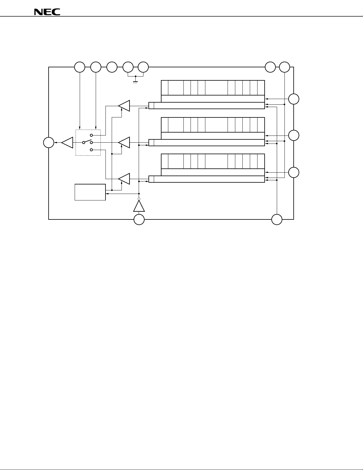
The µPD3794 is a color CCD (Charge Coupled Device) linear image sensor which changes optical images to
electrical signal and has the function of color separation.
µ
PD3794 has 3 rows of 2700 pixels, and each row has a single-sided readout type of charge transfer register.
The
And it has reset feed-through level clamp circuits, a clamp pulse generation circuit, an RGB selector and voltage
amplifiers. Therefore, it is suitable for 300 dpi/A4 color image scanners, color facsimiles and so on.
FEATURES
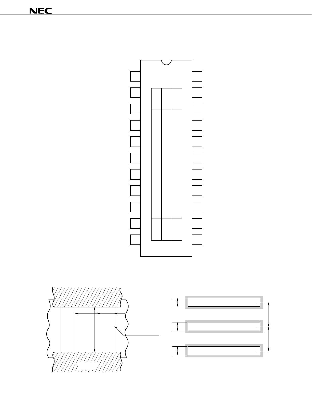
• Valid photocell : 2700 pixels × 3
• Photocell's pitch : 8 µm
• Line spacing : 32 µm (4 lines) Green line-Blue line, Blue line-Red line
7
• Color filter : Primary colors (red, green and blue), pigment filter (with light resistance 10
• Resolution : 12 dot/mm A4 (210 × 297 mm) size (shorter side)
300 dpi US letter (8.5” × 11”) size (shorter side)
• Drive clock level : CMOS output under 5 V operation
• Data rate : 4 MHz MAX.
• Power supply : +12 V
• On-chip circuits : Reset feed-through level clamp circuits
Clamp pulse generation circuit
RGB selector
Voltage amplifiers
lx•hour)
ORDERING INFORMATION
Part Number Package
µ
PD3794CY CCD linear image sensor 22-pin plastic DIP (400 mil)
Document No.S13125EJ1V0DS00(1st edition)
Date published December 1997 N CP(K)
Printed in Japan
The information in this document is subject to change without notice.
©
1997
BLOCK DIAGRAM
µ
PD3794
SEL1
SEL2 GND GNDV
22120
V
OUT
Clamp pulse
generator
OD
19 2 11 15 14
······
D15
······
D15
······
D15
3
φ
RB
D64
CCD analog shift register
D64
CCD analog shift register
D64
CCD analog shift register
Photocell
S1
S2
(Green)
Transfer gate
Photocell
S1
S2
(Blue)
Transfer gate
Photocell
S1
S2
(Red)
Transfer gate
S2699
S2700
S2699
S2700
S2699
S2700
D65
D65
D65
D66
D66
D66
D67
D67
D67
φ
GND 1
9
φ
2
13
12
10
φ
TG1
(Green)
φ
TG2
(Blue)
φ
TG3
(Red)
2
PIN CONFIGURATION (Top View)
Green photocell array
8 m
µ
Blue photocell array
8 m
µ
Red photocell array
8 m
µ
4 lines
(32 m)
µ
4 lines
(32 m)
µ
CCD linear image sensor 22-pin plastic DIP (400 mil)
µ
PD3794
Output signal
Ground
Reset gate clock
No connection
No connection
No connection
No connection
No connection
Shift register clock 2
Transfer gate clock 3
(for Red)
Ground
V
GND
φ
φ
TG3
GND
OUT
RB
NC
NC
NC
NC
NC
φ
1
2
1
1
1
3
4
5
6
Red
Blue
Green
7
8
9
2
10
2700
2700
2700
11
22NCSEL1
21
NC
SEL2
20
V
19
18
17
NC
16
NC
GND
15
14
φ
φ
13
12
φ
RGB select input 1
No connection
RGB select input2
Output drain voltage
OD
No connection
No connection
No connection
Ground
1
Shift register clock 1
Transfer gate clock 1
TG1
(for Green)
Transfer gate clock 2
TG2
(for Blue)
PHOTOCELL STRUCTURE DIAGRAM PHOTOCELL ARRAY STRUCTURE DIAGRAM
(Line spacing)
3
m
µ
Channel stopper
5 m
µ
Aluminum
shield
µ
8 m
3
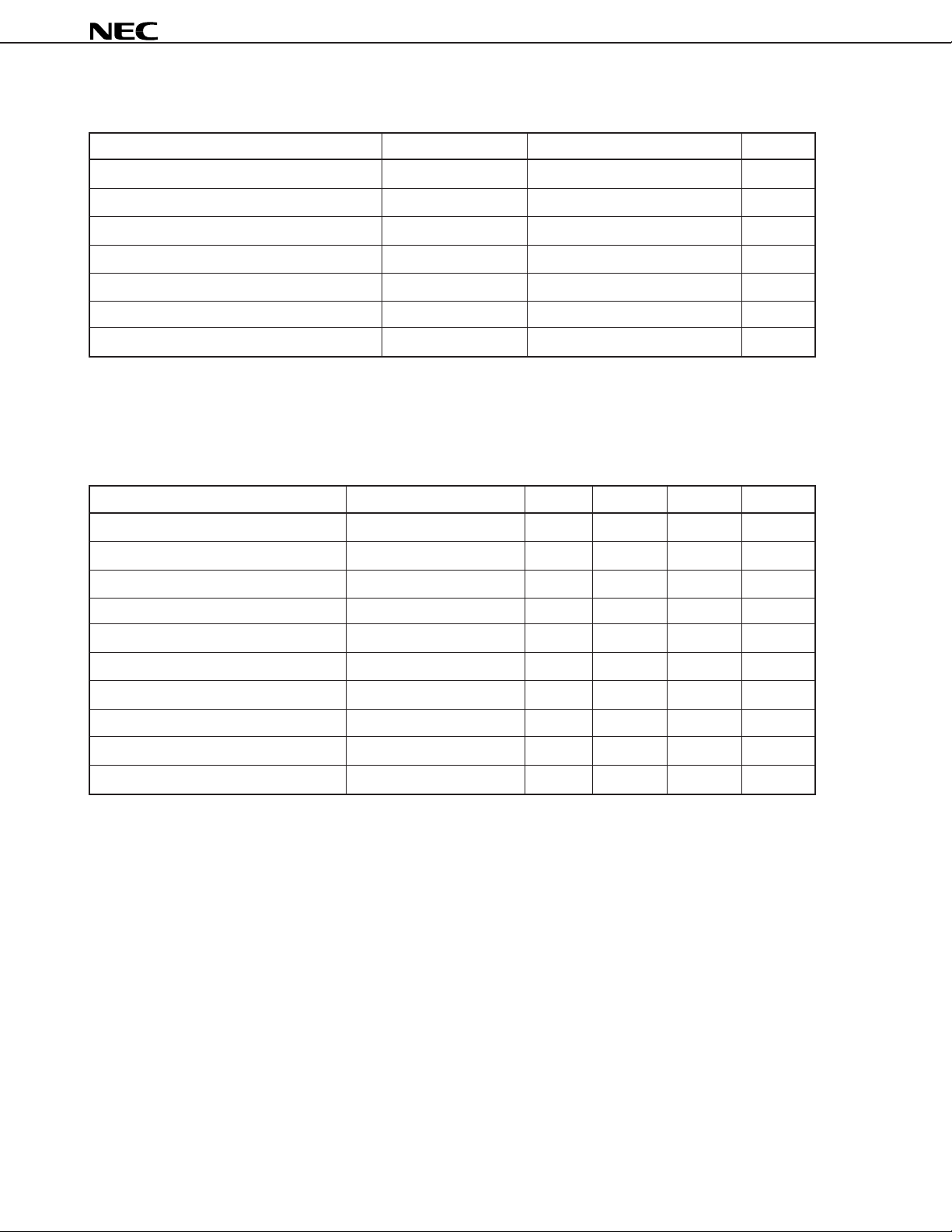
ABSOLUTE MAXIMUM RATINGS (TA = +25 °C)
Parameter Symbol Ratings Unit
Output drain voltage VOD –0.3 to +15 V
µ
PD3794
Shift register clock voltage V
Reset gate clock voltage V
Transfer gate clock voltage V
φ
1, Vφ2 –0.3 to +8 V
φ
RB –0.3 to +8 V
φ
TG1
to V
φ
TG3 –0.3 to +8 V
RGB select input voltage VSEL1,VSEL2 –0.3 to +8 V
Operating ambient temperature TA –25 to +60 °C
Storage temperature Tstg –40 to +70 °C
Caution Exposure to ABSOLUTE MAXIMUM RATINGS for extended periods may affect device reliability;
exceeding the ratings could cause permanent damage. The parameters apply independently.
RECOMMENDED OPERATING CONDITIONS (TA = +25 °C)
Parameter Symbol MIN. TYP. MAX. Unit
Output drain voltage VOD 11.4 12.0 12.6 V
Shift register clock high level V
Shift register clock low level V
Reset gate clock high level V
Reset gate clock low level V
Transfer gate clock high level V
Transfer gate clock low level V
RGB select input high level VSEL1H, VSEL2H 4.5 5.0 5.5 V
φ
1H, Vφ2H 4.5 5.0 5.5 V
φ
1L, Vφ2L –0.3 0 +0.5 V
φ
RBH 4.5 5.0 5.5 V
φ
RBL –0.3 0 +0.5 V
φ
TG1H
φ
TG1L
to V
φ
TG3H 4.5 V
to V
φ
TG3L –0.3 0 +0.5 V
Note
φ
1H
Note
V
φ
1H
V
RGB select input low level VSEL1L, VSEL2L –0.3 0 +0.5 V
Data rate f
Note When Transfer gate clock high level (V
φ
RB – 1.0 4.0 MHz
φ
TG1H to VφTG3H) is higher than Shift register clock high level (Vφ1H),
Image lag can increase.
4
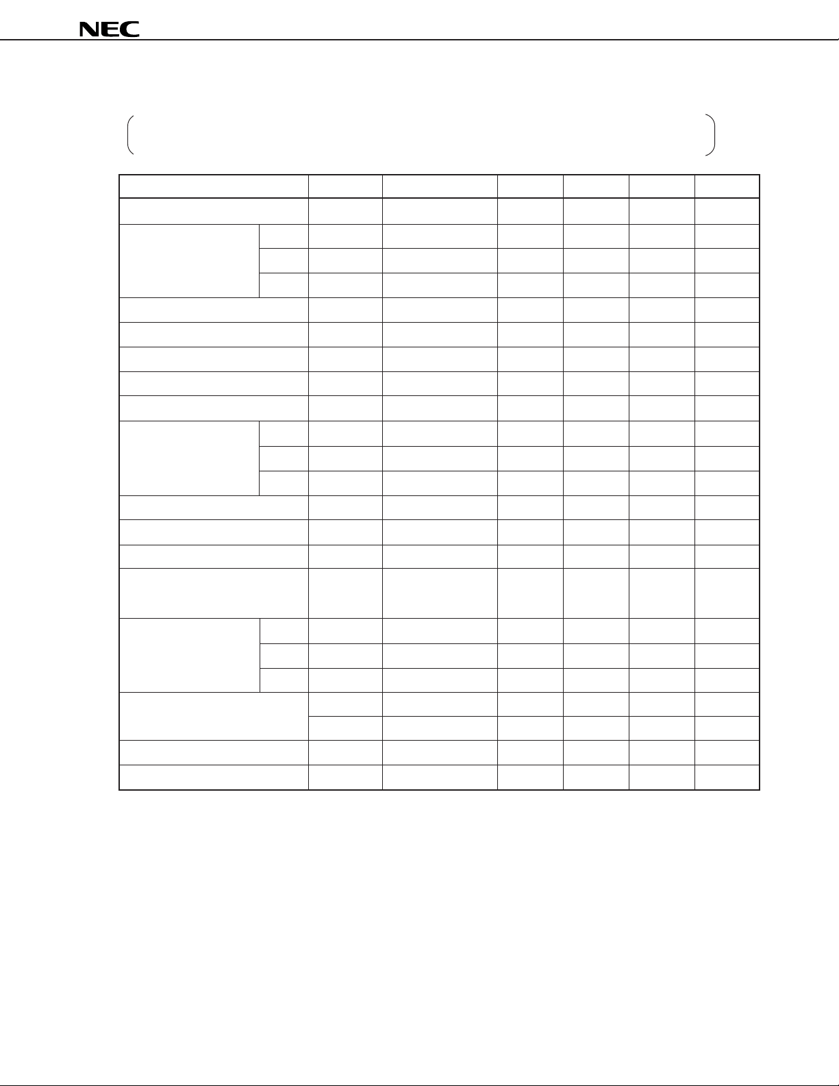
ELECTRICAL CHARACTERISTICS
µ
PD3794
TA = +25 °C, VOD = 12 V, data rate (f
φ
RB) = 1 MHz, storage time = 10 ms,
light source: 3200 K halogen lamp +C-500S (infrared cut filter, t = 1mm), input signal clock = 5 Vp-p
Parameter Symbol Test Conditions MIN. TYP. MAX. Unit
Saturation voltage Vsat 2.0 3.0 V
Saturation exposure Red SER 0.205 lx•s
Green SEG 0.225 lx•s
Blue SEB 0.375 lx•s
Photo response non-uniformity PRNU VOUT = 1.0 V 6 20 %
Average dark signal ADS Light shielding 0.5 5.0 mV
Dark signal non-uniformity DSNU Light shielding 4.0 10.0 mV
Power consumption PW 300 600 mW
Output impedance ZO 0.5 1 kΩ
Response Red RR 10.3 14.6 18.9 V/lx•s
Green RG 9.4 13.3 17.2 V/lx•s
Blue RB 5.6 8.0 10.4 V/lx•s
Image lag IL VOUT = 1.0 V 5.0 10.0 %
Offset level
Output fall delay time
Note1
Note2
VOS 4.5 6.0 7.5 V
td VOUT = 1.0 V 70 ns
Total transfer efficiency TTE VOUT = 1.0 V, 92 98 %
data rate = 4 MHz
Response peak Red 630 nm
Green 540 nm
Blue 460 nm
Dynamic range DR1 Vsat /DSNU 750 times
DR2 Vsat /σ 3000 times
Reset feed-through noise
Random noise σ Light shielding – 1.0 – mV
Note1
RFTN Light shielding –1000 –300 +500 mV
Notes 1. Refer to TIMING CHART 2.
2. When the fall time of
φ
1 (t1) is the TYP. value (refer to TIMING CHART 2).
5
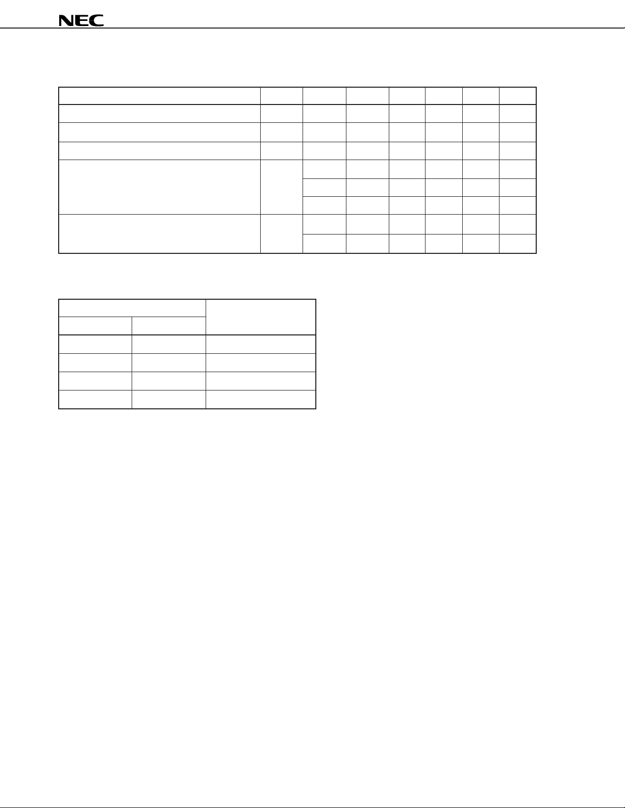
INPUT PIN CAPACITANCE (TA = +25 °C, VOD = 12 V)
Parameter Symbol Pin name Pin No. MIN. TYP. MAX. Unit
µ
PD3794
Shift register clock pin capacitance 1 C
Shift register clock pin capacitance 2 C
Reset gate clock pin capacitance C
Transfer gate clock pin capacitance C
φ
1
φ
2
φ
RB
φ
TG
φ
1 14 300 pF
φ
2 9 300 pF
φ
RB 3 20 pF
φ
TG1 13 50 pF
φ
TG2 12 50 pF
φ
TG3 10 50 pF
RGB select input pin capacitance CSEL SEL1 22 50 pF
SEL2 20 50 pF
RGB SELECT FUNCTION
RGB select input
SEL1 SEL2
High level High level Blue
High level Low level Green
Low level High level Red
Low level Low level Prohibited
Output color
6
 Loading...