NEC UPD3788D Datasheet

DATA SHEET
MOS INTEGRATED CIRCUIT
µ
PD3788
7300 PIXELS × 3 COLOR CCD LINEAR IMAGE SENSOR
The µPD3788 is a high-speed and high sensitive color CCD (Charge Coupled Device) linear image sensor which
changes optical images to electrical signal and has the function of color separation.
µ
PD3788 has 3 rows of 7300 pixels, and it is a 2-output/color type CCD sensor with 2 rows/color of charge
The
transfer register, which transfers the photo signal electrons of 7300 pixels separately in odd and even pixels.
Moreover, the spectral response characteristics of the µPD3788 is modified from the previous device µPD3728 to be
suitable for Xe-lamp. Therefore, it is suitable for 600 dpi/A3 high-speed color digital copiers and so on.
FEATURES
• Valid photocell : 7300 pixels × 3
• Photocell pitch : 10 µm
2
µ
• Photocell size : 10 × 10
• Line spacing : 40 µm (4 lines) Red line-Green line, Green line-Blue line
• Color filter : Primary colors (red, green and blue), pigment filter (with light resistance 107 lx•hour)
• Resolution : 24 dot/mm (600 dpi) A3 (297 × 420 mm) size (shorter side)
• Drive clock level : CMOS output under 5 V operation
• Data rate : 40 MHz MAX. (20 MHz/1 output)
• Output type : 2 outputs in phase/color
• Power supply : +12 V
• On-chip circuits : Reset feed-through level clamp circuits
Voltage amplifiers
ORDERING INFORMATION
Part Number Package
µ
PD3788D CCD linear image sensor 36-pin ceramic DIP (15.24 mm (600))
m
The information in this document is subject to change without notice. Before using this document, please
confirm that this is the latest version.
Not all devices/types available in every country. Please check with local NEC representative for availability
and additional information.
Document No. S14664EJ1V0DS00(1st edition)
Date published June 2000 N CP(K)
Printed in Japan
©
2000
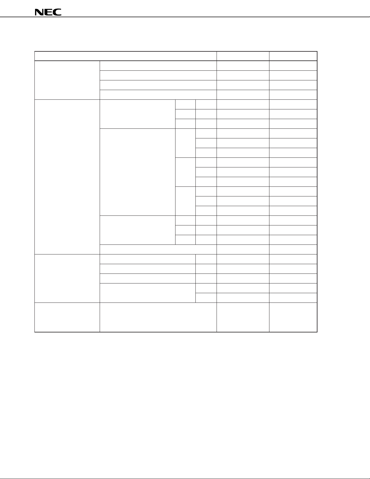
COMPARISON CHART
µ
PD3788
Item
ABSOLUTE MAXIMUM Shift register clock voltage (V) –0.3 to +8 –0.3 to +15
RATINGS Reset gate clock voltage (V) –0.3 to +8 –0.3 to +15
Reset feed-through level clamp clock voltage (V) –0.3 to +8 –0.3 to +15
Transfer gate clock voltage (V) –0.3 to +8 –0.3 to +15
ELECTRICAL Saturation exposure (Ix·s) Red TYP. 0.36 0.35
CHARACTERISTICS Green TYP. 0.37 0.39
Blue TYP. 0.80 0.31
Response (V/Ix·s) Red MIN. 3.85 3.9
TYP. 5.5 5.6
MAX. 7.15 7.3
Green MIN. 3.78 3.6
TYP. 5.4 5.1
MAX. 7.02 6.6
Blue MIN. 1.75 4.5
TYP. 2.5 6.4
MAX. 3.25 8.3
Response peak (nm) Red TYP. 645 630
Green TYP. 540 540
Blue TYP. 445 460
Random noise test conditions tcp = 20 ns t7 = 150 ns
TIMING CHART t3 (ns) MIN. 17 20
t7 (ns) MIN. 17 20
t10 (ns) MIN. –20 –10
tCP (ns) MIN. 5 –
TYP. 150 –
STANDARD TOTAL SPECTRAL modified –
CHARACTERISTIC RESPONSE CHARACTERISTICS
CURVES
µ
PD3788
µ
PD3728
2
Data Sheet S14664EJ1V0DS00
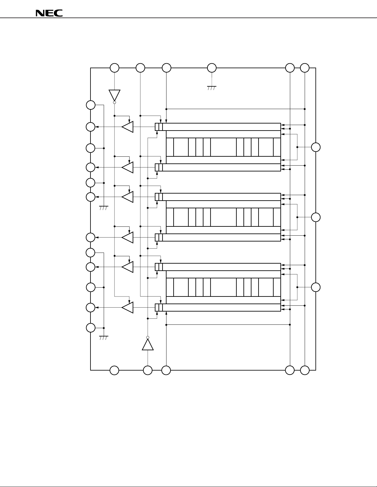
BLOCK DIAGRAM
20
φ
CLB 1L GND
30
φφφ
29
φ
28
16
23
µ
PD3788
21
24
GND
V
OUT
2
(Blue, even)
GND
V
OUT
1
(Blue, odd)
GND
OUT
3
V
(Green, odd)
V
OUT
4
(Green, even)
GND
OUT
6
V
(Red, even)
GND
V
OUT
5
(Red, odd)
31
32
CCD analog shift register
Transfer gate
33
. . . . . . . . . .
D27
D128
S1
Photocell
S2
(Blue)
Transfer gate
34
CCD analog shift register
35
36
CCD analog shift register
Transfer gate
. . . . . . . . . .
D27
D128
S1
Photocell
S2
(Green)
Transfer gate
1
CCD analog shift register
2
3
CCD analog shift register
Transfer gate
4
. . . . . . . . . .
D27
D128
S1
Photocell
S2
(Red)
Transfer gate
5
CCD analog shift register
S7300
S7299
S7300
S7299
S7300
S7299
D129
D129
D129
D134
D134
D134
TG1
φ
22
(Blue)
TG2
φ
21
(Green)
φ
TG3
15
(Red)
GND
6
8
7
OD
V
RB
9
φ
10
Data Sheet S14664EJ1V0DS00
13 14
φφφ
12
3
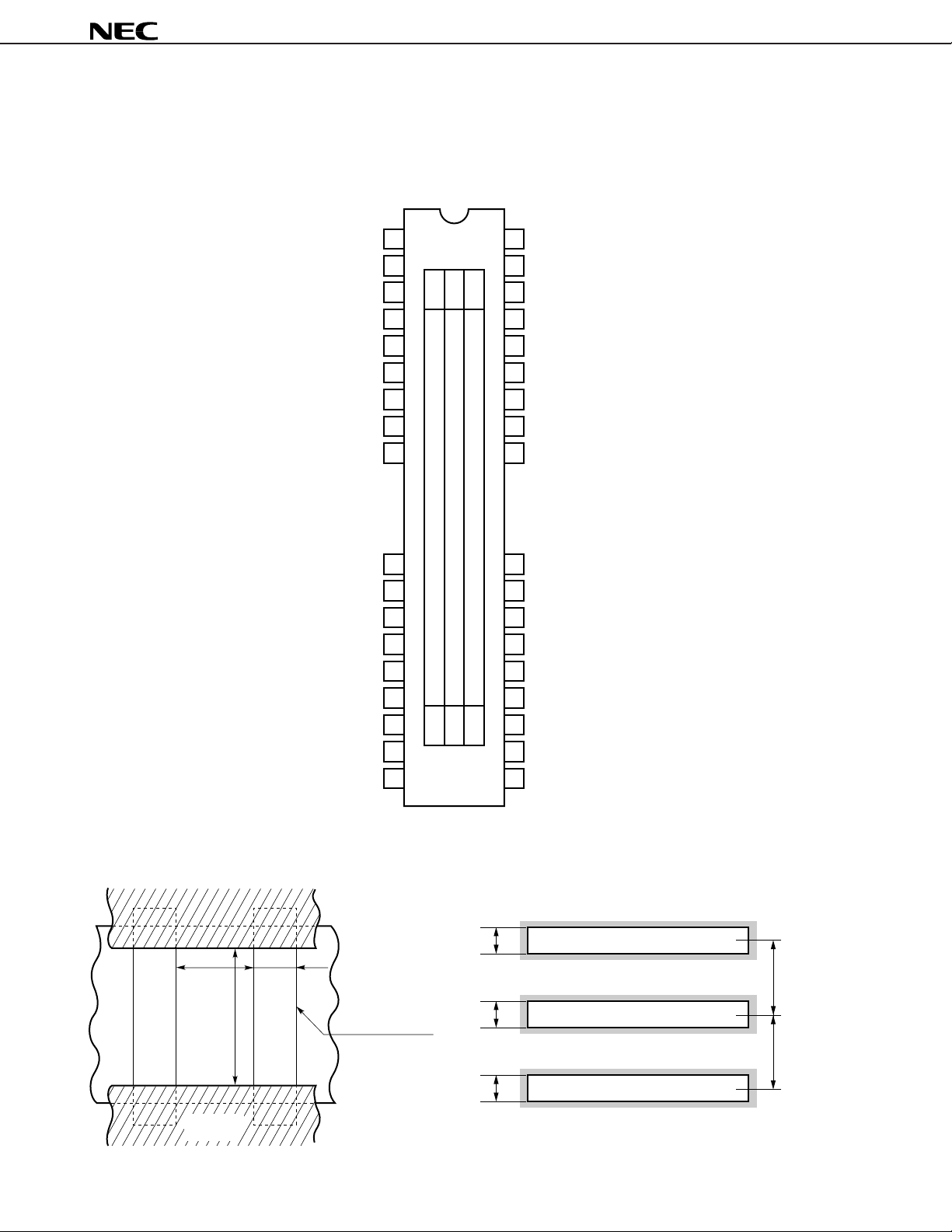
PIN CONFIGURATION (Top View)
CCD linear image sensor 36-pin ceramic DIP (15.24 mm (600))
•µPD3788D
V
1
OUT
Output signal 4 (Green, even)
4
36
V
Output signal 3 (Green, odd)
OUT
3
µ
PD3788
Ground
Output signal 6 (Red, even)
Ground
Output signal 5 (Red, odd)
Ground
Output drain voltage
Reset gate clock
Shift register clock 10
No connection
No connection
No connection
Shift register clock 1
Shift register clock 2
Transfer gate clock 3 (for Red)
GND
V
GND
V
GND
φ
φ
OUT
OUT
V
OD
RB
φ
10
NC
NC
NC
φ
φ
TG3
2
1
1
Red
1
Blue
Green
3
6
4
5
5
6
7
8
9
10
11
12
1
13
2
14
15
35
34
33
32
31
30
29
28
27
26
25
24
23
22
GND
V
OUT
GND
V
OUT
GND
φ
CLB
φ
1L
φ
20
NC
NC
NC
2
φ
1
φ
φ
TG1
Output signal 1 (Blue, odd)
1
Ground
Output signal 2 (Blue, even)
2
Ground
Reset feed-through level
clamp clock
Last stage shift register clock 1
Shift register clock 20
No connection
No connection
No connection
Shift register clock 2
Shift register clock 1
Transfer gate clock 1 (for Blue)
Ground
Ground
No connection
No connection
GND
NC
NC
16
17
18
7300
7300
7300
21
20
19
φ
Transfer gate clock 2 (for Green)
TG2
No connection
NC
No connection
NC
PHOTOCELL STRUCTURE DIAGRAM PHOTOCELL ARRAY STRUCTURE DIAGRAM
(Line spacing)
10 m
7 m
µ
Aluminum
shield
µ
10 m
3
m
µ
Channel stopper
µ
10 m
µ
10 m
µ
Blue photocell array
(40 m)
Green photocell array
(40 m)
Red photocell array
4 lines
µ
4 lines
µ
4
Data Sheet S14664EJ1V0DS00
µ
PD3788
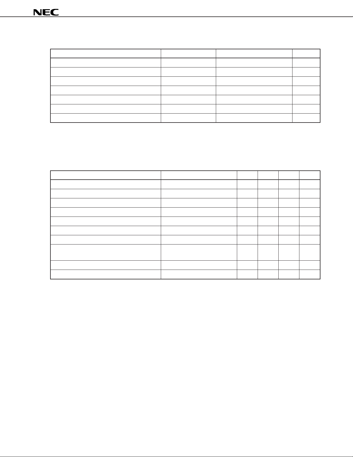
ABSOLUTE MAXIMUM RATINGS (TA = +25 °C)
Parameter Symbol Ratings Unit
Output drain voltage VOD –0.3 to +15 V
Shift register clock voltage V
Reset gate clock voltage V
Reset feed-through level clamp clock voltage V
Transfer gate clock voltage V
φ
1, Vφ1L, Vφ10, Vφ2, Vφ20 –0.3 to +8 V
φ
RB –0.3 to +8 V
φ
CLB –0.3 to +8 V
φ
TG1
to V
φ
TG3 –0.3 to +8 V
Operating ambient temperature TA –25 to +60 °C
Storage temperature Tstg –40 to +100 °C
Caution Exposure to ABSOLUTE MAXIMUM RATINGS for extended periods may affect device reliability;
exceeding the ratings could cause permanent damage. The parameters apply independently.
RECOMMENDED OPERATING CONDITIONS (TA = +25 °C)
Parameter Symbol MIN. TYP. MAX. Unit
Output drain voltage VOD 11.4 12.0 12.6 V
Shift register clock high level V
Shift register clock low level V
Reset gate clock high level V
Reset gate clock low level V
Reset feed-through level clamp clock high level V
Reset feed-through level clamp clock low level V
Transfer gate clock high level
Note
Transfer gate clock low level V
Data rate 2f
φ
1H, Vφ1LH, Vφ10H, Vφ2H, Vφ20H 4.5 5.0 5.5 V
φ
1L, Vφ1LL, Vφ10L, Vφ2L, Vφ20L –0.3 0 +0.5 V
φ
RBH 4.5 5.0 5.5 V
φ
RBL –0.3 0 +0.5 V
φ
CLBH 4.5 5.0 5.5 V
φ
CLBL –0.3 0 +0.5 V
V
φ
TG1H
to V
φ
TG3H 4.5 Vφ1H Vφ1H V
φ
TG1L
to V
φ
TG3L –0.3 0 +0.5 V
φ
RB – 2 40 MHz
(V
φ
10H)(Vφ10H)
Note When Transfer gate clock high level (V
Image lag can increase.
φ
Remark Pin 9 (
10) and pin 28 (φ20) should be open to decrease the influence of input clock noise to output signal
waveform, in case of operating at low or middle speed range; data rate under 24 MHz or so.
φ
TG1H to VφTG3H) is higher than Shift register clock high level (Vφ1H (Vφ10H)),
Data Sheet S14664EJ1V0DS00
5
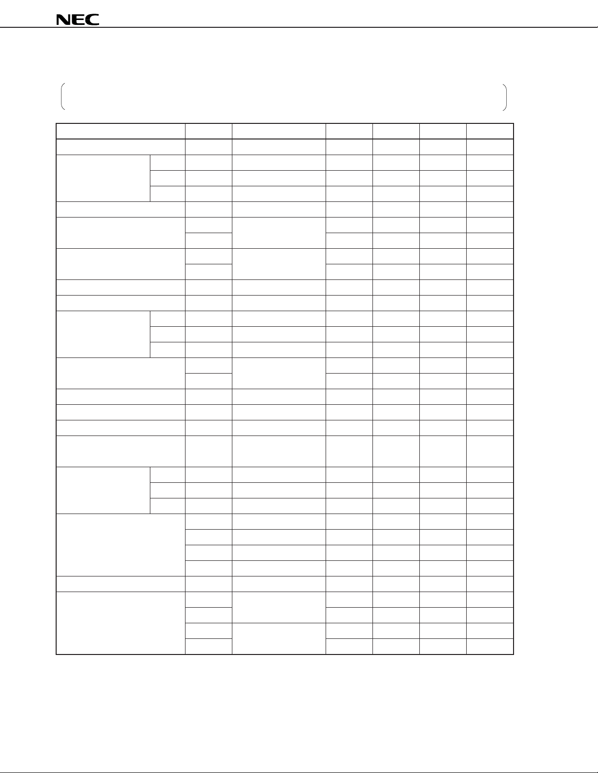
ELECTRICAL CHARACTERISTICS
µ
PD3788
TA = +25 °C, VOD = 12 V, f
φ
RB = 1 MHz, data rate = 2 MHz, storage time = 10 ms, input signal clock = 5 Vp-p,
light source: 3200 K halogen lamp +C-500S (infrared cut filter, t = 1mm) +HA-50 (heat absorbing filter, t = 3mm)
Parameter Symbol Test Conditions MIN. TYP. MAX. Unit
Saturation voltage Vsat 1.5 2.0 – V
Saturation exposure Red SER 0.36 lx•s
Green SEG 0.37 lx•s
Blue SEB 0.80 lx•s
Photo response non-uniformity PRNU VOUT = 1 V 6 18 %
Note 1
Note 1
Note 1
Note 1
Green RG 3.78 5.4 7.02 V/lx•s
Blue RB 1.75 2.5 3.25 V/lx•s
Note 3
Green 540 nm
Blue 445 nm
Note 2
ADS1 Light shielding 1.0 5.0 mV
ADS2 0.5 5.0 mV
DSNU1 Light shielding 2.0 5.0 mV
DSNU2 1.0 5.0 mV
IL1 VOUT = 1 V 2.0 5.0 %
IL2 1.0 5.0 %
VOS 4.0 5.0 6.0 V
td VOUT = 1 V 20 ns
data rate = 40 MHz
DR11 Vsat/DSNU1 1000 times
DR12 Vsat/DSNU2 2000 times
DR21 Vsat/σbit1 2000 times
DR22 Vsat/σbit2 4000 times
RFTN Light shielding –500 +200 +500 mV
σbit1 Light shielding, bit clamp – 1 .0 – mV
σbit2 mode (tcp = 20 ns) – 0.5 – mV
σline1 Light shielding, line – 4.0 – mV
σline2 clamp mode (t19 = 3 µs) – 2.0 – mV
Average dark signal
Dark signal non-uniformity
Power consumption P W 600 800 mW
Output impedance ZO 0.3 0.5 kΩ
Response Red RR 3.85 5.5 7.15 V/lx•s
Image lag
Offset level
Output fall delay time
Register imbalance RI VOUT = 1 V 0 4.0 %
Total transfer efficiency TTE VOUT = 1 V, 95 98 %
Response peak Red 645 nm
Dynamic range
Reset feed-through noise
Random noise
Note 1
Note 2
Notes 1. ADS1, DSNU1, IL1, DR11, DR21, σbit1 and σline1 show the specification of VOUT1 and VOUT2.
ADS2, DSNU2, IL2, DR12, DR22, σbit2 and σline2 show the specification of VOUT3 to VOUT6.
2. Refer to TIMING CHART 2, 5.
φ
3. When the fall time of
6
1L (t2’) is the TYP. value (refer to TIMING CHART 2, 5).
Data Sheet S14664EJ1V0DS00

INPUT PIN CAPACITANCE (TA = +25 °C, VOD = 12 V)
Parameter Symbol Pin name Pin No. MIN. TYP. MAX. Unit
Shift register clock pin capacitance 1 C
Shift register clock pin capacitance 2 C
Last stage shift register clock pin capacitance C
Reset gate clock pin capacitance C
Reset feed-through level clamp clock pin capacitance C
Transfer gate clock pin capacitance C
φ
1
φ
2
φ
L
φ
RB
φ
CLB
φ
TG
µ
PD3788
φ
1 13 350 500 pF
23 350 500 pF
φ
10 9 350 500 pF
φ
2 14 350 500 pF
24 350 500 pF
φ
20 28 350 500 pF
φ
1L 29 10 pF
φ
RB 8 10 pF
φ
CLB 30 10 pF
φ
TG1 22 100 pF
φ
TG2 21 100 pF
φ
TG3 15 100 pF
Remark Pins 13, 23 (φ1) and pin 9 (φ10) are connected each other inside of the device.
Pins 14, 24 (φ2) and pin 28 (φ20) are connected each other inside of the device.
Data Sheet S14664EJ1V0DS00
7
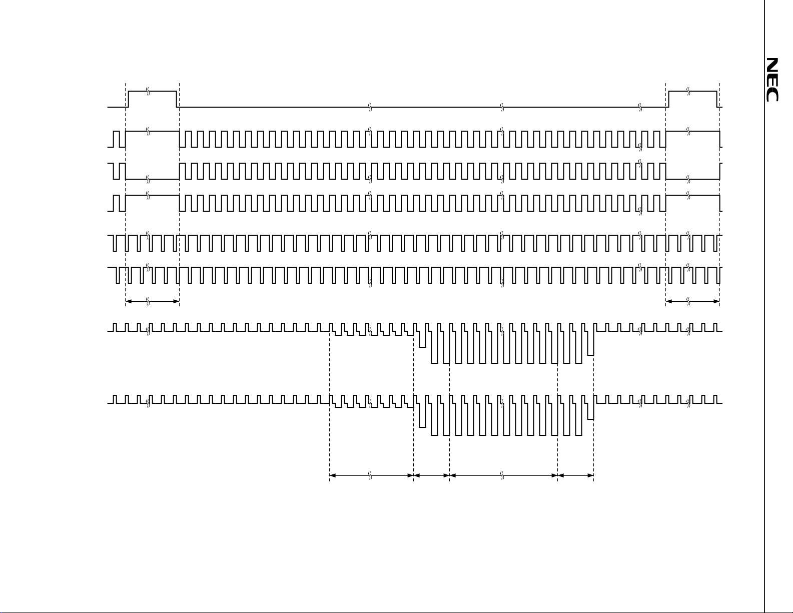
8
TIMING CHART 1 (Bit clamp mode, for each color)
φ
TG1 to
φ
TG3
1 ( 10)
φ
φ
2 ( 20)
φ
φ
φ
1L
Data Sheet S14664EJ1V0DS00
φ
RB
φ
CLB
V
OUT
1, 3, 5
V
OUT
2, 4, 6
Note Input the
Note Note
91113
7
101214
8
1517192123
1618202224
25
26
27
28
29
30
Optical black
(96 pixels)
119
121
123
125
120
122
124
126
Invalid photocell
(6 pixels)
127
128
129
131132
130
Valid photocell
(7300 pixels)
7425
7427
7429
7431
7426
7428
7430
7432
Invalid photocell
(6 pixels)
7433
7434
7435
7436
7437
7438
φ
RB and
135
246
φ
CLB pulses continuously during this period, too.
µ
PD3788
 Loading...