NEC UPD3729D Datasheet

DATA SHEET
MOS INTEGRATED CIRCUIT
µ
PD3729
5000 PIXELS × 3 COLOR CCD LINEAR IMAGE SENSOR
The µPD3729 is a high-speed and high sensitive color CCD (Charge Coupled Device) linear image sensor which
changes optical images to electrical signal and has the function of color separation.
µ
PD3729 has 3 rows of 5000 pixels, and it is a 2-output/color type CCD sensor with 2 rows/color of charge
The
transfer register, which transfers the photo signal electrons of 5000 pixels separately in odd and even pixels.
Therefore, it is suitable for 400 dpi/A3 high-speed color digital copiers and so on.
FEATURES
• Valid photocell : 5000 pixels × 3
• Photocell's pitch : 10 µm
• Line spacing : 40 µm (4 lines) Red line-Green line, Green line-Blue line
7
• Color filter : Primary colors (red, green and blue), pigment filter (with light resistance 10
• Resolution : 16 dot/mm (400 dpi) A3 (297 × 420 mm) size (shorter side)
• Drive clock level : CMOS output under 5 V operation
• Data rate : 30 MHz MAX. (15 MHz/1 output)
• Output type : 2 outputs in phase/color
• Power supply : +12 V
• On-chip circuits : Reset feed-through level clamp circuits
Voltage amplifiers
lx•hour)
ORDERING INFORMATION
Part Number Package
µ
PD3729D CCD linear image sensor 24-pin ceramic DIP (400 mil)
Document No. S12883EJ1V0DS00(1st edition)
Date published November 1998 N CP(K)
Printed in Japan
The information in this document is subject to change without notice.
©
1998
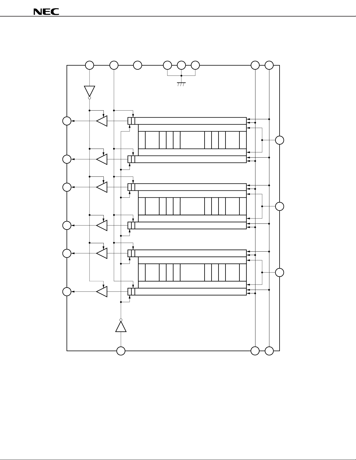
BLOCK DIAGRAM
µ
PD3729
V
OUT
2
(Blue, even)
OUT
1
V
(Blue, odd)
V
OUT
3
(Green, odd)
V
OUT
4
(Green, even)
22
23
24
1
φ
CLB 1L GND GNDV
20
φφφ
19
OD
12
5
4
21
CCD analog shift register
Transfer gate
. . . . . . . . . .
D27
D128
S1
Photocell
S2
(Blue)
S5000
S4999
D129
Transfer gate
CCD analog shift register
CCD analog shift register
Transfer gate
. . . . . . . . . .
D27
D128
S1
Photocell
S2
(Green)
S5000
S4999
D129
Transfer gate
CCD analog shift register
D134
D134
15
16
21GND
φ
TG1
14
(Blue)
TG2
φ
13
(Green)
V
OUT
6
(Red, even)
V
OUT
5
(Red, odd)
2
3
6
RB
CCD analog shift register
Transfer gate
. . . . . . . . . .
D27
D128
S1
Photocell
S2
(Red)
S5000
S4999
D129
Transfer gate
CCD analog shift register
D134
910
12
φ
TG3
11
(Red)
φφφ
2
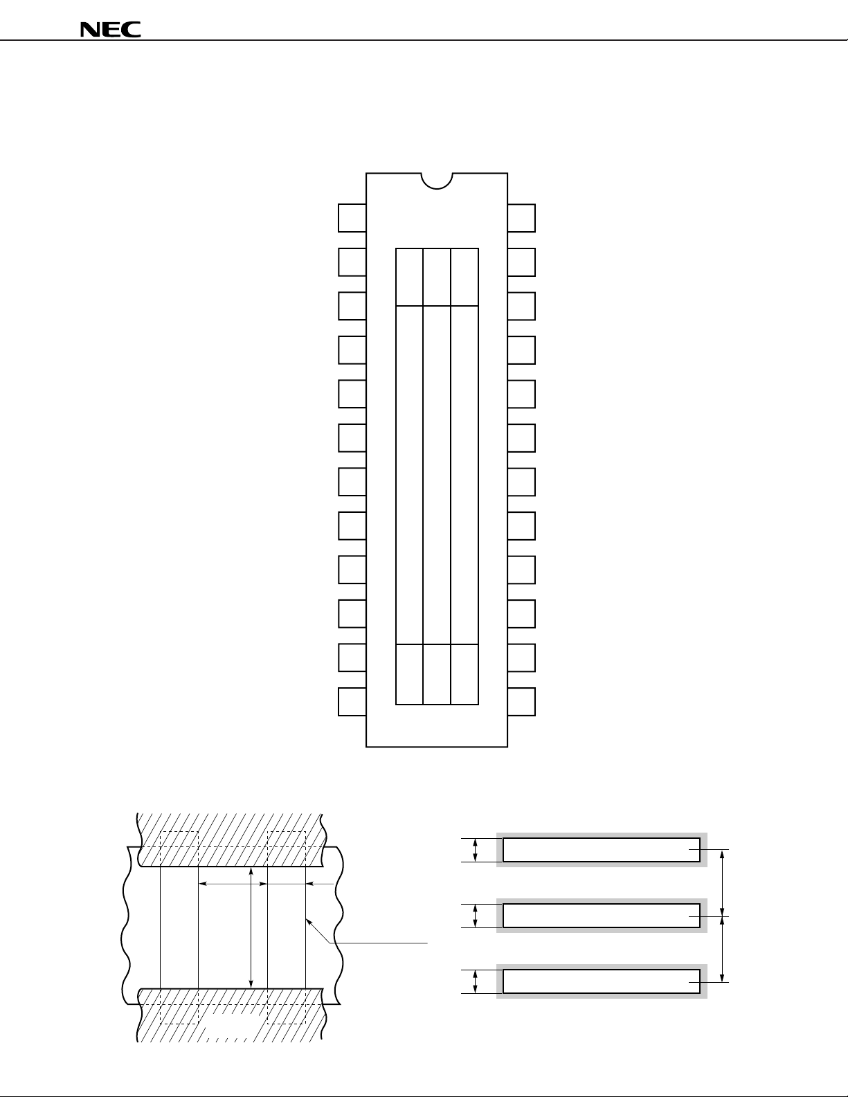
PIN CONFIGURATION (Top View)
Blue photocell array
10 m
µ
Green photocell array
10 m
µ
Red photocell array
10 m
µ
4 lines
(40 m)
µ
4 lines
(40 m)
µ
CCD linear image sensor 24-pin ceramic DIP (400 mil)
•µPD3729D
1V
OUT
4Output signal 4 (Green, even)
24
OUT
3
Output signal 3 (Green, odd)
V
µ
PD3729
Ground
Output drain voltage
Reset gate clock
No connection
No connection
Shift register clock 1
Shift register clock 2
Transfer gate clock 3 (for Red)
OUT
OUT
2V
6Output signal 6 (Red, even)
1
1
1
5Output signal 5 (Red, odd)
3V
4GND
OD
5V
6RB
7NC
8NC
φ
91
102
φ
11TG3
Red
Green
Blue
23
22
21
20
19
18
17
16
15
14
OUT
1 Output signal 1 (Blue, odd)
V
V
OUT
2
Output signal 2 (Blue, even)
GND
Ground
Reset feed-through level
φ
CLB
clamp clock
φφ
1L
Last stage shift register clock 1
NC
No connection
NC
No connection
φ
2
Shift register clock 2
φ
1
Shift register clock 1
φφ
TG1
Transfer gate clock 1 (for Blue)
5000
5000
5000
Ground
12GND
13
φ
TG2
Transfer gate clock 2 (for Green)
PHOTOCELL STRUCTURE DIAGRAM PHOTOCELL ARRAY STRUCTURE DIAGRAM
(Line spacing)
3
m
µ
Channel stopper
Aluminum
shield
7 m
µ
µ
10 m
3
µ
PD3729
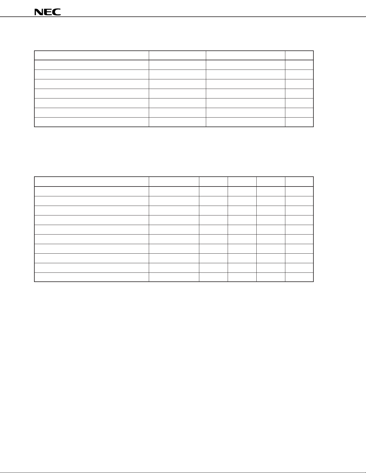
ABSOLUTE MAXIMUM RATINGS (TA = +25 °C)
Parameter Symbol Ratings Unit
Output drain voltage VOD –0.3 to +15 V
Shift register clock voltage V
Reset gate clock voltage V
Reset feed-through level clamp clock voltage V
Transfer gate clock voltage V
φ
1, Vφ1L, Vφ2 –0.3 to +15 V
φ
RB –0.3 to +15 V
φ
CLB –0.3 to +15 V
φ
TG1
to V
φ
TG3 –0.3 to +15 V
Operating ambient temperature TA –25 to +70 °C
Storage temperature Tstg –40 to +100 °C
Caution Exposure to ABSOLUTE MAXIMUM RATINGS for extended periods may affect device reliability;
exceeding the ratings could cause permanent damage. The parameters apply independently.
RECOMMENDED OPERATING CONDITIONS (TA = +25 °C)
Parameter Symbol MIN. TYP. MAX. Unit
Output drain voltage VOD 11.4 12.0 12.6 V
Shift register clock high level V
Shift register clock low level V
Reset gate clock high level V
Reset gate clock low level V
Reset feed-through level clamp clock high level V
Reset feed-through level clamp clock low level V
Transfer gate clock high level V
Transfer gate clock low level V
Data rate 2f
φ
1H, Vφ1LH, Vφ2H 4.5 5.0 5.5 V
φ
1L, Vφ1LL, Vφ2L –0.3 0 +0.5 V
φ
RBH 4.5 5.0 5.5 V
φ
RBL –0.3 0 +0.5 V
φ
CLBH 4.5 5.0 5.5 V
φ
CLBL –0.3 0 +0.5 V
φ
TG1H
to V
φ
TG3H 4.5 V
φ
TG1L
to V
φ
TG3L –0.3 0 +0.5 V
φ
RB – 2 30 MHz
Note
φ
1H
Note
V
φ
1H
V
Note When Transfer gate clock high level (V
lag can increase.
4
φ
TG1H to VφTG3H) is higher than Shift register clock high level (Vφ1H), Image
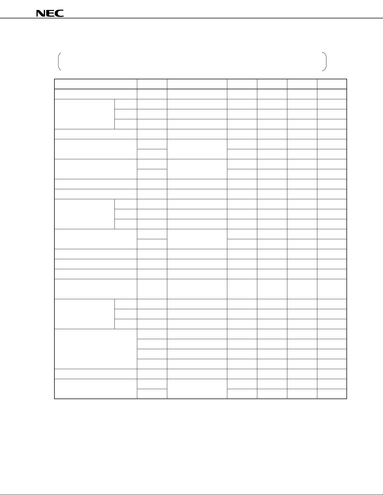
ELECTRICAL CHARACTERISTICS
µ
PD3729
TA = +25 °C, VOD = 12 V, f
φ
RB = 1 MHz, data rate = 2 MHz, storage time = 10 ms,
light source: 3200 K halogen lamp +C-500S (infrared cut filter, t = 1mm), input signal clock = 5 Vp-p
Parameter Symbol Test Conditions MIN. TYP. MAX. Unit
Saturation voltage Vsat 1.5 2.0 – V
Saturation exposure Red SER 0.32 lx•s
Green SEG 0.37 lx•s
Blue SEB 0.29 lx•s
Photo response non-uniformity PRNU VOUT = 1 V 6 18 %
Note 1
Note 1
Note 1
Note 1
Green RG 3.8 5.4 7.0 V/lx•s
Blue RB 4.7 6.8 8.9 V/lx•s
Note 3
Green 540 nm
Blue 460 nm
Note 2
ADS1 Light shielding 1.0 5.0 mV
ADS2 0.5 5.0 mV
DSNU1 Light shielding 2.0 5.0 mV
DSNU2 1.0 5.0 mV
IL1 VOUT = 1 V 2.0 5.0 %
IL2 1.0 5.0 %
VOS 4.0 5.0 6.0 V
td VOUT = 1 V 25 ns
data rate = 30 MHz
DR11 Vsat /DSNU1 1000 times
DR12 Vsat/DSNU2 2000 times
DR21 Vsat /σ1 2000 times
DR22 Vsat/σ2 4000 times
RFTN Light shielding –500 +200 +500 mV
σ1 Light shielding – 1.0 – mV
σ2 – 0.5 – mV
Average dark signal
Dark signal non-uniformity
Power consumption P W 500 700 mW
Output impedance ZO 0.3 0.5 kΩ
Response Red RR 4.3 6.2 8.1 V/lx•s
Image lag
Offset level
Output fall delay time
Register imbalance RI VOUT = 1 V 0 4.0 %
Total transfer efficiency TTE VOUT = 1 V, 95 98 %
Response peak Red 630 nm
Dynamic range
Reset feed-through noise
Random noise
Note 1
Note 2
Notes 1. ADS1, DSNU1, IL1, DR11 and DR21 show the specification of VOUT1 and VOUT2.
ADS2, DSNU2, IL2, DR12 and DR22 show the specification of V
OUT3 to VOUT6.
2. Refer to TIMING CHART 2.
3. When the fall time of φ1L (t2’) is the TYP. value (refer to TIMING CHART 2).
5
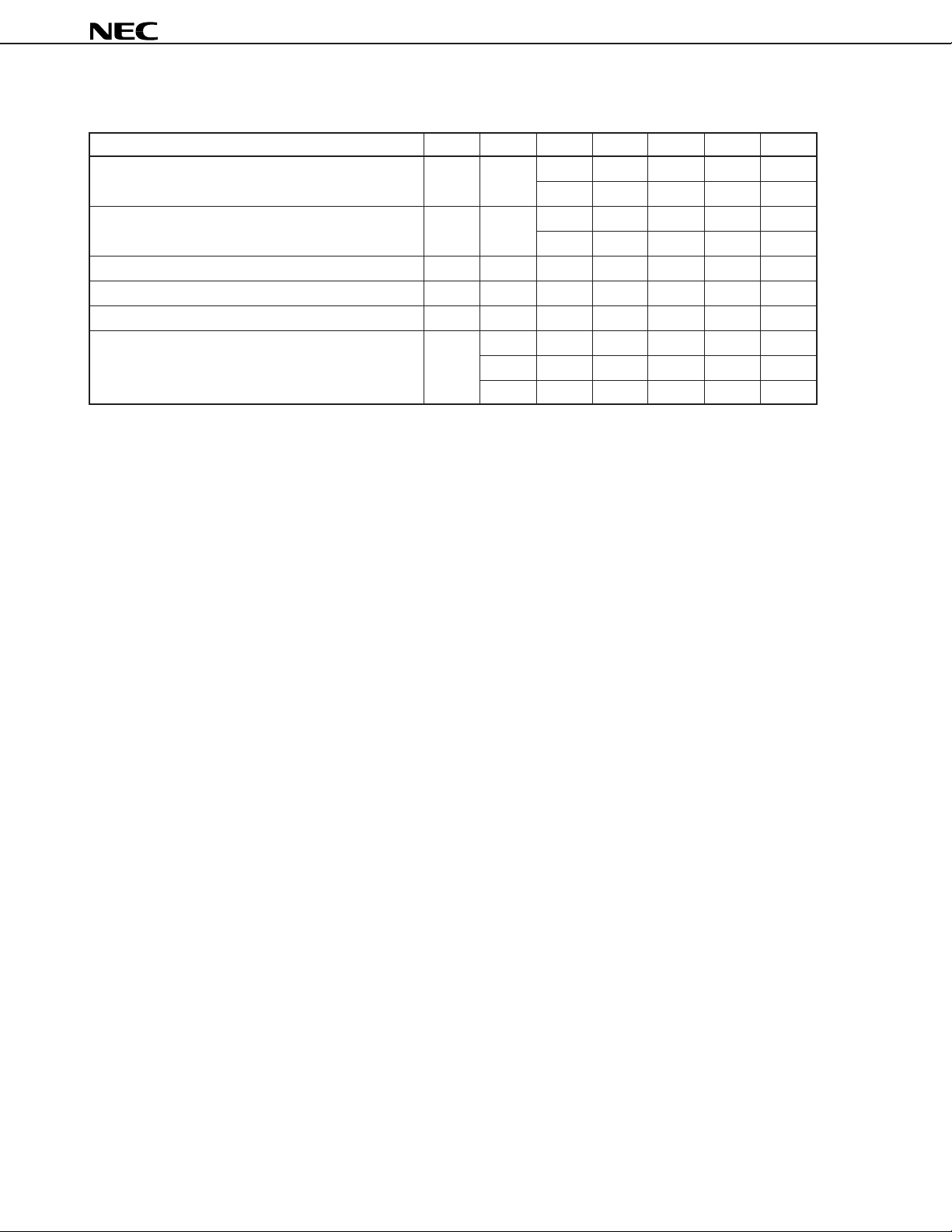
INPUT PIN CAPACITANCE (TA = +25 °C, VOD = 12 V)
Parameter Symbol Pin name Pin No. MIN. TYP. MAX. Unit
Shift register clock pin capacitance 1 C
Shift register clock pin capacitance 2 C
Last stage shift register clock pin capacitance C
Reset gate clock pin capacitance C
Reset feed-through level clamp clock pin capacitance C
Transfer gate clock pin capacitance C
Remark Pins 9 and 15 (φ1), 10 and 16 (φ2) are each connected inside of the device.
φ
1
φ
1 9 500 800 pF
15 500 800 pF
φ
2
φ
2 10 500 800 pF
16 500 800 pF
φ
L
φ
1L 19 50 pF
φ
RB
φ
RB 6 50 p F
φ
CLB
φ
CLB 20 50 pF
φ
TG
φ
TG1 14 70 pF
φ
TG2 13 70 pF
φ
TG3 11 70 pF
µ
PD3729
6
 Loading...