NEC UPC1851BCU Datasheet

DATA SHEET
BIPOLAR ANALOG INTEGRATED CIRCUIT
µ
PC1851B
I2C BUS-COMPATIBLE US MTS PROCESSING LSI
The µPC1851B is an integrated circuit for US MTS (Multiplexed Television Sound) system with the addition of
2
C bus interface. All functions required for US MTS system are incorporated on a single chip.
the I
The µPC1851B allows users to switch modes, control volume and tone, and adjust the separation circuit
through the I2C bus.
FEATURES
• Stereo demodulation, SAP (Sub Audio Program) demodulation, dbx noise reduction decoding, I2C bus interface,
input selector (2 channels), surround processor (1 phase), volume and tone control circuits incorporated on a single
chip
2
• Mode switching, volume and tone control, and separation adjustment through the I
• Power supply: 8 V to 10 V
• On-chip input attenuator for simple interface with intermediate frequency processing IC (I
• Output level: 1.4 Vp-p (with L+R signals, 100 % modulation)
C bus
2
C bus control)
APPLICATION
• TV sets and VCRs for north America
ORDERING INFORMATION
Part Number Package
µ
PC1851BCU 42-pin plastic SDIP (15.24 mm (600))
The µPC1851B is available only to licensees of THAT Corporation.
For information, please call: (508) 229-2500 (U.S.A), or (03) 5790-5391 (Tokyo).
The information in this document is subject to change without notice. Before using this document, please
confirm that this is the latest version.
Not all devices/types available in every country. Please check with local NEC representative for availability
and additional information.
Document No. S13417EJ2V0DS00 (2nd edition)
Date Published June 2000 N CP(K)
Printed in Japan
The mark shows major revised points.
©
1998
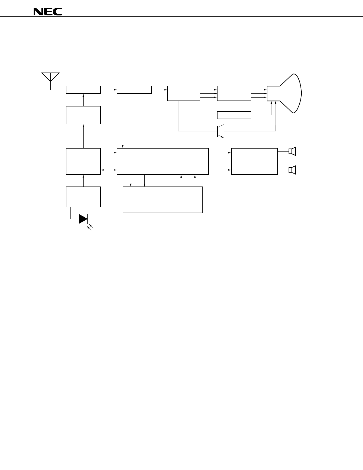
SYSTEM BLOCK DIAGRAM
● TV
µ
PC1851B
Tuner
DTS
interface
Tuning
microcontroller
Remote
controller
receive amp.
PIN photodiode
IF processing
PC1851B
µ
SCL
MTS processing
SDA R
LLRR
Graphic equalizer
(Surround processor)
C, Y, and
deflecting
signal output
Chroma output
Vertical output
L
Power amplifier
CRT
2
Data Sheet S13417EJ2V0DS00
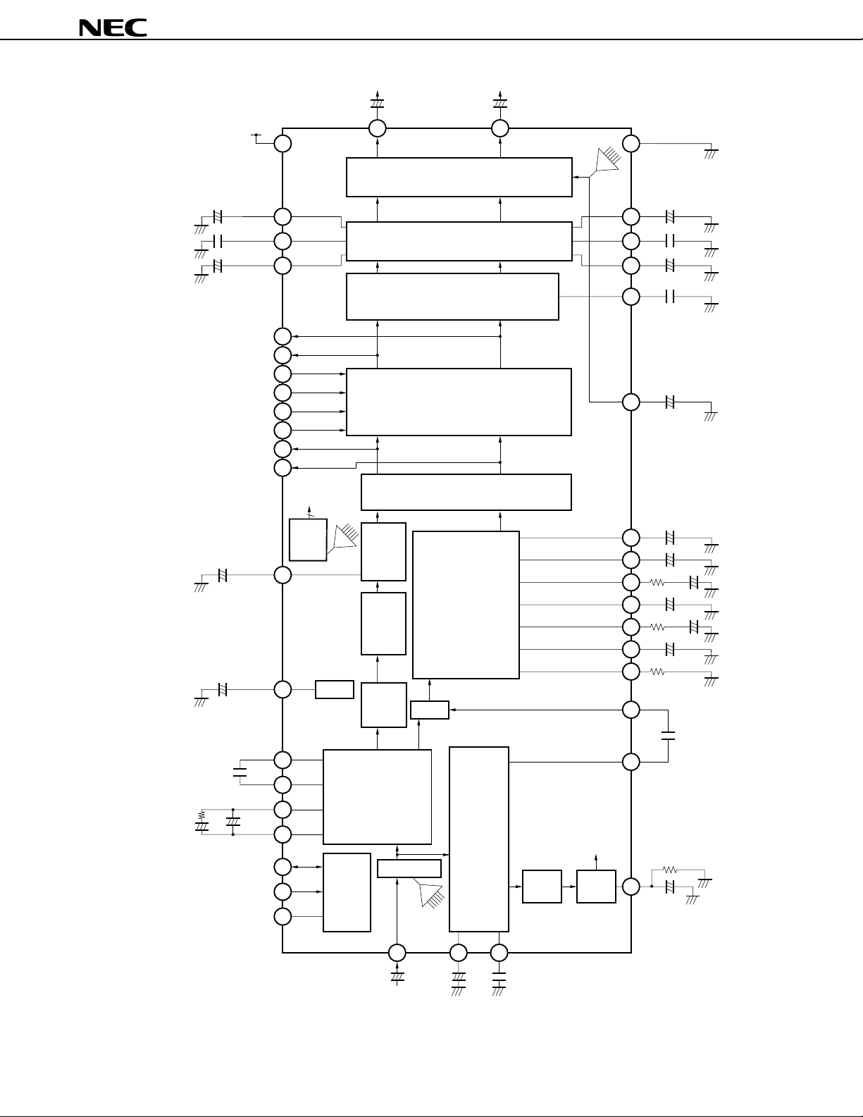
µ
PC1851B
BLOCK DIAGRAM
µ
2.2 F
+
2200 pF
0.1 F
µ
+
9 V
V
TLO
LTC
LBC
FOR
FOL
EL2
EL1
ER2
ER1
MOL
MOR
10 F
+
LOT
26
1
CC
ROT
25
10 F
µµ
+
21
AGND
D/A
Volume Control
2.2 F
µ
31
32
33
Tone Control
Surround Block
28
29
30
27
TRO
RTC
RBC
SUR
+
2200 pF
0.1 F
µ
+
0.022 F
µ
40
41
37
4.7 F
VOL-C
µ
+
39
36
Selector Block
19
38
35
34
Filter
Matrix Block
1 kΩ
+
4.7 F
22 F
0.1 F
µ
1 F
µ
µ
µ
1 F
µ
+
+
+
DGND
MOA
VRE
PD2
PD1
φ
D1
φ
D2
SDA
SCL
42
2
4
3
5
6
22
23
24
Filter
Control
D/A
1/2V
I2C Bus
Interface
CC
Offset
Absorption
De-
emphasis
L+R
LPF
Stereo
Demodulation
Block
Input Attenuator
dbx Noise
Reduction Block
Switch
Demodulation
D/A
SAP
Block
Noise
BPF
I2C Bus
Interface
Noise
Detector
20
16
17
13
14
18
15
11
10
µ
1 F
VOA
10 F
µ
WTI**
WRB
STI**
SRB
dO
5.1 kΩ
3.3 F
+++
3 kΩ
1 F
+
16.6 kΩ
µ
1 F
+
µ
µ
1
F
+
µ
ITI*
SI
µ
0.1
F
SOT
68 k
Ω
+
9
NDT
µ
0.47 F
COM
7
+
2.2 F
SOA
12
SDT
+
0.1 F
8
0.047 F
µ µ µ
Remark Use the followings for external parts.
Resistor (*): Metal film resistor (± 1 %). Unless otherwise specified; ±5 %
Capacitors (**): Tantalum capacitor (±10 %). Unless otherwise specified; ±20 %
Data Sheet S13417EJ2V0DS00
3
STEREO DEMODULATION BLOCK
D2
φ
D1
φ
5
Stereo Phase
Comparator
6
PD14PD2
3
Pilot Discrimination
Phase Comparator
2
C bus Interface
To I
D/A
Stereo
VCO
µ
PC1851B
Divider
1
4
1
2
From Input Attenuator
Stereo LPF
SAP DEMODULATION BLOCK
From Input Attenuator
To Noise BPF
SOA
12
8SDT
Offset Absorption
To I2C bus Interface
SAP BPF
SAP Detector
Pilot Canceler
Phase Detector
L–R AM
Demodulator
To L+R LPF
Loop Filter SAP VCO
To Switch
SAP LPF
D/A
10
SOT
4
Data Sheet S13417EJ2V0DS00
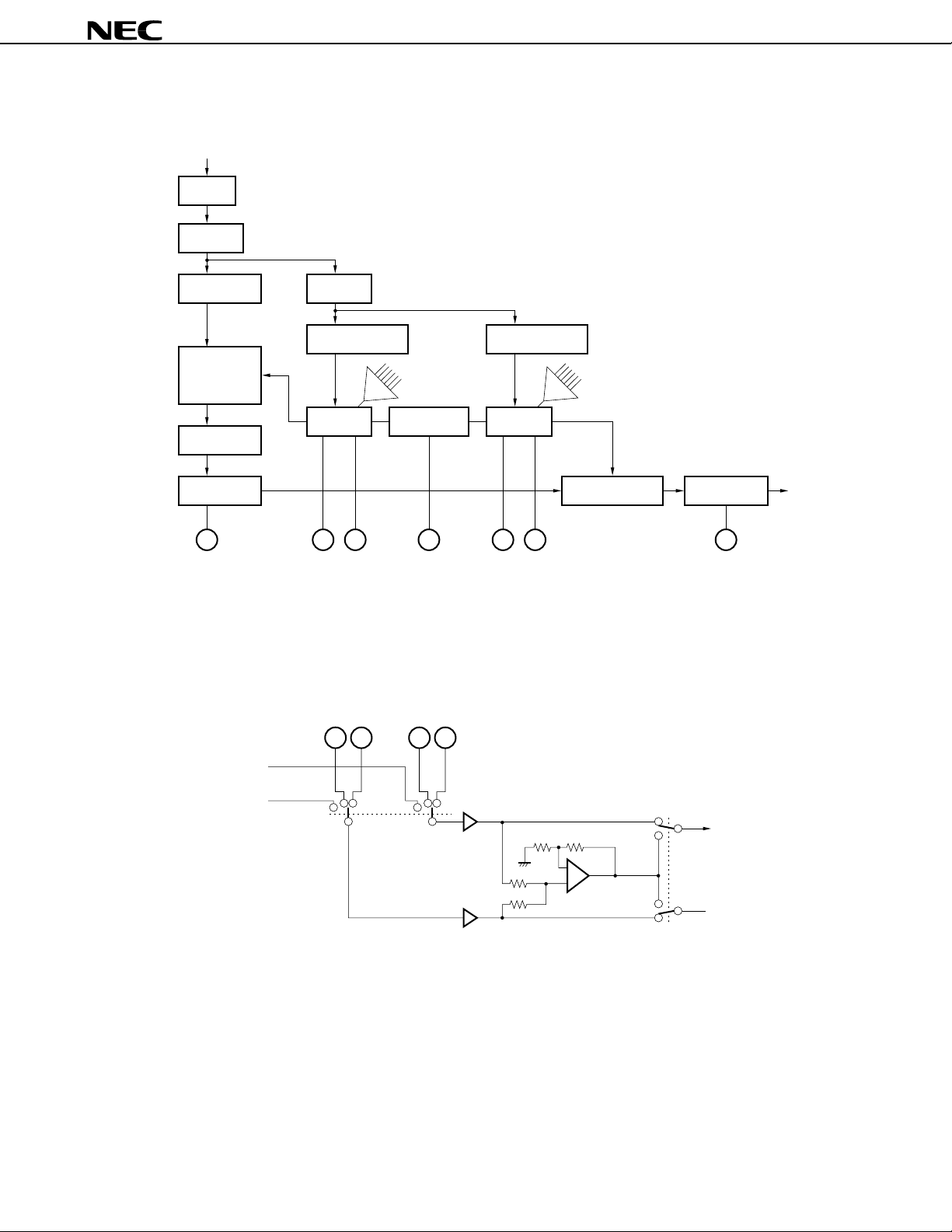
dbx NOISE REDUCTION BLOCK
From Switch
LPF
fH Trap
µ
PC1851B
408-Hz LPF
Variable
Emphasis
2.19-kHz LPF
Offset
Absorption
18
dO
SELECTOR BLOCK
2 fH Trap
Spectral RMS Filter
Spectral
RMS
14
SRB13STI
ER136ER2
38
Timing Current
15
ITI
EL137EL2
39
Wide-band RMS
Filter
D/AD/A
Wide-band
RMS
Wide-band VCA
16
17
WTI
WRB
Offset
Absorption
20
VOA
To Matrix Block
From Matrix Block
(L-channel signal)
From Matrix Block
(R-channel signal)
Switch
Note1
Note2
Note2
40 kΩ 40 kΩ
40 kΩ
40 kΩ
Notes 1. Switch (TV signal/External input 1/External input 2).
2. The input gain 0 dB/6 dB can be selected by the command of the I
Data Sheet S13417EJ2V0DS00
To Surround Block
–
+
2
C bus (refer to 4.3 (5) Input gain).
Switch (Monaural/Stereo)
To Surround Block
5
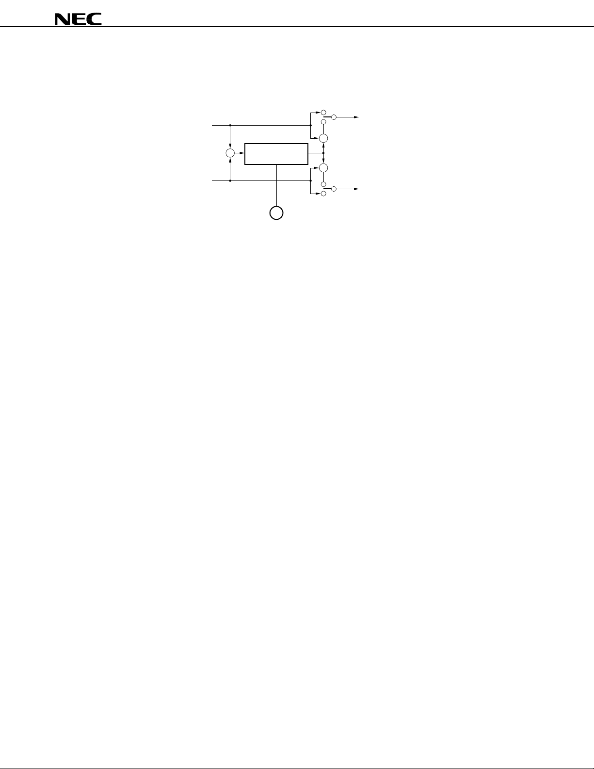
SURROUND BLOCK
µ
PC1851B
From Selector Block
(L-channel)
From Selector Block
(R-channel)
–
To Tone Control Block
–
Phase Shifter
+
To Tone Control Block
27
SUR
6
Data Sheet S13417EJ2V0DS00
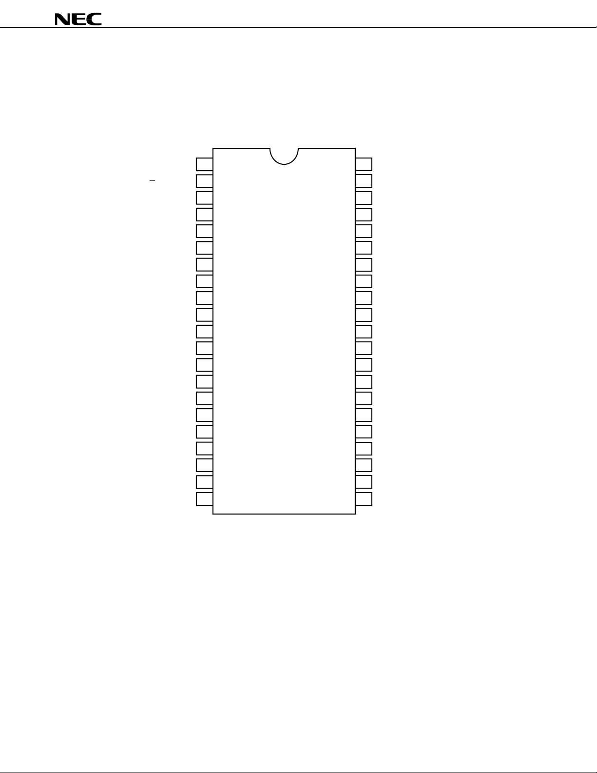
PIN CONFIGURATION (Top View)
42-pin plastic SDIP (15.24 mm (600))
• µPC1851BCU
µ
PC1851B
Power Supply (9 V)
1
Vcc Filter
2
Pilot Discrimination Filter 1
Pilot Discrimination Filter 2
Phase Comparator Filter 1
Phase Comparator Filter 2
Composite Signal Input
SAP Discrimination Filter
Noise Detector Filter
SAP Single Output
SAP Single Input
SAP Offset Absorption
Spectral RMS Timing
Spectral RMS Offset Absorption
Timing Current Setting
Wide-band RMS Timing
Wide-band RMS Offset Absorption
10
11
12
13
14
15
16
17
V
CC
1
VRE
2
PD1
3
PD2
4
φ
D1
5
φ
D2
6
COM
7
SDT
8
NDT
9
SOT
SI
SOA
STI
SRB
ITI
WTI
WRB
MOA
FOL
FOR
EL1
ER1
EL2
ER2
MOL
MOR
LBC
LTC
TLO
RBC
RTC
TRO
SUR
LOT
42
Monaural Offset Absorption
41
L-channel Fixed Output
40
R-channel Fixed Output
39
External L-channel Input 1
38
External R-channel Input 1
37
External L-channel Input 2
36
External R-channel Input 2
35
L-channel Matrix Output
34
R-channel Matrix Output
33
L-channel Capacity of Low Frequency Band Width
32
L-channel Capacity of High Frequency Band Width
31
L-channel Offset Absorption
30
R-channel Capacity of Low Frequency Band Width
29
R-channel Capacity of High Frequency Band Width
28
R-channel Offset Absorption
27
Surround Timing
26
L-channel Output
Variable Emphasis Offset Absorption
Volume Control Offset Absorption
VCA Offset Absorption
Analog GND
18
19
20
21
dO
VOL-C
VOA
AGND
ROT
DGND
SCL
SDA
25
R-channel Output
24
Digital GND (for I
SCL (for I
23
SDA (for I
22
2
C bus)
2
C bus)
2
C bus)
Data Sheet S13417EJ2V0DS00
7

CONTENTS
1. PIN EQUIVALENT CIRCUITS............................................................................................ 9
2. BLOCK FUNCTIONS........................................................................................................ 18
2.1 Stereo Demodulation Block................................................................................... 18
2.2 SAP Demodulation Block ...................................................................................... 19
2.3 dbx Noise Reduction Block ................................................................................... 20
2.4 Matrix Block............................................................................................................ 21
2.5 Selector Block ........................................................................................................ 21
2
C BUS INTERFACE ....................................................................................................... 22
3. I
3.1 Data Transfer ......................................................................................................... 23
3.2 Data Transfer Format ............................................................................................ 24
2
C BUS COMMANDS ...................................................................................................... 27
4. I
4.1 Subaddress List ..................................................................................................... 27
4.2 Setting Procedure .................................................................................................. 29
4.3 Explanation of Write Register ................................................................................ 31
4.4 Explanation of Read Register ............................................................................... 38
µ
PC1851B
5. MODE MATRIX ................................................................................................................. 4 0
6. SELECTOR TABLE.......................................................................................................... 41
7. USAGE CAUTIONS.......................................................................................................... 42
7.1 Caution on Shock Noise Reduction ...................................................................... 42
7.2 Supply Voltage....................................................................................................... 42
7.3 Impedance of Input and Output Pins .................................................................... 42
7.4 Drive Capability of Output Pins ............................................................................. 42
7.5 Caution on External Components ......................................................................... 43
7.6 Change of Electrical Characteristics by External Components........................... 43
8. ELECTRICAL SPECIFICATIONS.................................................................................... 44
9. TEST CIRCUIT.................................................................................................................. 56
10. PACKAGE DRAWINGS ................................................................................................... 58
11. RECOMMENDED SOLDERING CONDITIONS .............................................................. 59
8
Data Sheet S13417EJ2V0DS00
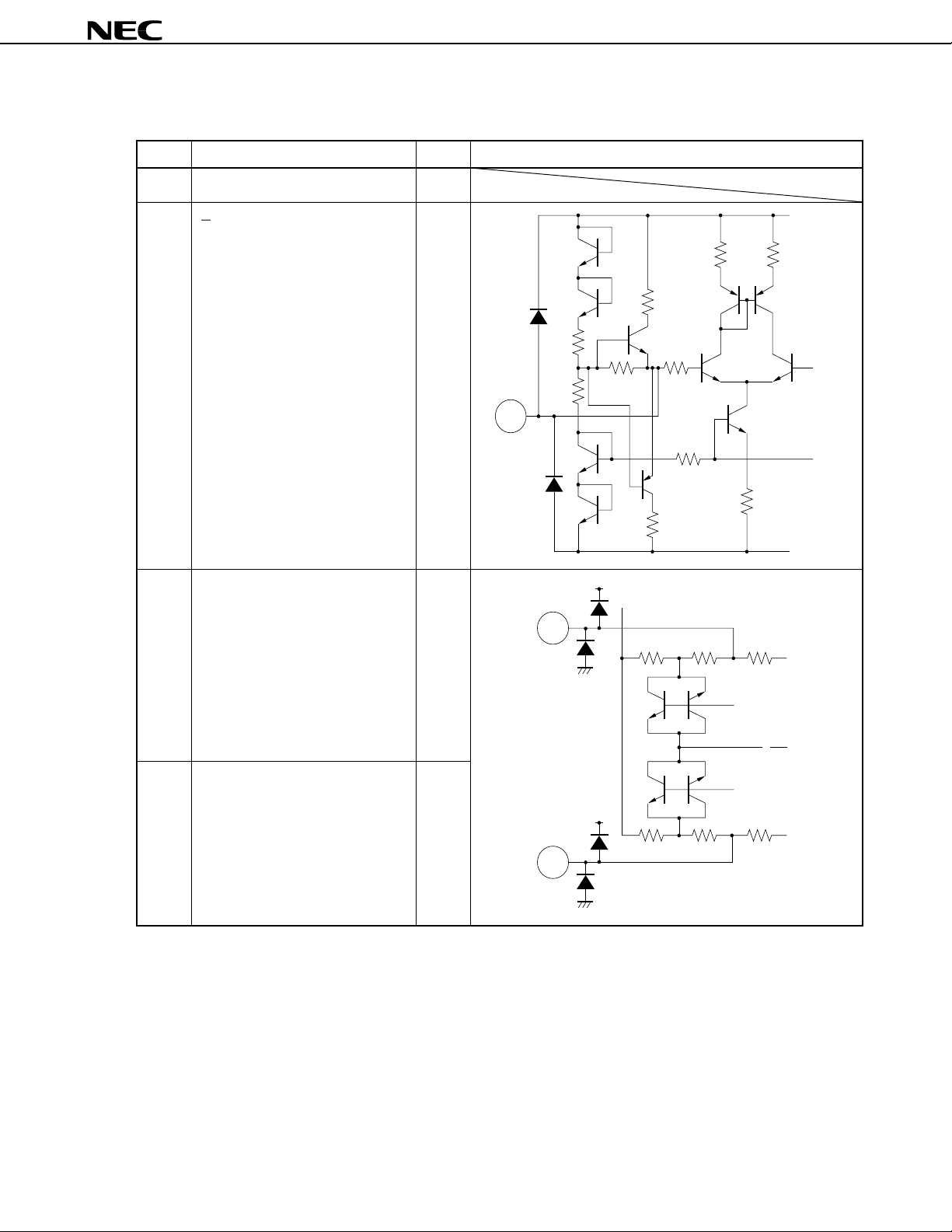
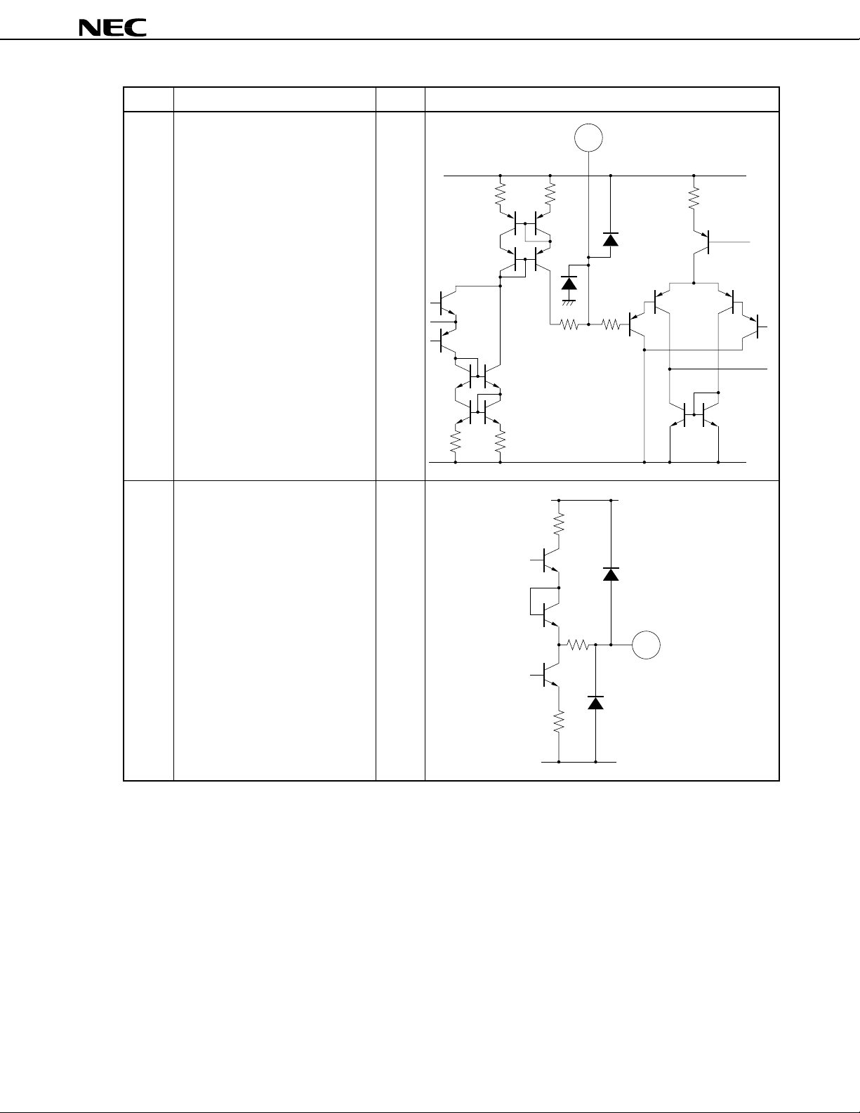
1. PIN EQUIVALENT CIRCUITS
Pin No. Pin Name Symbol Internal Equivalent Circuit
1 Power Supply (9 V) VCC
µ
PC1851B
(1/9)
1
2 VCC Filter VRE
2
3 Pilot Discrimination Filter 1 PD1
VCC
10 kΩ 10 kΩ
5 kΩ
20 kΩ
20 kΩ
20 kΩ
10 kΩ
2
10 kΩ
20 kΩ
5 kΩ
GND
V
CC
3
15 kΩ 5 kΩ
15 kΩ
4 Pilot Discrimination Filter 2 PD2
1
CC
V
2
V
CC
4
15 kΩ15 kΩ 5 kΩ
Data Sheet S13417EJ2V0DS00
9
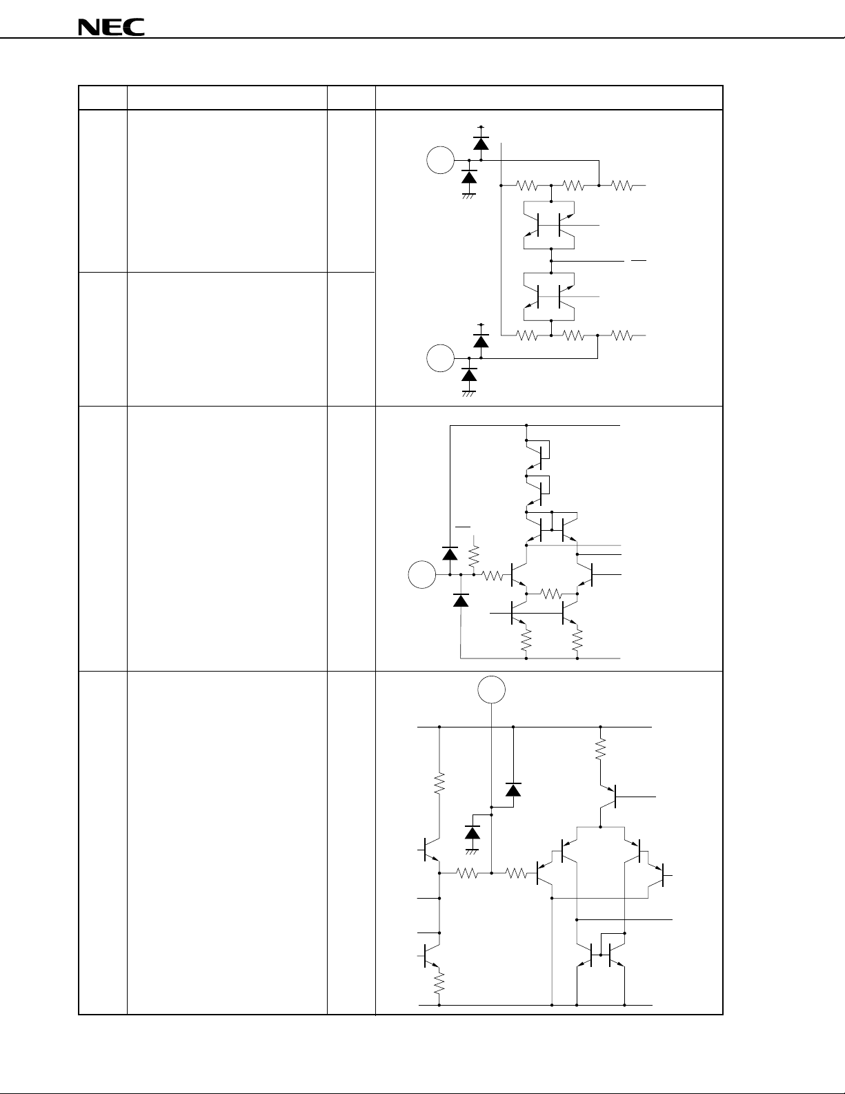
Pin No. Pin Name Symbol Internal Equivalent Circuit
µ
PC1851B
(2/9)
5 Phase Comparator Filter 1
6 Phase Comparator Filter 2
φ
D1
φ
D2
7 Composite Signal Input COM
V
CC
5
15 kΩ 5 kΩ
V
CC
6
1
V
CC
2
5 kΩ
5 kΩ15 kΩ 5 kΩ
1
V
CC
2
CC
V
80 kΩ
7
3 kΩ
17 kΩ
8 SAP Discrimination Filter SDT
5 kΩ 5 kΩ
GND
8
VCC
20 kΩ
10 kΩ
20 kΩ20 kΩ
10 kΩ
GND
10
Data Sheet S13417EJ2V0DS00
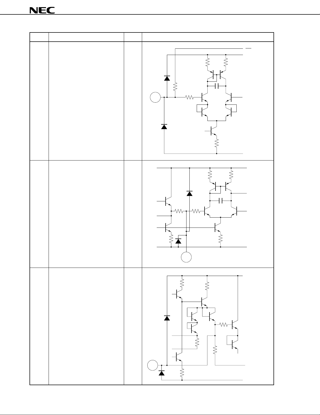
Pin No. Pin Name Symbol Internal Equivalent Circuit
µ
PC1851B
(3/9)
9 Noise Detector Filter NDT
10 SAP Single Output SOT
20 kΩ20 kΩ
20 kΩ 20 kΩ
2 kΩ
9
V
CC
20 kΩ
20 kΩ20 kΩ
GND
V
CC
2 kΩ
200 Ω
10
GND
Data Sheet S13417EJ2V0DS00
11
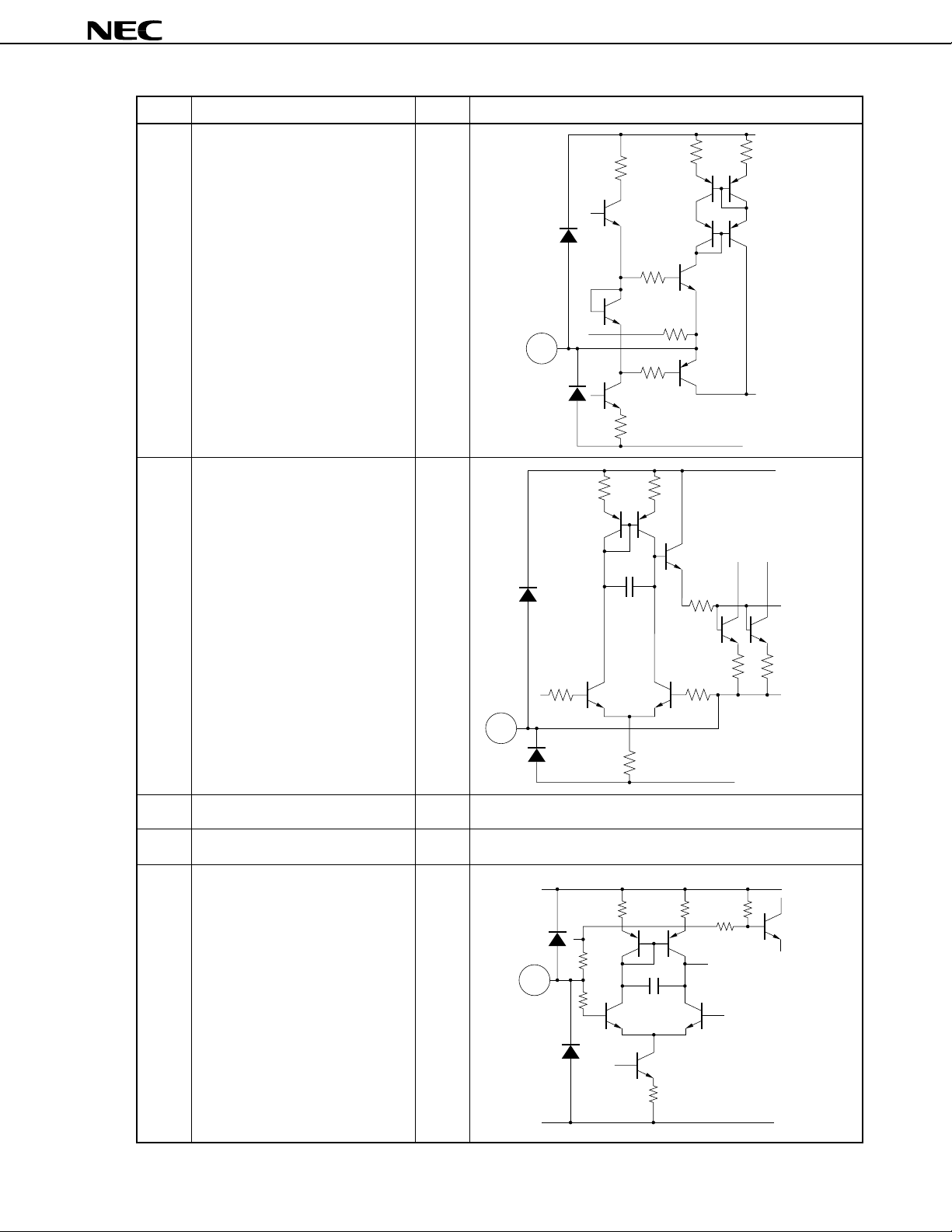
Pin No. Pin Name Symbol Internal Equivalent Circuit
11 SAP Single Input SI
10 kΩ 10 kΩ
80 kΩ
11
5 kΩ
5 pF
5 kΩ
1
2
V
CC
GND
µ
V
CC
PC1851B
(4/9)
12 SAP Offset Absorption SOA
13 Spectral RMS Timing STI
12
5 kΩ
V
CC
10 kΩ10 kΩ
5 pF
3 kΩ50 kΩ
10 kΩ2.3 kΩ
GND
V
CC
600 Ω
12
5 kΩ
5 kΩ
5 kΩ
13
5 kΩ
GND
Data Sheet S13417EJ2V0DS00
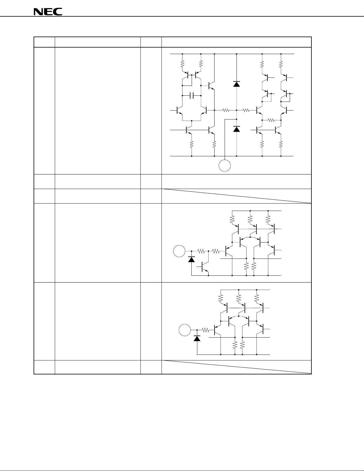
Pin No. Pin Name Symbol Internal Equivalent Circuit
14 Spectral RMS Offset Absorption SRB
5 kΩ
3 kΩ
5 kΩ 5 kΩ
3 kΩ
µ
PC1851B
V
CC
(5/9)
15 Timing Current Setting ITI
15
14
10 kΩ 10 kΩ
10 kΩ
5 kΩ
20 pF
3 kΩ
30 kΩ
5 kΩ
10 kΩ
10 kΩ
GND
10
kΩ
GND
V
CC
16 Wide-band RMS Timing WTI Same as pin 13
17 Wide-band RMS Offset Absorption WRB Same as pin 14
18 Variable Emphasis Offset dO
Absorption
Data Sheet S13417EJ2V0DS00
V
GND
CC
18
50 k
3 kΩ
Ω
10 kΩ 10 kΩ
20 kΩ
6 pF
10 kΩ
20 k
Ω
13
Pin No. Pin Name Symbol Internal Equivalent Circuit
µ
PC1851B
(6/9)
19 Volume Control Offset Absorption VOL-C
10 kΩ10 kΩ
5 pF
20 kΩ
20 VCA Offset Absorption VOA Same as pin 12
21 Analog GND AGND
22 SDA (for I2C bus)
Note
SDA
10 kΩ
5 kΩ
5 kΩ5 kΩ
10 kΩ 10 kΩ
19
10 kΩ 10 kΩ 10 kΩ
25 kΩ
5 kΩ
V
CC
V
CC
GND
23 SCL (for I2C bus)
24 Digital GND (for I2C bus) DGND
Note
SCL
22
50 kΩ5 k
23
5 k
Ω
30 k
10 kΩ 10 kΩ 10 kΩ
Ω
30 k
Ω
30 k
Ω
30 k
Ω
GND
V
CC
Ω
GND
Note A protection diode on the VCC side is deleted not so as to pull the voltage of I2C bus line down to 0 V while
the power supply is off (VCC = 0 V).
14
Data Sheet S13417EJ2V0DS00
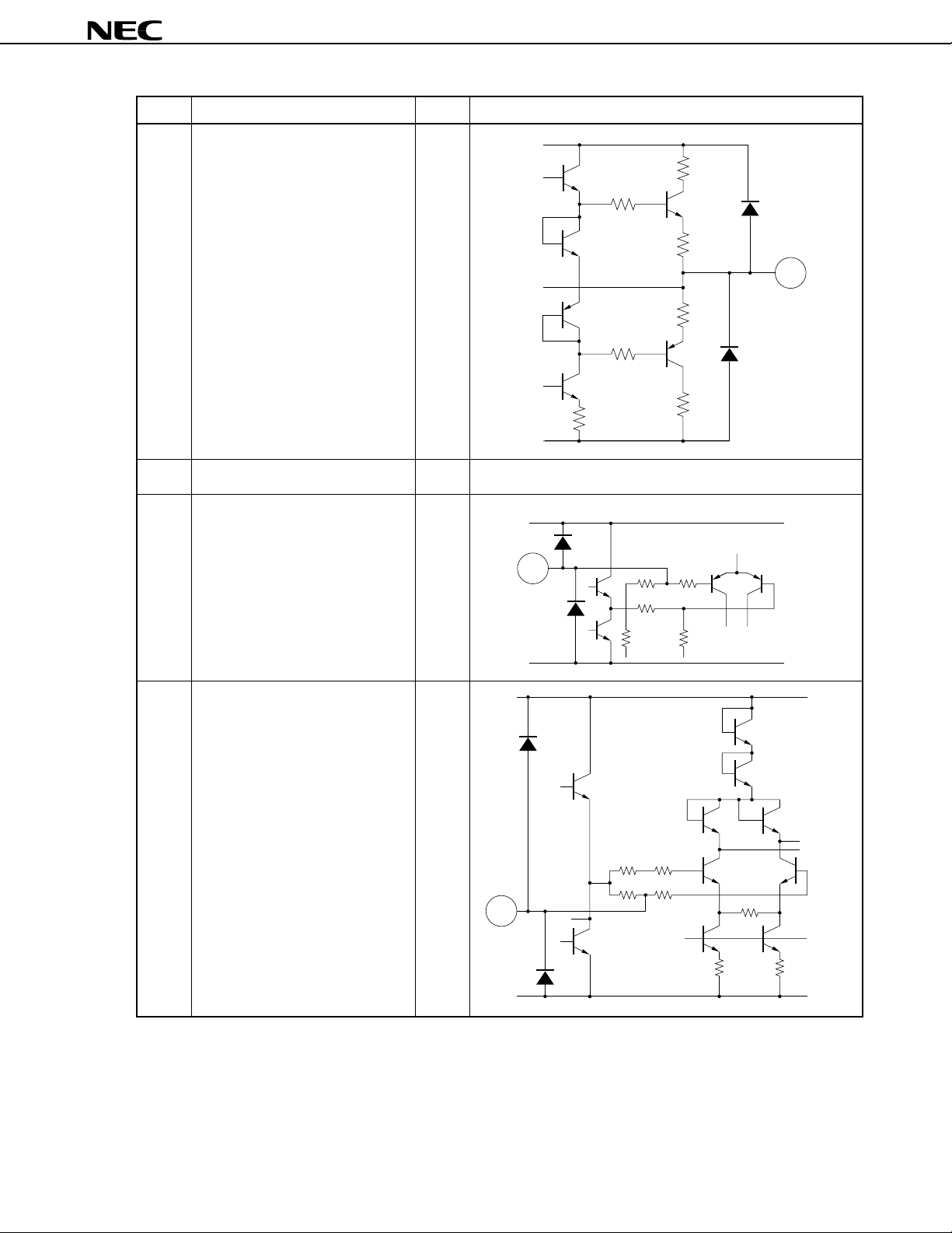
Pin No. Pin Name Symbol Internal Equivalent Circuit
µ
PC1851B
(7/9)
25 R-channel Output ROT
5 kΩ
26 L-channel Output LOT Same as pin 25
27 Surround Timing SUR
27
10 kΩ
5 kΩ
200 Ω
200Ω
1 kΩ
2 kΩ
1 kΩ
GND
VCC
25
V
CC
28 R-channel Offset Absorption TRO
28
24 kΩ
20 kΩ
20 kΩ40 kΩ
GND
VCC
35 kΩ 5 kΩ
35 kΩ 5 kΩ
40 kΩ
10 kΩ10 kΩ
GND
Data Sheet S13417EJ2V0DS00
15
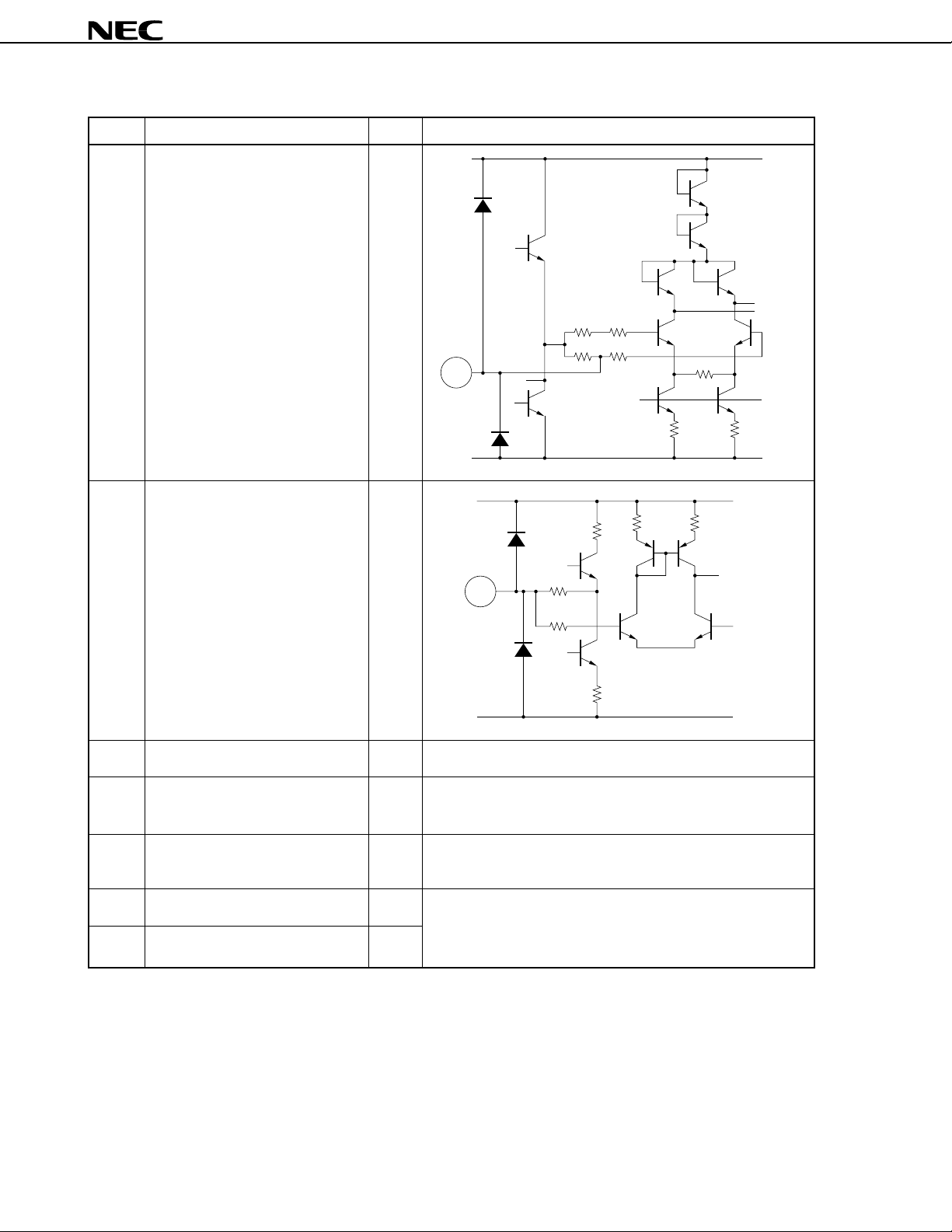
Pin No. Pin Name Symbol Internal Equivalent Circuit
µ
PC1851B
(8/9)
29 R-channel Capacity of High RTC
Frequency Band Width
30 R-channel Capacity of Low RBC
Frequency Band Width
29
30
1 kΩ
5.3 kΩ
3 kΩ
36 kΩ 5 kΩ
36 kΩ 5 kΩ
40 kΩ
10 kΩ 10 kΩ
5 kΩ
5 kΩ
VCC
GND
V
CC
31 L-channel Offset Absorption TLO Same as 28
32 L-channel Capacity of High LTC Same as 29
Frequency Band Width
33 L-channel Capacity of Low LBC Same as 30
Frequency Band Width
34 R-channel Matrix Output MOR Same as 25
35 L-channel Matrix Output MOL
2.5 kΩ
GND
16
Data Sheet S13417EJ2V0DS00
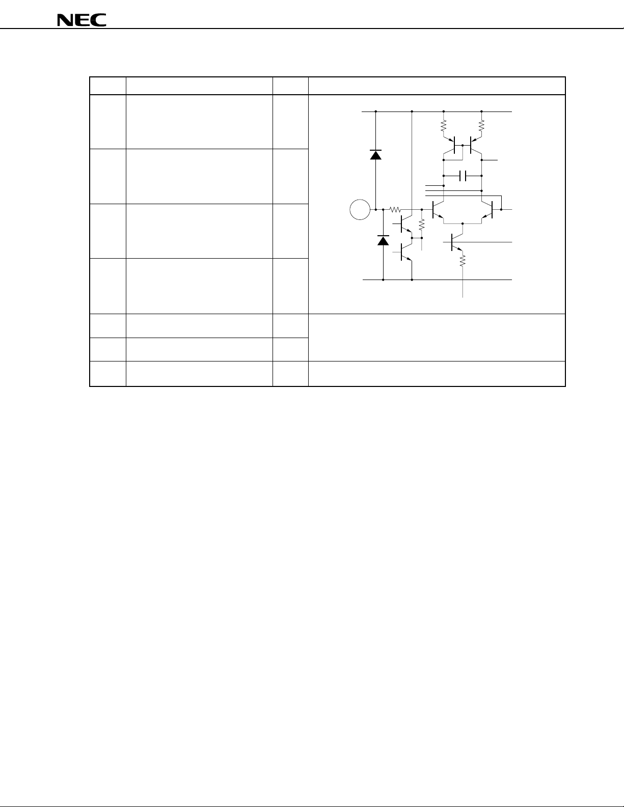
Pin No. Pin Name Symbol Internal Equivalent Circuit
36 External R-channel Input 2 ER2
37 External L-channel Input 2 EL2
15 pF
40 kΩ
38 External R-channel Input 1 ER1
36
40 kΩ
µ
PC1851B
10 kΩ10 kΩ
(9/9)
39 External L-channel Input 1 EL1
40 R-channel Fixed Output FOR Same as pin 25
41 L-channel Fixed Output FOL
42 Monaural Offset Absorption MOA Same as pin 18
2
I
C Bus
10 kΩ
Data Sheet S13417EJ2V0DS00
17

µ
PC1851B
2. BLOCK FUNCTIONS
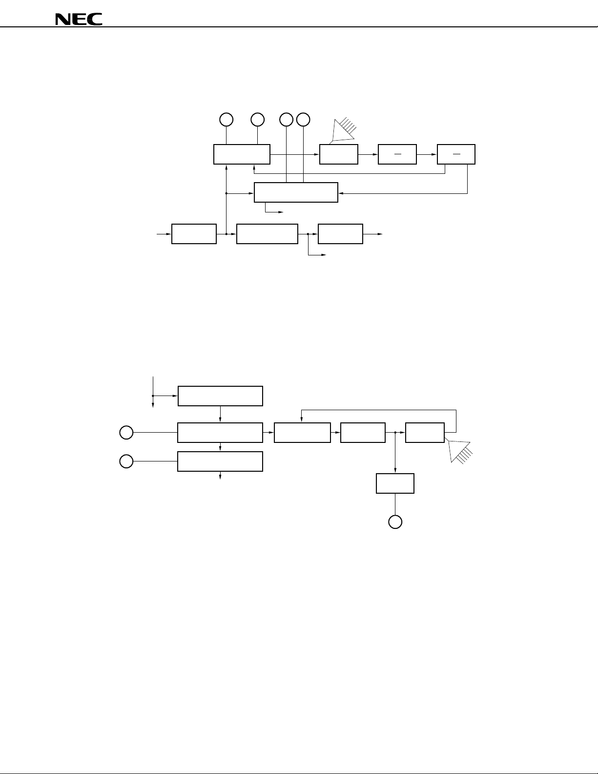
2.1 Stereo Demodulation Block
(1) Stereo LPF
This filter eliminates signals in the vicinity of 5 fH to 6 fH, such as SAP (Sub Audio Program) (5 fH) and telemetry
signals (6.5 f
L–R signals by multiplication of the L–R signal with the signal at the L–R carrier frequency (2 fH). The L–R signal
tends to receive interference from the 6 fH signal because a square waveform is used as the switching carrier in this
method. To eliminate this interference, the
adjusted by setting the FILTER SETTING bits (Write register, subaddress 02H, bits D0 to D5).
H) . The
µ
PC1851B’s internal L–R demodulator, which uses a double-balanced circuit, demodulates
µ
PC1851B incorporates traps at 5 fH and 6 fH. The filter response is
(2) Stereo Phase Comparator
The 8 fH signal generated at the Stereo VCO is divided by 8 (4 × 2) and then multiplied by the pilot signal passed
through the stereo LPF. The two signals differ from each other by 90 degrees in terms of phase.
The resistor and capacitor connected to the φD1 and φD2 pins form a filter that smoothes the phase error signal
output from the Stereo Phase Comparator, converting the error signal to the DC voltage. When the voltage difference
φ
between
8 fH.
D1 and φD2 pins becomes 0 V (strictly speaking, not 0 V by the internal offset voltage), the VCO runs at
φ
The lag/lead filter externally connected to the pins
D1 and φD2 determines the capture range.
(3) Stereo VCO
The Stereo VCO runs at 8 fH with the internal capacitor. The frequency is adjusted by setting the STEREO VCO
SETTING bits (Write register, subaddress 01H, bits D0 to D5).
(4) Divider (Flip-flop)
Produces two separate fH signals: the inphase fH signal, and the fH signal differing by 90 degrees from the input
pilot signal by dividing the 8 fH frequency from the Stereo VCO by 8 (4 × 2).
(5) Pilot Discrimination Phase Comparator (Level detector)
Multiplies the pilot signal from the COM pin with the inphase fH signal from the divider. The resulting signal is
smoothed by passing it through the external filter connected to the PD1 and PD2 pins and converted into DC
voltage that is used to determine whether or not a stereo pilot is present (Read register, bit D6).
(6) Pilot Canceler
The fH signal from the divider is added to the stereo signal matrix depending on the level of the input pilot signal
to cancel the pilot signal.
(7) L+R LPF
This LPF which has traps at fH and 24 kHz, allows only the monaural signal to pass through. The filter response
is adjusted by setting the FILTER SETTING bit (Write register, subaddress 02H, bits D0 to D5).
(8) De-emphasis
The 75-µs de-emphasis filter is for the monaural signal. The response is adjusted by setting the FILTER SETTING
bit (Write register, subaddress 02H, bits D0 to D5).
(9) L–R AM Demodulator
Demodulates the L–R AM-DSB modulated signal by multiplying with the 2-fH signal which is synchronized to the
pilot signal. The 2-fH square wave is used as the switching carrier.
18
Data Sheet S13417EJ2V0DS00
 Loading...