NEC UPC1830GT Datasheet

DATA SHEET
BIPOLAR ANALOG INTEGRATED CIRCUIT
µ
PC1830
FILTER-CONTAINING VIDEO CHROMA, SYNCHRONIZING SIGNAL
PROCESSING LSI COMPATIBLE WITH NTSC/PAL SYSTEM
DESCRIPTION
The µPC1830 is a filter-containing video chroma, synchronizing signal processing LSI compatible with the NTSC/
PAL system. A decoder which converts composite video or separate Y/C video signals into a brightness signal and
a color difference signal and outputs the result, and a matrix which comprises independent brightness signal/color
difference signal input pins are integrated on one chip.
Decoder output can be used to drive an A/D converter; it is appropriate for picture-in-picture screen signal
processing and multimedia boards.
FEATURES
• Contains a trap filter, band-pass filter, delay line, and color difference output low-pass filter.
Peripheral parts can be drastically reduced.
• Low power consumption
Appropriate for use with digital boards because of 5-V single power supply operation.
• DC control for user adjustment pins
Centralized control can be performed by a microcontroller.
• One chip compatible with both NTSC and PAL systems
Boards common to NTSC and PAL systems can be easily constructed.
• S pin input
Supports composite and separate Y/C video signal inputs.
• Demodulation ratio/demodulation angle change (matrix)
Demodulation ratio/demodulation angle can be selected in response to the NTSC or PAL system.
• Contains color difference tint control
Fine adjustment of the demodulation axis can be made for both the NTSC and PAL systems.
ORDERING INFORMATION
Part Number Package
µ
PC1830GT 42-pin plastic shrink SOP (375 mil)
The information in this document is subject to change without notice.
Document No. S11146EJ4V0DS00 (4th edition)
Date Published April 1998 N CP(K)
Printed in Japan
The mark shows major revised points.
©
1994
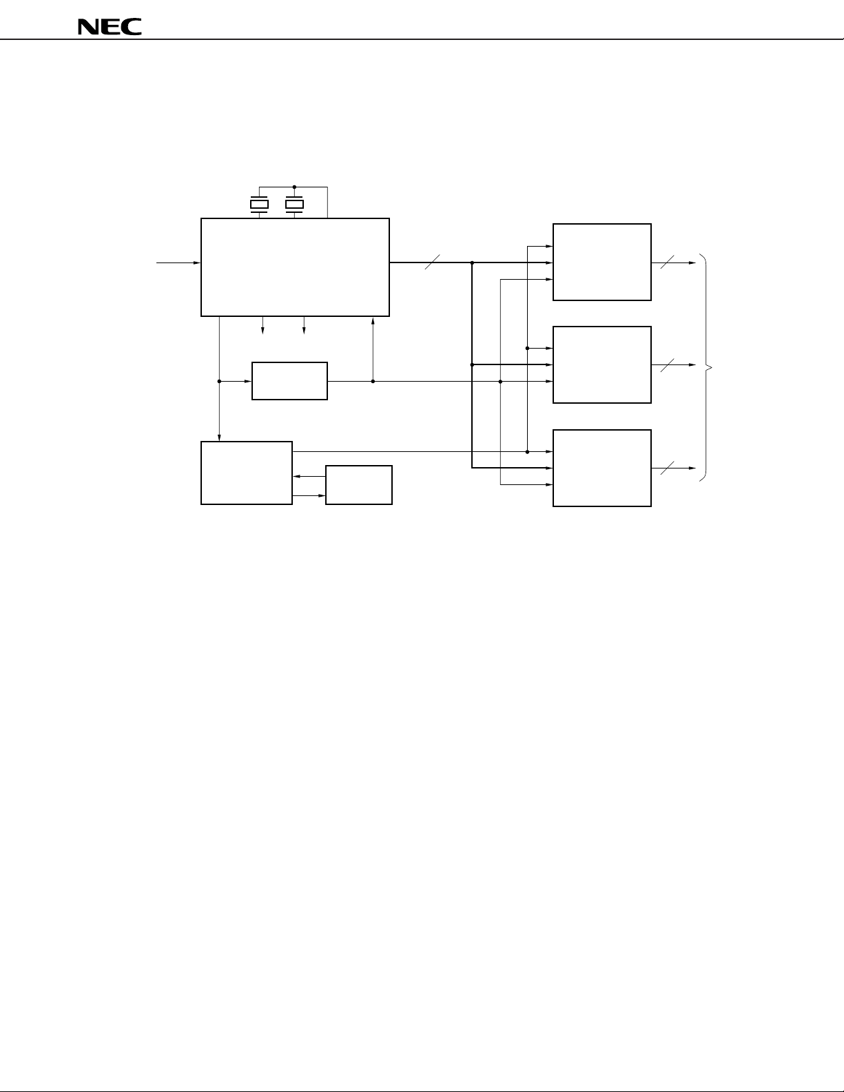
1. SYSTEM BLOCK DIAGRAM
VIDEO CAPTURE SYSTEM BLOCK DIAGRAM
NTSC
PAL
3.58
4.43
µ
PC1830
Composite video
or Y/C separate
signal input
RGB/Color
difference decoder
PC1830
µ
HD
VD BLK
H lock clock
generator
Clamp
pulse
Divider
CLP
910 f
RGB or YUV
H
8-bit A/D
µ
PC659A
8-bit A/D
µ
PC659A
8-bit A/D
µ
PC659A
8
8
8
Digital video (RGB or YUV) signal output
2
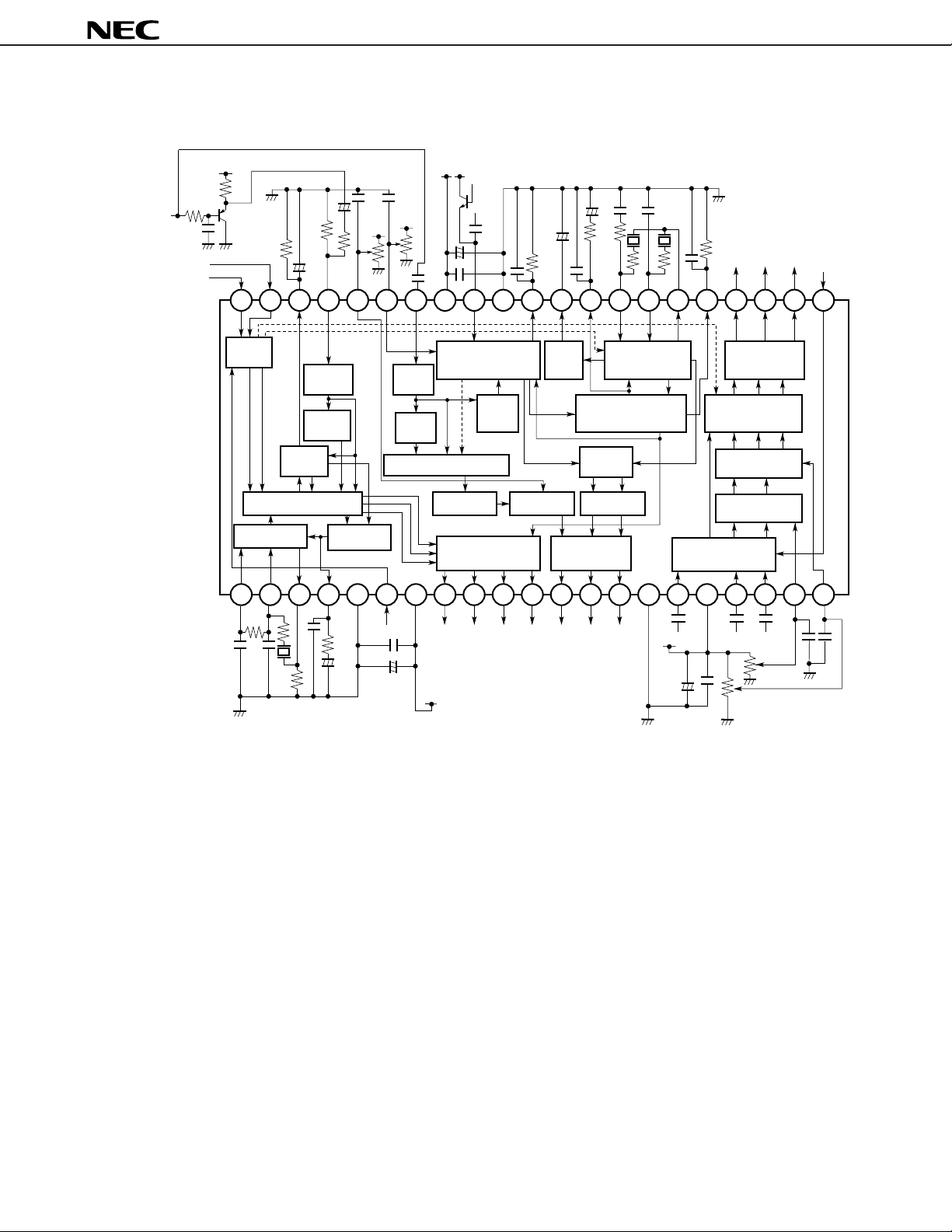
2. BLOCK DIAGRAM
V
CC
CVBS
3.58/4.43
NTSC/PAL
42 41 40 39 38 37 36 35 34 33 32 31 30 29 28 27 26 25 24 23 22
µ
PC1830
Separate/
V
CC
composite
Sub color
control
Contrast
+
control
V
CC
V
CC
+
switch
Separate
chroma
+
+
+
RGB
Clamp
pulse
Mode
switch
32 f
H/V count
H
VCO
Sync.
separate
V filter
H sync.
detect
H
V
AFC wave
detect
Clamp
chroma
Separate/composite switch
V
H
BLK
Separate/composite
switch, A
subcolor control
chroma
trap
Delay
HD, VD, blanking pulse,
killer output buffer
CC
amp.
BPF
Filter f
adjust
C
Contrast
control
Y
3.58 MHz/4.43 MHz
0
VCXO, PAL SW
APC, killer detect,
IDENT detect
Cf
R-Y, B-Y
modulate
Y, R-Y, B-Y
output buffer
R-Y B-Y
LPF
B-YR-YY
SC
Killer
f
SC
Y, R-Y, B-Y
input clamp
RGB output
buffer
RGB
NTSC/PAL
matrix
R-Y
B-Y
Tint control
B-Y
R-Y
Amp. color
control
R-Y B-Y
G-Y
1 2 3 4 5 6 7 8 9 10 11 12 13 14 15 16 17 18 19 20 21
50/60
+
Killer
BLK HD VD Y R-Y B-Y
detect
+
V
CC
V
CC
+
R-Y B-YY
Color
control
3

3. PIN CONFIGURATION (Top View)
42-pin plastic shrink SOP (375 mil)
µ
PC1830GT
µ
PC1830
H
VCO filter
32 f
H
VCO filter
32 f
H
VCO filter
32 f
Horizontal AFC filter
GND (synchronous section)
f
V
50/60 switch
Power supply (synchronous section)
Color killer output
Blanking pulse output
HD pulse output
VD pulse output
Y output
R-Y output
B-Y output
142
241
340
4 39
538
637
736
835
934
10 33
11 32
12 31
13 30
14 29
NTSC/PAL switch
SC
switch
f
H sync. detect filter
Sync. separation input
Contrast control
Subcolor control
Composite video signal input
Power supply (chroma section)
Separate chroma input
GND (chroma section)
ACC filter
fo adjustment filter
Chroma APC filter
SC
VCO input (4.43 MHz)
f
GND (video section)
Y input
Power supply (video section)
R-Y input
B-Y input
Color control
Tint control
15 28
16 27
17 26
18 25
19 24
20 23
21 22
f
SC
VCO input (3.58 MHz)
SC
VCO output
f
Color killer filter
B output
G output
R output
Clamp pulse input
4
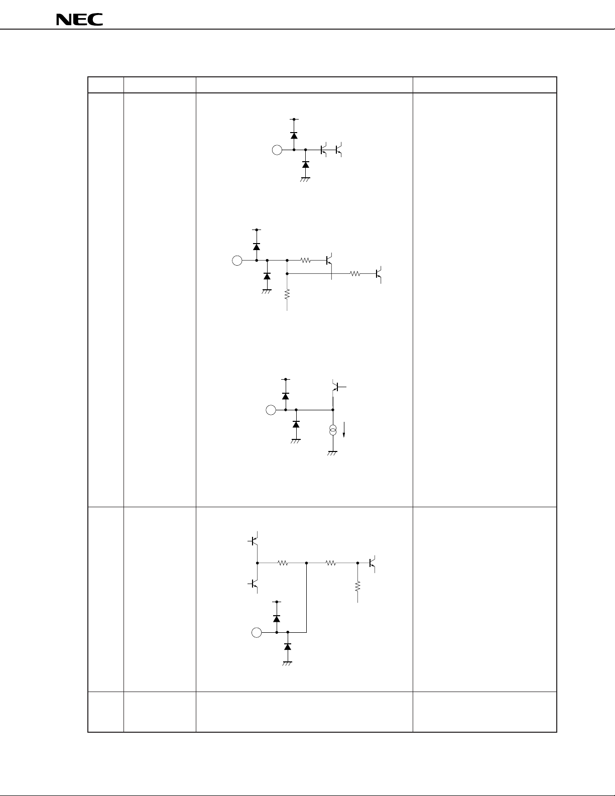
4. PIN EQUIVALENT CIRCUIT DIAGRAMS
µ
PC1830
Pin No. Pin name Equivalent circuit
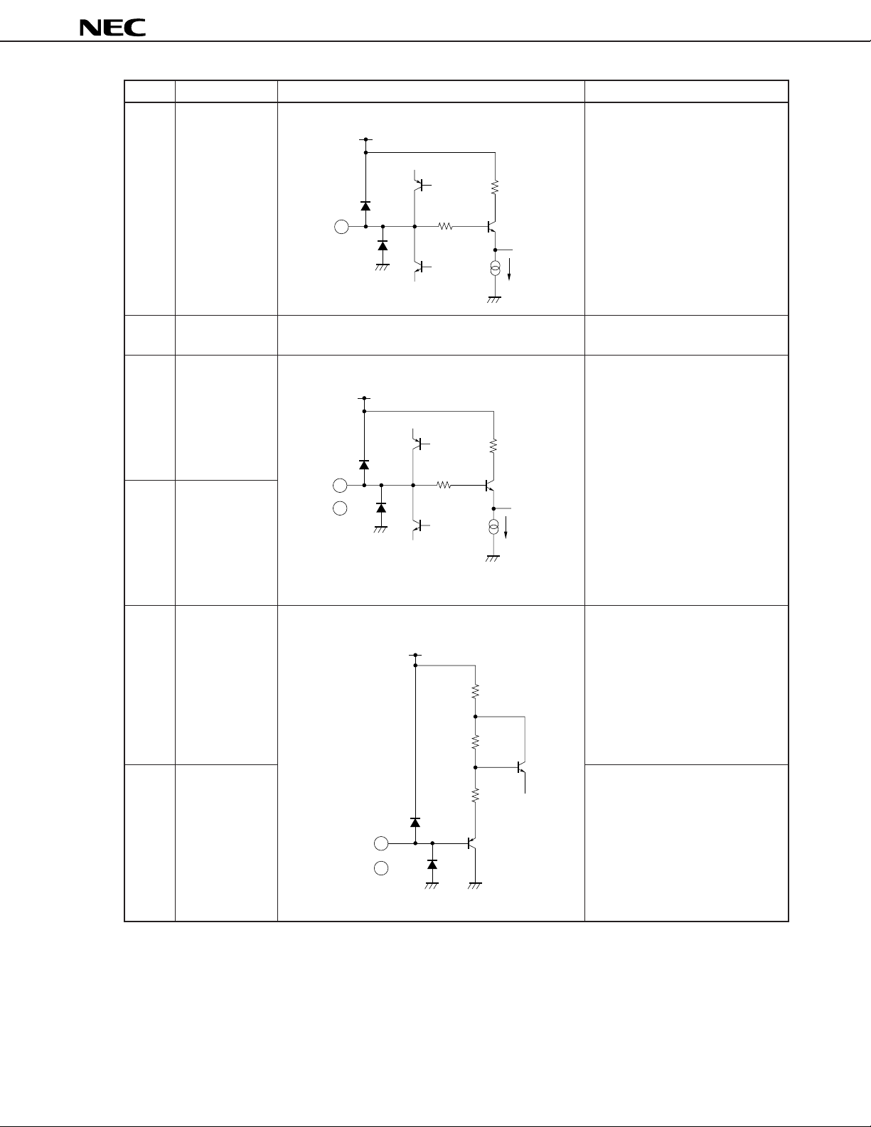
1 32 fH VCO filter
V
CC
2
3
2
1
V
CC
2.2 kΩ
3.3 kΩ
V
CC
Function descriptions
Pins for connecting a 32 fH
oscillation filter.
For resonator, use 500 kHz
ceramic resonator in both NTSC
and PAL modes. Bias of pin 1 is
supplied from pin 2 via an external
resistor between pins 1 and 2.
2.2 kΩ
4 Horizontal AFC
filter
5 GND
(synchronous
section)
3
1 mA
Pin for connecting filter of horizontal AFC detector.
300 Ω
CC
V
4
30 kΩ
3 kΩ
Synchronous section ground.
5
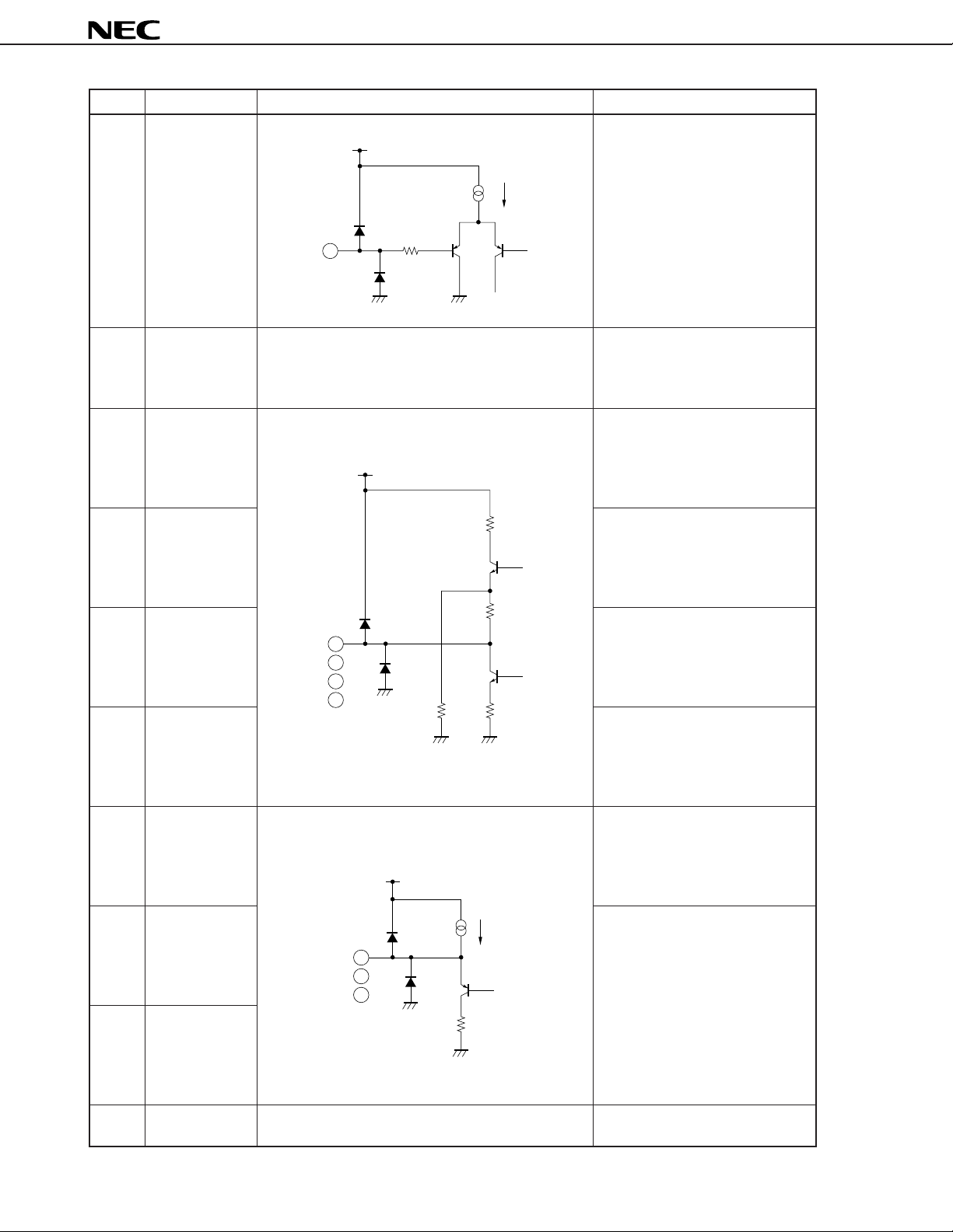
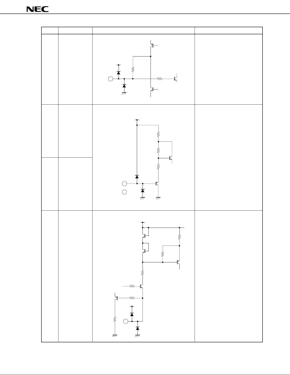
Pin No. Pin name Equivalent circuit Function descriptions
6fV 50/60
switch
V
CC
20 A
µ
5 kΩ
6
Vertical frequency (fV) switch pin.
When the pin voltage is 2.2 V or
less, the vertical frequency
changes to 50 Hz; when 2.8 V or
more, to 60 Hz.
µ
PC1830
7 Power supply
(synchronous
section)
8 Color killer
output
9 Blanking pulse
output
10 HD pulse
output
11 VD pulse
output
Synchronous section power supply.
Color killer output pin.
CC
V
500 Ω
1 kΩ
8
9
10
11
40 kΩ
500 Ω
Horizontal blanking pulse output
pin.
HD pulse output pin
VD pulse output pin.
12 Y output
13 R-Y output
14 B-Y output
15 GND (video
section)
6
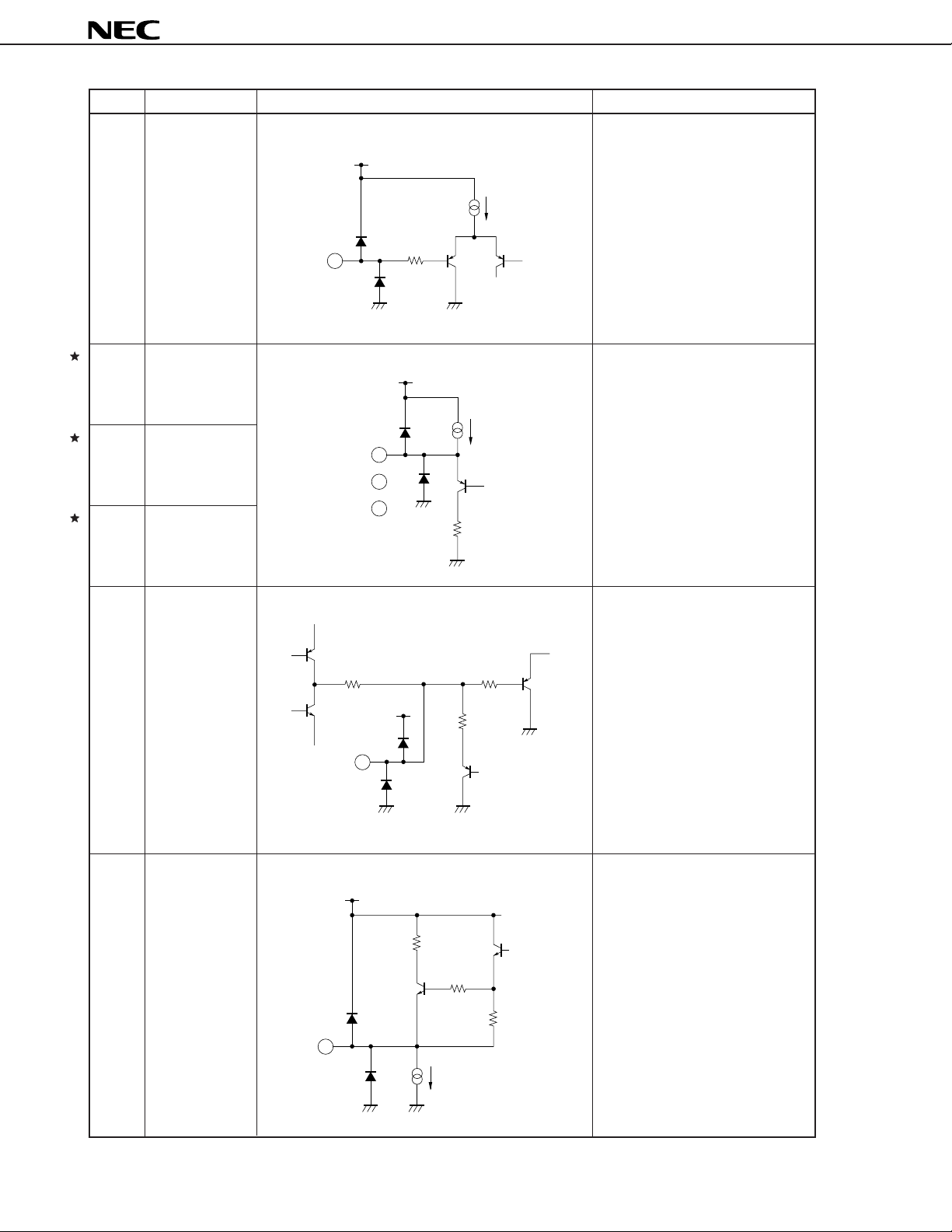
Y signal is output.
DC level is approx. 2.0 V.
CC
V
2 mA
12
13
14
50 Ω
Decoder R-Y and B-Y color
difference signal output pins.
DC level is approx. 2.5 V.
Video section ground.
µ
PC1830
Pin No. Pin name Equivalent circuit Function descriptions
16 Y input
17 Power supply
(video section)
18 R-Y input
19 B-Y input
V
CC
5 kΩ
16
V
CC
18
19
5 kΩ
5 kΩ
40 A
5 kΩ
40 A
µ
µ
Matrix Y signal input pin. This pin
also serves as a clamp pin. Input
the signal with C coupling. DC
level is approx. 2.0 V.
Video section power supply.
Matrix R-Y and B-Y color difference
signal input pins. These pins also
serve as clamp pins.
Input the signals with C coupling.
DC level is approx. 2.5 V.
Output in PAL mode is “pseud
PAL”.
20 Color control
21 Tint control
Pin for color adjustment of matrix
V
CC
10 kΩ
40 kΩ
70 kΩ
20
21
circuit.
Pin for tint adjustment of matrix
circuit.
7
Pin No. Pin name Equivalent circuit Function descriptions
22 Clamp pulse
input
V
CC
20 A
µ
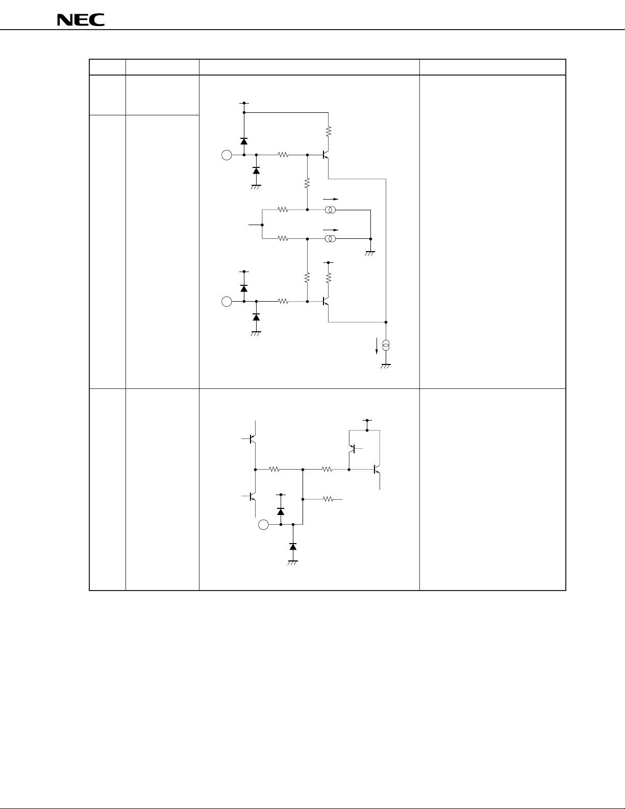
Matrix clamp pulse input pin.
Clamp operation is performed at
2.8 V or more.
µ
PC1830
23 R output
24 G output
25 B output
26 Color killer
filter
22
500 Ω
10 kΩ
Matrix R, G, and B output pins.
V
CC
2 mA
23
24
25
50 Ω
10 kΩ
DC level is approx. 2.0 V.
Sync. signal component, added to
Y-input (16 pin), appears in R, G,
and B output pins.
Filter connection pin of color killer
sync detector.
27 fSC VCO output
V
CC
10 kΩ
26
fSC VCO oscillator output pin.
VCC
125 Ω
125 Ω
3.3 kΩ
27
2.9 mA
Connect this pin to pin 28 via a
3.58 MHz oscillation filter and to
pin 29 via a 4.43 MHz oscillation
filter.
8
µ
PC1830
Pin No. Pin name Equivalent circuit Function descriptions
28 fSC VCO input
(3.58 MHz)
V
CC
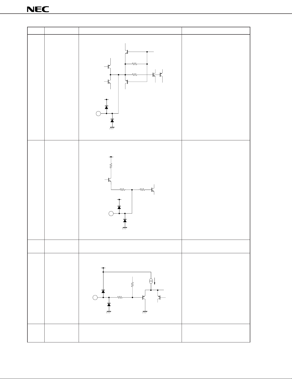
fSC VCO input pins. Connect a
3.58 MHz oscillation filter between
pins 27 and 28 and a 4.43 MHz
29 fSC VCO input
(4.43 MHz)
5 kΩ
5 kΩ
28
oscillation filter between pins 27
and 29. Switch of pin 28 input and
pin 29 input is suppressed in
response to pin 41 (fSC switch)
voltage.
10 kΩ
60/0 A
µ
20 kΩ
0/60 A
µ
20 kΩ
V
V
CC
CC
10 kΩ 5 kΩ
30 Chroma APC
filter
29
5 kΩ
80 A
µ
Pin for connecting filter of chroma
V
CC
APC detector.
500 Ω 5 kΩ
V
CC
50 kΩ
30
9
Pin No. Pin name Equivalent circuit Function descriptions
31 fO adjustment
filter
30 kΩ
500 Ω
V
CC
31
Pin for connecting filter of fO
automatic adjustment loop.
µ
PC1830
32 ACC filter
33 GND (chroma
section)
34 Separate
chroma input
VCC
VCC
500 Ω
1 kΩ 5 kΩ
VCC
32
30 kΩ
80 A
µ
Pin for connecting filter of ACC
detector.
Chroma section ground.
Separate chroma signal input pin.
This pin also serves as a separate
and composite switch input pin. If
the pin voltage is set to 3.7 V or
more, composite input mode is
entered.
35 Power supply
(chroma
section)
10
34
5 kΩ
Chroma section power supply.
µ
PC1830
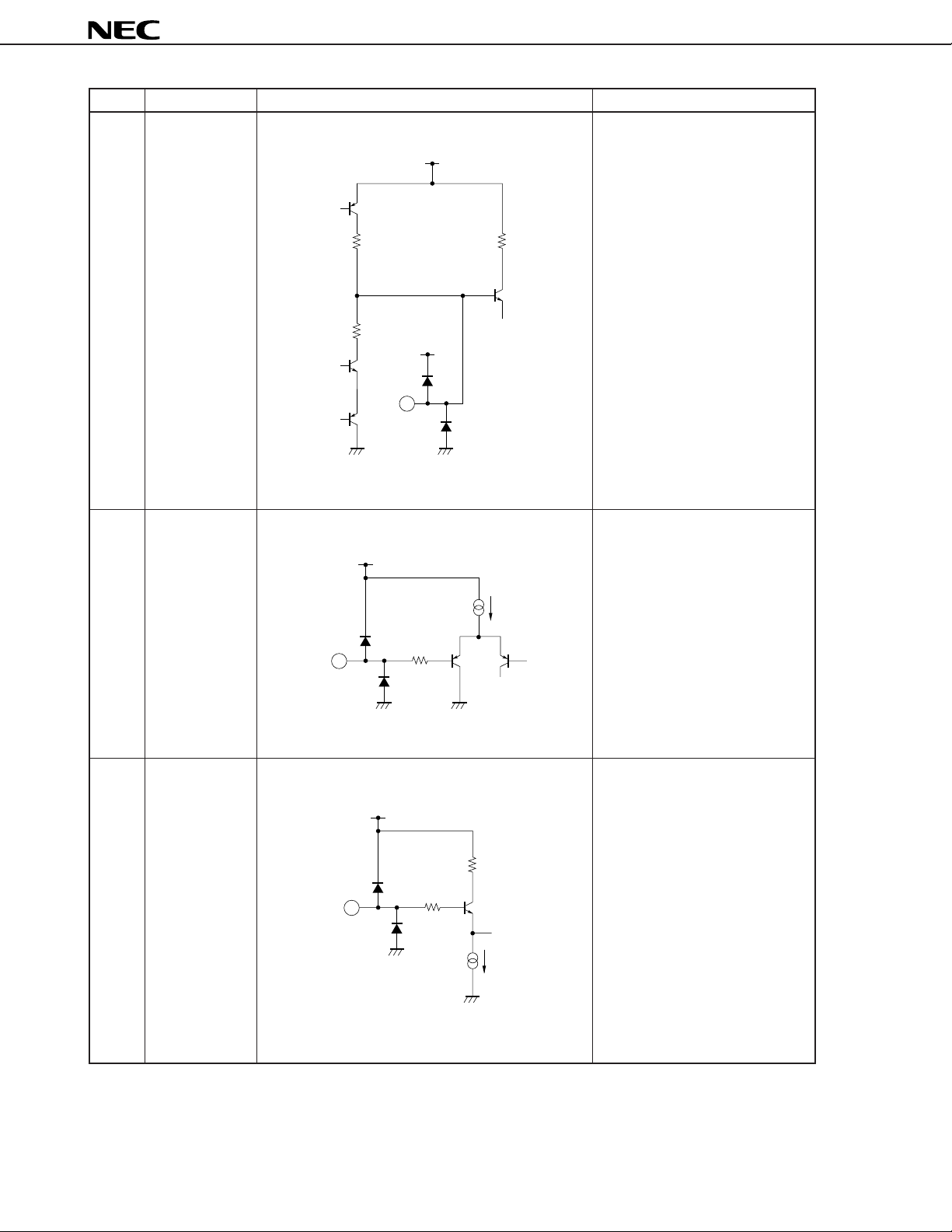
Pin No. Pin name Equivalent circuit Function descriptions
36 Composite
video signal
input
V
CC
5 kΩ
36
5 kΩ
Composite video signal or separate
Y signal input pin. This pin also
serves as a clamp pin.
Input the signal with C coupling.
DC level is approx. 2.3 V.
37 Subcolor
control
38 Contrast
control
39 Sync.
separation
input
Decoder color and contrast
V
CC
10 kΩ
40 kΩ
70 kΩ
37
38
V
CC
5 kΩ
adjustment pins.
Input pin of sync. separation
circuit.
5 kΩ
39
167 Ω
5 kΩ
V
CC
16 kΩ
100 Ω
11
Pin No. Pin name Equivalent circuit Function descriptions
40 H sync. detect
filter
V
CC
Pin for connecting filter of H sync.
detector.
µ
PC1830
41 fSC switch
1 kΩ
10 kΩ
41
10 kΩ
V
CC
40
Pin for controlling fSC VCO input
V
CC
20 A
µ
5 kΩ
(pins 28, 29) switch. When the pin
voltage is 2.8 V or more, the mode
changes to the 3.58 MHz mode;
when 2.2 V or less, to the 4.43
MHz mode.
42 NTSC/PAL
switch
12
Pin for controlling switch of NTSC
and PAL modes of decoder and
V
CC
5 kΩ
42
5 kΩ
20 A
µ
matrix. One of the following three
combinations of decoder and
matrix modes can be selected
depending on the value of the pin
42 voltage V42:
1. When V42 = 0 V
decoder = PAL
matrix = PAL
2. When V42 = 2.5 V
decoder = NTSC
matrix = NTSC
3. When V42 = 5 V
decoder = NTSC
matrix = PAL

µ
PC1830
5. BLOCK OPERATION
5.1 Video Signal Processing Section
(1) Input signal
After coupling by a capacitor (0.22 µF), a 1 Vp-p composite video signal is input to the composite video signal input
pin (pin 36).
(2) Clamp circuit
The clamp circuit controls the pedestal voltage level to be constant to make it a reference voltage for the post-stage
signal processing.
(3) Chroma trap circuit
Eliminates the chroma signal (NTSC system: approximately 3.58 MHz, PAL system: approximately 4.43 MHz) from
a composite video signal and extracts a brightness signal.
(4) Separate/composite switching circuit
Operates as shown in Table 5-1 according to the voltage of the separate chroma input pin (pin 34).
Table 5-1. Operation when Switching Separate/Composite Signals
Separate chroma input Mode Brightness signal ACC amp input
pin (pin 34) voltage processing
Less than 3.7 V Y/C separate input Without chroma trap Input from separate chroma
3.7 V or higher Composite video input With chroma trap Input from chroma BPF
(5) Delay circuit
Compensates for the delay between the brightness signal and chroma signal by delaying the brightness signal.
(6) Contrast adjustment circuit
Adjusts the amplitude of the brightness signal output from the Y output pin (pin 12) according to the voltage of the
contrast control pin (pin 38).
The control characteristic is shown in Figure 5-1.
13

µ
PC1830
Figure 5-1. Contrast Control Characteristic
(a) NTSC mode (b) PAL mode
400 mV
p-p
stair step (composite) input
2
V
CC
= 5 V
2
400 mV
p-p
stair step (composite) input
V
CC
= 5 V
)
p-p
1
Y output voltage (V
0 12345
Contrast control pin voltage (V)
5.2 Chroma Signal Processing Section
(1) Input signal
• Composite video signal input
After coupling by a capacitor (0.22 µF), a 1 Vp-p composite video signal is input to the composite video signal
input pin (pin 36).
• Separate chroma signal input
After coupling by a capacitor (1000 pF), a chroma signal whose burst signal amplitude is 150 mV
to the separate chroma input pin (pin 34).
)
p-p
1
Y output voltage (V
0 12345
Contrast control pin voltage (V)
p-p is input
(2) Chroma BPF circuit
Separates the chroma signal from a composite video signal.
(3) Separate/composite switching circuit
When the potential of the separate chroma input pin (pin 34) is 3.7 V or higher (in composite mode), switches the ACC
amp input from the chroma input pin to the chroma BPF circuit output. Processing of the brightness signal at this time
is switched so that it passes through the chroma trap circuit.
Operation when switching separate/composite signals is shown in Table 5-1.
(4) ACC (Auto Color Control) amplification circuit
Extracts the burst signal, detects its level and smoothes the voltage of the ACC filter pin (pin 32) by an external
capacitor.
This smoothed voltage controls color gain to keep the amplitude of the burst signal constant.
14
 Loading...