NEC UPC1676P, UPC1676G, UPC1676B Datasheet

DATA SHEET
BIPOLAR ANALOG INTEGRATED CIRCUIT
µµµµ
PC1676G
GENERAL PURPOSE WIDE BNAD AMPLIFIER
DESCRIPTION
The µPC1676G is a silicon monolithic integrated circuit employing small package (4pins mini mold) and designed
for use as a wide band amplifier covers from HF band to UHF band.
FEATURES
• Excellent frequency response : 1.2 GHz TYP.
@ 3 dB down below flat gain.
• High power gain : 22 dB TYP. @ f = 0.5 GHz.
• High isolation.
• Super small package.
• Uni- and low voltage operation : VCC = 5 V
• Input and output matching 50 Ω.
ABSOLUTE MAXIMUM RATINGS (TA = 25
Supply Voltage V
Total Power Dissipation P
Operating Temperature T
Storage Temperature T
CC
T
opt
stg
ELECTRICAL CHARACTERISTICS (TA = 25
CHARACTERISTIC SYMBOL MIN. TYP. MAX. UNIT TEST CONDITIONS
Circuit Current I
Power Gain G
Noise Figure NF 4.5 6.0 dB f = 0.5 GHz
Upper Limit Operating Frequency f
Isolation ISL 24 28 dB f = 0.5 GHz
Input Return Loss RL
Output Return Loss RL
Maximum Output Level P
NEC cannot assume any responsibility for any circuits shown or represent that
they are free from patent infringement.
CC
P
u
in
out
O
C)
°°°°
6V
200 mW
40 to +85°C
−
55 to +150°C
−
C, VCC = 5 V)
°°°°
14 19 24 mA No Signal
19 22 24 dB f = 0.5 GHz
1.0 1.2 GHz 3 dB down below flat gain
9 12 dB f = 0.5 GHz
6 9 dB f = 0.5 GHz
3 5 dBm f = 0.5 GHz, Pin = 0 dBm
Document No. P12447EJ2V0DS00 (2nd edition)
(Previous No. IC-1891)
Date Published March 1997 N
Printed in Japan
1989©

µµµµ
PC1676G
TYPICAL CHARACTERISTICS (TA = 25
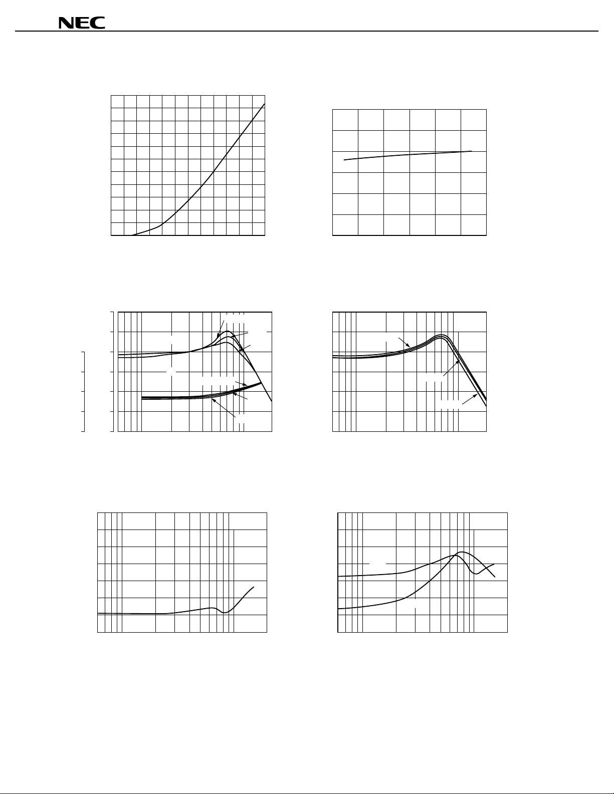
CIRCUIT CURRENT vs. SUPPLY VOLTAGE
25
20
15
10
-Circuit Current-mA
CC
I
5
1234560
CC
-Supply Voltage-V
V
NOISE FIGURE AND INSERTION POWER
GAIN vs. FREQUENCY
10
30
20
G
P
VCC = 5.5 V
°°°°
C)
5.0 V
4.5 V
CIRCUIT CURRENT vs. OPERATING
TEMPERATURE
30
20
-Circuit Current-mA
10
CC
I
0
−50 0 50 100
opt
-Operating Temperature-°C
T
INSERTION POWER GAIN vs. FREQUENCY
30
TA = −40 °C
20
VCC = 5 V
5
10
-Insertion Power Gain-dB
P
G
NF-Noise Figure-dB
0
0
60 100 200 500 1000 2000
REVERSE INSERTION GAIN vs. FREQUENCY
0
−10
−20
ISL-Isolation-dB
−30
100
60
NF
VCC = 5.5 V
5.0 V
4.5 V
f-Frequency-MHz
VCC = 5 V VCC = 5 V
200 500 1000 2000
f-Frequency-MHz
+25 °C
10
-Insertion Power Gain-dB
P
G
0
60 100 200 500 1000 2000
+85 °C
f-Frequency-MHz
INPUT AND OUTPUT RETURN LOSS vs.
FREQUENCY
0
−10
-Output Return Loss-dB
−20
-Input Return Loss-dB
in
out
RL
RL
−30
60
100
RL
out
RL
in
200 500 1000 2000
f-Frequency-MHz
2

µµµµ
PC1676G
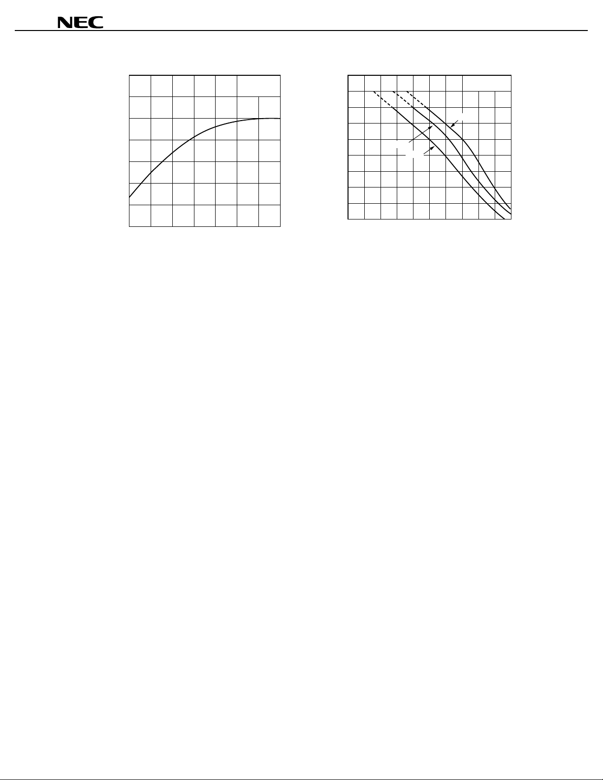
OUTPUT POWER vs. INPUT POWER
10
0
-Output Power-dBm
o
−10
P
−20
P
in
-Input Power-dBm
S-PARAMETER
VCC = 5 V, ZO = 50
f (MHz) S11∠ S
100
200
400
600
800
1000
1200
1400
1600
0.072
0.093
0.175
0.355
0.485
0.387
0.298
0.243
0.208
−20 −10 0−30
−26.5
−63.5
−120.4
−176.4
118.7
77.5
59.2
50.5
47.1
11
VCC = 5 V
f = 500 MHz
S21∠ S
8.955
9.327
11.021
14.504
14.530
9.478
6.301
4.562
3.506
THIRD ORDER INTERMODULATION DISTORTION
vs. OUTPUT POWER OF EACH TONE
−50
−40
5.0 V
−30
−20
-3rd Order Intermodulation Distortion-dBc
3
−10
IM
out
-Output Power of Each Tone-dBm
P
21
−15.3
−31.3
−66.2
−114.3
177.1
123.1
85.6
53.8
24.5
S12∠ S
0.034
0.035
0.038
0.042
0.037
0.044
0.057
0.070
0.083
4.5 V
−2.0
−3.4
−8.4
−18.4
−25.7
−20.5
−28.3
−41.5
−56.4
1
= 500 MHz
f
f2 = 504 MHz
5.5 V
0−20 −10
12
S22∠ S
0.220
0.233
0.303
0.408
0.361
0.231
0.251
0.292
0.313
22
171.2
161.3
139.4
107.7
65.5
61.6
68.0
61.9
51.5
3
 Loading...