

NEC UPA1456H Datasheet
(E)
DATA SHEET
SILICON TRANSISTOR ARRAY
µ
PA1456
NPN SILICON POWER TRANSISTOR ARRAY
LOW SPEED SWITCHING USE (DARLINGTON TRANSISTOR)
INDUSTRIAL USE
DESCRIPTION
The µPA1456 is NPN silicon epitaxial Darlington
Power Transistor Array that built in 4 circuits designed
for driving solenoid, relay, lamp and so on.
FEATURES
• Easy mount by 0.1 inch of terminal interval.
• High hFE for Darlington Transistor.
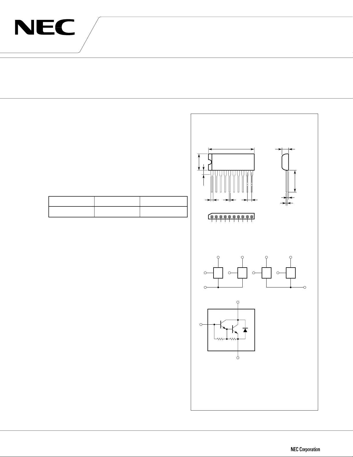
ORDERING INFORMATION
Part Number Package Quality Grade
µ
PA1456H 10 Pin SIP Standard
Please refer to "Quality grade on NEC Semiconductor Devices"
(Document number IEI-1209) published by NEC Corporation to
know the specification of quality grade on the devices and its
recommended applications.
ABSOLUTE MAXIMUM RATINGS (Ta = 25 ˚C)
Collector to Base Voltage VCBO 150 V
Collector to Emitter Voltage V
Emitter to Base Voltage V
Collector Current (DC) I
Collector Current (pulse) I
Base Current (DC) I
Total Power Dissipation P
Total Power Dissipation P
Junction Temperature T
Storage Temperature T
* PW ≤ 300 µs, Duty Cycle ≤ 10 %
** 4 Circuits, T
*** 4 Circuits, T
a = 25 ˚C
c = 25 ˚C
CEO 100 V
EBO 7V
C(DC) ±5 A/unit
C(pulse)* ±10 A/unit
B(DC) 0.5 A/unit
T1** 3.5 W
T2*** 28 W
j 150 ˚C
stg –55 to +150 ˚C
26.8 MAX.
10
2.5
1.4 0.6 ±0.1
1 2 3 4 5 6 7 8 9 10
3
2
1
(B)
1 R2
R
PACKAGE DIMENSION
(in millimeters)
4.0
2.54
CONNECTION DIAGRAM
579
468
(C)
PIN No.
2, 4, 6, 8
3, 5, 7, 9
1, 10
R
R
: Base (B)
: Collector (C)
: Emitter (E)
.
1 = 3.0 kΩ
.
.
2 = 300 Ω
.
MIN.
1.4
0.5 ±0.1
10
Document No. IC-3521
(O. D. No. IC-6340)
Date Published September 1994 P
Printed in Japan
The information in this document is subject to change without notice.
©
1994
ELECTRICAL CHARACTERISTICS (Ta = 25 ˚C)
y Cy
CHARACTERISTIC SYMBOL MIN. TYP. MAX. UNIT TEST CONDITIONS
Collector Leakage Current ICBO 10
Emitter Leakage Current IEBO 10 mA VEB = 5 V, IC = 0
DC Current Gain hFE1
DC Current Gain hFE2
Collector Saturation Voltage VCE(sat)
Base Saturation Voltage VBE(sat)
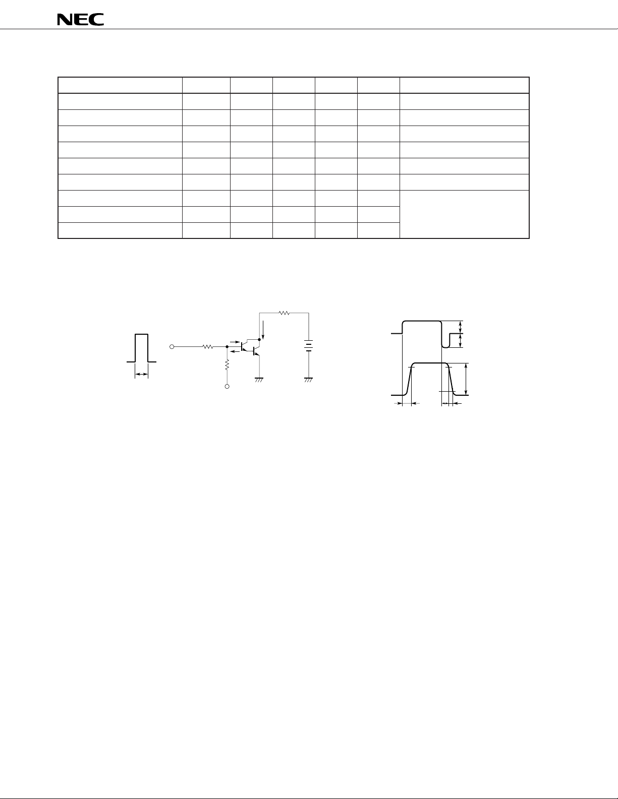
Turn On Time ton 1
Storage Time tstg 3
Fall Time tf 1
*
2000 7000 20000 — VCE = 2 V, IC = 2 A
*
500 3000 — VCE = 2 V, IC = 4 A
*
*
0.9 1.5 V IC = 2 A, IB = 2 mA
1.6 2 V IC = 2 A, IB = 2 mA
µ
A VCB = 100 V, IE = 0
µ
s
IC = 2 A
µ
µ
IB1 = –IB2 = 2 mA
s
s
.
VCC = 50 V, RL = 25 Ω
.
See test circuit
* PW ≤ 350 µs, Duty Cycle ≤ 2 % / pulsed
SWITCHING TIME TEST CIRCUIT
L = 25 Ω
R
.
V
CC = 50 V
.
Base Current
Wave Form
Collector
Current
Wave Form
90 %
10 %
ton tstg tf
VIN
PW
.
.
µ
cle ≤ 2 %
PW = 50 s
Dut
B1
I
IB2
.
VBB = –5 V
.
IC
T.U.T.
.
.
I
IB2
µ
PA1456
B1
IC
2
 Loading...