

Page 1

USER'S MANUAL
µPD750008
4 BIT SINGLE-CHIP MICROCOMPUTER
µPD750004
µPD750006
µPD750008
µPD75P0016
Document No. U10740EJ2V0UM00 (2nd edition)
(Previous No. IEU-1421)
Date Published April 1996 P
©
1995
Printed in Japan
Page 2

GENERAL
1
PIN FUNCTIONS
FEATURES OF THE ARCHITECTURE AND MEMORY MAP
INTERNAL CPU FUNCTIONS
PERIPHERAL HARDWARE FUNCTIONS
INTERRUPT AND TEST FUNCTIONS
STANDBY FUNCTION
RESET FUNCTION
WRITING TO AND VERIFYING PROGRAM MEMORY (PROM)
MASK OPTION
INSTRUCTION SET
FUNCTIONS OF THE µPD75008, µPD750008, AND µPD75P0016
DEVELOPMENT TOOLS
MASK ROM ORDERING PROCEDURE
2
3
4
5
6
7
8
9
10
11
A
B
C
INSTRUCTION INDEX
HARDWARE INDEX
RIVISION HISTORY
D
E
F
Page 3

The export of this product from Japan is regulated by the Japanese government. To export this product may be prohibited
without governmental license, the need for which must be judged by the customer. The export or re-export of this product
from a country other than Japan may also be prohibited without a license from that country. Please call an NEC sales
representative.
The information in this document is subject to change without notice.
No part of this document may be copied or reproduced in any form or by any means without the prior written
consent of NEC Corporation. NEC Corporation assumes no responsibility for any errors which may appear in
this document.
NEC Corporation does not assume any liability for infringement of patents, copyrights or other intellectual property
rights of third parties by or arising from use of a device described herein or any other liability arising from use
of such device. No license, either express, implied or otherwise, is granted under any patents, copyrights or other
intellectual property rights of NEC Corporation or others.
While NEC Corporation has been making continuous effort to enhance the reliability of its semiconductor devices,
the possibility of defects cannot be eliminated entirely. To minimize risks of damage or injury to persons or
property arising from a defect in an NEC semiconductor device, customer must incorporate sufficient safety
measures in its design, such as redundancy, fire-containment, and anti-failure features.
NEC devices are classified into the following three quality grades:
“Standard“, “Special“, and “Specific“. The Specific quality grade applies only to devices developed based on a
customer designated “quality assurance program“ for a specific application. The recommended applications of
a device depend on its quality grade, as indicated below. Customers must check the quality grade of each device
before using it in a particular application.
Standard:Computers, office equipment, communications equipment, test and measurement equipment, audio
and visual equipment, home electronic appliances, machine tools, personal electronic equipment
and industrial robots
Special: Transportation equipment (automobiles, trains, ships, etc.), traffic control systems, anti-disaster
systems, anti-crime systems, safety equipment and medical equipment (not specifically designed
for life support)
Specific: Aircrafts, aerospace equipment, submersible repeaters, nuclear reactor control systems, life
support systems or medical equipment for life support, etc.
The quality grade of NEC devices in “Standard“ unless otherwise specified in NEC's Data Sheets or Data Books.
If customers intend to use NEC devices for applications other than those specified for Standard quality grade,
they should contact NEC Sales Representative in advance.
Anti-radioactive design is not implemented in this product.
M7 94.11
Page 4

Major Changes
Page Description
All The 44-pin plastic QFP package has been changed from µPD750008GB-xxx-3B4
to µPD750008GB-xxx-3BS-MTX.
The µPD75P0016 under development has been changed to the already-developed
µPD75P0016.
The input withstand voltage at ports 4 and 5 during open drain has been changed from
12 V to 13 V.
Preface English-version document numbers have been added to "Related documents."
p.4 The format of the table in Section 1.3 has been changed.
p.45 The caution in using Mk II mode has been added in Section 4.1.1 .
p.85 The description for the mask option when using the feedback resistor has been added in
(6) in Section 5.2.2.
p.187 The description for the interrupt enable flag has been added in Section 6.3.
p.198 Table 6-4 has been added in Section 6.6.
p.233 Section 9.4 has been added.
p.235 Chapter 10 has been added.
p.237–298 The operand @rpa has been changed to @rpa1 in Section 11.
p.241 @rpa1 has been added in the table in (1) in Section 11.2.
p.264 The title of Section 11.4 has been modified to conform to that of Section 11.2.
p.301 Appendix B
Supported OS versions have been upgraded.
p.321 Appendix F has been added.
The mark * shows major revised points.
Page 5

PREFACE
Readers This manual is intended for engineers who want to learn the capabilities of the
µPD750004, µPD750006, µPD750008, and µPD75P0016 to develop application systems
based on them.
Purpose The purpose of this manual is to help users understand the hardware capabilities (shown
below) of the µPD750004, µPD750006, µPD750008, and µPD75P0016.
Configuration This manual is roughly divided as follows:
• General
• Pin functions
• Architecture feature and memory map
• Internal CPU functions
• Peripheral hardware functions
• Interrupt and test functions
• Standby function
• Reset function
• Writing to and verifying program memory (PROM)
• Mask option
• Instruction set
Guidance Readers of this manual should have general knowledge of the electronics, logical circuit,
and microcomputer fields.
• For users who have used the µPD75008:
–> See Appendix A to check for any difference in the functions and read the
explanation of those differences.
• To check the functions of an instruction in detail when the reader knows its
mnemonics:
–> See the instruction index in Appendix D.
• To check the functions of specific internal circuits, etc.:
–> See Appendix E.
• To understand the overall functions of the µPD750004, µPD750006, µPD750008,
and µPD75P0016:
–> Read through all chapters sequentially.
Page 6

Notation Data bit significance : Higher-order bits on the left side
Lower-order bits on the right side
Active low : xxx (Pin and signal names are overscored.)
Memory map address : Low-order address on the upper side
High-order address on the lower side
Note : Explanation of an indicated part of text
Caution : Information requesting the user's special attention
Remark : Supplementary information
Important and emphasized matter : Described in bold face
Numeric value : Binary .................. xxxx or xxxxB
Decimal ............... xx xx
Hexadecimal ....... xxxxH
Page 7
Related documents Some documents are preliminary editions, but they are not so specified in the tables
below.
Documents related to devices
*
Document Name
µPD750004, 750006, 750008 Data Sheet U10738J IC-3647
µPD75P0016 Data Sheet U10328J To be prepared
µPD750008 User’s Manual U10740J (This manual) IEU-1421
µPD750008 Instruction List IEM-5593 —
75XL Series Selection Guide U10453J U10453E
Document Number
Japanese English
Documents related to development tools
Document Name
Hardware IE-75000-R/IE-75001-R User’s Manual EEU-846 EEU-1416
IE-75300-R-EM User’s Manual EEU-951 EEU-1493
EP-75008CU-R User’s Manual EEU-699 EEU-1317
EP-75008GB-R User's Manual EEU-698 EEU-1305
PG-1500 User’s Manual EEU-651 EEU-1335
Software RA75X Assembler Package User’s Operation EEU-731 EEU-1346
Manual
PG-1500 Controller PC-9800 Series (MS-DOSTM) Base EEU-704 EEU-1291
User’s Manual
IBM PC Series (PC DOS
Language EEU-730 EEU-1363
TM
) Base EEU-5008 U10540E
Document Number
Japanese English
Other documents
Document Name
Package Manual IEI-635 IEI-1213
Semiconductor Device Mounting Technology Manual IEI-616 IEI-1207
Quality Grade on NEC Semiconductor Devices IEI-620 IEI-1209
Reliability and Quality Control of NEC Semiconductor Devices IEI-5068 —
Electrostatic Discharge (ESD) Test MEM-539 —
Semiconductor Device Quality Guarantee Guide MEI-603 MEI-1202
Microcontroller-Related Products Guide - by third parties MEI-604 —
Document Number
Japanese English
Caution The above related documents are subject to change without notice. Be sure to use the
latest edition when you design your system.
Page 8

[MEMO]
Page 9

CONTENTS
CHAPTER 1 GENERAL ......................................................................................................................... 1
1.1 FUNCTION OVERVIEW ......................................................................................... 2
1.2 ORDERING INFORMATION................................................................................... 3
1.3 DIFFERENCES AMONG SUBSERIES PRODUCTS ............................................. 4
1.4 BLOCK DIAGRAM .................................................................................................. 5
1.5 PIN CONFIGURATION (TOP VIEW) ..................................................................... 6
CHAPTER 2 PIN FUNCTIONS .............................................................................................................. 9
2.1 PIN FUNCTIONS OF THE µPD750008 ................................................................. 9
2.2 PIN FUNCTIONS .................................................................................................... 12
2.2.1 P00-P03 (PORT0)...................................................................................... 12
P10-P13 (PORT1)...................................................................................... 12
2.2.2 P20-P23 (PORT2)...................................................................................... 13
P30-P33 (PORT3)...................................................................................... 13
P40-P43 (PORT4), P50-P53 (PORT5) ..................................................... 13
P60-P63 (PORT6), P70-P73 (PORT7) ..................................................... 13
2.2.3 P80, P81 (PORT8)..................................................................................... 13
2.2.4 TI0 .............................................................................................................. 13
2.2.5 PTO0, PTO1 .............................................................................................. 13
2.2.6 PCL............................................................................................................. 14
2.2.7 BUZ ............................................................................................................ 14
2.2.8 SCK, SO/SB0, SI/SB1 ............................................................................... 1 4
2.2.9 INT4............................................................................................................ 14
2.2.10 INT0, INT1 ................................................................................................ 14
2.2.11 INT2 .......................................................................................................... 1 5
2.2.12 KR0-KR3................................................................................................... 15
KR4-KR7................................................................................................... 15
2.2.13 X1, X2 ....................................................................................................... 15
2.2.14 XT1, XT2................................................................................................... 16
2.2.15 RESET ...................................................................................................... 16
2.2.16 V
2.2.17 V
......................................................................................................................................... 16
DD
......................................................................................................................................... 16
SS
2.2.18 IC (for the µPD750004, µPD750006, and µPD750008 only).................. 17
2.2.19 VPP (for the µPD75P0016 only)............................................................... 1 7
2.2.20 MD0-MD3 (for the µPD75P0016 only)..................................................... 17
2.3 PIN INPUT/OUTPUT CIRCUITS ............................................................................ 18
2.4 CONNECTION OF UNUSED PINS........................................................................ 20
- i -
Page 10

CHAPTER 3 FEATURES OF THE ARCHITECTURE AND MEMORY MAP ....................................... 21
3.1 DATA MEMORY BANK STRUCTURE AND ADDRESSING MODES .................. 21
3.1.1 Data Memory Bank Structure .................................................................... 21
3.1.2 Data Memory Addressing Modes .............................................................. 23
3.2 GENERAL REGISTER BANK CONFIGURATION ................................................. 3 4
3.3 MEMORY -M APP ED I /O .......................................................................................... 39
CHAPTER 4 INTERNAL CPU FUNCTIONS ......................................................................................... 45
4.1 Mk I MODE/Mk II MODE SWITCH FUNCTIONS................................................... 45
4.1.1 Differences between Mk I Mode and Mk II Mode..................................... 45
4.1.2 Setting of the Stack Bank Selection Register (SBS)................................ 46
4.2 PROGRAM COUNTER (PC) ................................................................................. 47
4.3 PROGRAM MEMORY (ROM) ................................................................................ 48
4.4 DATA MEMORY (RAM) .......................................................................................... 5 3
4.4.1 Data Memory Configuration....................................................................... 5 3
4.4.2 Specification of a Data Memory Bank....................................................... 54
4.5 GENERAL REGISTER............................................................................................ 56
4.6 ACCUMULATOR..................................................................................................... 5 7
4.7 STACK POINTER (SP) AND STACK BANK SELECT REGISTER (SBS)............ 58
4.8 PROGRAM STATUS WORD (PSW) ...................................................................... 62
4.9 BANK SELECT REGISTER (BS) ........................................................................... 65
CHAPTER 5 PERIPHERAL HARDWARE FUNCTIONS ...................................................................... 6 7
5.1 DIGITAL I/O PORTS............................................................................................. 67
5.1.1 Types, Features, and Configurations of Digital I/O Ports ........................ 68
5.1.2 I/O Mode Setting........................................................................................ 74
5.1.3 Digital I/O Port Manipulation Instructions ................................................. 76
5.1.4 Digital I/O Port Operation .......................................................................... 7 9
5.1.5 Specification of Bilt-in Pull-Up Resistors .................................................. 81
5.1.6 I/O Timing of Digital I/O Ports ................................................................... 82
5.2 CLOCK GENERA TOR ............................................................................................ 8 4
5.2.1 Clock Generator Configuration.................................................................. 84
5.2.2 Functions and Operations of the Clock Generator ................................... 85
5.2.3 System Clock and CPU Clock Setting ...................................................... 94
5.2.4 Clock Output Circuit................................................................................... 96
5.3 BASIC INTERVAL TIMER/WATCHDOG TIMER ................................................... 99
5.3.1 Configuration of the Basic Interval Timer/Watchdog Timer ..................... 99
5.3.2 Basic Interval Timer Mode Register (BTM) .............................................. 99
5.3.3 Watchdog Timer Enable Flag (WDTM)..................................................... 101
5.3.4 Operation of the Basic Interval Timer ....................................................... 10 1
- ii -
Page 11

5.3.5 Operation of the Watchdog Timer ............................................................. 102
5.3.6 Other Functions ......................................................................................... 103
5.4 CLOCK TIMER ........................................................................................................ 105
5.4.1 Configuration of the Clock Timer .............................................................. 106
5.4.2 Clock Mode Register ................................................................................. 106
5.5 TIMER/EVENT COUNTER ..................................................................................... 108
5.5.1 Configuration of Timer/Event Counter ...................................................... 108
5.5.2 8-Bit Timer/Event Counter Mode Operation ............................................. 114
5.5.3 Notes on Timer/Event Counter Applications............................................. 120
5.6 SERIAL INTERFACE.............................................................................................. 1 23
5.6.1 Serial Interface Functions.......................................................................... 123
5.6.2 Configuration of Serial Interface ............................................................... 124
5.6.3 Register Functions ..................................................................................... 127
5.6.4 Operation Halt Mode.................................................................................. 13 5
5.6.5 Three-Wire Serial I/O Mode Operations ................................................... 137
5.6.6 Two-Wire Serial I/O Mode ......................................................................... 144
5.6.7 SBI Mode Operation .................................................................................. 150
5.6.8 Manipulation of SCK Pin Output ............................................................... 179
5.7 BIT SEQUENTIAL BUFFER ................................................................................... 181
CHAPTER 6 INTERRUPT AND TEST FUNCTIONS .............................................................................. 183
6.1 CONFIGURATION OF THE INTERRUPT CONTROL CIRCUIT........................... 183
6.2 TYPES OF INTERRUPT SOURCES AND VECTOR TABLES ............................. 185
6.3 VARIOUS DEVICES TO CONTROL INTERRUPT FUNCTIONS.......................... 1 87
6.4 INTERRUPT SEQUENCE ...................................................................................... 195
6.5 MULTIPLE INTERRUPT PROCESSING CONTROL............................................. 1 96
6.6 PROCESSING OF INTERRUPTS SHARING A VECTOR ADDRESS ................. 198
6.7 MACHINE CYCLES FOR STARTING INTERRUPT PROCESSING .................... 200
6.8 EFFECTIVE USE OF INTERRUPTS ..................................................................... 202
6.9 INTERRUPT APPLICATIONS ................................................................................ 202
6.10 TEST FUNCTION ................................................................................................. 210
6.10.1 Test Sources.......................................................................................... 21 0
6.10.2 Hardware to Control Test Functions ..................................................... 210
CHAPTER 7 STANDBY FUNCTION ..................................................................................................... 215
7.1 SETTING OF STANDBY MODES AND OPERATION STATUS ........................... 216
7.2 RELEASE OF THE STANDBY MODES................................................................. 2 17
7.3 OPERATION AFTER A STANDBY MODE IS RELEASED ................................... 219
7.4 SELECTION OF A MASK OPTION ........................................................................ 220
7.5 APPLICATIONS OF THE STANDBY MODES....................................................... 22 0
- iii -
Page 12

CHAPTER 8 RESET FUNCTION ........................................................................................................... 225
CHAPTER 9 WRITING TO AND VERIFYING PROGRAM MEMORY (PROM) ................................... 229
9.1 OPERATING MODES WHEN WRITING TO AND VERIFYING
THE PROGRAM MEMORY .................................................................................... 230
9.2 WRITING TO THE PROGRAM MEMORY ............................................................. 230
9.3 READING THE PROGRAM MEMORY .................................................................. 232
*
9.4 SCREENING OF ONE-TIME PROM ...................................................................... 233
CHAPTER 10 MASK OPTION ............................................................................................................... 235
*
10.1 PIN......................................................................................................................... 235
10.2 MASK OPTION OF STANDBY FUNCTION......................................................... 2 35
10.3 MASK OPTION FOR FEEDBACK RESISTOR OF SUBSYSTEM CLOCK ........ 236
CHAPTER 11 INSTRUCTION SET .......................................................................................................... 2 37
11.1 UNIQUE INSTRUCTIONS .................................................................................... 23 7
11.1.1 GETI Instruction ..................................................................................... 237
11.1.2 Bit Manipulation Instructions .................................................................. 238
11.1.3 String-Effect Instructions........................................................................ 2 38
11.1.4 Number System Conversion Instructions .............................................. 23 9
11.1.5 Skip Instructions and the Number of Machine Cycles Required
for a Skip ............................................................................................... 240
11.2 INSTRUCTION SET AND OPERATION .............................................................. 241
11.3 INSTRUCTION CODES OF EACH INSTRUCTION ............................................ 258
11.4 FUNCTIONS AND APPLICATIONS OF THE INSTRUCTIONS.......................... 26 4
11.4.1 Transfer Instructions .............................................................................. 264
11.4.2 Table Reference Instructions................................................................. 2 7 0
11.4.3 Bit Transfer Instructions ......................................................................... 273
11.4.4 Arithmetic/Logical Instructions ............................................................... 273
11.4.5 Accumulator Manipulation Instructions.................................................. 279
11.4.6 Increment/Decrement Instructions......................................................... 2 79
11.4.7 Compare Instructions ............................................................................. 280
11.4.8 Carry Flag Manipulation Instructions..................................................... 2 8 1
11.4.9 Memory Bit Manipulation Instructions ................................................... 282
11.4.10 Branch Instructions .............................................................................. 28 4
11.4.11 Subroutine Stack Control Instructions ................................................. 289
11.4.12 Interrupt Control Instructions ............................................................... 293
11.4.13 I/O Instructions ..................................................................................... 29 4
11.4.14 CPU Control Instructions ..................................................................... 295
11.4.15 Special Instructions .............................................................................. 295
- iv -
Page 13

APPENDIX A FUNCTIONS OF THE µPD75008, µPD750008, AND µPD75P0016 ............................ 2 99
APPENDIX B DEVELOPMENT TOOLS................................................................................................ 30 1
APPENDIX C MASKED ROM ORDERING PROCEDURE ................................................................... 3 09
APPENDIX D INSTRUCTION INDEX.................................................................................................... 31 1
D.1 INSTRUCTION INDEX (BY FUNCTION) .............................................................. 311
D.2 INSTRUCTION INDEX (ALPHABETICAL ORDER) ............................................. 314
APPENDIX E HARDWARE INDEX.......................................................................................................... 317
E.1 HARDWARE INDEX (ALPHABETICAL ORDER WITH RESPECT TO THE.......
HARDWARE NAME).............................................................................................. 317
E.2 HARDWARE INDEX (ALPHABETICAL ORDER WITH RESPECT TO THE
HARDWARE SYMBOL) ......................................................................................... 319
APPENDIX F REVISION HISTORY ......................................................................................................... 321
*
- v -
Page 14

LIST OF FIGURES (1/4)
Figure No. Title Page
2-1 Pin Input/Output Circuits .................................................................................................. 18
3-1 Use of MBE = 0 Mode and MBE = 1 Mode..................................................................... 22
3-2 Data Memory Organization and Addressing Range of Each Addressing Mode ............ 24
3-3 Updating Static RAM Addresses ...................................................................................... 2 8
3-4 Example of Register Bank Selection ............................................................................... 35
3-5 General Register Configuration (4-bit Processing) ......................................................... 37
3-6 General Register Configuration (8-bit Processing) ......................................................... 38
3-7 µPD750008 I/O Map......................................................................................................... 40
4-1 Stack Bank Selection Register Format............................................................................ 46
4-2 Program Counter Organization ........................................................................................ 47
4-3 Program Memory Map (in µPD750004)........................................................................... 49
4-4 Program Memory Map (in µPD750006)........................................................................... 50
4-5 Program Memory Map (in µPD750008)........................................................................... 51
4-6 Program Memory Map (in µPD75P0016)......................................................................... 52
4-7 Data Memory Map ............................................................................................................ 5 4
4-8 General Register Format.................................................................................................. 56
4-9 Register Pair Format ........................................................................................................ 5 7
4-10 Accumulator ...................................................................................................................... 57
4-11 Format of Stack Pointer and Stack Bank Select Register .............................................. 59
4-12 Data Saved to the Stack Memory (Mk I Mode) ............................................................... 59
4-13 Data Restored from the Stack Memory (Mk I Mode) ...................................................... 60
4-14 Data Saved to the Stack Memory (Mk II Mode) .............................................................. 60
4-15 Data Restored from the Stack Memory (Mk II Mode) ..................................................... 61
4-16 Program Status Word Format .......................................................................................... 62
4-17 Bank Select Register Format ........................................................................................... 65
5-1 Data Memory Addresses of Digital Ports......................................................................... 6 7
5-2 Configurations of Ports 0 and 1 ....................................................................................... 69
5-3 Configurations of Ports 2 and 7 ....................................................................................... 70
5-4 Configurations of Ports 3n and 6n (n = 0 to 3) ................................................................ 71
5-5 Configurations of Ports 4 and 5 ....................................................................................... 72
5-6 Configuration of Port 8 ..................................................................................................... 73
5-7 Formats of Port Mode Registers...................................................................................... 75
5-8 Pull-Up Resistor Specification Register Format.............................................................. 82
- vi -
Page 15

LIST OF FIGURES (2/4)
Figure No. Title Page
5-9 I/O Timing Chart of Digital I/O Ports................................................................................ 82
5-10 ON Timing Chart of Built-in Pull-Up Resistor Connected by Software.......................... 8 3
5-11 Block Diagram of the Clock Generator ............................................................................ 84
5-12 Format of the Processor Clock Control Register............................................................. 8 7
5-13 Format of the System Clock Control Register ................................................................. 88
5-14 External Circuit for the Main System Clock Oscillator .................................................... 89
5-15 External Circuit for the Subsystem Clock Oscillator........................................................ 8 9
5-16 Examples of Oscillator Connections Which Should Be Avoided .................................... 90
5-17 Subsystem Clock Oscillator .............................................................................................. 9 2
5-18 Sub-Oscillator Control Register (SOS) Format ............................................................... 93
5-19 Changing the System Clock and CPU Clock ................................................................... 95
5-20 Configuration of the Clock Output Circuit ........................................................................ 96
5-21 Format of the Clock Output Mode Register..................................................................... 9 7
5-22 Application to Remote Control Output ............................................................................. 98
5-23 Block Diagram of the Basic Interval Timer/Watchdog Timer .......................................... 99
5-24 Format of the Basic Interval Timer Mode Register ......................................................... 100
5-25 Format of the Watchdog Timer Enable Flag (WDTM) ..................................................... 1 0 1
5-26 Block Diagram of the Clock Timer ................................................................................... 10 6
5-27 Clock Mode Register Format ........................................................................................... 107
5-28 Block Diagram of the Timer/Event Counter (Channel 0) ................................................ 109
5-29 Block Diagram of the Timer Counter (Channel 1)........................................................... 1 10
5-30 Timer/Event Counter Mode Register (Channel 0) Format .............................................. 112
5-31 Timer Counter Mode Register (Channel 1) Format......................................................... 11 3
5-32 Timer/Event Counter Output Enable Flag Format........................................................... 114
5-33 Timer/Event Counter Mode Register Setup..................................................................... 1 15
5-34 Timer/Event Counter Output Enable Flag Setup............................................................. 116
5-35 Configuration of Timer/Event Counter ............................................................................. 11 8
5-36 Count Operation Timing ................................................................................................... 11 9
5-37 Error at the Start of the Timer.......................................................................................... 12 0
5-38 Example of the SBI System Configuration ...................................................................... 1 24
5-39 Block Diagram of the Serial Interface .............................................................................. 125
5-40 Format of Serial Operation Mode Register (CSIM) ......................................................... 127
5-41 Format of Serial Bus Interface Control Register (SBIC) ................................................. 131
5-42 Peripheral Hardware of Shift Register ............................................................................. 134
5-43 Example of Three-Wire Serial I/O System Configuration ................................................ 1 37
5-44 Timing of Three-Wire Serial I/O Mode............................................................................. 1 40
- vii -
Page 16

LIST OF FIGURES (3/4)
Figure No. Title Page
5-45 Operations of RELT and CMDT....................................................................................... 14 1
5-46 Transfer Bit Switching Circuit........................................................................................... 141
5-47 Example of Two-Wire Serial I/O System Configuration .................................................. 14 4
5-48 Timing of Two-Wire Serial I/O Mode ................................................................................ 1 4 7
5-49 Operations of RELT and CMDT....................................................................................... 14 8
5-50 Example of SBI System Configuration ............................................................................. 150
5-51 Timing of SBI Transfer ..................................................................................................... 152
5-52 Bus Release Signal .......................................................................................................... 153
5-53 Command Signal .............................................................................................................. 153
5-54 Address ............................................................................................................................. 153
5-55 Slave Selection Using an Address................................................................................... 154
5-56 Command .......................................................................................................................... 154
5-57 Data................................................................................................................................... 154
5-58 Acknowledge Signal ......................................................................................................... 155
5-59 Busy and Ready Signals .................................................................................................. 15 6
5-60 Operations of RELT, CMDT, RELD, and CMDD (Master) .............................................. 161
5-61 Operations of RELT, CMDT, RELD, and CMDD (Slave) ................................................ 161
5-62 Operation of ACKT ........................................................................................................... 162
5-63 Operation of ACKE ........................................................................................................... 162
5-64 Operation of ACKD........................................................................................................... 16 3
5-65 Operation of BSYE ........................................................................................................... 16 4
5-66 Pin Configuration .............................................................................................................. 167
5-67 Address Transfer Operation from Master Device to Slave Device (WUP = 1) .............. 169
5-68 Command Transfer Operation from Master Device to Slave Device .............................. 17 0
5-69 Data Transfer Operation from Master Device to Slave Device....................................... 17 1
5-70 Data Transfer Operation from Slave Device to Master Device....................................... 17 2
5-71 Example of Serial Bus Configuration ............................................................................... 174
5-72 Transfer Format of the READ Command ........................................................................ 175
5-73 Transfer Format of the WRITE and END Commands..................................................... 176
5-74 Transfer Format of the STOP Command......................................................................... 1 76
5-75 Transfer Format of the STATUS Command .................................................................... 177
5-76 Status Format of the STATUS Command ....................................................................... 177
5-77 Transfer Format of the RESET Command ...................................................................... 1 78
5-78 Transfer Format of the CHGMST Command................................................................... 178
5-79 Master and Slave Operation in Case of Error ................................................................. 17 9
5-80 SCK/P01 Pin Circuit Configuration .................................................................................. 1 80
- viii -
Page 17

LIST OF FIGURES (4/4)
Figure No. Title Page
5-81 Format of the Bit Sequential Buffer ................................................................................. 181
6-1 Block Diagram of Interrupt Control Circuit....................................................................... 184
6-2 Interrupt Vector Table ....................................................................................................... 18 5
6-3 Interrupt Priority Specification Register ........................................................................... 189
6-4 Configurations of the INT0, INT1, and INT4 Circuits ...................................................... 191
6-5 I/O Timing of a Noise Eliminator...................................................................................... 19 2
6-6 Format of Edge Detection Mode Registers ..................................................................... 193
6-7 Interrupt Sequence ........................................................................................................... 195
6-8 Multiple Interrupt Processing by a High-Order Interrupt ................................................. 196
6-9 Multiple Interrupt Processing by Changing the Interrupt Status Flags........................... 197
6-10 Block Diagram of the INT2 and KR0 to KR7 Circuits ...................................................... 2 1 2
6-11 Format of INT2 Edge Detection Mode Register (IM2) .................................................... 213
7-1 Standby Mode Release Operation................................................................................... 218
7-2 Wait Time When the STOP Mode Is Released............................................................... 219
8-1 Configuration of Reset Functions..................................................................................... 22 5
8-2 Reset Operation by Generation of RESET Signal .......................................................... 225
B-1 Drawings of the EV-9200G-44 (Reference)..................................................................... 3 06
B-2 Recommended Pattern on Boards for the EV-9200G-44 (Reference) ........................... 307
- ix -
Page 18

LIST OF TABLES (1/2)
Table No. Title Page
1-1 Features of the Products.................................................................................................. 1
2-1 Digital I/O Port Pins.......................................................................................................... 9
2-2 Non-Port Pin Functions .................................................................................................... 11
2-3 Connection of Unused Pins .............................................................................................. 20
3-1 Addressing Modes............................................................................................................ 25
3-2 Register Bank to Be Selected with the RBE and RBS.................................................... 34
3-3 Recommended Use of Register Banks with Normal Routines and
Interrupt Routines ............................................................................................................. 34
3-4 Addressing Modes Applicable to Peripheral Hardware Operation.................................. 39
4-1 Differences between Mk I Mode and Mk II Mode............................................................ 4 5
4-2 Stack Area to Be Selected by the SBS ........................................................................... 58
4-3 PSW Flags Saved/Restored in Stack Operation............................................................. 62
4-4 Carry Flag Manipulation Instructions ............................................................................... 6 3
4-5 Information Indicated by the Interrupt Status Flag.......................................................... 64
4-6 Register Bank to Be Selected with the RBE and RBS.................................................... 66
5-1 Types and Features of Digital Ports ................................................................................ 68
5-2 I/O Pin Manipulation Instructions ..................................................................................... 7 8
5-3 Operations by I/O Port Manipulation Instructions ............................................................ 80
5-4 Specification of Built-in Pull-Up Resistors ....................................................................... 81
5-5 Maximum Time Required to Change the System Clock and CPU Clock....................... 94
5-6 Resolution and Longest Setup Time ................................................................................ 117
5-7 Serial Clock Selection and Application (In the Three-Wire Serial I/O Mode) ................. 1 40
5-8 Serial Clock Selection and Application (In the Two-Wire Serial I/O Mode) ................... 148
5-9 Serial Clock Selection and Application (In the SBI Mode) .............................................. 1 60
5-10 Various Signals Used in the SBI Mode............................................................................ 16 5
6-1 Interrupt Sources.............................................................................................................. 185
6-2 Set Signals for Interrupt Request Flags........................................................................... 18 8
6-3 Interrupt Processing Statuses of IST0 and IST1............................................................. 19 4
6-4 Identifying Interrupt Sharing Vector Table Address ........................................................ 198
6-5 Test Source ....................................................................................................................... 2 10
6-6 Signals Setting Test Request Flags ................................................................................. 2 10
- x -
Page 19

LIST OF TABLES (2/2)
Table No. Title Page
7-1 Operation Statuses in the Standby Mode........................................................................ 21 6
7-2 Selection of a Wait Time with BTM .................................................................................. 21 9
8-1 Status of the Hardware after a Reset .............................................................................. 226
10-1 Selecting Mask Option of Pin........................................................................................... 235
- xi -
Page 20

[MEMO]
- xii -
Page 21

CHAPTER 1 GENERAL
CHAPTER 1 GENERAL
The µPD750004, µPD750006, µPD750008, and µPD75P0016 are 75XL series 4-bit single-chip microcomputers. The 75XL series is a successor of the 75X series consisting of many products. These µPD750004,
µPD750006, µPD750008, and µPD75P0016 are collectively called the µPD750008 subseries.
The 75XL series takes over the CPUs of the 75X series, realizing a wide range of operating voltages and
high-speed operation. In addition to having upward compatibility with existing products, the 75XL series is
best suited for battery-driven applications.
The µPD750004, µPD750006, µPD750008, and µPD75P0016 have the following features:
• Operable on low voltage: VDD = 2.2 to 5.5 V
• Switchable instruction execution times (useful for high-speed operation and power saving)
0.95 µs, 1.91 µs, 3.81 µs, 15.3 µs (at 4.19 MHz)
0.67 µs, 1.33 µs, 2.67 µs, 10.7 µs (at 6.0 MHz)
122 µs (at 32.768 kHz)
• Enhanced timers: 4 channels
• Easy replacement (The functions and instructions of the µPD75008 are taken over.)
The 75XL series comes in four models, according to the size and type of program memory (see
Table 1-1).
Table 1-1. Features of the Products
1
Model Program memory (ROM) Remarks
µPD750004 4096 x 8 bits Masked ROM
µPD750006 6144 x 8 bits
µPD750008 8192 x 8 bits
µPD75P0016 16384 x 8 bits One-time PROM
The µPD75P0016, having the electrically programmable one-time PROM, is pin-compatible with the
µPD750004, µPD750006, and µPD750008. It is suitable for small-scale production or prototype production
in system development.
Applications
• Consumer electronics
VCR, audio equipment (such as CD players), remote controller, etc.
• Others
Telephone, camera, etc.
Remark This manual will explain only the µPD750008 when the µPD750008, µPD750004,
µPD750006, and µPD75P0016 are functionally the same. Users of the µPD750004, µPD750006,
or µPD75P0016 should read µPD750008 as referring to µPD750004, µPD750006, or µPD75P0016.
1
Page 22
µPD750008 USER'S MANUAL
1.1 FUNCTION OVERVIEW
Item Function
Instruction execution •0.95, 1.91, 3.81, 15.3 µs (when the main system clock operates at 4.19 MHz)
time •0.67, 1.33, 2.67, 10.7 µs (when the main system clock operates at 6.0 MHz)
Internal memory ROM 4096 x 8 bits (µPD750004)
RAM 512 x 4 bits
General register •When operating in 4 bits: 8 x 4 banks
I/O port 34 8 CMOS input pins Can incorporate 25 pull-up resistors
*
•122 µs (when the subsystem clock operates at 32.768 kHz)
6144 x 8 bits (µPD750006)
8192 x 8 bits (µPD750008)
16384 x 8 bits (µPD75P0016)
•When operating in 8 bits: 4 x 4 banks
18 CMOS I/O pins
Four pins can directly drive
the LED.
8 N-ch open-drain I/O pins Can withstand 13 V.
Eight pins can directly drive Can incorporate pull-up resistors that
the LED. are specified with the mask option.
that are specified with the software.
Note
Timer 4 •Timer/event counter: 1 channel
•Timer counter: 1 channel
•Basic interval timer/watchdog timer: 1 channel
•Clock timer: 1 channel
Serial interface •Three-wire serial I/O mode (switchable between the start LSB and the start MSB)
•Two-wire serial I/O mode
•SBI mode
Bit sequential buffer 16 bits
Clock output •F, 524 kHz, 262 kHz, 65.5 kHz (when the main system clock operates at 4.19 MHz)
•F, 750 kHz, 375 kHz, 93.7 kHz (when the main system clock operates at 6.0 MHz)
Vectored interrupt External: 3,Internal: 4
Test input External: 1,Internal: 1
System clock oscillator •Ceramic or crystal oscillator for the main system clock
•Crystal oscillator for the subsystem clock
Standby function STOP/HALT mode
Operating ambient T
temperature
Supply voltage V
Package 42-pin plastic shrink DIP (600 mil)
–40°C to +85°C
A =
2.2 to 5.5 V
DD =
44-pin plastic QFP (10 x 10 mm)
*
NoteThe N-ch open-drain I/O port pins of the µPD75P0016 are not connected to pull-up resistors by mask
option, and are always open.
2
Page 23

CHAPTER 1 GENERAL
1.2 ORDERING INFORMATION
Part number Package On-chip ROM
µPD750004CU-xxx 42-pin plastic shrink DIP (600 mil) Masked ROM
Note
Note
Note
Note
44-pin plastic QFP (10 x 10 mm) Masked ROM
44-pin plastic QFP (10 x 10 mm) Masked ROM
44-pin plastic QFP (10 x 10 mm) Masked ROM
44-pin plastic QFP (10 x 10 mm) One-time PROM
µPD750004GB-xxx-3BS-MTX
µPD750006CU-xxx 42-pin plastic shrink DIP (600 mil) Masked ROM
µPD750006GB-xxx-3BS-MTX
µPD750008CU-xxx 42-pin plastic shrink DIP (600 mil) Masked ROM
µPD750008GB-xxx-3BS-MTX
µPD75P0016CU 42-pin plastic shrink DIP (600 mil) One-time PROM
µPD75P0016GB-3BS-MTX
Note Code orders on and after April 1, 1996 can be accepted.
Remark xxx is a ROM code number.
*
*
*
*
3
Page 24
µPD750008 USER'S MANUAL
1.3 DIFFERENCES AMONG SUBSERIES PRODUCTS
Item µPD750004 µPD750006 µPD750008 µPD75P0016
Program counter 12 bits 13 bits 14 bits
Program memory (byte) Masked ROM Masked ROM Masked ROM One-time PROM
4096 6144 8192 16384
Data memory (x 4 bits) 512
Mask Pull-up resistors at Incorporated None
option ports 4 and 5 (Whether to incorporate pull-up resistors can (Cannot be
be specified.) incorporated.)
*
*
Wait time during Available Not available
RESET (Can be selected from 217/fX or 215/fX.)
Selection to use Yes No
feedback resistors (Whether to enable feedback resistors can (Use of feedback
for subsystem clock be specified.) resistors is factory-set)
Pin 6-9 (CU) P33-30 P33/MD3-P30/MD0
connection
Others Noise immunity and noise radiation vary with the circuit scale and mask
23-26 (GB)
20 (CU) IC V
38 (GB)
layout.
Note
(Fixed to 215/fX.)
PP
Note 217/fX (21.8 ms at 6.0 MHz, 31.3 ms at 4.19 MHz)
215/fX (5.46 ms at 6.0 MHz, 7.81 ms at 4.19 MHz)
Caution The noise immunity and noise radiation of the PROM model differ from those of the mask
ROM model. If you replace the PROM model with the ROM model of the course of
experimental production to mass production, perform thorough evaluation by using the
CS model (not ES model) of the mask ROM model.
4
Page 25
1.4 BLOCK DIAGRAM
CHAPTER 1 GENERAL
TI0
PTO0
PTO1
BUZ
SI/SB1
SO/SB0
SCK
INT0
INT1
INT2
INT4
KR0 - KR7
Basic interval timer/
watchdog timer
TOUT0
TOUT0
INTBT
Timer/event
counter
INTT0
Timer counter
INTT1
Wach timer
INTW
Clocked serial
interface
INTCSI
Interrupt
control
RESET
Program
counter
ROM
program
memory
Clock output
control
PCL/P22
Note 1
Note 2
Clock divider
N
X
/2
f
Sub Main
XT1XT2 X1 X2
ALU
Decode and
control
Clock generator
CY
General register
RAM
data memory
512 x 4 bits
CPU clock
Standby
control
DD
IC
Note 3
PP
)
(V
SP
SBS
BANK
V
Port 0
Port 1
Port 2
Port 3
Port 4
Port 5
Port 6
Port 7
Port 8
Bit sequential
buffer (16)
SS
RESETV
4
P00 - P03
P10 - P13
4
4
P20 - P23
P30 - P33
4
P30/MD0 -
( )
P33/MD3
P40 - P43
4
P50 - P53
4
4
P60 - P63
P70 - P73
4
2
P80, P81
Note 3
Notes 1. The program counter for the µPD750004 consists of 12 bits, 13 bits for the µPD750006 and
µPD750008, and 14 bits for the µPD75P0016.
2. The ROM capacity depends on the product.
3. ( ) : µPD75P0016
5
Page 26
µPD750008 USER'S MANUAL
1.5 PIN CONFIGURATION (TOP VIEW)
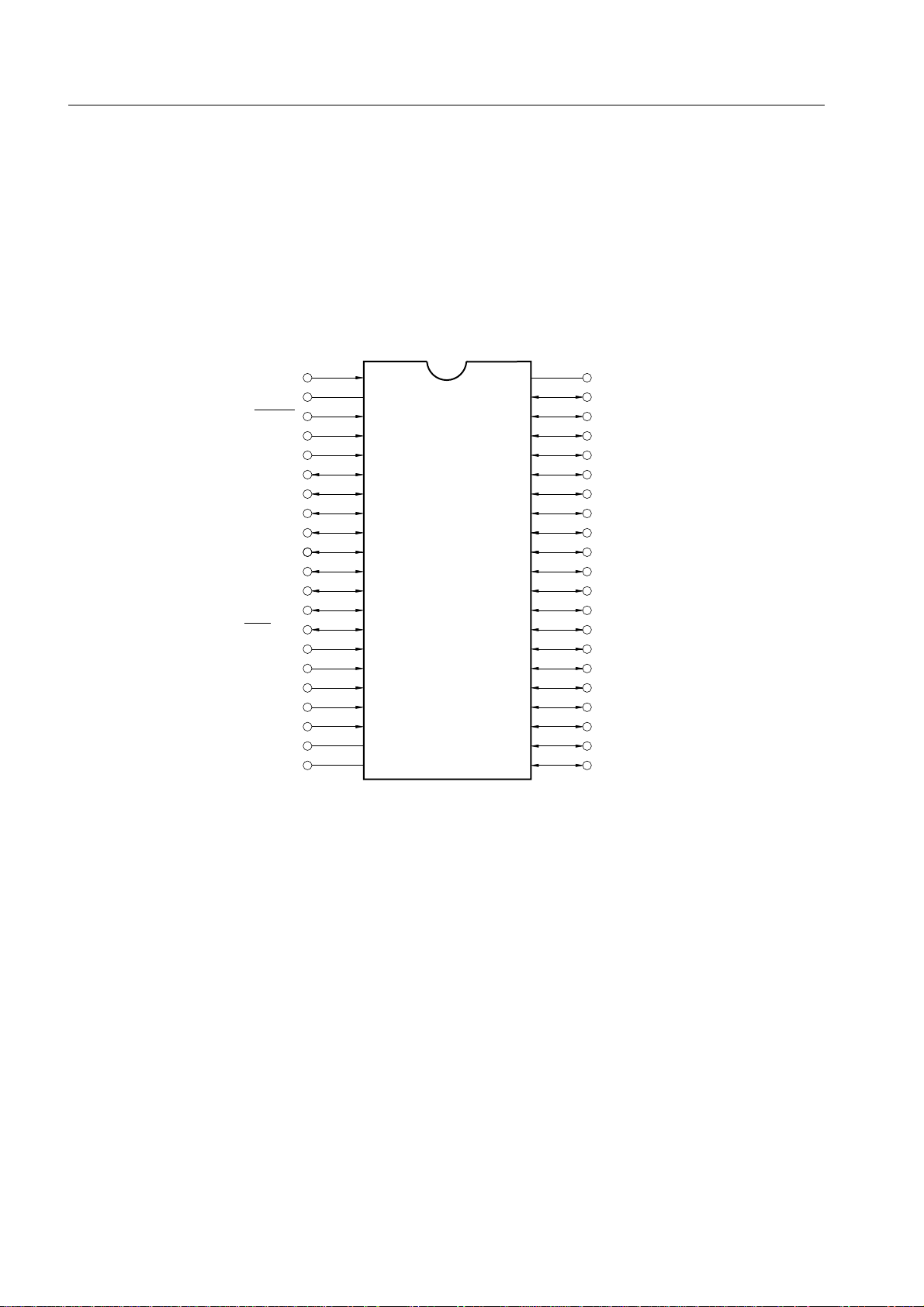
(1) 42-pin plastic shrink DIP (600 mil)
µPD750004CU-XXX
µPD750006CU-XXX
µPD750008CU-XXX
µPD75P0016CU
XT1
XT2
RESET
X1
X2
P33 (/MD3)
P32 (/MD2)
P31 (/MD1)
P30 (/MD0)
P81
P80
SI/SB1/P03
SO/SB0/P02
SCK/P01
INT4/P00
TI0/P13
INT2/P12
INT1/P11
INT0/P10
Note
PP
)
IC (V
V
1
2
3
4
5
6
7
8
9
10
11
12
13
14
15
16
17
18
19
DD
20
21
42
41
40
39
38
37
36
35
34
33
32
31
30
29
28
27
26
25
24
23
22
VSS
P40
P41
P42
P43
P50
P51
P52
P53
P60/KR0
P61/KR1
P62/KR2
P63/KR3
P70/KR4
P71/KR5
P72/KR6
P73/KR7
P20/PTO0
P21/PTO1
P22/PCL
P23/BUZ
Note Connect IC (VPP) to VDD, keeping the wiring as short as possible.
Remark ( ) : µPD75P0016.
6
Page 27
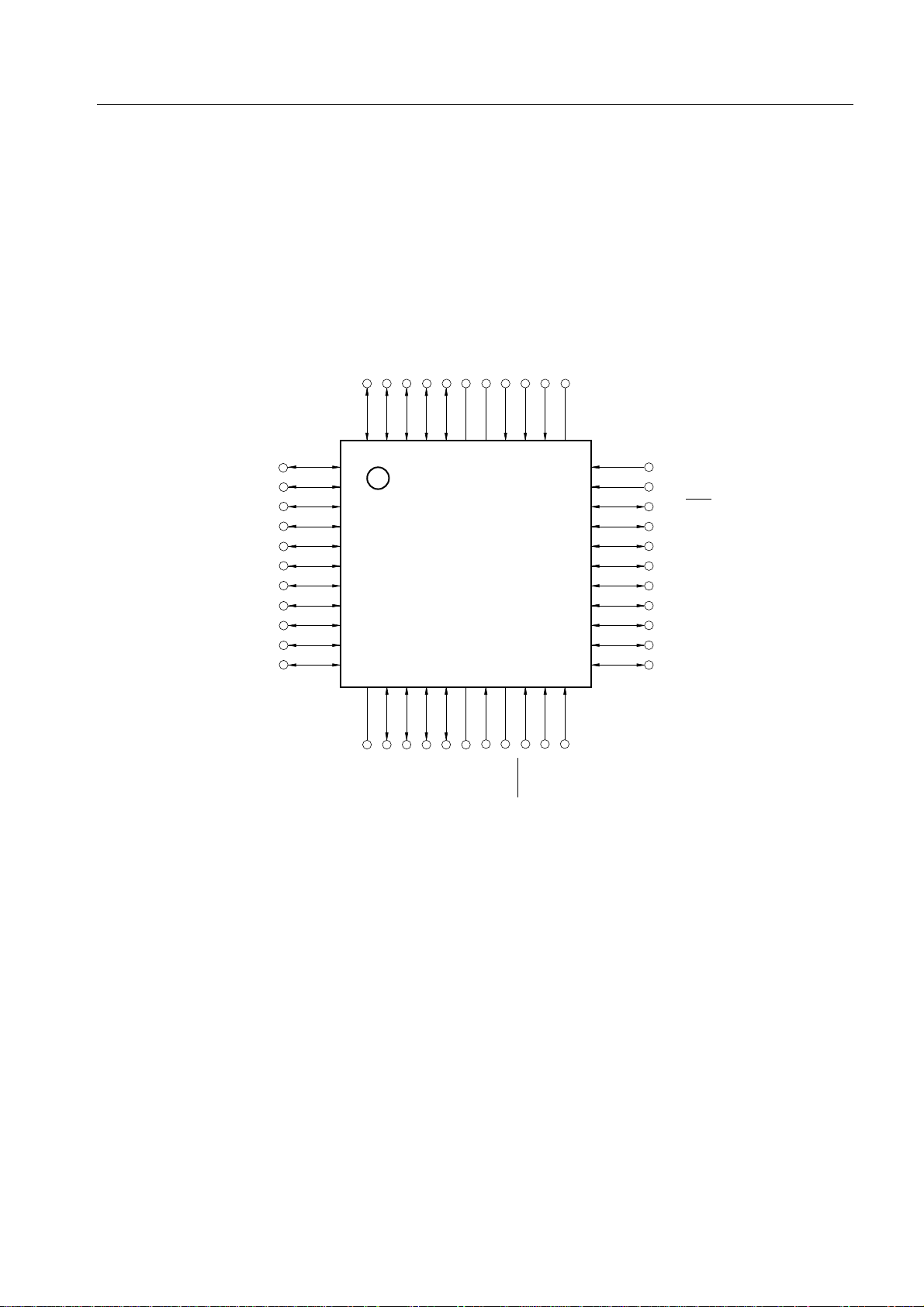
(2) 44-pin plastic QFP (10 x 10 mm)
µPD750004GB-XXX-3BS-MTX
µPD750006GB-XXX-3BS-MTX
µPD750008GB-XXX-3BS-MTX
µPD75P0016GB-3BS-MTX
P72/KR6
P71/KR5
P70/KR4
P63/KR3
P62/KR2
P61/KR1
P60/KR0
P53
P52
P51
P50
1
2
3
4
5
6
7
8
9
10
11
Note
)
PP
DD
P10/INT0
P11/INT1
P73/KR7
P20/PTO0
P21/PTO1
P22/PCL
P23/BUZ
V
IC (V
44 43 42 41 40 39 38 37 36 35 34
12 13 14 15 16 17 18 19 20 21 22
P12/INT2
NC
33
32
31
30
29
28
27
26
25
24
23
CHAPTER 1 GENERAL
P13/TI0
P00/INT4
P01/SCK
P02/SO/SB0
P03/SI/SB1
P80
P81
P30 (/MD0)
P31 (/MD1)
P32 (/MD2)
P33 (/MD3)
NC
P43
P42
P41
P40
SS
V
XT1
XT2
X1
RESET
X2
Note Connect IC (VPP) to VDD, keeping the wiring as short as possible.
Remark ( ) : µPD75P0016.
7
Page 28

µPD750008 USER'S MANUAL
Pin name
P00-P03 : Port 0 RESET : Reset input
P10-P13 : Port 1 TI0 : Timer input 0
P20-P23 : Port 2 PTO0, 1 : Programmable timer output 0, 1
P30-P33 : Port 3 BUZ : Buzzer clock
P40-P43 : Port 4 PCL : Programmable clock
P50-P53 : Port 5 INT0, 1, 4 : External vectored interrupt 0, 1, 4
P60-P63 : Port 6 INT2 : External test input 2
P70-P73 : Port 7 X1, 2 : Main system clock oscillation 1, 2
P80-P81 : Port 8 XT1, 2 : Subsystem clock oscillation 1, 2
KR0-KR7: Key return NC : No connection
SCK : Serial clock IC : Internally connected
SI : Serial input V
SO : Serial output V
SB0, 1 : Serial bus 0, 1 V
DD
SS
PP
: Positive power supply
: Ground
: Programming power supply
MD0-MD3 : Mode selection 0 - 3
8
Page 29
CHAPTER 2 PIN FUNCTIONS
2.1 PIN FUNCTIONS OF THE µPD750008
CHAPTER 2 PIN FUNCTIONS
Table 2-1. Digital I/O Port Pins (1/2)
Pin used Function circuit
Input/
output
Also
as
8 bit Upon
I/O reset
P00 Input INT4 4-bit input port (PORT0). x Input B
P01 I/O SCK For P01 to P03, built-in pull-up resistors F -A
P02 I/O SO/SB0 can be connected by software in units of F -B
P03 I/O SI/SB1 3 bits. M -C
P10 Input INT0 4-bit input port (PORT1). x Input B -C
P11 INT1 Built-in pull-up resistors can be connected
P12 INT2 by software in units of 4 bits. Only the
P13 TI0 P10/INT0 pin is provided with noise
elimination function.
P20 I/O PTO0 4-bit I/O port (PORT2). x Input E-B
P21 PTO1 Built-in pull-up resistors can be connected
P22 PCL by software in units of 4 bits.
P23 BUZ
P30
P31
P32
P33
Note 2
Note 2
Note 2
Note 2
I/O (MD0)
(MD1)
(MD2)
(MD3)
Note 3
Note 3
Note 3
Note 3
Programmable 4-bit I/O port (PORT3). x Input E-B
I/O can be specified bit by bit.
Built-in pull-up resistors can be connected
by software in units of 4 bits.
I/O
type
2
Note 1
Notes 1. I/O circuits enclosed in circles have a Schmitt-triggered input.
2. An LED can be driven directly.
3. ( ): µPD75P0016
9
Page 30
µPD750008 USER'S MANUAL
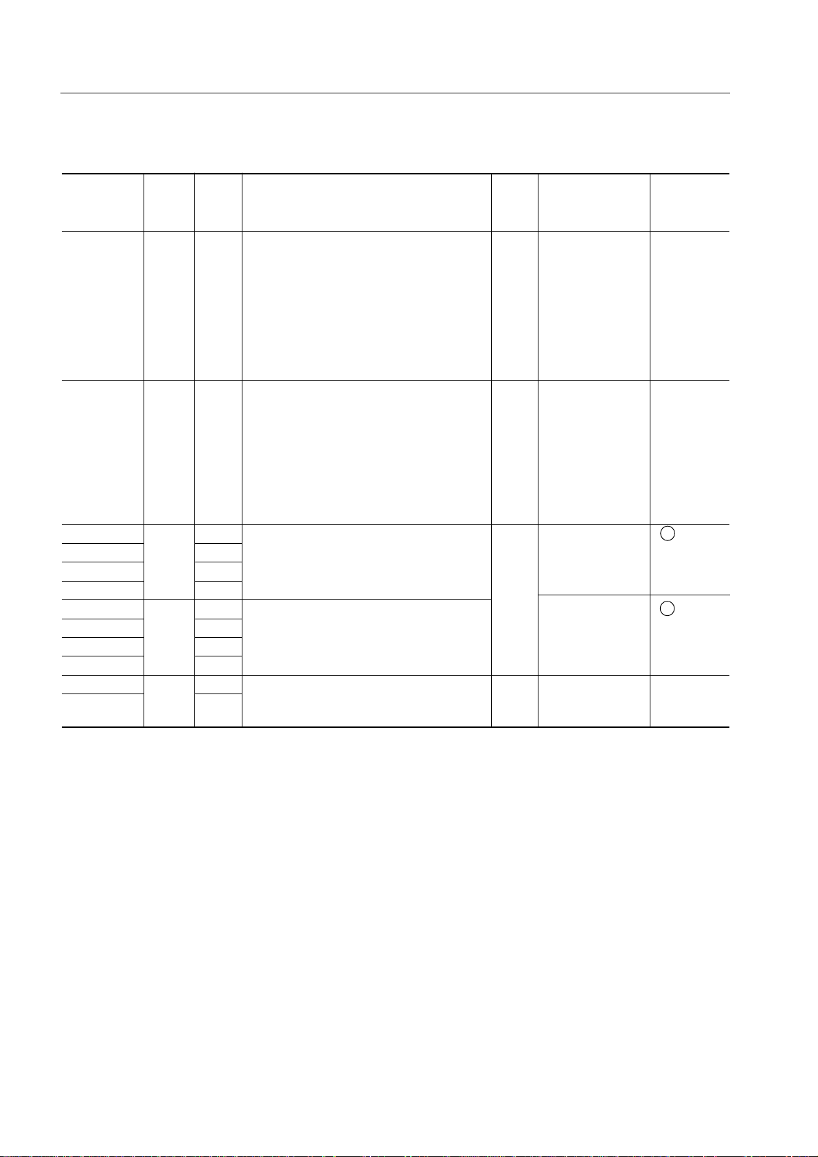
Table 2-1. Digital I/O Port Pins (2/2)
*
*
*
*
Pin
P40- I/O — N-ch open-drain 4-bit I/O port (PORT4). O High level (when M-D
Note 2, 4
P43
P50- I/O — N-ch open-drain 4-bit I/O port (PORT5). O High level (when M-D
Note 2, 4
P53
P60 I/O KR0 Programmable 4-bit I/O port (PORT6). O Input F -A
P61 KR1 I/O can be specified bit by bit.
P62 KR2 Built-in pull-up resistors can be
P63 KR3 connected by software in units of 4 bits.
P70 I/O KR4 4-bit I/O port (PORT7). Input F -A
P71 KR5 Built-in pull-up resistors can be
P72 KR6 connected by software in units of
P73 KR7 4 bits.
P80 I/O — 2-bit input port (PORT8). x Input E-B
P81 — Built-in pull-up resistors can be
Input
output
Also
used Function circuit
as
Withstand voltage is 13 V in open-drain a pull-up resistor (M-E)
mode. is provided) or
A pull-up resistor can be provided bit high impedance
Note 5
Note 5
.
.
by bit (mask option)
Data input/output pins for writing/
verifying (lower 4 bits of program
memory (PROM).
Withstand voltage is 13 V in open-drain a pull-up resistor (M-E)
mode. is provided) or
A pull-up resistor can be provided bit high impedance
by bit (mask option)
Data input/output pins for writing/
verifying (higher 4 bits of program
memory (PROM).
connected by software in units of 2 bits.
8 bit Upon
I/O reset
I/O
type
Note 1
Note 3
Note 3
*
*
Notes 1. I/O circuits enclosed in circles have a Schmitt-triggered input.
2. An LED can be driven directly.
3. ( ): µPD75P0016
4. When pull-up resistors that can be specified with the mask option are not
incorporated (when pins are used as N-ch open-drain input ports), the input leak low
current increases when an input instruction or bit operation instruction is executed.
5. These pins of the µPD75P0016 are not provided with pull-up resistors by mask option, and are
always open.
10
Page 31

Table 2-2. Non-Port Pin Functions
CHAPTER 2 PIN FUNCTIONS
Pin
TI0 Input P13 Inputs external event pulse to the timer/event counter — B -C
PTO0 I/O P20 Timer/event counter output Input E-B
PTO1 P21 Timer counter output
PCL I/O P22 Clock output Input E-B
BUZ I/O P23 Fixed frequency output Input E-B
SCK I/O P01 Serial clock I/O Input F -A
SO/SB0 I/O P02 Serial data output or serial data bus I/O Input F -B
SI/SB1 I/O P03 Serial data input or serial data bus I/O Input M -C
INT4 Input P00 Edge detection vectored interrupt input — B
INT0 Input P10 Edge detection vectored interrupt input Synchronous — B -C
INT1 P11 (The edge to be detected is selectable.) Asynchronous
INT2 Input P12 Rising edge detection testable input Asynchronous — B -C
KR0-KR3 I/O P60-P63 Parallel falling edge detection testable input Input F -A
KR4-KR7 I/O P70-P73 Parallel falling edge detection testable input Input F -A
X1, X2 Input — Connection pin to a crystal/ceramic resonator for main — —
XT1 Input — Connection pin to a crystal for subsystem clock — —
XT2 — When external clock is used, it is input to XT1, and
RESET Input — System reset input — B
Note 2
IC
V
DD
V
SS
Note 2
V
PP
Input/
output
— — Internally connected. — —
— — Positive power supply — —
— — GND potential — —
— P10/INT0 Program voltage application for program memory — —
Also
used Function
as type
(for buzzer or system clock trimming)
(Either a rising or falling edge is detected.)
The INT0/P10 pin has a noise eliminating function.
system clock generation.
When external clock is used, it is input to X1,
and its inverted signal is input to X2.
generation.
XT2 is left open.
Connect to VDD, keeping the wiring as short as possible.
(PROM) write/verify operation.
+12.5 V is applied for PROM write/verify operation.
Connect to VDD, keeping the wiring as short as
possible.
Upon
reset
I/O
circuit
Note 1
*
MD0- I/O P30-P33 Mode selection for program memory (PROM) Input E-B
Note 3
MD3
NC — — No connection — —
write/verify operation.
Notes 1. The circuits enclosed in circles have a Schmitt-triggered input.
2. Used as the VPP pin for the µPD75P0016.
3. Provided only in the µPD75P0016.
11
Page 32

µPD750008 USER'S MANUAL
2.2 PIN FUNCTION S
2.2.1 P00-P03 (PORT0) : Input Pins Used Also for INT4, SCK, SO/SB0 and SI/SB1
P10-P13 (PORT1) : Input Pins Used Also for INT0-INT2, and TI0
These are the input pins of the 4-bit input ports: Ports 0 and 1.
Ports 0 and 1 function as input ports, and also have the functions described below.
(1) Port 0 : Vectored interrupt input (INT4)
Serial interface I/O (SCK, SO/SB0, SI/SB1)
(2) Port 1 : Vectored interrupt input (INT0, INT1)
Edge detection test input (INT2)
External event pulse input (TI0) for timer/event counter
Input is always enabled for each pin of ports 0 and 1 regardless of the operation status of the other function
of the pin.
Schmitt-triggered inputs are used for the input pin of port 0 and pins of port 1 to prevent malfunction due
to noise. In addition, a noise eliminator is provided for P10. (See (3) of Section 6.3.)
Port 0 can be connected with built-in pull-up resistors in units of 3 bits (P01 to P03) by software. Port 1
can be connected with built-in pull-up resistors in units of 4 bits (P10 to P13) by software. This is done by
manipulating pull-up resistor specification register group A (POGA).
A RESET signal input places these pins in the input port mode.
12
Page 33

CHAPTER 2 PIN FUNCTIONS
2.2.2 P20-P23 (PORT2) : I/O Pins Used Also for PTO0, PTO1, PCL, and BUZ
P30-P33 (PORT3) : I/O Pins Used Also for MD0-MD3
P40-P43 (PORT4),
P50-P53 (PORT5) : N-ch Open-Drain Intermediate Withstand Voltage (13 V) Large-Current
Output
P60-P63 (PORT6),
P70-P73 (PORT7) : Tristate I/O
These pins are the I/O pins of the 4-bit I/O ports with output latches: Ports 2 to 7.
Port n (n = 2, 3, 6, and 7) functions as I/O ports, and also have the following functions:
(1) Port 2 : Timer/event counter (PTO0, PTO1)
Clock output (PCL)
Fixed frequency output (BUZ)
(2) Port 3 : Mode selection for program memory (PROM) write/verify operation (MD0-MD3)
(3) Ports 6 and 7: Key interrupt input (KR0-KR3, KR4-KR7)
Note Provided only in the µPD75P0016.
Note
*
Note
Port 3 is a large-current output. Ports 4 and 5 are N-ch open-drain intermediate withstand voltage (13 V)
large-current output. These ports can directly drive the LED.
An I/O mode is selected by the port mode register. The I/O mode of port m (m = 2, 4, 5, and 7) can be
selected in units of 4 bits, and the I/O mode of ports 3 and 6 can be selected bit by bit.
Port n can be connected with built-in pull-up resistors in units of 4 bits by software. This can be done by
manipulating pull-up resistor specification register group A (POGA). For ports 4 and 5, the use of built-in pullup resistors can be specified bit by bit by mask option.
Ports 4 and 5, and ports 6 and 7 can be paired respectively for 8-bit I/O.
A RESET input clears the output latches in the ports, places port n in the input mode (output highimpedance state), and drives ports 4 and 5 high if pull-up resistors are provided or causes ports 4 and 5
to go into a high-impedance state.
2.2.3 P80, P81 (PORT8)
These pins are the I/O pins of the 2-bit I/O ports with output latches: Port 8.
Port 8 can be connected with built-in pull-up resistors in units of 2 bits by software. This can be done by
manipulating pull-up resistor specification register group B (POGB).
2.2.4 TI0: Input Pin Used Also for Port 1
This is an external event pulse input pin for the programmable timer/event counter.
A Schmitt-triggered input is used for the TI0 pin.
*
2.2.5 PTO0, PTO1: Output Pin Used Also for Port 2
This is the output signal pin of the programmable timer/event counter and programmable timer counter.
Square-wave pulses appear on this pin. To output a signal from the programmable timer/event counter and
programmable timer counter, the output latch P20 or P21 must be cleared to 0, and the bit for port 2 in the
port mode register must be set to 1 (output mode).
The output is cleared to 0 by the timer start instruction.
13
Page 34

µPD750008 USER'S MANUAL
2.2.6 PCL: Output Pin Used Also for Port 2
This is the programmable clock output pin. It is used to supply the clock pulse to a peripheral LSI circuit
such as a slave microcomputer or A/D converter.
A RESET signal clears the clock mode register (CLOM) to 0, disabling clock output, then the pin is placed
in the normal mode to function as a normal port.
2.2.7 BUZ: Output Pin Used Also for Port 2
An arbitrary frequency (2.048, 4.096, or 32.768 kHz) output on this pin can be used for sounding the buzzer
or trimming the system clock frequency. This pin is used also as the P23 pin, and can be used only when
bit 7 (WM.7) of the clock mode register (WM) is set to 1.
A RESET signal places this pin in the normal operation mode as a general port (see Section 5.4.2 for
details).
2.2.8 SCK, SO/SB0, SI/SB1: Tristate I/O Pins Used Also as Port 0
These are I/O pins for serial interface. They operate according to the setting of the serial operation mode
registers (CSIM).
A RESET signal stops serial interface operation and places these pins in the input port mode.
A Schmitt-triggered input is used for each pin.
2.2.9 INT4: Input Pin Used Also as Port 0
INT4 is an external vectored interrupt input pin, which is rising edge active as well as falling edge active.
When a signal applied to this pin goes from low to high or from high to low, the interrupt request flag is set.
INT4 is an asynchronous input, and can accept a signal with some high level width or low level width
regardless of what the CPU clock is.
The INT4 pin can also be used to release the STOP and HALT modes. A Schmitt-triggered input is used
for this pin.
2.2.10 INT0, INT1: Input Pins Used Also for Port 1
These are edge detection vectored interrupt input pins. INT0 has a noise eliminator. The edge to be
detected can be selected using the edge detection mode registers (IM0, IM1).
(1) INT0 (bits 0 and 1 of IM0)
(a) Rising edge active
(b) Falling edge active
(c) Both rising and falling edges active
(d) External interrupt signal input disabled
(2) INT1 (bit 0 of IM1)
(a) Rising edge active
(b) Falling edge active
14
Page 35

CHAPTER 2 PIN FUNCTIONS
INT0 has a noise eliminator. Two different sampling clocks for noise elimination can be switched. The
acceptable width of a signal depends on the CPU clock.
INT1 is an asynchronous input, and can accept a signal with some high level width regardless of what the
CPU clock is.
A RESET input clears IM0 and IM1 to 0, selecting rising edge active.
The INT1 pin can also be used to release the STOP and HALT modes, but the INT0 pin cannot.
Schmitt-triggered inputs are used for the INT0 and INT1 pins.
2.2.11 INT2: Input Pin Used Also for Port 1
This is a rising edge active, external test input pin. When INT2 is selected with the edge detection mode
register (IM2), or when the signal applied to this pin goes high, the internal test flag (IRQ2) is set.
INT2 is an asynchronous input, and can accept a signal with some high level width regardless of the
operating clock of the CPU.
A RESET signal clears IM2 to 0. In this case, the test flag (IRQ2) is set by a rising edge on the INT2 pin.
The INT2 pin can also be used to release the STOP and HALT modes. A Schmitt-triggered input is used
for this pin.
2.2.12 KR0-KR3: Input Pins Used Also for Port 6
KR4-KR7: Input Pins Used Also for Port 7
KR0 to KR7 are key interrupt input pins. An interrupt is caused when parallel falling edges are detected
on them. The interrupt format can be specified with the edge detection mode register (IM2).
A RESET signal places these pins in the port 6 and 7 input modes.
2.2.13 X1, X2
These pins are used for connection to a crystal or ceramic resonator for main system clock generation.
An external clock can also be applied.
(a) Crystal/ceramic oscillation (b) External clock
µ
Crystal or ceramic resonator
PD750008
V
SS
X1
X2
(Standard frequency:
4.194304 or 6.0 MHz)
External
clock
PD74HC04
µ
µ
PD750008
X1
X2
15
Page 36

µPD750008 USER'S MANUAL
2.2.14 XT1, XT2
These pins are used for connection to a crystal for subsystem clock oscillation.
An external clock can also be applied.
(a) Crystal oscillation (b) External clock
µ
PD750008
V
SS
XT1
External
clock
µ
PD750008
XT1
Crystal
XT2
(Standard frequency:
32.768 kHz)
XT2
2.2.15 RESET
This is the pin for active-low reset input.
The RESET input is asynchronous. When a signal with certain low level width is applied to the pin, a RESET
signal is generated to cause a system reset, which has priority over any other operations.
The RESET signal is used for normal CPU initialize/start operation, and is also used to release the standby
(STOP or HALT) mode.
A Schmitt-triggered input is used for the RESET input pin.
2.2.16 V
DD
This is the positive power supply pin.
2.2.17 V
SS
This is the ground pin.
16
Page 37

CHAPTER 2 PIN FUNCTIONS
2.2.18 IC (for the µPD750004, µPD750006, and µPD750008 only)
The internally connected (IC) pin is used to set the µPD750008 to test mode for inspection prior to shipping.
In normal operation, connect the IC pin to the VDD pin, keeping the writing as short as possible.
When the wiring between the IC pin and the VDD pin is too long, or noise is generated on the IC pin, a potential
difference may occur between the IC pin and the VDD pin. This may cause your program to malfunction.
• Connect the IC pin to the VDD pin, keeping the wiring as short as possible.
Keep the wiring
as short as possible
IC (VPP)
V
V
DD
DD
2.2.19 VPP (for the µPD75P0016 only)
This is a program voltage input pin for program memory (PROM) write/verify operation.
For normal use, connect this pin to VDD, keeping the wiring as short as possible (shown above).
+12.5 V is applied for PROM write/verify operation.
2.2.20 MD0-MD3 (for the µPD75P0016 only): I/O Pins Used Also for Port 3
MD0 to MD3 select a mode for program memory (PROM) write/verify operation.
17
Page 38

µPD750008 USER'S MANUAL
2.3 PIN INPUT/OUTPUT CIRCUITS
Figure 2-1 shows schematic diagrams of the I/O circuitry of the µPD750008.
Figure 2-1. Pin Input/Output Circuits (1/2)
Type A
Type B
Type B-C
V
DD
P.U.R.
P-ch
P.U.R.: Pull-Up Resistor
P.U.R.
enable
IN
V
DD
P-ch
N-ch
CMOS input buffer
IN
Type D
V
DD
Data
IN
P-ch
OUT
Schmitt trigger input with hysteresis
Output
disable
Push-pull output which can be set to high-impedance output
(off for both P-ch and N-ch)
N-ch
18
Page 39

Type E-B
P.U.R.: Pull-Up Resistor
N-ch
(Withstand
voltage:13 V)
IN/OUT
Data
V
DD
Output
disable
P.U.R.
(Mask option)
Note
P.U.R
V
DD
P-ch
Input instruction
Input buffer with an intermediate
withstand voltage of +13 V
Pull-up resistor that operates only when an input
instruction is excuted (valid at low voltage)
Note
Data
Output
disable
IN/OUT
Note
P-ch
Input instruction
Input buffer with an intermediate
withstand voltage of +13 V
Note
V
DD
Pull-up resistor that operates only when an input
instruction is executed (valid at low voltage)
N-ch
(Withstand
voltage:13 V)
Figure 2-1. Pin Input/Output Circuits (2/2)
DD
V
Type M-C
CHAPTER 2 PIN FUNCTIONS
VDD
Data
Output
disable
Type F-A
Data
Output
disable
P.U.R.
enable
Type D
Type A
P.U.R.: Pull-Up Resistor
P.U.R.
enable
Type D
V
P.U.R.
P-ch
DD
P.U.R.
P-ch
IN/OUT
IN/OUT
Data
Output
disable
Type M-D*
P.U.R.
enable
N-ch
P.U.R.: Pull-Up Resistor
P.U.R.
P-ch
IN/OUT
Type F-B
Output
disable
(P-ch)
Data
Output
disable
Output
disable
(N-ch)
Type B
P.U.R.: Pull-Up Resistor
P.U.R.
enable
P.U.R.: Pull-Up Resistor
V
DD
Type M-E*
P.U.R.
P-ch
V
DD
P-ch
IN/OUT
N-ch
19
Page 40

µPD750008 USER'S MANUAL
2.4 CONNECTION OF UNUSED PINS
Table 2-3. Connection of Unused Pins
Pin name Recommended connection
P00/INT4 To be connected to V
P01/SCK To be connected to VSS or V
SS
DD
P02/SO/SB0
P03/SI/SB1
P10/INT0-P12/INT2 To be connected to V
SS
P13/TI0
P20/PTO0 Input state: To be connected to VSS or
P21/PTO1 VDD through a resistor
P22/PCL Output state: To be left open
P23/BUZ
P30(/MD0)-P33(/MD3)
Note
P40-P43
P50-P53
P60-P63
P70-P73
P80-P81
XT1 To be connected to VSS or V
XT2 To be left open
IC (VPP)
Note
To be connected directly to V
Note ( ): µPD75P0016
DD
DD
20
Page 41

CHAPTER 3 FEATURES OF THE ARCHITECTURE AND MEMORY MAP
CHAPTER 3 FEATURES OF THE ARCHITECTURE AND MEMORY MAP
The 75XL series architecture of the µPD750008 has the following features:
• Internal RAM of up to 4K words x 4 bits (12-bit address)
• Peripheral hardware expansibility
To provide these features, the following are used:
(1) Data memory bank structure
(2) General register bank structure
(3) Memory-mapped I/O
This chapter explains these topics.
3
3.1 DATA MEMORY BANK STRUCTURE AND ADDRESSING MODES
3.1.1 Data Memory Bank Structure
In the µPD750008, addresses 000H to 1FFH in data memory space are assigned to static RAM (512 words
x 4 bits), and addresses F80H to FFFH are assigned to peripheral hardware (such as I/O ports and timers).
To address a 12-bit location in this data memory space (4K x 4 bits), the µPD750008 uses such a memory
bank structure that the low-order eight bits are specified with an instruction directly or indirectly, and the highorder four bits are used to specify a memory bank.
To specify a memory bank (MB), two hardware items are incorporated:
• Memory bank enable flag (MBE)
• Memory bank select register (MBS)
The MBS is a register used to select a memory bank, and the register can be set to 0, 1, or 15. The MBE
is a flag used to determine whether the memory bank selected using the MBS is valid. As shown in Figure
3-1, when the MBE is set to 0, a certain memory bank is always selected regardless of the setting of the MBS.
When the MBE is set to 1, memory bank selection depends on the setting of the MBS, thus enabling data
memory space expansion.
In addressing data memory space, the MBE is usually set to 1 (MBE = 1), and data memory in the memory
bank specified in the MBS is operated. However, the MBE = 0 mode or MBE = 1 mode can be selected for
each step of processing for more efficient programming.
21
Page 42

µPD750008 USER'S MANUAL
Applicable program processing Effect
MBE = 0 mode • Interrupt processing MBS save/restoration becomes unnecessary.
• Processing that repeats internal MBS modification becomes unnecessary.
hardware and static RAM operations
• Subroutine processing MBS save/restoration becomes
MBE = 1 mode • Usual program processing
Figure 3-1. Use of MBE = 0 Mode and MBE = 1 Mode
<Main program>
SET1 MBE
<Subroutine>
MBE
= 1
CLR1 MBE
MBE = 0
RET <Interrupt processing>
; MBE = 0 is to be set in the vector table.
MBE = 0
RETI
Internal hardware
and static RAM
operations are
repeated.
CLR1 MBE
MBE
= 0
SET1 MBE
MEB
= 1
The contents of the MBE are automatically saved or restored at the time of subroutine processing, so that
the MBE can be freely modified during subroutine processing. In interrupt processing, the MBE is automatically
saved or restored, and when interrupt processing is started, the contents of the MBE can be specified for the
interrupt processing by setting the interrupt vector table. This speeds up interrupt processing.
The setting of the MBS can be modified for subroutine processing or interrupt processing by saving or
restoring the MBS with the PUSH or POP instruction.
The MBE is set using the SET1 or CLR1 instruction. The MBS is set using the SEL instruction.
Examples 1. The MBE is cleared, and a fixed memory bank is used.
CLR1 MBE ; MBE <– 0
22
2. Memory bank 1 is selected.
SET1 MBE ; MBE <– 1
SEL MB1 ; MBS <– 1
Page 43

CHAPTER 3 FEATURES OF THE ARCHITECTURE AND MEMORY MAP
3.1.2 Data Memory Addressing Modes
With the architecture of the µPD750008, seven addressing modes summarized in Figures 3-2 and 3-3, and
Table 3-1 are available to address data memory space efficiently for each bit length of data to be processed.
These addressing modes enable more efficient programming.
(1) 1-bit direct addressing (mem.bit)
In this addressing mode, the operand of an instruction can directly specify any bit in the entire data memory
space.
A particular memory bank (MB) is always used in this addressing mode. In the MBE = 0 mode, when an
address from 00H to 7FH is specified in the operand, memory bank 0 (MB = 0) is always used. When
an address from 80H to FFH is specified, memory bank 15 (MB = 15) is always used. Accordingly, both
the data area ranging from 000H to 07FH and the peripheral hardware area ranging from F80H to FFFH
can be addressed in the MBE = 0 mode.
In the MBE = 1 mode, MB = MBS, and specifiable data memory space can be expanded.
This addressing mode can be applied to four instructions: bit set and reset instructions (SET1 and CLR1),
and bit test instructions (SKT and SKF).
Example FLAG1 is set, FLAG2 is reset, and whether FLAG3 is zero is tested.
FLAG1 EQU 03FH.1 ; Bit 1 at address 3FH
FLAG2 EQU 087H.2 ; Bit 2 at address 87H
FLAG3 EQU 0A7H.0 ; Bit 0 at address A7H
SET1 MBE ; MBE <– 1
SEL MB0 ; MBS <– 0
SET1 FLAG1 ; FLAG1 <– 1
CLR1 FLAG2 ; FLAG2 <– 0
SKF FLAG3 ; FLAG3 = 0?
23
Page 44

µPD750008 USER'S MANUAL
Figure 3-2. Data Memory Organization and Addressing Range of Each Addressing Mode
000H
01FH
020H
07FH
0FFH
100H
1FFH
F80H
FC0H
Addressing mode
Memory bank enable flag
Data area
Static RAM
(memory bank 0)
Data area
Static RAM
(memory bank 1)
Not provided
Peripheral hardware area
(memory bank 15)
Area for
general register
MBE
=0
mem
mem.bit
MBE=1MBE=0MBE
MBS
=0
MBS
=1
MBS
=15
@HL
@H+mem.bit
=1
MBS
=0
MBS
=1
MBS
=15
@DE
@DL
Stack
address-
ing
————
SBS
SBS
fmem.bit pmem.@L
=0
=1
FFFH
Remark – : Don't care
24
Page 45

CHAPTER 3 FEATURES OF THE ARCHITECTURE AND MEMORY MAP
Table 3-1. Addressing Modes
Addressing mode
1-bit direct mem.bit Bit specified by bit at the address specified by MB and mem.
addressing • When MBE = 0 and
4-bit direct mem Address specified by MB and mem.
addressing • When MBE = 0 and
8-bit direct Address specified by MB and mem (mem: even address).
addressing • When MBE = 0 and
4-bit register @HL Address specified by MB and HL.
indirect @HL+ In this case, MB = MBE·MBS
addressing @HL– HL+ automatically increments the L register after addressing.
Representation
format
mem = 00H-7FH, MB = 0
mem = 80H-FFH, MB = 15
• When MBE = 1, MB = MBS
mem = 00H-7FH, MB = 0
mem = 80H-FFH, MB = 15
• When MBE = 1, MB = MBS
mem = 00H-7FH, MB = 0
mem = 80H-FFH, MB = 15
• When MBE = 1, MB = MBS
HL– automatically decrements the L register after addressing.
@DE Address specified by DE in memory bank 0
Specified address
@DL Address specified by DL in memory bank 0
8-bit register @HL Address specified by MB and HL. (Contents of the L register is
indirect an even address.)
addressing In this case, MB = MBE·MBS
Bit fmem.bit Bit specified by bit at the address specified by fmem.
manipulation In this case,
addressing fmem = FB0H-FBFH (interrupt-related hardware)
FF0H-FFFH (I/O ports)
pmem.@L Bit specified by the low-order two bits of the L register
at the address specified by the high-order 10 bits of pmem and the
high-order two bits of the L register.
In this case, pmem = FC0H-FFFH
@H+mem.bit Bit specified by bit at the address specified by MB, H, and the low-
order four bits of mem.
In this case, MB = MBE·MBS
Stack addressing — Address specified by the SP in memory bank selected by the SBS
25
Page 46

µPD750008 USER'S MANUAL
(2) 4-bit direct addressing (mem)
In this addressing mode, the operand of an instruction directly specifies any area in the data memory space
in units of four bits.
As with the 1-bit direct addressing mode, in the MBE = 0 mode, a fixed space consisting of the static RAM
area ranging from 000H to 07FH and the peripheral hardware area ranging from F80H to FFFH can be
addressed. In the MBE = 1 mode, MB = MBS, and specifiable data memory space can be expanded to
the entire space.
This addressing mode can be applied to the MOV, XCH, INCS, IN, and OUT instructions.
Caution Less efficient program processing results if data associated with an I/O port is stored in
the static RAM area of bank 1 as in Example 1. The modification of the MBS, as contained
in Example 2, becomes unnecessary in the programming if data associated with an I/O
port is stored at addresses 00H to 7FH of bank 0.
Examples 1. The data contained in BUFF is output on port 5.
BUFF EQU 11AH ; BUFF located at address 11AH
SET1 MBE ; MBE <– 1
SEL MB1 ; MBS <– 1
MOV A,BUFF ; A <– (BUFF)
SEL MB15 ; MBS <– 15
OUT PORT5,A ; PORT5 <– A
2. Data on port 4 is entered, and is saved in DATA1.
DATA1 EQU 5FH ; DATA1 located at address 5FH
CLR1 MBE ; MBE <– 0
IN A,PORT4 ; A <– PORT4
MOV DATA1,A ; (DATA1) <– A
(3) 8-bit direct addressing (mem)
In this addressing mode, the operand of an instruction directly specifies any area in the data memory space
in units of eight bits.
The operand can specify an even address. The 4-bit data at the address specified in the operand and
the 4-bit data at the address incremented by 1 are processed as a pair on an 8-bit basis with the 8-bit
accumulator (XA register pair).
A memory bank is specified in the same way as the 4-bit direct addressing.
This addressing mode can be applied to the MOV, XCH, IN, and OUT instructions.
Example 1. Eight-bit data from port 4 and port 5 is transferred to addresses 20H and 21H.
DATA EQU 020H
CLR1 MBE ; MBE <– 0
IN XA,PORT4 ; X <– PORT5 , A <– PORT4
MOV DATA,XA ; (21H) <– X, (20H) <– A
26
Page 47

CHAPTER 3 FEATURES OF THE ARCHITECTURE AND MEMORY MAP
Example 2. Eight-bit data is latched into the serial interface shift register (SIO), and the transfer data
is set at the same time.
SEL MB15 ; MBS <– 15
XCH XA,SIO ; XA <—> (SIO)
(4) 4-bit register indirect addressing (@rpa)
In this addressing mode, the pointer (general register pair) specified in the operand of an instruction
indirectly specifies a data memory space in units of four bits.
There are three types of data pointers. One is the HL register pair, which can specify any area in the data
memory space when MB = MBE·MBS is specified. The other two are the DE register pair and DL register
pair, with which memory bank 0 is always used regardless of how the MBE and MBS are specified. More
efficient programming is possible by selecting a data pointer according to a data memory bank to be used.
When the HL register pair is specified, the L register can be incremented or decremented by one in the
automatic increment or automatic decrement mode each time an instruction is executed, thus simplifying
the program step.
Example The data at 50H to 57H is transferred to 110H to 117H.
DATA1 EQU 57H
DATA2 EQU 117H
SET1 MBE ; MBE <– 1
SEL MB1 ; MBS <– 1
MOV D,#DATA1 SHR4 ; D <– 5
MOV HL,#DATA2 AND 0FFH ; HL <– 17H
LOOP: MOV A,@DL ; A <– (DL)
XCH A,@HL– ; A <—> (HL), L <– L – 1
BR LOOP
The addressing mode using the HL register pair as the data pointer finds a wide range of operations such
as data transfer, operations, comparison, and I/O. The addressing mode using the DE register pair or
DL register pair is applied to the MOV and XCH instructions.
This addressing mode, combined with an increment/decrement instruction for a general register or register
pair, enables data memory space addresses to be freely updated as shown in Figure 3-3.
Example 1. The data at 50H to 57H is compared with the data at 110H to 117H.
DATA1 EQU 57H
DATA2 EQU 117H
SET1 MBE
SEL MB1
MOV D,#DATA1 SHR4
MOV HL,#DATA2 AND 0FFH
LOOP: MOV A,@DL
SKE A,@HL ; A = (HL)?
BR NO ; NO
DECS L ; YES, L <– L – 1
BR LOOP
27
Page 48

µPD750008 USER'S MANUAL
Example 2. The data memory of 00H to FFH is cleared to 0.
CLR1 RBE
CLR1 MBE
MOV XA,#00H
MOV HL,#04H
LOOP: MOV @HL,A ; (HL) <– A
INCS HL ; HL <– HL + 1
BR LOOP
Figure 3-3. Updating Static RAM Addresses
0 x H
x 0H
DECS D
@DL
4-bit transfer
INCS D
DECS H
Automatic
decrement
DECS HL INCS HL
@HL
4-bit
manipulation
8-bit
manipulation
INCS LDECS L
Automatic
increment
INCS LDECS L
DECS DE INCS DE
Direct
addressing
Bit manipulation
4-bit transfer
8-bit transfer
x FH
DECS D
@DE
4-bit transfer
INCS D
DECS H
@H + mem.bit
Bit manipulation
INCS EDECS E
28
F x H
INCS H
INCS H
Page 49

CHAPTER 3 FEATURES OF THE ARCHITECTURE AND MEMORY MAP
(5) 8-bit register indirect addressing (@HL)
In this addressing mode, the data pointer (HL register pair) indirectly specifies any area in the data memory
space in units of eight bits.
The 4-bit data at the address determined with bit 0 of the data pointer (bit 0 of the L register) set to 0 and
the 4-bit data at the address incremented by 1 are processed as a pair on an 8-bit basis with the 8-bit
accumulator (XA register pair).
A memory bank is specified in the same way as the 4-bit register indirect addressing with the HL register
specified. In this case, MB = MBE·MBS.
This addressing mode can be applied to the MOV, XCH, and SKE instructions.
Examples 1. A comparison is made to determine whether the value of the count register (T0) of timer/
event counter 0 is equal to the data at addresses 30H and 31H.
DATA EQU 30H
CLR1 MBE
MOV HL,#DATA
MOV XA,T0 ; XA <– Count register 0
SKE XA,@HL ; XA = (HL)?
2. The data memory of 00H to FFH is cleared to 0.
CLR1 RBE
CLR1 MBE
MOV XA,#00H
MOV HL,#04H
LOOP: MOV @HL,XA ; (HL) <– XA
INCS HL
INCS HL
BR LOOP
(6) Bit manipulation addressing
This addressing mode is used to perform bit manipulations (such as Boolean operations and bit transfer)
for each bit in the data memory space.
The 1-bit direct addressing mode can be applied only to the set, reset, and test instructions. On the other
hand, the bit manipulation addressing enables a wide variety of bit manipulations such as Boolean
operations using the AND1, OR1, and XOR1 instructions, bit transfers using the MOV1 instruction, and
test and reset operations using the SKTCLR instruction.
There are three types of bit manipulation addressing. The user can choose from these options according
to the data memory address used.
29
Page 50

µPD750008 USER'S MANUAL
(a) Specific address bit direct addressing (fmem.bit)
In this addressing mode, peripheral equipment that frequently performs bit manipulations involving,
for example, I/O ports and interrupt flags, can be processed at all times regardless of memory bank
setting. Accordingly, the data memory addresses that allow this addressing mode to be used are FF0H
to FFFH where I/O ports are mapped, and FB0H to FBFH where interrupt-related hardware is mapped.
Hardware mapped to these data memory areas can freely perform bit manipulations in the direct
addressing mode at any time regardless of MBS and MBE setting.
Examples 1. Value input to P02 is inverted, and the result is output on P33.
MOV1 CY, PORT0.2
NOT1 CY
MOV1 PORT3.3, CY
2. The timer 0 interrupt request flag (IRQT0) is tested. The request flag, if set, is cleared,
and P63 is reset.
SKTCLR IRQT0 ; IRQT0 = 1?
BR NO ; NO
CLR1 PORT6.3 ; YES
3. If both P30 and P41 are set to 1, P53 is reset.
P30
P41
P53
MOV1 CY, PORT3.0 ; CY <– P30
AND1 CY, PORT4.1 ; CY P41
NOT1 CY ; CY <– CY
MOV1 PORT5.3, CY ; P53 <– CY
30
Page 51
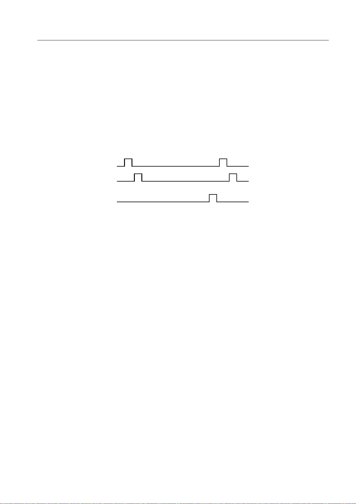
CHAPTER 3 FEATURES OF THE ARCHITECTURE AND MEMORY MAP
(b) Specific address bit register indirect addressing (pmem.@L)
In this addressing mode, the bits of peripheral hardware I/O ports are indirectly specified using a
register to allow continuous manipulations. This addressing mode can be applied to data memory
addresses FC0H to FFFH.
In this addressing mode, the high-order 10 bits of a 12-bit data memory address is directly specified
in the operand, and the low-order two bits and bit address are indirectly specified using the L register.
Thus the use of the L register enables 16 bits (four ports) to be continuously manipulated.
This addressing mode again enables bit manipulation regardless of MBE and MBS setting.
Example Pulses are output on the bits in the order from port 4 to port 7.
P40
P41
·
·
·
P73
·
·
·
MOV L,#0
LOOP: SET1 PORT4.@L ; Bits (L
CLR1 PORT4.@L ; Bits (L
INCS L
NOP
BR LOOP
) of ports 4 to 7 <– 1
1-0
) of ports 4 to 7 <– 0
1-0
31
Page 52

µPD750008 USER'S MANUAL
(c) Specific 1-bit direct addressing (@H+mem.bit)
This addressing mode enables any bit in the data memory space to be manipulated.
In this addressing mode, the high-order four bits of the data memory address in the memory bank
specified by MB = MBE·MBS are indirectly specified using the H register, and the low-order four bits
and bit address are directly specified in the operand. This addressing mode enables a wide variety
of manipulations for each bit in the entire data memory space.
Example Bit 2 at address 32H (FLAG3) is reset if both bit 3 at address 30H (FLAG1) and bit 0 at
address 31H (FLAG2) are set to 0 or 1.
FLAG1
FLAG2
FLAG1 EQU 30H.3
FLAG2 EQU 31H.0
FLAG3 EQU 32H.2
SEL MB0
MOV H,#FLAG1 SHR 6
MOV1 CY, @H+FLAG1 ; CY <– FLAG1
XOR1 CY, @H+FLAG2 ; CY <– CY FLAG2
MOV1 @H+FLAG3, CY ; FLAG3 <– CY
FLAG3
32
Page 53

CHAPTER 3 FEATURES OF THE ARCHITECTURE AND MEMORY MAP
(7) Stack addressing
This addressing mode is used for save/restoration operation in interrupt processing or subroutine
processing.
In this addressing mode, the address indicated by the stack pointer (8 bits) of data memory bank 0 is
specified.
This addressing mode can be used for register save/restoration operation using the PUSH or POP
instruction as well as save/restoration operation in interrupt and subroutine processing.
Examples 1. A register is saved and restored in subroutine processing.
SUB: PUSH XA
PUSH HL
PUSH BS ; Save MBS and RBS
POP BS
POP HL
POP XA
RET
·
·
·
2. The contents of the HL register pair are transferred to the DE register pair.
PUSH HL
POP DE ; DE <– HL
3. A branch is made to the address indicated by the [XABC] register.
PUSH BC
PUSH XA
RET ; Branch to address XABC
33
Page 54

µPD750008 USER'S MANUAL
3.2 GENERAL REGISTER BANK CONFIGURATION
The µPD750008 contains four register banks, each consisting of eight general registers: X, A, B, C, D,
E, H, and L. These registers are mapped to addresses 00H to 1FH in memory bank 0 of the data memory
(see Figure 3-5). To specify a general register bank, a register bank enable flag (RBE) and a register bank
select register (RBS) are contained. The RBS is a register used to select a register bank, and the RBE is
a flag used to determine whether a register bank selected using the RBS is to be enabled. The register bank
(RB) enabled at instruction execution is determined as
RB = RBE·RBS
Table 3-2. Register Bank to Be Selected with the RBE and RBS
RBE
3210
000xx
100
RBS
01
Always 0
Register bank
Bank 0 is always selected.
Bank 0 is selected.00
Bank 1 is selected.
Bank 2 is selected.10
Bank 3 is selected.11
Remark x: Don’t care
The contents of the RBE are automatically saved or restored at the beginning or end of subroutine
processing, so that the RBE can be freely modified during subroutine processing. In interrupt processing,
the RBE is automatically saved or restored, and when interrupt processing is started, the contents of the RBE
can be specified for the interrupt processing by setting the interrupt vector table. Therefore, as indicated in
Table 3-3, by selecting a register bank depending on whether the processing is normal or interrupt, the general
register need not be saved and restored for the level-one interrupt processing, and only the RBS needs to
be saved and restored for the level-two interrupt processing, thus speeding up interrupt processing.
Table 3-3. Recommended Use of Register Banks with Normal Routines and Interrupt Routines
Normal processing Use register banks 2 and 3 with RBE = 1.
Level-one interrupt processing Use register bank 0 with RBE = 0.
Level-two interrupt processing Use register bank 1 with RBE = 1.
(In this case, the RBS needs to be saved and restored.)
Multiple (triple or more) interrupt processing Save and restore the registers with PUSH or POP.
34
Page 55

<Main program>
SET1 RBE
SEL RB2
CHAPTER 3 FEATURES OF THE ARCHITECTURE AND MEMORY MAP
Figure 3-4. Example of Register Bank Selection
<Level-one interrupt>
; RBE = 0 in the
vector table
RB = 2
RB = 0
RETI
<Level-two interrupt>
; RBE = 1 in the
vector table
PUSH BS
SEL RB1
RB = 1
POP BS
RETI
<Level-three interrupt>
; RBE = 0 in the
vector table
PUSH rp
RB = 0
POP rp
RETI
The setting of the RBS can be modified for subroutine processing or interrupt processing by saving or
restoring the RBS with the PUSH or POP instruction.
The RBE is set using the SET1 or CLR1 instruction. The RBS is set using the SEL instruction.
Example
SET1 RBE ; RBE <– 1
CLR1 RBE ; RBE <– 0
SEL RB0 ; RBS <– 0
SEL RB3 ; RBS <– 3
The general register area of the µPD750008 can be used not only on a 4-bit basis, but also on an 8-bit
basis with register pairs. This enables users to perform transfers, arithmetic/logical operations, comparisons,
and increments and decrements at a speed comparable to that of an 8-bit microcomputer, and thereby enables
to program using mainly general registers.
(1) When used as a 4-bit register
When the general register area is used on a 4-bit basis, eight general registers, the X, A, B, C, D, E, H,
and L registers, are available in the register bank specified with RB = RBE·RBS as shown in Figure 3-
5. The A register functions as a 4-bit accumulator which performs transfers, arithmetic/logical operations,
and comparisons. The other general registers perform transfers, comparisons, and increments/decrements
with the accumulator.
35
Page 56

µPD750008 USER'S MANUAL
(2) When used as an 8-bit register
When the general register area is used on an 8-bit basis, the register pairs in the register bank specified
by RBE·RBS can be specified as XA, BC, DE, and HL as shown in Figure 3-6, and the register pairs in
the register bank that has the inverted value of bit 0 of the register bank (RB) can be specified as XA’,
BC’, DE’, and HL’, thus providing up to eight 8-bit registers. The XA register pair functions as an 8-bit
accumulator which performs transfers, arithmetic/logical operations, comparisons, and increments/
decrements of 8-bit data. The other register pairs perform transfers, arithmetic/logical operations,
comparisons, and increments/decrements with the accumulator. The HL register pair functions mainly
as a data pointer, and the DE and DL register pairs function as an auxiliary data pointer.
Examples 1. INCS HL ; HL <– HL + 1, skip at HL = 00H
ADDS XA,BC ; XA <– XA + BC, skip at carry
SUBC DE’,XA ; DE’ <– DE’ – XA – CY
MOV XA,XA’ ; XA <– XA’
MOVT XA,@PCDE ; XA <– (PC
+ DE) ROM, reference table
12-8
SKE XA, BC ; Skip if XA = BC
2. The value of the count register (T0) for timer/event counter 0 is tested until it becomes
greater than the value of the BC’ register pair.
CLR1 MBE
NO: MOV XA,T0 ; Read count register
SUBS XA,BC’ ; XA • BC?
BR YES ; YES
BR NO ; NO
36
Page 57

CHAPTER 3 FEATURES OF THE ARCHITECTURE AND MEMORY MAP
Figure 3-5. General Register Configuration (4-bit Processing)
X
H
D
B
X
H
D
B
X
H
D
01H
03H
05H
07H
09H
0BH
0DH
0FH
11H
13H
15H
A
L
E
C
A
L
E
C
A
L
E
00H
02H
04H
06H
08H
0AH
0CH
0EH
10H
12H
14H
Register bank 0
(RBE·RBS = 0)
Register bank 1
(RBE·RBS = 1)
Register bank 2
(RBE·RBS = 2)
B
X
H
D
B
17H
19H
1BH
1DH
1FH
C
A
L
E
C
16H
18H
1AH
1CH
1EH
Register bank 3
(RBE·RBS = 3)
37
Page 58

µPD750008 USER'S MANUAL
Figure 3-6. General Register Configuration (8-bit Processing)
XA
HL
DE
BC
XA’
HL’
DE’
BC’
XA
HL
00H
02H
04H
06H
When RBE·RBS
= 0
08H
0AH
0CH
0EH
10H
12H
XA’
HL’
DE’
BC’
XA
HL
DE
BC
XA’
HL’
00H
02H
04H
06H
When RBE·RBS
= 1
08H
0AH
0CH
0EH
10H
12H
DE
BC
XA’
HL’
DE’
BC’
14H
16H
When RBE·RBS
= 2
18H
1AH
1CH
1EH
DE’
BC’
XA
HL
DE
BC
14H
16H
When RBE·RBS
= 3
18H
1AH
1CH
1EH
38
Page 59

CHAPTER 3 FEATURES OF THE ARCHITECTURE AND MEMORY MAP
3.3 MEMORY-MAPPED I/O
The µPD750008 employs memory-mapped I/O, which maps peripheral hardware such as timers and I/O
ports to addresses F80H to FFFH in data memory space as shown in Figure 3-2. This means that there is
no particular instruction to control peripheral hardware, but all peripheral hardware is controlled using memory
manipulation instructions. (Some mnemonics for hardware control are available to make programs readable.)
To manipulate peripheral hardware, the addressing modes listed in Table 3-4 can be used.
Table 3-4. Addressing Modes Applicable to Peripheral Hardware Operation
Applicable addressing mode Applicable hardware
Bit Direct addressing mode specifying mem.bit with All hardware
manipulation MBE = 0 (MBE = 1, MBS = 15) allowing bit manipulation
Direct addressing mode specifying fmem.bit regardless of IST1, IST0, MBE, RBE,
MBE and MBS setting IExxx, IRQxxx, PORTn.x
Indirect addressing mode specifying pmem.@L regardless of BSBn.x
MBE and MBS setting PORTn.x
4-bit Direct addressing mode specifying mem with All hardware allowing 4-bit
manipulation MBE = 0 or (MBE = 1, MBS = 15) manipulation
Register indirect addressing mode specifying @HL with
(MBE = 1, MBS = 15)
8-bit Direct addressing mode specifying mem (even address) with All hardware allowing 8-bit
manipulation MBE = 0 or (MBE = 1, MBS = 15) manipulation
Register indirect addressing mode specifying @HL
(with the L register containing an even number) with
MBE = 1 and MBS = 15
Figure 3-7 summarizes the I/O map of the µPD750008.
The items in the figure have the following meanings:
• Symbol : Name representing incorporated hardware, which can be coded in the operand field of an
instruction
• R/W : Indicates whether the hardware allows read/write operation.
R/W : Both read and write operations possible
R : Read only
W : Write only
• Number of manipulatable bits:
Indicates the number of bits that can be processed at a time in hardware manipulation
O : Bit manipulation is possible in units of the indicated number of bits (1, 4, or 8 bits).
Ð : Particular bits can be manipulated. For these bits, see Remarks.
– : Bit manipulation is impossible in units of the indicated number of bits (1, 4, or 8 bits).
• Bit manipulation addressing:
Bit manipulation addressing applicable in hardware bit manipulation
39
Page 60

µPD750008 USER'S MANUAL
Figure 3-7. µPD750008 I/O Map (1/5)
Hardware name (symbol)
Address
b3 b2 b1 b0
F80H
Stack pointer (SP)
F82H
F83H
F84H Stack bank selection register (SBS) R/W – mem.bit–
F85H
F86H
F8BH
F98H
Register bank selection register (RBS)
Bank selection register (BS)
Memory bank selection register (MBS)
Basic interval timer mode register (BTM)
Basic interval timer (BT)
Note 2
WDTM
Clock mode register (WM) R/W
R/W
R/W
R
W
R
W
Number of bits that can be
manipulated
1 bit 4 bits 8 bits
––
–
–
–
––
––
(R)
––
–
Bit
manipulation
addressing
–
–
mem.bit
–
mem.bit
mem.bit
–
Remarks
Bit 0 is fixed
to 0.
Note 1
Only bit 3 can
be manipulated.
Only bit 3 can
be tested.
Notes 1. Can be manipulated separately as the RBS and MBS in 4-bit units.
Can also be manipulated as the BS in 8-bit units.
Use SEL MBn and SEL RBn instructions to write data to MBS and RBS respectively.
2. WDTM: Watchdog timer enable flag (W); cannot be cleared by an instruction.
40
Page 61

CHAPTER 3 FEATURES OF THE ARCHITECTURE AND MEMORY MAP
Figure 3-7. µPD750008 I/O Map (2/5)
Address
FA0H
FA2H
FA4H
FA6H
FA8H
FAAH
Hardware name (symbol)
b3 b2 b1 b0
Timer/event counter mode register (TM0)
Note 1
TOE0
Timer/event counter count register (T0) R – –
Timer/event counter modulo register (TMOD0) R/W – –
Timer counter mode register (TM1)
Note 2
TOE1
Number of bits that can be
manipulated
R/W
1 bit 4 bits 8 bits
R/W
W––mem.bit
R/W
W––mem.bit
(W)
––
(W)
––
Bit
manipulation
addressing
–
(R/W)
–
(R/W)
–
mem.bit
–
–
–
mem.bit
Remarks
Bit write manipu-
lation is enabled
only for bit 3.
Bit write manipu-
lation is enabled
only for bit 3.
FACH
Timer counter count register (T1) R – –
FAEH
Timer counter modulo register (TMOD1) R/W – –
Notes 1. TOE0: Timer/event counter output enable flag (W)
2. TOE1: Timer counter output enable flag (W)
–
–
41
Page 62

µPD750008 USER'S MANUAL
Figure 3-7. µPD750008 I/O Map (3/5)
Address
FB0H
FB2H
FB3H
FB4H
FB5H
FB6H
FB7H
FB8H
FBAH
FBCH
FBDH
Hardware name (symbol)
b3 b2 b1 b0
IST1
Program status word (PSW)
CY
Interrupt priority select register (IPS)
Processor clock control register (PCC)
INT0 edge detection mode register (IM0)
INT1 edge detection mode register (IM1)
INT2 edge detection mode register (IM2)
System clock control register (SCC)
IE4
IET1
IST0
SK2
IRQ4
IRQT1
MBE
SK1
IEBT
IEW
IET0
IECSI
IRQBT
IRQW
IRQT0
IRQCSI
RBE
SK0
Number of bits that can be
manipulated
R/W
1 bit 4 bits 8 bits
R/W
R/W
R/W
R/W
R/W –
R/W
R/W
R/W
R/W
R/W
R/W
(R/ W)
(R/W)
(R/W)
–
–
–
–
–
–
–
(R)
(R)
–
–
–
–
–
Bit
manipulation
addressing
fmem.bit
–
–
fmem.bit
Remarks
Manipulation in
8-bit units is
enabled only
for reading.
Note 1
Note 2
Bits 3, 2, and 1
are fixed to 0.
Bits 3 and 2 are
fixed to 0.
Bits 2 and 1 are
fixed to 0.
FBEH
FBFH
FC0H
FC1H
FC2H
FC3H
FCFH R/WSub-oscillator control register (SOS)
IE1
Bit sequential buffer 0 (BSB0)
Bit sequential buffer 1 (BSB1)
Bit sequential buffer 2 (BSB2)
Bit sequential buffer 3 (BSB3)
IRQ1
IE0
IE2
IRQ0
IRQ2
R/W
R/W
R/W
R/W
R/W
R/W
–
Remarks 1. IExxx : Interrupt enable flag
2. IRQxxx: Interrupt request flag
Notes 1. Only bit 3 can be manipulated by an EI/DI instruction.
2. Bits 3 and 2 can be manipulated bit by bit by a STOP/HALT instruction.
–
mem.bit
pmem.@L
––
42
Page 63

CHAPTER 3 FEATURES OF THE ARCHITECTURE AND MEMORY MAP
Figure 3-7. µPD750008 I/O Map (4/5)
Address
FD0H
FDCH
FDEH
FE0H
FE2H
FE4H
Hardware name (symbol)
b3 b2 b1 b0
Clock output mode register (CLOM)
Pull-up resistor specification register group A
(POGA)
Pull-up resistor specification register group B
(POGB)
Serial operation mode register (CSIM)
CSIE COI WUP
CMDD
SBI control register (SBIC)
BSYE
RELD
ACKD
CMDT
ACKE
RELT
ACKT
Number of bits that can be
manipulated
R/W
1 bit 4 bits 8 bits
– –R/W
R/W –
R/W ––
R/W
(R) (W)
R/W
R/W –– –Serial I/O shift register (SIO)
Bit
manipulation
addressing
–
––
–
––
–
– – mem.bit
–
mem.bit
Remarks
Note
Whether this
location is read-
or write-
accessible de-
pends on the bit.
FE6H
–
FE8H
FECH
FEEH
PM33
Port mode register group A (PMGA)
PM63
–
Port mode register group B (PMGB)
PM7
–
Port mode register group C (PMGC)
–
PM32
PM62
PM2
–
–
–
PM31
PM61
–
PM5
–
–
R/W –
PM30
R/W
PM60
–
R/W
PM4
PM8
R/W
–
Note Whether a bit can be read or written depends on the bit.
–Slave address register (SVA)
––
––
––
–
–
–
43
Page 64

µPD750008 USER'S MANUAL
Figure 3-7. µPD750008 I/O Map (5/5)
Number of bits that can be
manipulated
R/W
1 bit 4 bits 8 bits
R/W
(R) (R/W)
R
R/W
R/W
R/W
R/W
R/W
R/W
R/W
(R)
–
–
–
Bit
manipulation
addressing
fmem.bit
pmem.@L
Remarks
Note 1
Address
FF0H
FF1H
FF2H
FF3H
FF4H
FF5H
FF6H
FF7H
FF8H
Port 0
Port 1
Port 2
Port 3
Port 4
Port 5
Note 2
Port 6
Note 2
Port 7(PORT7)
Port 8
Hardware name (symbol)
b3 b2 b1 b0
(PORT0)
(PORT1)
(PORT2)
(PORT3)
(PORT4)
(PORT5)
KR3 KR2 KR1
(PORT6)
KR7
KR6 KR5 KR4
(PORT8)
SCKP
KR0
Notes 1. Bit 1 can be read or written only in serial operation enable mode. It can be read when four-bit
manipulation is performed.
2. KR0 to KR7 can be read (R) bit by bit. When inputting 4 bits at a time, specify PORT6 or PORT7.
44
Page 65

CHAPTER 4 INTERNAL CPU FUNCTIONS
CHAPTER 4 INTERNAL CPU FUNCTIONS
4.1 Mk I MODE/Mk II MODE SWITCH FUNCTIONS
4.1.1 Differences between Mk I Mode and Mk II Mode
The CPU of the µPD750008 subseries has two modes (Mk I mode and Mk II mode) and which mode is
used is selectable. Bit 3 of the stack bank selection register (SBS) determines the mode.
• Mk I mode: This mode has the upward compatibility with the µPD75008 subseries.
It can be used in the 75XL CPUs having a ROM of up to 16KB.
• Mk II mode: This mode is not compatible with the µPD75008 subseries.
It can be used in all 75XL CPUs, including those having a ROM of 16KB or more.
Table 4-1 shows the differences between Mk I mode and Mk II mode.
4
Table 4-1. Differences between Mk I Mode and Mk II Mode
Mk I mode Mk II mode
Number of stack bytes in a subroutine instruction 2 bytes 3 bytes
BRA !addr1 instruction Undefined operation Normal operation
CALLA !addr1 instruction
CALL !addr instruction 3 machine cycles 4 machine cycles
CALLF !faddr instruction 2 machine cycles 3 machine cycles
Caution Mk II mode is for maintaining a software compatibility with products in the 75X series or
75XL series whose program memory is more than 24K bytes.
Therefore, Mk I mode is recommended for applications with a focus on the ROM efficiency
or speed.
*
45
Page 66

µPD750008 USER'S MANUAL
4.1.2 Setting of the Stack Bank Selection Register (SBS)
The Mk I mode and Mk II mode are switched by stack bank selection register. Figure 4-1 shows the register
configuration.
The stack bank selection register is set with a 4-bit memory operation instruction. To use the CPU in Mk
I mode, initialize the register to 10xxB
initialize it to 00xxB
Note
.
Note
at the beginning of the program. To use the CPU in Mk II mode,
Figure 4-1. Stack Bank Selection Register Format
Address
F84H
0123
Symbol
SBS0SBS1SBS2SBS3
SBS
Stack area designation
0001Memory bank 0
Memory bank 1
Other settings are inhibited
Bit 2 must be set to 0
Mode switching designation
01Mk II mode
Mk I mode
Note Specify the desired value in xx.
Caution The CPU operates in Mk I mode after the RESET signal is issued, because bit 3 of SBS
is set to 1. Set bit 3 of SBS to 0 (Mk II mode) to use the CPU in Mk II mode.
46
Page 67

CHAPTER 4 INTERNAL CPU FUNCTIONS
4.2 PROGRAM COUNTER (PC):
12 BITS (µPD750004)
13 BITS (µPD750006 AND µPD750008)
14 BITS (µPD75P0016)
The program counter is a binary counter which retains the address data of the program memory. The
program counter consists of 12 bits in the µPD750004 (see Figure 4-2(a) ), 13 bits in the µPD750006 and
µPD750008 (see Figure 4-2(b)), and 14 bits in the µPD75P0016 (see Figure 4-2(c)).
Figure 4-2. Program Counter Organization
(a) µPD750004
PC10 PC9 PC8 PC7 PC6 PC5 PC4 PC3 PC2 PC1 PC0PC11
(b) µPD750006 and µPD750008
PC11 PC10 PC9 PC8 PC7 PC6 PC5 PC4 PC3 PC2 PC1 PC0PC12
(c) µPD75P0016
PC12 PC11 PC10 PC9 PC8 PC7 PC6 PC5 PC4 PC3 PC2 PC1 PC0PC13
Usually, each time an instruction is executed, the program counter is automatically incremented according
to the number of bytes in the instruction.
When a branch instruction (BR, BRA, BRCB) is executed, immediate data indicating the branch destination
and the contents of a register pair are set in all or some bits of the program counter.
When a subroutine call instruction (CALL, CALLA, CALLF) is executed, or a vectored interrupt occurs, the
current contents of the program counter (already incremented return address for fetching the next instruction)
are saved in the stack memory (data memory indicated by the stack pointer), then the jump destination address
is loaded.
When a return instruction (RET, RETS, RETI) is executed, the contents of the stack memory are set in the
program counter.
When the RESET signal is issued, the program counter is initialized to the contents of the program memory
at addresses 000H and 001H. The program can be started from any address according to the contents.
µPD750004 :
PC11-PC8 <– (000H)
, PC7-PC0 <– (001H)
3-0
7-0
µPD750006 and µPD750008 :
PC12-PC8 <– (000H)
, PC7-PC0 <– (001H)
4-0
µPD75P0016 :
PC13-PC8 <– (000H)
, PC7-PC0 <– (001H)
5-0
7-0
7-0
47
Page 68

µPD750008 USER'S MANUAL
4.3 PROGRAM MEMORY (ROM):
4096 WORDS x 8 BITS (µPD750004: MASKED ROM)
6144 WORDS x 8 BITS (µPD750006: MASKED ROM)
8192 WORDS x 8 BITS (µPD750008: MASKED ROM)
16384 WORDS x 8 BITS (µPD75P0016: ONE-TIME PROM)
The program memory is used for storing programs, an interrupt vector table, GETI instruction reference
table, table data, and so forth. The µPD750004, µPD750006, and µPD750008 are provided with a maskprogrammable ROM as the program memory, and the µPD75P0016 is provided with a one-time PROM.
Figures 4-3 to 4-6 show the program memory maps.
Program memory is addressed by the program counter. Table data can be referenced using the table
reference instruction (MOVT).
Figures 4-3 to 4-6 also show the allowable branch address ranges for the branch instructions and subroutine
call instructions. The relative branch instruction (BR $addr) allows a branch to addresses (contents of the
PC less 15 to one, or plus two to 16) regardless of block.
The program memory is located at following addresses.
• 0000H to 0FFFH: µPD750004
• 0000H to 17FFH: µPD750006
• 0000H to 1FFFH: µPD750008
• 0000H to 3FFFH: µPD75P0016
The following addresses are assigned to special functions. All areas excluding 0000H and 0001H can be
used as normal program memory.
• 0000H to 0001H
Vector address table for holding the RBE and MBE values and program start address when a RESET
signal is issued (allowing a reset start at an arbitrary address)
• 0002H to 000DH
Vector address table for holding the RBE and MBE values and program start address for each vectored
interrupt (allowing interrupt processing to be started at an arbitrary address)
• 0020H to 007FH
Table area referenced by the GETI instruction
Note
Note The GETI instruction can represent an arbitrary two-byte or three-byte instruction or two one-byte
instructions in one byte and is used to reduce the number of program bytes. (See Section 11.1.1.)
48
Page 69

CHAPTER 4 INTERNAL CPU FUNCTIONS
Figure 4-3. Program Memory Map (in µPD750004)
0000H
0002H
0020H
007FH
0080H
07FFH
0800H
76
MBE RBE
MBE RBE
MBE RBE0004H
MBE RBE0006H
MBE RBE0008H
MBE RBE000AH
MBE RBE000CH
Internal reset start address
Internal reset start address
INTBT/INT4 start address
INTBT/INT4 start address
INT0 start address
INT0 start address
INT1 start address
INT1 start address
INTCSI start address
INTCSI start address
INTT0 start address
INTT0 start address
INTT1 start address
INTT1 start address
GETI instruction reference table
(high-order 6 bits)
(low-order 8 bits)
(high-order 6 bits)
(low-order 8 bits)
(high-order 6 bits)
(low-order 8 bits)
(high-order 6 bits)
(low-order 8 bits)
(high-order 6 bits)
(low-order 8 bits)
(high-order 6 bits)
(low-order 8 bits)
(high-order 6 bits)
(low-order 8 bits)
0
Entry
address
specified
in CALLF
!faddr
instruc-
tion
Branch
address
specified
in BRCB
!caddr
instruc-
tion
Branch address
specified in
BR !addr, BR BCDE,
BR BCXA, BRA
Note
Note
, CALL
!addr1
!addr, or CALLA
!addr1
Branch/call
address by
GETI
Relative
branch
address
specified in
BR $addr
instruction
(–15 to –1,
+2 to +16)
0FFFH
Note Can be used only in the MkII mode.
Remark In addition to the above, the BR PCDE and BR PCXA instructions can cause a branch to an
address with only the 8 low-order bits of the PC changed.
49
*
Page 70

µPD750008 USER'S MANUAL
Figure 4-4. Program Memory Map (in µPD750006)
0000H
0002H
0020H
007FH
0080H
07FFH
0800H
0FFFH
1000H
17FFH
76
MBE RBE
MBE RBE
MBE RBE0004H
MBE RBE0006H
MBE RBE0008H
MBE RBE000AH
MBE RBE000CH
Internal reset start address
Internal reset start address
INTBT/INT4 start address
INTBT/INT4 start address
INT0 start address
INT0 start address
INT1 start address
INT1 start address
INTCSI start address
INTCSI start address
INTT0 start address
INTT0 start address
INTT1 start address
INTT1 start address
GETI instruction reference table
(high-order 6 bits)
(low-order 8 bits)
(high-order 6 bits)
(low-order 8 bits)
(high-order 6 bits)
(low-order 8 bits)
(high-order 6 bits)
(low-order 8 bits)
(high-order 6 bits)
(low-order 8 bits)
(high-order 6 bits)
(low-order 8 bits)
(high-order 6 bits)
(low-order 8 bits)
0
Entry
address
specified
in CALLF
!faddr
instruc-
tion
Branch
address
specified
in BRCB
!caddr
instruc-
tion
Branch address
specified in
BR !addr,
BR BCDE,
BR BCXA,
BRA !addr1
CALL !addr,
or CALLA !addr1
Branch/call
address by
GETI
Relative
branch
address
specified in
BR $addr
instruction
(–15 to –1,
+2 to +16)
Branch address
specified in BRCB
!caddr instruction
Note
,
Note
*
Note Can be used only in the MkII mode.
Remark In addition to the above, the BR PCDE and BR PCXA instructions can cause a branch to an
address with only the 8 low-order bits of the PC changed.
50
Page 71

CHAPTER 4 INTERNAL CPU FUNCTIONS
Figure 4-5. Program Memory Map (in µPD750008)
0000H
0002H
0020H
007FH
0080H
07FFH
0800H
0FFFH
1000H
76
MBE RBE
MBE RBE
MBE RBE0004H
MBE RBE0006H
MBE RBE0008H
MBE RBE000AH
MBE RBE000CH
Internal reset start address
Internal reset start address
INTBT/INT4 start address
INTBT/INT4 start address
INT0 start address
INT0 start address
INT1 start address
INT1 start address
INTCSI start address
INTCSI start address
INTT0 start address
INTT0 start address
INTT1 start address
INTT1 start address
GETI instruction reference table
(high-order 6 bits)
(low-order 8 bits)
(high-order 6 bits)
(low-order 8 bits)
(high-order 6 bits)
(low-order 8 bits)
(high-order 6 bits)
(low-order 8 bits)
(high-order 6 bits)
(low-order 8 bits)
(high-order 6 bits)
(low-order 8 bits)
(high-order 6 bits)
(low-order 8 bits)
0
Entry
address
specified
in CALLF
!faddr
instruc-
tion
Branch
address
specified
in BRCB
!caddr
instruc-
tion
Branch address
specified in
BR !addr,
BR BCDE,
BR BCXA,
BRA !addr1
CALL !addr
or CALLA !addr1
Branch/call
address by
GETI
Relative
branch
address
specified in
BR $addr
instruction
(–15 to –1,
+2 to +16)
Note
,
,
Note
Branch address
specified in BRCB
!caddr instruction
1FFFH
Note Can be used only in the MkII mode.
Remark In addition to the above, the BR PCDE and BR PCXA instructions can cause a branch to an
address with only the 8 low-order bits of the PC changed.
51
*
Page 72

µPD750008 USER'S MANUAL
Figure 4-6. Program Memory Map (in µPD75P0016)
0000H
0002H
0020H
007FH
0080H
07FFH
0800H
0FFFH
1000H
76
MBE RBE
MBE RBE
MBE RBE0004H
MBE RBE0006H
MBE RBE0008H
MBE RBE000AH
MBE RBE000CH
Internal reset start address
Internal reset start address
INTBT/INT4 start address
INTBT/INT4 start address
INT0 start address
INT0 start address
INT1 start address
INT1 start address
INTCSI start address
INTCSI start address
INTT0 start address
INTT0 start address
INTT1 start address
INTT1 start address
GETI instruction reference table
(high-order 6 bits)
(low-order 8 bits)
(high-order 6 bits)
(low-order 8 bits)
(high-order 6 bits)
(low-order 8 bits)
(high-order 6 bits)
(low-order 8 bits)
(high-order 6 bits)
(low-order 8 bits)
(high-order 6 bits)
(low-order 8 bits)
(high-order 6 bits)
(low-order 8 bits)
0
Entry
address
specified
in CALLF
!faddr
instruc-
tion
Branch
address
specified
in BRCB
!caddr
instruc-
tion
Branch address
specified in
BR !addr,
BR BCDE
BR BCXA,
BRA !addr1
CALL !addr,
or CALLA !addr1
Branch/call
address by
GETI
Relative
branch
address
specified in
BR $addr
instruction
(–15 to –1,
+2 to +16)
Branch address
specified in BRCB
!caddr instruction
,
Note
,
Note
*
1FFFH
Branch address
specified in BRCB
!caddr instruction
2FFFH
3000H
Branch address
specified in BRCB
!caddr instruction
3FFFH
Note Can be used only in the MkII mode.
Remark In addition to the above, the BR PCDE and BR PCXA instructions can cause a branch to an
address with only the 8 low-order bits of the PC changed.
52
Page 73

CHAPTER 4 INTERNAL CPU FUNCTIONS
4.4 DATA MEMORY (RAM): 512 WORDS x 4 BITS
The data memory consists of a data area and peripheral hardware area as shown in Figure 4-7.
The data memory consists of the following memory banks with each bank made of 256 words x 4 bits.
• Memory banks 0 and 1 (data area)
• Memory bank 15 (peripheral hardware area)
4.4.1 Data Memory Configuration
(1) Data area
The data area consists of a static RAM, and is used for storing program data and as stack memory for
subroutine and interrupt execution. Battery backup enables the memory to hold data for a long time even
if the CPU is stopped in the standby mode. The data area can be manipulated with memory manipulation
instructions.
The static RAM is mapped to memory banks 0 and 1, with each made up of 256 x 4 bits. Bank 0 is used
as a data area, but can also be used as a general register area (000H to 01FH) and stack area
to 1FFH).
Whole locations in memory banks 0, 1, 2, and 3 (000H to 3FFH) can be used as a stack area.
The static RAM has a configuration of four bits per address. However, the memory can be manipulated
in 8 bit units using an 8-bit memory manipulation instruction, and in bit units using a bit manipulation
instruction. Note that an even address must be specified in an 8-bit manipulation instruction.
Note
(000H
Note Memory bank 0 or 1 can be selected as the stack area.
• General register area
The general register area can be manipulated with either general register manipulation instructions or
memory manipulation instructions. Up to eight 4-bit registers are available. Of the 8 general registers,
registers not used by the program can be used as a data area or stack area. (See Section 4.5.)
• Stack memory area
The stack memory area is set by the instruction. This area can be used as a save area for subroutine
or interrupt execution. (See Section 4.7.)
(2) Peripheral hardware area
The peripheral hardware area is mapped at addresses F80H to FFFH of memory bank 15.
Memory manipulation instructions are used to manipulate the peripheral hardware area as well as the static
RAM area. Note that, however, the number of bits to be manipulated at a time varies according to the
individual addresses. Addresses to which no peripheral hardware is assigned cannot be accessed since
such address locations contain no data memory. (See Figure 3-7.)
*
53
Page 74

µPD750008 USER'S MANUAL
4.4.2 Specification of a Data Memory Bank
If the memory bank enable flag (MBE) enables bank specification (MBE = 1), a memory bank is specified
with the 4-bit memory bank select register (MBS = 0, 1, 15). If the MBE disables bank specification (MBE
= 0), memory bank 0 or 15 is automatically selected according to the addressing mode. Locations in a bank
is addressed by 8-bit immediate data or a register pair.
For details on the selection of a memory bank and addressing, see Section 3.1 .
For how to use the particular data memory areas, see the following sections and chapter.
• General register area : Section 4.5
• Stack memory area : Section 4.7
• Peripheral hardware area: Chapter 5
Figure 4-7. Data Memory Map
Data area
static RAM
(512 x 4)
Data memory
Area for
general
register
Stack
Note
area
000H
(32 x 4)
01FH
020H
256 x 4
(224 x 4)
0FFH
100H
256 x 4
1FFH
Memory bank
0
1
*
Not contained
F80H
Peripheral
hardware area
FFFH
Note Memory bank 0 or 1 can be selected as the stack area.
54
128 x 4
15
Page 75

CHAPTER 4 INTERNAL CPU FUNCTIONS
Data memory is undefined when it is reset. For this reason, it is to be initialized to zero (RAM clear) usually
at the start of a program. Remember to perform this initialization. Otherwise, unexpected bugs may occur.
Example The following program clears data at addresses 000H to 1FFH in RAM.
SET1 MBE
SEL MB0
MOV XA,#00H
MOV HL,#04H
RAMC0: MOV @HL,A ; Clear 04H to FFH
Note
INCS L ; L <– L + 1
BR RAMC0
INCS H ; H <– H + 1
BR RAMC0
SEL MB1
RAMC1: MOV @HL,A ; Clear 100H to 1FFH
INCS L ; L <– L + 1
BR RAMC1
INCS H ; H <– H + 1
Note Data memory locations at 000H to 003H are allocated to general registers XA and HL, so these are
not cleared.
55
Page 76

µPD750008 USER'S MANUAL
4.5 GENERAL REGISTER: 8 x 4 BITS x 4 BANKS
The general registers are mapped to particular addresses in data memory. Four banks of registers are
provided, with each bank consisting of eight 4-bit registers (B, C, D, E, H, L, X, and A).
The register bank (RB) to be enabled at the time of instruction execution is determined by:
RB = RBE·RBS: (RBS = 0 to 3)
Each general register allows 4-bit manipulation. In addition, BC, DE, HL, or XA serves as a register pair
for 8-bit manipulation. DL also makes a register pair as well as DE and HL. These three register pairs can
be used as data pointers.
In 8-bit manipulation, the register pairs in the register banks (0 <—> 1, 2 <—> 3) that have the inverted
value of bit 0 of the register bank (RB) address can be specified as BC’, DE’, HL’, and XA’ in addition to the
register pairs BC, DE, HL, and XA. (See Section 3.2.)
A general register area can be addressed and accessed as normal RAM, regardless of whether it is used
as a register.
Figure 4-8. General Register Format
Data memory
Address
03
000H
001H
002H
003H
004H
005H
006H
007H
008H
00FH
010H
017H
018H
·································
A register
X register
L register
H register
E register
D register
C register
B register
Same as bank 0
Same as bank 0
Register bank 0
Register bank 1
Register bank 2
56
01FH
Same as bank 0
Register bank 3
Page 77

CHAPTER 4 INTERNAL CPU FUNCTIONS
Figure 4-9. Register Pair Format
03
B
03
D
03
H
03
X
C
E
L
A
03
03
One bank
03
03
4.6 ACCUMULATOR
In the µPD750008, the A register and XA register pair function as accumulators. The A register is mainly
used for 4-bit data processing instructions, and the XA register pair is mainly used for 8-bit data processing
instructions.
For a bit manipulation instruction, the carry flag (CY) functions as a bit accumulator.
Figure 4-10. Accumulator
CY
A
AX
Bit accumulator
4-bit accumulator
8-bit accumulator
57
Page 78

µPD750008 USER'S MANUAL
4.7 STACK POINTER (SP) AND STACK BANK SELECT REGISTER (SBS)
The µPD750008 uses static RAM as stack memory (LIFO scheme), and the 8-bit register holding the start
address of the stack area is the stack pointer (SP).
The stack area is located at addresses 000H to 1FFH in memory banks 0 and 1. One memory bank is
selected according to the value of the 2-bit SBS. (See Table 4-2.)
Table 4-2. Stack Area to Be Selected by the SBS
SBS
SBS1 SBS0
0 0 Memory bank 0
0 1 Memory bank 1
Other than above Not to be set
Stack area
The SP is decremented before a write (save) operation to stack memory, and is incremented after a read
(restoration) operation from stack memory.
Figures 4-12 to 4-15 show data saved to and restored from stack memory in these stack operations.
To place the stack area at a given location, the SP can be initialized with an 8-bit memory manipulation
instruction, and the SBS can be initialized with a 4-bit memory manipulation instruction. Both can be read
from as well.
When the SP is initialized to 00H, a stack operation starts at the high-order address (nFFH) of memory
bank (n) specified with the SBS.
A stack area must be within the memory bank specified with the SBS. If a stack operation exceeds address
n00H, the operation returns to address nFFH in the same bank. Linear stacking beyond memory bank
boundaries is enabled only by resetting the SBS.
A RESET signal causes the contents of the SP to be undefined, and causes the contents of the SBS to
be 1000B. Remember to initialize the SP and SBS to a desired value at the start of a program.
58
Page 79

CHAPTER 4 INTERNAL CPU FUNCTIONS
Figure 4-11. Format of Stack Pointer and Stack Bank Select Register
Address
F80H
F84H
SBS
SP7 SP6 SP5 SP4 SP3 SP2 SP1 0
000H
0FFH
100H
1FFH
Note
SBS3
Memory bank 0
Memory bank 1
SBS10
SBS0
Symbol
SP
SBS
SP
SP
Note The Mk I mode and Mk II mode can be switched by bit 3 of SBS. The stack bank selection function
can be used in both Mk I mode and Mk II mode. (See Section 4.1 for details.)
Example SP initialization
Specify memory bank 1 as a stack area to start stack operation at address 1FFH.
SEL MB15 ; or CLR1 MBE
MOV A,#1
MOV SBS,A ; Specify memory bank 1 as a stack area
MOV XA,#00H
MOV SP,XA ; SP <– 00H
Figure 4-12. Data Saved to the Stack Memory (Mk I Mode)
MBE
CY
Interrupt
Stack
Note
PC13
RBE
PC7 - PC4
IST0
MBE
PSW
SK2
SK1
PC12
RBE
SK0
SP – 2
SP – 1
SP
PUSH instruction
Stack
Lower bits of pair register
Upper bits of pair register
CALL or CALLF instruction
Stack
SP – 4 PC11 - PC8
SP – 3
SP – 2 PC3 - PC0
SP – 1
SP
MBE
Note
PC13 PC12
RBE
PC7 - PC4
Note
SP – 6 PC11 - PC8
SP – 5
SP – 4 PC3 - PC0
SP – 3
SP – 2 IST1
SP – 1
SP
Note PC12 and PC13 are 0 in the µPD750004. PC13 is 0 in the µPD750006 and µPD750008.
Note
59
Page 80

µPD750008 USER'S MANUAL
Figure 4-13. Data Restored from the Stack Memory (Mk I Mode)
RETI instruction
Stack
PC11 - PC8
MBE
RBE
PC7 - PC4
IST0
Note
PC13
MBE
PC12
RBE
SP
SP + 1
SP + 2
POP instruction
Stack
Lower bits of pair register
Upper bits of pair register
RET or RETS instruction
Stack
MBE
PC11 - PC8
Note
RBE
PC13
Note Note
PC12
SP SP
SP + 1
SP + 2 PC3 - PC0
SP + 3
PC7 - PC4
SP + 4
SP + 1
SP + 2 PC3 - PC0
SP + 3
SP + 4 IST1
PSW
CY
SK2
SK1
SP + 5
SK0
SP + 6
Note PC12 and PC13 are 0 in the µPD750004. PC13 is 0 in the µPD750006 and µPD750008.
Figure 4-14. Data Saved to the Stack Memory (Mk II Mode)
PUSH instruction
Stack
CALL, CALLA, or CALLF instruction
Stack
Interrupt
Stack
SP
–
SP
SP
–
2
Lower bits of pair register
–
1
Upper bits of pair register
SP
SP
SP
SP
SP
SP
–
–
–
–
–
6
5
4
3
2
1
PC11 - PC8
00
PC3 - PC0
PC7 - PC4
*
*
*
*
Note 1
Note 1
PC12
MBE*RBE
*
SP
Note 2
SP
SP
SP
SP
SP
SP
–
–
–
–
–
–
SP
6
00
5
4
3
IST1CYIST0
2
1
PC11 - PC8
Note 1 Note 1
PC3 - PC0
PC7 - PC4
MBE
PSW
SK2
SK1
PC12PC13PC13
RBE
SK0
Notes 1. PC12 and PC13 are 0 in the µPD750004. PC13 is 0 in the µPD750006 and µPD750008.
2. PSW bits other than MBE and RBE are not saved or restored.
Remark * indicates an undefined bit.
60
Page 81

CHAPTER 4 INTERNAL CPU FUNCTIONS
Figure 4-15. Data Restored from the Stack Memory (Mk II Mode)
SP
SP + 1
SP + 2
POP instruction
Stack
Lower bits of pair register
Upper bits of pair register
RET or RETS instruction
SP
SP + 1
SP + 2
SP + 3
SP + 4
PC11 - PC8
00
PC3 - PC0
PC7 - PC4
***
SP + 5
SP + 6
Stack
MBE*RBE
*
Note 1
PC12PC13
Note 1
*
Note 2
SP
SP + 1
SP + 2
SP + 3
SP + 4
SP + 5
SP + 6
RETI instruction
Stack
PC11 - PC8
00
PC3 - PC0
PC7 - PC4
IST1CYIST0
PSW
SK2
Note 1
PC13
MBE
SK1
Note 1
PC12
RBE
SK0
Notes 1. PC12 and PC13 are 0 in the µPD750004. PC13 is 0 in the µPD750006 and µPD750008.
2. PSW bits other than MBE and RBE are not saved or restored.
Remark * indicates an undefined bit.
61
Page 82

µPD750008 USER'S MANUAL
4.8 PROGRAM STATUS WORD (PSW): 8 BITS
The program status word (PSW) consists of various flags closely associated with processor operations.
The PSW is mapped to addresses FB0H and FB1H in data memory space. Four bits at address FB0H
can be manipulated with a memory manipulation instruction.
Figure 4-16. Program Status Word Format
Address
FB0H
Can be manipulated
by an instruction
specifically provided
for controlling this flag
FB1H FB0H
Cannot be manipulated Can be manipulated
Symbol
RBEMBEIST0IST1SK0SK1SK2CY
PSW
Table 4-3. PSW Flags Saved/Restored in Stack Operation
Saved/restored flag
Save When a CALL, CALLA, or CALLF instruction is executed MBE and RBE are saved.
When a hardware interrupt occurs All PSW bits are saved.
Restore When a RET or RETS instruction is executed MBE and RBE are restored.
When a RETI is executed All PSW bits are restored.
(1) Carry flag (CY)
The carry flag is a 1-bit flag used to store information about an overflow or underflow that occurs when
an arithmetic operation with a carry (ADDC, SUBC) is executed.
The carry flag functions as a bit accumulator, and therefore can be used to store the result of a Boolean
algebra operation performed on the CY and a bit at a specified data memory bit address.
The carry flag is manipulated using special instructions, independently of the other PSW bits.
A RESET signal causes the carry flag to be undefined.
62
Page 83

CHAPTER 4 INTERNAL CPU FUNCTIONS
Table 4-4. Carry Flag Manipulation Instructions
Instruction (mnemonic) Carry flag operation/processing
Instruction dedicated to carry SET1 CY Sets CY to 1.
flag manipulation CLR1 CY Clears CY to 0.
NOT1 CY Inverts the state of CY.
SKT CY Skips if CY is 1.
Bit transfer instruction MOV1 mem*.bit, CY Transfers the state of CY to a specified bit.
MOV1 CY, mem*.bit Transfers the state of a specified bit to CY.
Bit Boolean instruction AND1 CY, mem*.bit ANDs, ORs, or XORs CY with a specified bit,
OR1 CY, mem*.bit then sets the result in CY.
XOR1 CY, mem*.bit
Interrupt handling Interrupt execution Saves CY and all other PSW bits to
stack memory in parallel.
RETI Restores CY together with the other PSW bits
from stack memory in parallel.
Remark mem*.bit represents the following bit addressing:
• fmem.bit
• pmem.@L
• @H+mem.bit
Example Bit 3 at address 3FH is ANDed with P33, then the result is set in P50.
MOV H,#3H ; Set the high-order 4 bits of the address in H register
MOV1 CY,@H+0FH.3 ; CY <– bit 3 at 3FH
AND1 CY,PORT3.3 ; CY <– CY P33
MOV1 PORT5.0,CY ; P50 <– CY
(2) Skip flags (SK2, SK1, SK0)
The skip flags are used to store skip status, and are automatically set or reset when the CPU executes
an instruction.
The user cannot directly manipulate these flags by specifying an operand.
(3) Interrupt status flag (IST1, IST0)
The interrupt status flag is a 2-bit flag used to store the status of processing being performed.
See Table 6-3 for details.
63
Page 84

µPD750008 USER'S MANUAL
Table 4-5. Information Indicated by the Interrupt Status Flag
IST1 IST0 Status of processing Processing and interrupt control being performed
0 0 Status 0 Normal program processing is being performed.
Any interrupts are acceptable.
0 1 Status 1 A lower- or higher-priority interrupt is being serviced.
Higher-priority interrupts are acceptable.
1 0 Status 2 A higher-priority interrupt is being serviced.
No interrupts are acceptable.
1 1 — Not to be set
The interrupt priority control circuit (Figure 6-1) checks this flag to control multiple interrupts.
The contents of the IST1 and IST0 are saved as part of the PSW to stack memory if an interrupt is accepted,
then are automatically set to a one-step higher status. The RETI instruction restores the contents present
before an interrupt occurs.
The interrupt status flag can be manipulated using a memory manipulation instruction, and the status of
processing being performed can be changed by program control.
Caution The user must always disable interrupts with the DI instruction before manipulating this
flag, and must enable interrupts with the EI instruction after manipulating this flag.
(4) Memory bank enable flag (MBE)
The memory bank enable flag is a 1-bit flag used to specify the address information generation mode for
the high-order four bits of a 12-bit data memory address.
The MBE can be set or reset any time with a bit manipulation instruction, regardless of memory bank
setting.
When the MBE is set to 1, the data memory address space is expanded, allowing all data memory space
to be addressed.
When the MBE is reset to 0, the data memory address space is fixed, regardless of MBS setting. (See
Figure 3-2.)
A RESET signal automatically initializes the MBE by setting the MBE to the content of bit 7 at program
memory address 0.
In vectored interrupt processing, the MBE is automatically set to the content of bit 7 in the vector address
table for servicing the interrupt.
Usually, the MBE is set to 0 in interrupt processing, and static RAM in memory bank 0 is used.
(5) Register bank enable flag (RBE)
The register bank enable flag is a 1-bit flag used to determine whether to expand the general register bank
configuration.
The RBE can be set or reset any time with a bit manipulation instruction, regardless of memory bank
setting.
When the RBE is set to 1, a set of general registers can be selected from register banks 0 to 3, depending
on the setting of the register bank select register (RBS).
64
Page 85

CHAPTER 4 INTERNAL CPU FUNCTIONS
When the RBE is reset to 0, register bank 0 is always selected as general registers, regardless of the setting
of the RBS.
A RESET signal automatically initializes the RBE by setting the RBE to the state of bit 6 at program
memory address 0.
When a vectored interrupt occurs, the RBE is automatically set to the state of bit 6 in the vector address
table for servicing the interrupt. Usually, the RBE is set to 0 in interrupt processing. Register bank 0 is
used for 4-bit processing, and register banks 0 and 1 are used for 8-bit processing.
4.9 BANK SELECT REGISTER (BS)
The bank select register (BS) consists of a register bank select register (RBS) and memory bank select
register (MBS), which specify a register bank and memory bank to be used, respectively.
The RBS and MBS are set using the SEL RBn instruction and SEL MBn instruction, respectively.
The contents of the BS can be saved to or restored from a stack memory eight bits at a time by using the
PUSH BS/POP BS instruction.
Figure 4-17. Bank Select Register Format
Address
F82H
F83H F82H
MBS3 MBS2 MBS1 MBS0 0 0 RBS1 RBS0
Symbol
BS
(1) Memory bank select register (MBS)
The memory bank select register is a 4-bit register used to store the high-order four bits of a 12-bit data
memory address. The contents of this register specify a memory bank to be accessed. The µPD750008
allows memory banks 0, 1, and 15 only to be specified.
The MBS is set with the SEL MBn instruction (n = 0, 1, 15).
Figure 3-2 shows the range of addressing using MBE and MBS settings.
A RESET signal initializes the MBS to 0.
(2) Register bank select register (RBS)
The register bank select register specifies a register bank to be used as general registers; a register bank
can be selected from register banks 0 to 3.
The RBS is set by the SEL RBn instruction (n = 0 to 3).
A RESET signal initializes the RBS to 0.
65
Page 86

µPD750008 USER'S MANUAL
Table 4-6. Register Bank to Be Selected with the RBE and RBS
RBE
RBS
3210
000xx
100
01
Always 0
x: Don’t care
Register bank
Bank 0 is always selected.
Bank 0 is selected.00
Bank 1 is selected.
Bank 2 is selected.10
Bank 3 is selected.11
66
Page 87

CHAPTER 5 PERIPHERAL HARDWARE FUNCTIONS
CHAPTER 5 PERIPHERAL HARDWARE FUNCTIONS
5.1 DIGITAL I/O PORTS
The µPD750008 employs the memory mapped I/O method. Thus, all input/output ports are mapped on
the data memory space.
Figure 5-1. Data Memory Addresses of Digital Ports
5
Address
FF0H
FF1H
FF2H
FF3H
FF4H
FF5H
FF6H
FF7H
FF8H
3210
P03 P02 P01 P00
P13 P12 P11 P10
P23 P22 P21 P20
P33 P32 P31 P30
P43 P42 P41 P40
P53 P52 P51 P50
P63 P62 P61 P60
P73 P72 P71 P70 PORT 7
– – P81 P80
PORT 0
PORT 1
PORT 2
PORT 3
PORT 4
PORT 5
PORT 6
PORT 8
Remark Some I/O parts can be used as static RAM.
Input/output port manipulation instructions are as listed in Table 5-2. Ports 4 to 7 can be manipulated not
only in 4-bit units, but also in 8-bit or 1-bit units so that these ports can be controlled in various ways.
Example 1. To test the condition of P13 and output different values to ports 4 and 5 according to the test
result:
SKT PORT1. 3 ; Skips if bit 3 of port 1 is 1
MOV XA, #18H ; XA <– 18H
String-effect instructions
MOV XA, #14H ; XA <– 14H
SEL MB15 ; Or CLR1 MBE
OUT PORT4, XA ; Port 5, 4 <– XA
2. SET1 PORT4. @L; Sets the bit(s) specified by the L register, in ports 4 to 7, to 1.
67
Page 88

µPD750008 USER'S MANUAL
5.1.1 Types, Features, and Configurations of Digital I/O Ports
Table 5-1 lists the types of digital I/O ports.
Figures 5-2 to 5-6 show the configurations of the ports.
Table 5-1. Types and Features of Digital Ports
*
*
Port name
(symbol)
PORT0 4-bit I/O
PORT1
PORT3
PORT6
PORT2
PORT7
PORT4
PORT5
PORT8 2-bit I/O Allows input or output mode setting in
Note 1
Note 1
Note 1
Function Operation and feature Remarks
Allows read and test at any timeregard
less of the operation modes of another
functions assigned to these pins.
4-bit I/O
4-bit I/O Allows input or output mode setting in
(N-ch open-drain; units of 4 bits. Ports 4 and 5 can be
can withstand paired, allowing data I/O in units of
13V) 8 bits.
Allows input or output mode setting bit
by bit.
Ports 6 and 7 can be paired, allowing
data I/O in units of 8 bits. Allows input
or output mode setting in units of 4 bits.
units of 2 bits.
Notes 1. Can directly drive the LED.
2. Only for the µPD75P0016.
3. The µPD75P0016 does not have a mask option and cannot be connected with a pull-up resistor.
Also used as INT4, SCK, SO/SB0,
and SI/SB1.
Also used as INT0 to INT2 and
TI0.
Also used as MD0 to MD3
Also used as KR0 to KR3.
Also used as PTO0, PTO1, PCL,
and BUZ.
Also used as KR4 to KR7.
Whether to use pull-up resistors
can be specified bit by bit with a
mask option
Note 3
.
Note 2
.
P10 is also used as an external vectored interrupt input pin. This input is provided with a noise eliminator.
(See Section 6.3 for details.)
When the RESET signal is generated, output latches of ports 2 to 8 are cleared to 0 and the output buffer
is turned off so that these ports are in the input mode.
68
Page 89

CHAPTER 5 PERIPHERAL HARDWARE FUNCTIONS
Figure 5-2. Configurations of Ports 0 and 1
8 CSIM
Internal bus
Input buffer
SI SCK SOINT4
Selector Selector
N-ch
open drain
Internal
SCK
P01
output
latch
Bit 0 of
POGA
Output buffer which can
be switched to either
push-pull output or N-ch
open-drain output
Pull-up
resistor
Pull-up
resistor
DD
V
V
DD
P-ch
P00/INT4
P01/SCK
P02/SO/SB0
P03/SI/SB1
Input buffer
Φ or f
TI0 INT2 INT1 INT0
X
/64
Bit 1 of
POGA
Noise
eliminator
Selector
Input buffer with hysteresis
P-ch
P10/INT0
P11/INT1
P12/INT2
P13/TI0
69
Page 90

µPD750008 USER'S MANUAL
Figure 5-3. Configurations of Ports 2 and 7
VDD
Pull-up
resistor
P-ch
Bit m of
POGA
Input buffer
Internal bus
M
P
X
Output
latch
Output buffer
PMm
Bits 2 and 7 of port mode
register group B (m = 2, 7)
PMm = 0
PMm = 1
Key interrupt
Note
Input buffer with
hysteresis
Note
Pm0
Pm1
Pm2
Pm3
Note For port 7 only
70
Page 91

CHAPTER 5 PERIPHERAL HARDWARE FUNCTIONS
Figure 5-4. Configurations of Ports 3n and 6n (n = 0 to 3)
Output latch
Internal bus
Corresponding bits of
port mode register group A
Note For port 6n only
Input buffer
PMmn
M
P
X
Key interrupt
PMmn = 0
PMmn = 1
m = 3, 6
n = 0 to 3
Note
Input buffer with
hysteresis
Output buffer
Note
Bit m of
POGA
V
DD
Pull-up
resistor
P-ch
Pmn
71
Page 92

µPD750008 USER'S MANUAL
Figure 5-5. Configurations of Ports 4 and 5
V
DD
Pull-up resistor
Internal bus
Input buffer
MPX
Output
latch
PMm
Corresponding bits of port mode
register group B (m = 4, 5)
(Mask option)
PMm = 0
PMm = 1
Pm0
Pm1
Pm2
Pm3
N-ch open-drain
output buffer
72
Page 93

CHAPTER 5 PERIPHERAL HARDWARE FUNCTIONS
Figure 5-6. Configuration of Port 8
V
DD
Pull-up
resistor
Internal bus
Input buffer
M
P
X
Ouput
latch
PM8
Corresponding bit of port
mode register group C
Bit 0 of
POGB
P-ch
PM8 = 0
PM8 = 1
Output buffer
P80
P81
73
Page 94

µPD750008 USER'S MANUAL
5.1.2 I/O Mode Setting
The I/O mode of each I/O port is set by the port mode register as shown in Figure 5-7. The I/O modes
of ports 3 and 6 can be set bit by bit by port mode register group A (PMGA). The I/O modes of ports 2, 4,
5, and 7 can be set in units of four bits by port mode register group B (PMGB). The I/O mode of port 8 can
be set in units of two bits by port mode register group C (PMGC).
Each port functions as an input port when the corresponding bit of the port mode register is set to 0, and
functions as an output port when the same corresponding bit is set to 1.
When the output mode is selected by the port mode register, the contents of the output latch appear on
the output pins, and so the contents of the output latch must be changed to a desired value before the output
mode is set.
An 8-bit memory manipulation instruction is used to set port mode register group A, B, or C.
A RESET signal clears all bits of each port mode register to 0. This means that the output buffers are set
off, and all ports are placed in the input mode.
Example P30, P31, P62, and P63 are used as input pins, and P32, P33, P60, and P61 are used as output
pins.
CLR1 MBE ; or SEL MB15
MOV XA,#3CH
MOV PMGA,XA
74
Page 95

CHAPTER 5 PERIPHERAL HARDWARE FUNCTIONS
Figure 5-7. Formats of Port Mode Registers
Contents of specification
0
1
Port mode register group A
Address
FE8H
76543 120
PM63 PM62 PM61 PM60 PM33 PM31PM32 PM30
Port mode register group B
Input mode (Output buffer off)
Output mode (Output buffer on)
Symbol
PMGA
P30 I/O specification
P31 I/O specification
P32 I/O specification
P33 I/O specification
P60 I/O specification
P61 I/O specification
P62 I/O specification
P63 I/O specification
Address
FECH
76543 120
PM7 PM5 PM4 PM2
————
Port mode register group C
Address
FEEH
76543 120
———
————
PM8
Symbol
PMGB
Port 2 (P20 - P23) I/O specification
Port 4 (P40 - P43) I/O specification
Port 5 (P50 - P53) I/O specification
Port 7 (P70 - P73) I/O specification
Symbol
PMGC
Port 8 (P80, P81) I/O specification
75
Page 96

µPD750008 USER'S MANUAL
5.1.3 Digital I/O Port Manipulation Instructions
All I/O ports contained in the µPD750008 are mapped to data memory space, so that all data memory
manipulation instructions can be used. Table 5-3 lists the instructions that are particularly useful for I/O pin
manipulation and their application ranges.
(1) Bit manipulation instructions
For digital I/O ports PORT0 to PORT8, specific address bit direct addressing (fmem.bit) and specific
address bit register indirect addressing (pmem.@L) can be used. This means that bit manipulation can
be freely performed for these ports regardless of MBE and MBS settings.
Example P50 is ORed with P41, then the result is output to P61.
SET1 CY ; CY <– 1
AND1 CY,PORT5.0 ; CY <– CY P50
OR1 CY,PORT4.1 ; CY <– CY P41
SKT CY
BR CLRP
SET1 PORT6.1 ; P61 <– 1
.
.
.
CLRP : CLR1 PORT6.1 ; P61 <– 0
(2) 4-bit manipulation instructions
All 4-bit memory manipulation instructions including the IN, OUT, MOV, XCH, ADDS, and INCS
instructions can be used. However, before these instructions can be executed, memory bank 15 must
be selected.
Examples 1. The contents of the accumulator are output to port 3.
SEL MB15 ; or CLR1 MBE
OUT PORT3,A
2. The value of the accumulator is added to the data output on port 5, then the result is output.
SET1 MBE
SEL MB15
MOV HL,#PORT5
ADDS A,@HL ; A <– A+PORT5
NOP
MOV @HL,A ; PORT5 <– A
3. Whether the data on port 4 is greater than the value of the accumulator is tested.
SET1 MBE
SEL MB15
MOV HL,#PORT4
SUBS A,@HL ; A < PORT4
BR NO ; NO
; YES
76
Page 97

CHAPTER 5 PERIPHERAL HARDWARE FUNCTIONS
(3) 8-bit manipulation instructions
The MOV, XCH, and SKE instructions as well as the IN and OUT instructions can be used for ports 4 and
5 that allow 8-bit manipulation. As with 4-bit manipulation, memory bank 15 must be selected in advance.
Example The data contained in the BC register pair is output on the output port specified by 8-bit data
applied to ports 4 and 5.
SET1 MBE
SEL MB15
IN XA,PORT4 ; XA <– ports 5,4
MOV HL,XA ; HL <– XA
MOV XA,BC ; XA <– BC
MOV @HL,XA ; Port (L) <– XA
77
Page 98

µPD750008 USER'S MANUAL
Table 5-2. I/O Pin Manipulation Instructions
PORT PORT PORT PORT PORT PORT PORT PORT PORT PORT
Instruction 0 1 2 3 4 5 6 7 8
IN A, PORTn
IN XA, PORTn
OUT PORTn, A
OUT PORTn, XA
SET1 PORTn.bit —
SET1 PORTn.@L
CLR1 PORTn.bit —
CLR1 PORTn.@L
SKT PORTn.bit
SKT PORTn.@L
SKF PORTn.bit
SKF PORTn.@L
MOV1CY, PORTn.bit
*
MOV1CY, PORTn.@L
*
MOV1PORTn.bit,CY — —
Note 1
Note 1
Note 1
Note 1
Note 2
Note 2
Note 2
Note 2
Note 2
*
MOV1PORTn.@L,CY
Note 2
*
AND1 CY, PORTn.bit
AND1 CY, PORTn.@L
Note 2
—— —
—
—— —
—
—
——
OR1 CY, PORTn.bit
OR1 CY, PORTn.@L
XOR1 CY, PORTn.bit
XOR1 CY, PORTn.@L
Note 2
Note 2
Notes 1. MBE = 0 or (MBE = 1, MBS = 15) must be set before execution.
2. The low-order two bits of an address and bit address are indirectly specified using the L register.
78
Page 99

CHAPTER 5 PERIPHERAL HARDWARE FUNCTIONS
5.1.4 Digital I/O Port Operation
When a data memory manipulation instruction is executed for a digital I/O port, the operation of the port
and pins depends on the I/O mode setting (Table 5-3). This is because data taken in on the internal bus is
the data input from the pins in the input mode, or the output latch data in the output mode, as obvious from
the configurations of I/O ports.
(1) Operation when the input mode is set
Data from each pin is manipulated when a test instruction such as the SKT instruction ,a bit input instruction
such as MOV1,or an instruction for taking in port data on the internal bus in units of four or eight bits (such
as an IN, OUT, arithmetic/logical or comparison instruction) is executed.
When an instruction (the OUT or MOV instruction) is executed to transfer the contents of the accumulator
to a port in units of four or eight bits, the data of the accumulator is latched in the output latch, with the
output buffers kept off.
When the XCH instruction is executed, the data on each pin is loaded into the accumulator, and the data
in the accumulator is latched in the output latch, with the output buffers kept off.
When the INCS instruction is executed, the 4-bit data existing on the pins plus 1 is latched in the output
latch, with the output buffers kept off.
When an instruction such as the SET1, CLR1, or SKTCLR instruction is executed to rewrite a data memory
bit, the output latch data of the specified bit can be rewritten according to the instruction, but the states
of the other output latch bits are undefined.
*
(2) Operation when the output mode is set
When a test instruction or instruction for taking in port data on the internal bus in units of four or eight
bits is executed, output latch data is manipulated.
When an instruction is executed to transfer the contents of the accumulator in units of four or eight bits,
the output latch data is rewritten, and is output on the pins.
When the XCH instruction is executed, the output latch data is transferred to the accumulator. The
contents of the accumulator are latched in the output latches, and are output on the pins.
When the INCS instruction is executed, the contents of the output latch incremented by 1 are latched in
the output latch, and are output on the pins.
When a bit output instruction is executed, the specified bit of the output latch is rewritten, and is output
on the pin.
79
Page 100

µPD750008 USER'S MANUAL
Table 5-3. Operations by I/O Port Manipulation Instructions
*
Instruction
Port and pin operation
Input mode Output mode
SKT <1> Pin data is tested. Output latch data is tested.
SKF <1>
MOV1 CY, <1> Pin data is transferred to CY. Output latch data is transferred to CY.
AND1 CY, <1> An operation is performed on pin data and An operation is performed
OR1 CY, <1> CY. on output latch data and CY.
XOR1 CY, <1>
IN A,PORTn Pin data is transferred to the accumulator. Output latch data is transferred to the
IN XA,PORTn accumulator.
MOV A,@HL
MOV XA,@HL
ADDS A,@HL An operation is performed on pin data and An operation is performed
ADDC A,@HL the accumulator. on output latch data and the accumulator.
SUBS A,@HL
SUBC A,@HL
AND A,@HL
OR A,@HL
XOR A,@HL
SKE A,@HL Pin data is compared with the Output latch data is comSKE XA,@HL accumulator. pared with the accumulator.
*
OUT PORTn,A Accumulator data is transferred to the Accumulator data is transferred to the
OUT PORTn,XA output latch (with the output buffers kept output latch and is output on the pins.
MOV @HL,A off).
MOV @HL,XA
XCH A,PORTn Pin data is transferred to the accumulator, Data is exchanged between the output
XCH XA,PORTn and accumulator data is transferred to the latch and accumulator.
XCH A,@HL output latch (with the output buffers kept
XCH XA,@HL off).
INCS PORTn Pin data incremented by 1 is latched in Output latch data is incremented by 1.
INCS @HL the output latch.
SET1 <1> The output latch data of a specified bit is The output pin state is modified according
CLR1 <1> rewritten, but the output latch data of the to the instruction.
MOV1 <1> ,CY other bits is undefined.
SKTCLR <1>
<1> : Represents an addressing mode PORTn.bit or PORTn.@L.
80
 Loading...