

Page 1

User’s Manual
µ
PD754144, 754244
4-Bit Single-Chip Microcontrollers
µ
PD754144
µ
PD754244
Document No. U10676EJ3V0UM00 (3rd edition)
Date Published November 2002 N CP(K)
Printed in Japan
1997
Page 2

[MEMO]
2 User’s Manual U10676EJ3V0UM
Page 3

NOTES FOR CMOS DEVICES
1 PRECAUTION AGAINST ESD FOR SEMICONDUCTORS
Note:
Strong electric field, when exposed to a MOS device, can cause destruction of the gate oxide and
ultimately degrade the device operation. Steps must be taken to stop generation of static electricity
as much as possible, and quickly dissipate it once, when it has occurred. Environmental control
must be adequate. When it is dry, humidifier should be used. It is recommended to avoid using
insulators that easily build static electricity. Semiconductor devices must be stored and transported
in an anti-static container, static shielding bag or conductive material. All test and measurement
tools including work bench and floor should be grounded. The operator should be grounded using
wrist strap. Semiconductor devices must not be touched with bare hands. Similar precautions need
to be taken for PW boards with semiconductor devices on it.
2 HANDLING OF UNUSED INPUT PINS FOR CMOS
Note:
No connection for CMOS device inputs can be cause of malfunction. If no connection is provided
to the input pins, it is possible that an internal input level may be generated due to noise, etc., hence
causing malfunction. CMOS devices behave differently than Bipolar or NMOS devices. Input levels
of CMOS devices must be fixed high or low by using a pull-up or pull-down circuitry. Each unused
pin should be connected to V
DD
or GND with a resistor, if it is considered to have a possibility of
being an output pin. All handling related to the unused pins must be judged device by device and
related specifications governing the devices.
3 STATUS BEFORE INITIALIZATION OF MOS DEVICES
Note:
Power-on does not necessarily define initial status of MOS device. Production process of MOS
does not define the initial operation status of the device. Immediately after the power source is
turned ON, the devices with reset function have not yet been initialized. Hence, power-on does
not guarantee out-pin levels, I/O settings or contents of registers. Device is not initialized until the
reset signal is received. Reset operation must be executed immediately after power-on for devices
having reset function.
This product cannot be used for an IC card (SMART CARD).
EEPROM is a trademark of NEC Electronics Corporation.
MS-DOS is either a registered trademark or a trademark of Microsoft Corporation in the United
States and/or other countries.
IBM DOS, PC/AT, and PC DOS are trademarks of International Business Machines Corporation.
User’s Manual U10676EJ3V0UM
3
Page 4

These commodities, technology or software, must be exported in accordance
with the export administration regulations of the exporting country.
Diversion contrary to the law of that country is prohibited.
•
The information in this document is current as of July, 2002. The information is subject to change
without notice. For actual design-in, refer to the latest publications of NEC Electronics data sheets or
data books, etc., for the most up-to-date specifications of NEC Electronics products. Not all
products and/or types are available in every country. Please check with NEC Electronics sales
representative for availability and additional information.
No part of this document may be copied or reproduced in any form or by any means without prior
•
written consent of NEC Electronics. NEC Electronics assumes no responsibility for any errors that may
appear in this document.
•
NEC Electronics does not assume any liability for infringement of patents, copyrights or other intellectual
property rights of third parties by or arising from the use of NEC Electronics products listed in this document
or any other liability arising from the use of such NEC Electronics products. No license, express, implied or
otherwise, is granted under any patents, copyrights or other intellectual property rights of NEC Electronics or
others.
•
Descriptions of circuits, software and other related information in this document are provided for illustrative
purposes in semiconductor product operation and application examples. The incorporation of these
circuits, software and information in the design of customer's equipment shall be done under the full
responsibility of customer. NEC Electronics assumes no responsibility for any losses incurred by customers
or third parties arising from the use of these circuits, software and information.
•
While NEC Electronics endeavors to enhance the quality, reliability and safety of NEC Electronics products,
customers agree and acknowledge that the possibility of defects thereof cannot be eliminated entirely. To
minimize risks of damage to property or injury (including death) to persons arising from defects in NEC
Electronics products, customers must incorporate sufficient safety measures in their design, such as
redundancy, fire-containment and anti-failure features.
•
NEC Electronics products are classified into the following three quality grades: "Standard", "Special" and
"Specific".
The "Specific" quality grade applies only to NEC Electronics products developed based on a customerdesignated "quality assurance program" for a specific application. The recommended applications of NEC
Electronics product depend on its quality grade, as indicated below. Customers must check the quality grade of
each NEC Electronics product before using it in a particular application.
"Standard": Computers, office equipment, communications equipment, test and measurement equipment, audio
and visual equipment, home electronic appliances, machine tools, personal electronic equipment
and industrial robots.
"Special": Transportation equipment (automobiles, trains, ships, etc.), traffic control systems, anti-disaster
systems, anti-crime systems, safety equipment and medical equipment (not specifically designed
for life support).
"Specific": Aircraft, aerospace equipment, submersible repeaters, nuclear reactor control systems, life
support systems and medical equipment for life support, etc.
The quality grade of NEC Electronics products is "Standard" unless otherwise expressly specified in NEC
Electronics data sheets or data books, etc. If customers wish to use NEC Electronics products in applications
not intended by NEC Electronics, they must contact NEC Electronics sales representative in advance to
determine NEC Electronics's willingness to support a given application.
(Note)
(1) "NEC Electronics" as used in this statement means NEC Electronics Corporation and also includes its
majority-owned subsidiaries.
(2) "NEC Electronics products" means any product developed or manufactured by or for NEC Electronics
(as defined above).
M8E 02. 11
4 User’s Manual U10676EJ3V0UM
Page 5

Regional Information
Some information contained in this document may vary from country to country. Before using any NEC
Electronics product in your application, pIease contact the NEC Electronics office in your country to
obtain a list of authorized representatives and distributors. They will verify:
•
Device availability
•
Ordering information
•
Product release schedule
•
Availability of related technical literature
•
Development environment specifications (for example, specifications for third-party tools and
components, host computers, power plugs, AC supply voltages, and so forth)
•
Network requirements
In addition, trademarks, registered trademarks, export restrictions, and other legal issues may also vary
from country to country.
NEC Electronics America, Inc. (U.S.)
Santa Clara, California
Tel: 408-588-6000
800-366-9782
Fax: 408-588-6130
800-729-9288
NEC Electronics (Europe) GmbH
Duesseldorf, Germany
Tel: 0211-65 03 01
Fax: 0211-65 03 327
• Sucursal en España
Madrid, Spain
Tel: 091-504 27 87
Fax: 091-504 28 60
• Succursale Française
Vélizy-Villacoublay, France
Tel: 01-30-67 58 00
Fax: 01-30-67 58 99
• Filiale Italiana
Milano, Italy
Tel: 02-66 75 41
Fax: 02-66 75 42 99
• Branch The Netherlands
Eindhoven, The Netherlands
Tel: 040-244 58 45
Fax: 040-244 45 80
• Tyskland Filial
Taeby, Sweden
Tel: 08-63 80 820
Fax: 08-63 80 388
• United Kingdom Branch
Milton Keynes, UK
Tel: 01908-691-133
Fax: 01908-670-290
NEC Electronics Hong Kong Ltd.
Hong Kong
Tel: 2886-9318
Fax: 2886-9022/9044
NEC Electronics Hong Kong Ltd.
Seoul Branch
Seoul, Korea
Tel: 02-528-0303
Fax: 02-528-4411
NEC Electronics Shanghai, Ltd.
Shanghai, P.R. China
Tel: 021-6841-1138
Fax: 021-6841-1137
NEC Electronics Taiwan Ltd.
Taipei, Taiwan
Tel: 02-2719-2377
Fax: 02-2719-5951
NEC Electronics Singapore Pte. Ltd.
Novena Square, Singapore
Tel: 6253-8311
Fax: 6250-3583
User’s Manual U10676EJ3V0UM
J02.11
5
Page 6
Major Revisions in This Edition
Pages Description
p.210 Correction of description in figure in 7.9 Application of Interrupt (6) Executing pending
interrupt - interrupt occurs during interrupt service (INTBT has higher priority and INTT0
and INTT2 have lower priority)
p.253 Correction of instruction code of “BR BCDE” in 11.3 Opcode of Each Instruction
p.296 Deletion of flash-related products in configuration diagram in APPENDIX A DEVELOPMENT
TOOLS
µ
p.297 in 2nd edition Deletion of APPENDIX A LIST OF FUNCTIONS OF
The mark shows major revised points.
PD754144, 754244, AND 75F4264
6 User’s Manual U10676EJ3V0UM
Page 7

INTRODUCTION
Readers This manual is intended for user engineers who wish to understand the functions of
the µPD754144 and 754244 and design application systems using these microcontrollers.
Purpose This manual is intended to give users an understanding of the hardware functions of
µ
PD754144 and 754244 described in the Organization below.
the
Organization This manual contains the following information.
• General
• Pin Functions
• Features of Architecture and Memory Map
• Internal CPU Functions
• EEPROM
• Peripheral Hardware Functions
• Interrupt Functions and Test Functions
• Standby Functions
• Reset Functions
• Mask option
• Instruction Set
How to Read This Manual It is assumed that the readers of this manual have general knowledge of electrical
engineering, logic circuits, and microcontrollers.
µ
• To users who use this manual as a manual for
µ
→ Unless otherwise specified, the
treated as the representative model in this manual. Check the functional
differences between the µPD754144 and µPD754244 by referring to 1.3
µ
Differences Between
µ
PD754144 and fX as fCC.
• To check the functions of an instruction whose mnemonic is known,
→ Refer to APPENDIX C INSTRUCTION INDEX.
• To check the functions of a specific internal circuit,
→ Refer to APPENDIX D HARDWARE INDEX.
• To understand the overall functions of the
→ Read this manual in the order of the CONTENTS.
Conventions Data significance: Higher digits on the left and lower digits on the right
Active low representations: ××× (overscore over pin and signal name)
Note: Footnote for item marked with Note in the text.
Caution: Information requiring particular attention
Remark: Supplementary information
Numerical representations: Binary ... ×××× or ××××B
PD754144 and 754244, and take the µPD754244 as
Decimal ... ××××
Hexadecimal ... ××××H
PD754244 (crystal/ceramic oscillation, fX) is
PD754144 (RC oscillation, fCC)
µ
PD754144 and 754244,
User’s Manual U10676EJ3V0UM
7
Page 8
Related Documents The related documents indicated in this publication may include preliminary versions.
However, preliminary versions are not marked as such.
Documents related to devices
Document Name Document No.
µ
PD754144, 754244 Data Sheet U10040E
µ
PD754144, 754244 User’s Manual This manual
75XL Series Selection Guide U10453E
Documents related to development tools (software) (user’s manuals)
Document Name Document No.
RA75X Assembler Package Operation U12622E
Language U12385E
Structured Assembler Preprocessor U12598E
Documents related to development tools (hardware) (user’s manuals)
Document Name Document No.
IE-75000-R/IE-75001-R In-Circuit Emulator EEU-1455
IE-75300-R-EM Emulation Board U11354E
EP-754144GS-R Emulation Probe U10695E
Other documents
Document Name Document No.
SEMICONDUCTOR SELECTION GUIDE - Products & Packages - X13769E
Semiconductor Device Mounting Technology Manual C10535E
Quality Grades on NEC Semiconductor Devices C11531E
NEC Semiconductor Device Reliability/Quality Control System C10983E
Guide to Prevent Damage for Semiconductor Devices by Electrostatic Discharge (ESD) C11892E
Caution The related documents listed above are subject to change without notice. Be sure to use the latest
version of each document for designing.
8 User’s Manual U10676EJ3V0UM
Page 9

TABLE OF CONTENTS
CHAPTER 1 GENERAL ..................................................................................................................... 17
1.1 Functional Outline ............................................................................................................. 18
1.2 Ordering Information ......................................................................................................... 19
1.3 Differences Between Series Products ............................................................................ 19
1.4 Block Diagram .................................................................................................................... 20
1.5 Pin Configuration (Top View)............................................................................................ 21
CHAPTER 2 PIN FUNCTIONS .......................................................................................................... 24
2.1 Pin Functions of µPD754244 ............................................................................................ 24
2.2 Description of Pin Functions ........................................................................................... 26
2.2.1 P30 to P33 (Port 3), P60 to P63 (Port 6), P80 (Port 8) ....................................................... 26
2.2.2 P70 to P73 (Port 7) ................................................................................................................ 26
2.2.3 PTO0 to PTO2 ....................................................................................................................... 26
2.2.4 INT0 ........................................................................................................................................ 27
2.2.5 KR4 to KR7 ............................................................................................................................ 27
2.2.6 KRREN ................................................................................................................................... 27
2.2.7 TH00 and TH01 ..................................................................................................................... 27
2.2.8 AV
2.2.9 CL1 and CL2 (µPD754144 only) ........................................................................................... 28
2.2.10 X1 and X2 (µPD754244 only) ............................................................................................... 28
2.2.11 RESET.................................................................................................................................... 28
2.2.12 IC ............................................................................................................................................ 29
2.2.13 V
2.2.14 V
REF ...................................................................................................................................... 28
DD .......................................................................................................................................... 29
SS .......................................................................................................................................... 29
2.3 Pin I/O Circuits ................................................................................................................... 30
2.4 Processing of Unused Pins .............................................................................................. 31
CHAPTER 3 FEATURES OF ARCHITECTURE AND MEMORY MAP ........................................... 32
3.1 Bank Configuration of Data Memory and Addressing Modes ..................................... 32
3.1.1 Bank configuration of data memory ...................................................................................... 32
3.1.2 Addressing mode of data memory ........................................................................................ 34
3.2 Bank Configuration of General-Purpose Registers ...................................................... 45
3.3 Memory-Mapped I/O ........................................................................................................... 50
CHAPTER 4 INTERNAL CPU FUNCTION ....................................................................................... 60
4.1 Function to Select MkI and MkII Modes.......................................................................... 60
4.1.1 Difference between MkI and MkII modes ............................................................................. 60
4.1.2 Setting stack bank select register (SBS) .............................................................................. 61
4.2 Program Counter (PC) ....................................................................................................... 62
4.3 Program Memory (ROM).................................................................................................... 63
4.4 Data Memory (RAM) ........................................................................................................... 65
4.4.1 Configuration of data memory ............................................................................................... 65
4.4.2 Specifying bank of data memory .......................................................................................... 66
4.5 General-Purpose Registers .............................................................................................. 69
User’s Manual U10676EJ3V0UM
9
Page 10

4.6 Accumulator........................................................................................................................ 70
4.7 Stack Pointer (SP) and Stack Bank Select Register (SBS) .......................................... 70
4.8 Program Status Word (PSW)............................................................................................. 74
4.9 Bank Select Register (BS) ................................................................................................ 78
CHAPTER 5 EEPROM ....................................................................................................................... 80
5.1 EEPROM Configuration ..................................................................................................... 80
5.2 EEPROM Features.............................................................................................................. 80
5.3 EEPROM Write Control Register (EWC).......................................................................... 81
5.4 Interrupt Related to EEPROM Control ............................................................................ 82
5.5 EEPROM Manipulation Method ........................................................................................ 83
5.5.1 EEPROM manipulation instructions ...................................................................................... 83
5.5.2 Read manipulation ................................................................................................................. 84
5.5.3 Write manipulation ................................................................................................................. 85
5.6 Cautions on EEPROM Writing .......................................................................................... 87
CHAPTER 6 PERIPHERAL HARDWARE FUNCTION..................................................................... 88
6.1 Digital I/O Ports .................................................................................................................. 88
6.1.1 Types, features, and configurations of digital I/O ports ....................................................... 89
6.1.2 Setting I/O mode .................................................................................................................... 94
6.1.3 Digital I/O port manipulation instruction ............................................................................... 96
6.1.4 Operation of digital I/O port ................................................................................................... 98
6.1.5 Connecting pull-up resistor ................................................................................................... 100
6.1.6 I/O timing of digital I/O port ................................................................................................... 101
6.2 Clock Generator ................................................................................................................. 103
6.2.1 Configuration of clock generator ........................................................................................... 103
6.2.2 Function and operation of clock generator ........................................................................... 105
6.2.3 Setting CPU clock .................................................................................................................. 112
6.3 Basic Interval Timer/Watchdog Timer ............................................................................. 114
6.3.1 Configuration of basic interval timer/watchdog timer ........................................................... 114
6.3.2 Basic interval timer mode register (BTM) ............................................................................. 115
6.3.3 Watchdog timer enable flag (WDTM).................................................................................... 117
6.3.4 Operation as basic interval timer .......................................................................................... 118
6.3.5 Operation as watchdog timer ................................................................................................ 119
6.3.6 Other functions....................................................................................................................... 121
6.4 Timer Counter ..................................................................................................................... 122
6.4.1 Configuration of timer counter............................................................................................... 122
6.4.2 Operation in 8-bit timer counter mode .................................................................................. 134
6.4.3 Operation in PWM pulse generator mode (PWM mode) ..................................................... 145
6.4.4 Operation in 16-bit timer counter mode ................................................................................ 151
6.4.5 Operation in carrier generator mode (CG mode) ................................................................. 160
6.4.6 Notes on using timer counter ................................................................................................ 173
6.5 Programmable Threshold Port (Analog Input Port) ...................................................... 180
6.5.1 Configuration and operation of programmable threshold port ............................................. 180
6.5.2 Programmable threshold port mode (PTHM) register .......................................................... 182
6.5.3 Programmable threshold port application ............................................................................. 183
6.6 Bit Sequential Buffer ......................................................................................................... 184
10 User’s Manual U10676EJ3V0UM
Page 11

CHAPTER 7 INTERRUPT AND TEST FUNCTIONS ........................................................................ 186
7.1 Configuration of Interrupt Controller .............................................................................. 186
7.2 Types of Interrupt Sources and Vector Table ................................................................. 188
7.3 Hardware Controlling Interrupt Function ....................................................................... 190
7.4 Interrupt Sequence ............................................................................................................ 197
7.5 Nesting Control of Interrupts ........................................................................................... 198
7.6 Servicing of Interrupts Sharing Vector Address ........................................................... 200
7.7 Machine Cycles Until Interrupt Servicing....................................................................... 202
7.8 Effective Usage of Interrupts ........................................................................................... 204
7.9 Application of Interrupt ..................................................................................................... 204
7.10 Test Function ...................................................................................................................... 212
7.10.1 Types of test sources............................................................................................................. 212
7.10.2 Hardware controlling test function ........................................................................................ 212
CHAPTER 8 STANDBY FUNCTION ................................................................................................. 215
8.1 Settings and Operating Statuses of Standby Mode...................................................... 216
8.2 Releasing Standby Mode .................................................................................................. 218
8.3 Operation After Release of Standby Mode..................................................................... 222
8.4 Application of Standby Mode ........................................................................................... 222
CHAPTER 9 RESET FUNCTION....................................................................................................... 227
9.1 Configuration and Operation of Reset Function ........................................................... 227
9.2 Watchdog Flag (WDF), Key Return Flag (KRF) .............................................................. 231
CHAPTER 10 MASK OPTIONS ........................................................................................................ 233
10.1 Pin Mask Options ............................................................................................................... 233
10.1.1 Mask option of P70/KR4 to P73/KR7 ................................................................................... 233
10.1.2 RESET pin mask option ........................................................................................................ 233
10.2 Oscillation Stabilization Wait Time Mask Option........................................................... 233
CHAPTER 11 INSTRUCTION SET.................................................................................................... 234
11.1 Unique Instructions ........................................................................................................... 234
11.1.1 GETI instruction ..................................................................................................................... 234
11.1.2 Bit manipulation instruction ................................................................................................... 235
11.1.3 String-effect instruction .......................................................................................................... 235
11.1.4 Base number adjustment instruction .................................................................................... 236
11.1.5 Skip instruction and number of machine cycles required for skipping ................................ 237
11.2 Instruction Set and Operation .......................................................................................... 237
11.3 Opcode of Each Instruction ............................................................................................. 248
11.4 Instruction Function and Application ............................................................................. 254
11.4.1 Transfer instructions............................................................................................................... 255
11.4.2 Table reference instructions .................................................................................................. 261
11.4.3 Bit transfer instructions .......................................................................................................... 265
11.4.4 Operation instructions ............................................................................................................ 266
11.4.5 Accumulator manipulation instructions ................................................................................. 272
11.4.6 Increment/decrement instructions ......................................................................................... 273
11.4.7 Compare instructions ............................................................................................................. 274
11.4.8 Carry flag manipulation instructions ..................................................................................... 275
11.4.9 Memory bit manipulation instructions ................................................................................... 276
User’s Manual U10676EJ3V0UM
11
Page 12

11.4.10 Branch instructions ................................................................................................................ 279
11.4.11 Subroutine/stack control instructions .................................................................................... 283
11.4.12 Interrupt control instructions.................................................................................................. 287
11.4.13 Input/output instructions ........................................................................................................ 288
11.4.14 CPU control instruction .......................................................................................................... 289
11.4.15 Special instructions ................................................................................................................ 290
APPENDIX A DEVELOPMENT TOOLS ............................................................................................ 293
APPENDIX B ORDERING MASK ROM ............................................................................................ 297
APPENDIX C INSTRUCTION INDEX ................................................................................................ 298
C.1 Instruction Index (By Function) ....................................................................................... 298
C.2 Instruction Index (Alphabetical Order) ........................................................................... 301
APPENDIX D HARDWARE INDEX ................................................................................................... 304
APPENDIX E REVISION HISTORY ................................................................................................... 306
12 User’s Manual U10676EJ3V0UM
Page 13

LIST OF FIGURES (1/3)
Figure No. Title Page
3-1 Selecting MBE = 0 Mode and MBE = 1 Mode .................................................................................. 33
3-2 Data Memory Configuration and Addressing Range for Each Addressing Mode............................ 35
3-3 Updating Address of Static RAM ....................................................................................................... 39
3-4 Example of Using Register Banks ..................................................................................................... 46
3-5 Configuration of General-Purpose Registers (4-Bit Processing) ...................................................... 48
3-6 Configuration of General-Purpose Registers (8-Bit Processing) ...................................................... 49
µ
3-7
4-1 Format of Stack Bank Select Register ............................................................................................... 61
4-2 Configuration of Program Counter ..................................................................................................... 62
4-3 Program Memory Map ........................................................................................................................ 64
4-4 Data Memory Map .............................................................................................................................. 67
4-5 Configuration of General-Purpose Register Area ............................................................................. 69
4-6 Configuration of Register Pair ............................................................................................................ 69
4-7 Accumulator ........................................................................................................................................ 70
4-8 Stack Pointer and Stack Bank Selection Register Configuration ..................................................... 71
4-9 Data Saved to Stack Memory (MkI Mode) ......................................................................................... 72
4-10 Data Restored from Stack Memory (MkI Mode) ................................................................................ 72
4-11 Data Saved to Stack Memory (MkII Mode)........................................................................................ 73
4-12 Data Restored from Stack Memory (MkII Mode) ............................................................................... 73
4-13 Configuration of Program Status Word .............................................................................................. 74
4-14 Configuration of Bank Select Register ............................................................................................... 78
PD754244 I/O Map ........................................................................................................................... 52
5-1 Format of EEPROM Write Control Register ...................................................................................... 81
5-2 EEPROM Write Control Register in EEPROM Read Manipulation .................................................. 84
5-3 EEPROM Write Control Register in EEPROM Write Manipulation................................................... 85
6-1 Data Memory Address of Digital Ports .............................................................................................. 88
6-2 P3n Configuration (n = 0 to 2) ............................................................................................................ 90
6-3 P33 Configuration ............................................................................................................................... 90
6-4 P60 Configuration ............................................................................................................................... 91
6-5 P61 Configuration ............................................................................................................................... 91
6-6 P62 Configuration ............................................................................................................................... 92
6-7 P63 Configuration ............................................................................................................................... 92
6-8 P7n Configuration (n = 0 to 3) ............................................................................................................ 93
6-9 P80 Configuration ............................................................................................................................... 93
6-10 Format of Each Port Mode Register .................................................................................................. 95
6-11 Format of Pull-up Resistor Specification Register ............................................................................ 100
6-12 I/O Timing of Digital I/O Port .............................................................................................................. 101
6-13 ON Timing of Internal Pull-up Resistor Connected via Software ..................................................... 102
6-14 Block Diagram of Clock Generator ..................................................................................................... 103
6-15 Format of Processor Clock Control Register ..................................................................................... 107
6-16 RC Oscillation External Circuit ........................................................................................................... 108
6-17 Crystal/Ceramic Oscillation External Circuit ...................................................................................... 108
User’s Manual U10676EJ3V0UM
13
Page 14

LIST OF FIGURES (2/3)
Figure No. Title Page
6-18 Example of Incorrect Resonator Connection ..................................................................................... 109
6-19 CPU Clock Switching Example .......................................................................................................... 113
6-20 Block Diagram of Basic Interval Timer/Watchdog Timer ................................................................... 114
6-21 Format of Basic Interval Timer Mode Register.................................................................................. 116
6-22 Format of Watchdog Timer Enable Flag (WDTM) ............................................................................. 117
6-23 Block Diagram of Timer Counter (Channel 0) ................................................................................... 123
6-24 Block Diagram of Timer Counter (Channel 1) ................................................................................... 124
6-25 Block Diagram of Timer Counter (Channel 2) ................................................................................... 125
6-26 Format of Timer Counter Mode Register (Channel 0) ...................................................................... 127
6-27 Format of Timer Counter Mode Register (Channel 1) ...................................................................... 128
6-28 Format of Timer Counter Mode Register (Channel 2) ...................................................................... 130
6-29 Format of Timer Counter Output Enable Flag ................................................................................... 132
6-30 Format of Timer Counter Control Register ........................................................................................ 133
6-31 Setting of Timer Counter Mode Register ........................................................................................... 135
6-32 Setting of Timer Counter Control Register ........................................................................................ 138
6-33 Setting of Timer Counter Output Enable Flag ................................................................................... 138
6-34 Configuration When Timer Counter Operates ................................................................................... 143
6-35 Count Operation Timing...................................................................................................................... 143
6-36 Setting of Timer Counter Mode Register ........................................................................................... 146
6-37 Setting of Timer Counter Control Register ........................................................................................ 147
6-38 PWM Pulse Generator Operating Configuration ............................................................................... 149
6-39 PWM Pulse Generator Operating Timing .......................................................................................... 149
6-40 Setting of Timer Counter Mode Registers ......................................................................................... 152
6-41 Setting of Timer Counter Control Register ........................................................................................ 153
6-42 Configuration When Timer Counter Operates ................................................................................... 157
6-43 Timing of Count Operation ................................................................................................................. 158
6-44 Setting of Timer Counter Mode Register (n = 1, 2)........................................................................... 161
6-45 Setting of Timer Counter Output Enable Flag ................................................................................... 162
6-46 Setting of Timer Counter Control Register ........................................................................................ 162
6-47 Configuration in Carrier Generator Mode .......................................................................................... 165
6-48 Carrier Generator Operation Timing .................................................................................................. 166
6-49 Block Diagram of Programmable Threshold Port .............................................................................. 181
6-50 Format of Programmable Threshold Port Mode (PTHM) Register ................................................... 182
6-51 Application Example of Programmable Threshold Port..................................................................... 183
6-52 Format of Bit Sequential Buffer .......................................................................................................... 184
7-1 Block Diagram of Interrupt Controller ................................................................................................ 187
7-2 Interrupt Vector Table .......................................................................................................................... 189
7-3 Interrupt Priority Select Register ........................................................................................................ 192
7-4 Configuration of INT0.......................................................................................................................... 194
7-5 I/O Timing of Noise Eliminator ........................................................................................................... 194
7-6 Format of INT0 Edge Detection Mode Register (IM0) ...................................................................... 195
7-7 Interrupt Servicing Sequence ............................................................................................................. 197
7-8 Nesting of Interrupt with High Priority ................................................................................................ 198
14 User’s Manual U10676EJ3V0UM
Page 15

LIST OF FIGURES (3/3)
Figure No. Title Page
7-9 Interrupt Nesting by Changing Interrupt Status Flag ........................................................................ 199
7-10 Block Diagram of KR4 to KR7 ............................................................................................................ 213
7-11 Format of INT2 Edge Detection Mode Register (IM2) ...................................................................... 214
8-1 Releasing Standby Mode.................................................................................................................... 218
8-2 Wait Time After Releasing STOP Mode............................................................................................. 220
8-3 STOP Mode Release by Key Return Reset or RESET Input ........................................................... 221
9-1 Configuration of Reset Circuit ............................................................................................................ 227
9-2 Reset Operation by RESET Signal .................................................................................................... 228
9-3 WDF Operation in Generating Each Signal ....................................................................................... 231
9-4 KRF Operation in Generating Each Signal ........................................................................................ 232
User’s Manual U10676EJ3V0UM
15
Page 16

LIST OF TABLES
Table No. Title Page
2-1 Pin Functions of Digital I/O Ports ....................................................................................................... 24
2-2 Functions of Non-Port Pins ................................................................................................................ 25
2-3 Recommended Connection of Unused Pins ...................................................................................... 31
3-1 Addressing Modes .............................................................................................................................. 36
3-2 Register Bank Selected by RBE and RBS ........................................................................................ 45
3-3 Example of Using Different Register Banks for Normal Routine and Interrupt Routine .................. 45
3-4 Addressing Modes Applicable to Peripheral Hardware Unit Manipulation ....................................... 50
4-1 Differences Between MkI and MkII Modes ........................................................................................ 60
4-2 Stack Area Selected by SBS .............................................................................................................. 70
4-3 PSW Flags Saved/Restored to/from Stack ........................................................................................ 74
4-4 Carry Flag Manipulation Instruction ................................................................................................... 75
4-5 Contents of Interrupt Status Flags ..................................................................................................... 76
4-6 MBE, MBS, and Memory Bank Selected ........................................................................................... 78
4-7 RBE, RBS, and Register Bank Selected ........................................................................................... 79
5-1 Interrupt Related to EEPROM Control ............................................................................................... 82
6-1 Types and Features of Digital Ports ................................................................................................... 89
6-2 I/O Pin Manipulation Instructions ....................................................................................................... 97
6-3 Operation When I/O Port Is Manipulated ........................................................................................... 99
6-4 Specifying Connection of Pull-up Resistor ........................................................................................ 100
6-5 Maximum Time Required for CPU Clock Switching .......................................................................... 112
6-6 Mode List............................................................................................................................................. 122
6-7 Resolution and Longest Set Time (8-Bit Timer Counter Mode) ........................................................ 139
6-8 Resolution and Longest Set Time (16-Bit Timer Counter Mode) ...................................................... 154
7-1 Types of Interrupt Sources ................................................................................................................. 188
7-2 Signals Setting Interrupt Request Flags ............................................................................................ 191
7-3 IST1 and IST0 and Interrupt Servicing Status .................................................................................. 196
7-4 Identifying Interrupt Sharing Vector Address ..................................................................................... 200
7-5 Types of Test Sources ......................................................................................................................... 212
7-6 Test Request Flag Setting Signals ..................................................................................................... 212
7-7 KR4 to KR7 Pins, KRREN Pin and Test Function ............................................................................. 214
8-1 Operating Statuses in Standby Mode ................................................................................................ 216
8-2 Selecting Wait Time by BTM .............................................................................................................. 220
9-1 Status of Each Hardware Unit After Reset ........................................................................................ 229
9-2 WDF and KRF Contents Corresponding to Each Signal .................................................................. 231
10-1 Selection of Mask Options .................................................................................................................. 233
11-1 Types of Bit Manipulation Addressing Modes and Specification Range .......................................... 235
16 User’s Manual U10676EJ3V0UM
Page 17

CHAPTER 1 GENERAL
The µPD754144 and 754244 are 4-bit single-chip microcontrollers in the NEC 75XL Series, the successor to the
75X Series that boasts a wealth of variations.
µ
PD754144 and 754244 have extended CPU functions compared to the µPD75048, a 75X Series product
The
with on-chip EEPROM, enabling high-speed and low voltage (1.8 V) operation.
This model is available in a small plastic SSOP (7.62 mm (300)).
µ
The features of the
PD754144 are as follows:
• Low-voltage operation: V
DD = 1.8 to 6.0 V
128-bit (16 × 8 bits) EEPROM capable of low voltage (1.8 V) operation on chip
• Variable instruction execution time useful for high-speed operation and power saving
µ
PD754144: RC oscillator (resistors and capacitors are externally provided)
4, 8, 16, 64 µs (at fCC = 1.0 MHz)
µ
PD754244: Crystal/ceramic oscillator
0.95 µs, 1.91 µs, 3.81 µs, 15.3 µs (at fX = 4.19 MHz)
0.67 µs, 1.33 µs, 2.67 µs, 10.7 µs (at fX = 6.0 MHz)
• Four timer channels
• Key return reset function for key-less entry
• Small package (20-pin plastic SSOP (7.62 mm (300))
APPLICATIONS
• Automotive appliances such as keyless entry, small data carriers, etc.
µ
Remark Unless otherwise specified, the
tive model in this manual. When you use this manual for the
µ
PD754244 as the µPD754144 and fX as fCC.
PD754244 (crystal/ceramic oscillation, fX) is treated as the representa-
µ
PD754144 (RC oscillation, fCC), take the
User’s Manual U10676EJ3V0UM
17
Page 18
1.1 Functional Outline
CHAPTER 1 GENERAL
Item
Instruction execution time • 4, 8, 16, 64 µs (at fCC = 1.0 MHz) • 0.95, 1.91, 3.81, 15.3 µs
On-chip Mask ROM 4096 × 8 bits (0000H to 0FFFH)
memory RAM 128 × 4 bits (000H to 07FH)
EEPROM 16 × 8 bits (400H to 41FH)
System clock oscillator RC oscillator Crystal/ceramic oscillator
(External resistor and capacitor)
General-purpose registers • 4-bit operation: 8 × 4 banks
• 8-bit operation: 4 × 4 banks
I/O ports CMOS input 4 Pull-up resistors can be incorporated by mask option
CMOS I/O 9 On-chip pull-up resistors can be specified by software
Total 13
Timers 4 channels
• 8-bit timer counter: 3 channels
(can be used as 16-bit timer counter)
• Basic interval/watchdog timer: 1 channel
Programmable threshold port 2 channels
Bit sequential buffer 16 bits
Vectored interrupt External: 1, Internal: 5
Test input External: 1 (with key return reset function)
Standby function STOP/HALT mode
Operating ambient temperature TA = –40 to +85°C
Power supply voltage VDD = 1.8 to 6.0 V
Package • 20-pin plastic SOP (7.62 mm (300))
• 20-pin plastic SSOP (7.62 mm (300))
µ
PD754144
µ
PD754244
(at fX = 4.19 MHz)
• 0.67, 1.33, 2.67, 10.7 µs
(at fX = 6.00 MHz)
18 User’s Manual U10676EJ3V0UM
Page 19

CHAPTER 1 GENERAL
1.2 Ordering Information
Part Number Package
µ
PD754141GS-×××-BA5 20-pin plastic SOP (7.62 mm (300))
µ
PD754141GS-×××-GJG 20-pin plastic SSOP (7.62 mm (300))
µ
PD754244GS-×××-BA5 20-pin plastic SOP (7.62 mm (300))
µ
PD754244GS-×××-GJG 20-pin plastic SSOP (7.62 mm (300))
Remark ××× indicates ROM code suffix.
1.3 Differences Between Series Products
Item
Instruction execution time 4, 8, 16, 64 µs (at fCC = 1.0 MHz) • 0.95, 1.91, 3.81, 15.3 µs
System clock oscillator RC oscillator Crystal/ceramic oscillator
(resistors and capacitors are externally
provided)
Startup time after reset Fixed to 56 µs (at 1 MHz) Can be selected by mask option from
Standby mode release time 29/fCC Can be selected by BTM setting from
Pin connection pin 2, pin 3 CL1, CL2 X1, X2
µ
PD754144
µ
PD754244
(at fX = 4.19 MHz)
• 0.67, 1.33, 2.67, 10.7 µs
(at fX = 6.0 MHz)
the following two:
•217/fX (31.3 ms: at 4.19 MHz,
21.8 ms: at 6.0 MHz)
•215/fX (7.81 ms: at 4.19 MHz,
5.46 ms: at 6.0 MHz)
the following four:
220/fX, 217/fX, 215/fX, 213/fX
User’s Manual U10676EJ3V0UM
19
Page 20
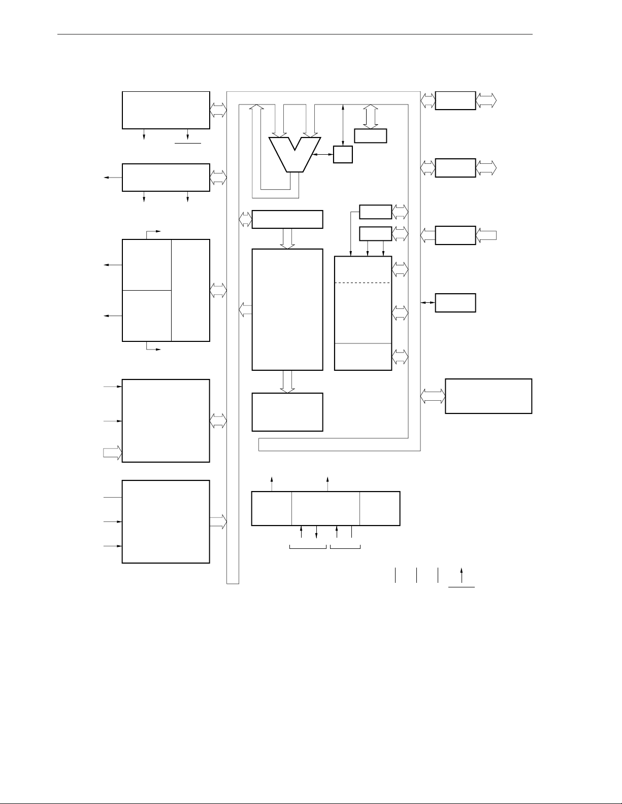
1.4 Block Diagram
CHAPTER 1 GENERAL
PTO0/P30
PTO1/P31
PTO2/P32
INT0/P61
KRREN
Basic interval
timer/watchdog timer
INTBT RESET
8-bit timer counter #0
INTT0 TOUT
INTT1
8-bit timer
counter #1
Cascaded
16-bit
timer
8-bit timer
counter
counter #2
INTT2
Interrupt control
ALU
Program counter
Program memory
(ROM)
4096 × 8 bits
Decode and
control
SP (8)
CY
SBS
Bank
General reg.
Data memory
(RAM)
128 × 4 bits
EEPROM
16 × 8 bits
Port 3 4
Port 6 4
Port 7 4
Port 8
P80
Bit seq. buffer (16)
P30 to P33
P60 to P63
P70 to P73
KR4/P70KR7/P73
REF
/P60
AV
PTH00/P62
PTH01/P63
4
φ
Standby
control
Programmable
f
Clock
divider
N
X
/2
CPU clock
System clock
generator
threshold port
CL1 CL2 X1 X2
In the case of
µ
PD754144
In the case of
µ
PD754244
IC V
DDVSS
RESET
20 User’s Manual U10676EJ3V0UM
Page 21
1.5 Pin Configuration (Top View)
• Pin configuration of µPD754144
• 20-pin plastic SOP (7.62 mm (300))
µ
PD754144GS-×××-BA5
• 20-pin plastic SSOP (7.62 mm (300))
µ
PD754144GS-×××-GJG
CHAPTER 1 GENERAL
RESET
CL1
CL2
V
IC
V
P60/AV
REF
P61/INT0
P62/PTH00
P63/PTH01
SS
DD
1
2
3
4
5
6
7
8
9
10
IC: Internally Connected (Directly connect to VDD.)
20
19
18
17
16
15
14
13
12
11
KRREN
P80
P30/PTO0
P31/PTO1
P32/PTO2
P33
P70/KR4
P71/KR5
P72/KR6
P73/KR7
User’s Manual U10676EJ3V0UM
21
Page 22
• Pin configuration of µPD754244
• 20-pin plastic SOP (7.62 mm (300))
µ
PD754244GS-×××-BA5
• 20-pin plastic SSOP (7.62 mm (300))
µ
PD754244GS-×××-GJG
CHAPTER 1 GENERAL
RESET
X1
X2
V
IC
V
P60/AV
REF
P61/INT0
P62/PTH00
P63/PTH01
SS
DD
1
2
3
4
5
6
7
8
9
10
IC: Internally Connected (Directly connect to V
DD.)
20
19
18
17
16
15
14
13
12
11
KRREN
P80
P30/PTO0
P31/PTO1
P32/PTO2
P33
P70/KR4
P71/KR5
P72/KR6
P73/KR7
22 User’s Manual U10676EJ3V0UM
Page 23

CHAPTER 1 GENERAL
Pin Name
P30 to P33: Port 3
P60 to P63: Port 6
P70 to P73: Port 7
P80: Port 8
KR4 to KR7: Key return 4 to 7
INT0: External vectored interrupt 0
PTH00, PTH01: Programmable threshold port analog input 0, 1
PTO0 to PTO2: Programmable timer output 0 to 2
KRREN: Key return reset enable
CL1, CL2: RC oscillator
X1, X2: Crystal/ceramic oscillator
IC: Internally connected
RESET: Reset
REF: Analog reference
AV
V
SS: Ground
VDD: Positive power supply
User’s Manual U10676EJ3V0UM
23
Page 24
2.1 Pin Functions of µPD754244
Table 2-1. Pin Functions of Digital I/O Ports
CHAPTER 2 PIN FUNCTIONS
Pin Name I/O
P30 I/O PTO0 × Input E-B
P31 PTO1
P32 PTO2
P33 –
P60 I/O AVREF × Input F -A
P61 INT0
P62 PTH00
P63 PTH01
P70 Input KR4 × Input B -A
P71 KR5
P72 KR6
P73 KR7
P80 I/O – × Input F -A
Alternate
Function I/O Type
Programmable 4-bit I/O port (Port 3).
Input/output can be specified in 1-bit units.
On-chip pull-up resistor can be specified by
software in 4-bit units.
Programmable 4-bit I/O port (Port 6).
Input/output can be specified in 1-bit units.
An on-chip pull-up resistor can be specified
by software in 4-bit units
A noise eliminator is selectable for P61/
INT0.
4-bit input port (Port 7).
A pull-up resistor can be incorporated (mask
option).
1-bit I/O port (PORT8).
An on-chip pull-up resistor can be specified
by software.
Function
Note 2
.
8-Bit
After Reset
I/O Circuit
Note 1
Notes 1. Circled characters indicate Schmitt-triggered input.
2. Do not specify connection of an on-chip pull-up resistor when using a programmable threshold port.
24 User’s Manual U10676EJ3V0UM
Page 25
CHAPTER 2 PIN FUNCTIONS
Table 2-2. Functions of Non-Port Pins
Pin Name I/O
Alternate
Function Type
Function
After Reset
I/O Circuit
Note
PTO0 Output P30 Timer counter output pins. Input E-B
PTO1 P31
PTO2 P32
INT0 Input P61 Edge-detected vectored interrupt input Input F -A
(edge to be detected is selectable).
Noise eliminator is selectable.
Noise
eliminator/
asynchronous
selectable
KR4 to KR7 Input P70 to P73 Falling edge-detected testable input. Input B -A
PTH00 Input P62 Variable threshold voltage 2-bit analog input. Input F -A
PTH01 P63
KRREN Input – Key return reset enable pin. Input B
Reset signal is generated at falling edge of KRn
when KRREN = high in STOP mode.
AVREF Input P60 Reference voltage input pin. Input F -A
CL1 Input – Provided in µPD754144 only. – –
These pins connect R and C for system clock
CL2 Output oscillation. No external clock can be input to
these pins.
X1 Input – Provided in µPD754244 only. – –
These pins connect crystal/ceramic oscillator for
X2 – system clock oscillation. When external clock is
used, input it to X1 and inverse phase to X2.
RESET Input – System reset input pin (active-low) – B -A
IC – – Internally connected. Connect directly to VDD.– –
VDD – – Positive power supply pin. – –
VSS – – Ground potential. – –
Note Circled characters indicate Schmitt triggered input.
User’s Manual U10676EJ3V0UM
25
Page 26

CHAPTER 2 PIN FUNCTIONS
2.2 Description of Pin Functions
2.2.1 P30 to P33 (Port 3) ... I/O pins shared with PTO0 to PTO2
P60 to P63 (Port 6) ... I/O pins shared with AV
P80 (Port 8) ... I/O pin
These are 4-bit I/O ports with output latches (ports 3 and 6) and a 1-bit I/O port with an output latch (port 8).
Ports 3 and 6 also have the following functions, in addition to the I/O port function.
• Port 3: Timer counter output (PTO0 to PTO2)
• Port 6: Programmable threshold port reference voltage input (AV
Vectored interrupt input (INT0)
Threshold variable voltage input (PTH00, PTH01)
The input or output mode of ports 3 and 6 is selected by port mode register group A (PMGA), and the input
or output mode of port 8 is selected by port mode register group C (PMGC). Ports 3 and 6 can be set to the input
or output mode in 1-bit units.
Ports 3, 6, and 8 can also be connected to an internal pull-up resistor by software. This is done by manipulating
the pull-up resistor specification registers (POGA and POGB). Specify connection of the pull-up resistor to ports
3 and 6 in 4-bit units. Connection of the pull-up resistor to port 8 can be specified in 1-bit units.
I/O for ports 3 and 6 is possible in 4-bit or 1-bit units. Manipulation in 8-bit units is not possible.
Generation of the RESET signal sets the input mode.
REF, INT0, PTH00, PTH01
REF)
2.2.2 P70 to P73 (Port 7) ... input pins shared with KR4 to KR7
Port 7 is a 4-bit input port.
This port also has a key interrupt input (KR4 to KR7) function, in addition the input port function.
Each pin is always set to input irrespective of the operation of alternate function pins. These pins have Schmitt-
triggered input to prevent malfunction due to noise.
Internal pull-up resistors are specifiable by a mask option in 1-bit units.
2.2.3 PTO0 to PTO2 ... output pins shared with port 3
These are the output pins of timer counters 0 to 2, and output square-wave pulses. To output the signal of a timer
counter, clear the output latch of the corresponding pin of port 3 to “0”. Then, set the bit corresponding to port 3 of
port mode register group A (PMGA) to “1” to set the output mode.
The output of the TOUT F/F pin is cleared to “0” by the timer start instruction.
For details, refer to 6.4.2 (3) Timer counter operation (8-bit).
26 User’s Manual U10676EJ3V0UM
Page 27

CHAPTER 2 PIN FUNCTIONS
2.2.4 INT0 ... input pin shared with port 6
This pin inputs the vectored interrupt signal detected by the edge. A noise eliminator is selectable for INT0. The
edge to be detected can be specified by using the edge detection mode register (IM0).
(1) INT0 (bits 0 and 1 of IM0)
(a) Active at rising edge
(b) Active at falling edge
(c) Active at both rising and falling edges
(d) External interrupt signal input disabled
INT0 is an asynchronous input pin, and a signal having a specific high-level width input to this pin can be
acknowledged as an interrupt, regardless of the operating clock of the CPU. In addition, an internal noise
eliminator can be connected to this pin by software, and the sampling clock that is used for noise elimination
can be changed in two steps. In this case, the width of the signal that can be acknowledged differs depending
on the CPU operating clock.
When the RESET signal is asserted, IM0 is cleared to “0”, and the rising edge is selected as the active edge.
INT0 can be used to release the STOP and HALT modes. However, when the noise eliminator is selected,
INT0 cannot be used to release the STOP and HALT modes.
INT0 is a Schmitt-triggered input pin.
2.2.5 KR4 to KR7 ... input pins shared with port 7
These are key interrupt input pins. KR4 to KR7 are parallel falling edge-detected interrupt input pins.
The interrupt source can be specified for “KR4 to KR7” by using the edge detection mode register (IM2).
When the RESET signal is asserted, these pins serve as port 7 pins and are set to the input mode.
2.2.6 KRREN
This is a key return reset function selection pin. It is always set to input.
When the KRREN pin is high and it is in STOP mode, a falling input on pins KR4/P70 to KR7/P73 generates a
system reset. At this time, STOP mode is released.
When the KRREN pin is low, pins KR4/P70 to KR7/P73 function as normal input pins or release standby.
2.2.7 TH00 and TH01 ... input pins shared with port 6
These are the input pins of the programmable threshold port (threshold voltage variable analog input port).
Setting the programmable threshold port mode register (PTHM) can change the threshold voltage in 16 stages.
User’s Manual U10676EJ3V0UM
27
Page 28
CHAPTER 2 PIN FUNCTIONS
2.2.8 AVREF ... input pin shared with port 6
This is a reference voltage input pin. An analog reference voltage for the programmable threshold port is input.
µ
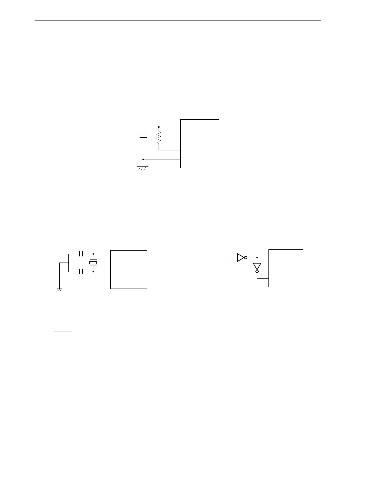
2.2.9 CL1 and CL2 (
PD754144 only)
These pins are used to connect the RC oscillator resistor (R) and capacitor (C) of the system clock oscillator.
No external clock can be input.
RC oscillation
µ
PD754144
CL1
C
R
CL2
VSS
2.2.10 X1 and X2 (µPD754244 only)
These pins connect a crystal/ceramic oscillator for system clock oscillation.
An external clock can also be input to these pins.
(a) Ceramic/crystal oscillation (b) External clock
PD754244
µ
X1
X2
Crystal resonator
or
ceramic resonator
µ
PD754244
X1
X2
SS
V
(4.194304 MHz TYP.)
ExternaI
clock
2.2.11 RESET
This pin inputs an active-low reset signal.
The RESET signal is an asynchronous input signal and is asserted when a signal with a specific low-level width
is input to this pin regardless of the operating clock. The RESET signal takes precedence over all the other operations.
This pin can not only be used to initialize and start the CPU, but also to release the STOP and HALT modes.
The RESET pin is a Schmitt-triggered input pin.
This pin can be connected to an internal pull-up resistor by a mask option.
28 User’s Manual U10676EJ3V0UM
Page 29
CHAPTER 2 PIN FUNCTIONS
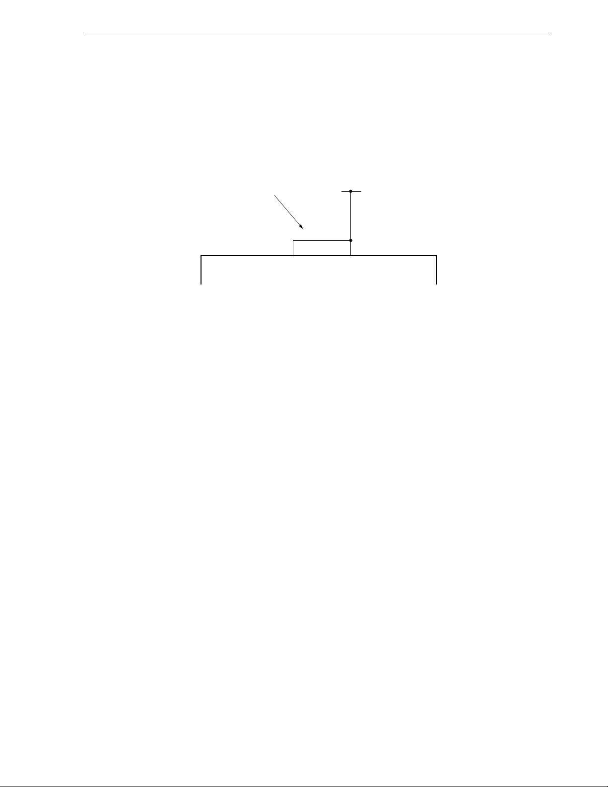
2.2.12 IC
The IC (Internally Connected) pin sets the test mode in which the µPD754244 is tested before shipment. Usually,
you should directly connect the IC pin to the V
If a voltage difference is generated between the IC and V
DD pin with as short a wiring length as possible.
DD pins because the wiring length is too long, or because
external noise is superimposed on the IC pin, your program may not be correctly executed.
2.2.13 VDD
Positive power supply pin.
2.2.14 V
SS
GND.
• Directly connect the IC pin to the V
Keep as short
as possible.
IC
V
DD
V
DD
DD pin.
User’s Manual U10676EJ3V0UM
29
Page 30
CHAPTER 2 PIN FUNCTIONS
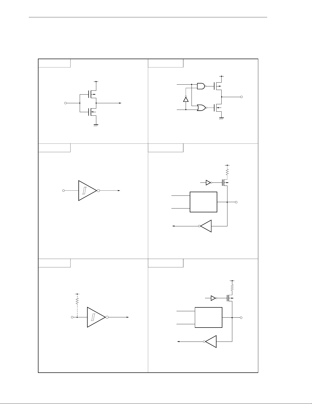
2.3 Pin I/O Circuits
The following diagrams show the I/O circuits of the pins of the µPD754244. Note that in these diagrams the I/
O circuits have been slightly simplified.
Type A
IN
CMOS specification input buffer.
Type B
IN
Type D
V
V
DD
Data
P-ch
N-ch
Output
disable
DD
P-ch
OUT
N-ch
Push-pull output that can be placed in output
high-impedance (both P-ch, N-ch off).
Type E-B
DD
V
P.U.R.
Data
Output
P.U.R.
enable
Type D
P-ch
IN/OUT
disable
Schmitt-triggered input with hysteresis characteristics.
Type B-A
DD
V
P.U.R (Mask Option)
IN
P.U.R. : Pull-Up Resistor
Type F-A
Output
disable
Data
Type A
P.U.R. : Pull-Up Resistor
P.U.R.
enable
Type D
Type B
P.U.R. : Pull-Up Resistor
V
DD
P.U.R.
P-ch
IN/OUT
30 User’s Manual U10676EJ3V0UM
Page 31

2.4 Processing of Unused Pins
Table 2-3. Recommended Connection of Unused Pins
Pin Recommended Connection
P30/PTO0 Input: Independently connect to VSS or VDD via a resistor.
P31/PTO1
P32/PTO2
P33
P60/AVREF
P61/INT0
P62/PTH00
P63/PTH01
P70/KR4 Connect to VDD.
P71/KR5
P72/KR6
CHAPTER 2 PIN FUNCTIONS
Output: Leave open.
P73/KR7
P80 Input: Independently connect to VSS or VDD via a resistor.
Output: Leave open.
KRREN When this pin is connected to VDD, the internal reset signal is
generated at the falling edge of the KRn pin in the STOP mode.
When this pin is connected to VSS, the internal reset signal is not
generated even if the falling edge of the KRn pin is detected in the
STOP mode.
IC Connect directly to VDD.
User’s Manual U10676EJ3V0UM
31
Page 32

CHAPTER 3 FEATURES OF ARCHITECTURE AND MEMORY MAP
The 75XL architecture employed for the µPD754244 has the following features.
• Internal RAM: 4K words × 4 bits MAX. (12-bit address)
• Expandability peripheral hardware
To realize these superb features, the following techniques have been employed.
(1) Bank configuration of data memory
(2) Bank configuration of general-purpose registers
(3) Memory mapped I/O
This chapter describes these features.
3.1 Bank Configuration of Data Memory and Addressing Modes
3.1.1 Bank configuration of data memory
The µPD754244 is provided with a static RAM at the addresses 000H to 07FH of memory bank 0 of the data memory
space. EEPROM (16 × 8 bits) is allocated to addresses 400H to 41FH of memory bank 4, and peripheral hardware
units (such as I/O ports and timers) are allocated to addresses F80H to FFFH of memory bank 15.
µ
PD754244 employs a memory bank configuration that directly or indirectly specifies the lower 8 bits of an
The
address by an instruction and the higher 4 bits of the address by a memory bank, to address the data memory space
of 12-bit address (4K words × 4 bits).
To specify a memory bank (MB), the following hardware units are provided.
• Memory bank enable flag (MBE)
• Memory bank select register (MBS)
MBS is a register that selects a memory bank. Memory banks 0, 4, and 15 can be set. MBE is a flag that enables
or disables the memory bank selected by MBS. When MBE is 0, the specified memory bank (MB) is fixed, regardless
of MBS, as shown in Figure 3-1. When MBE is 1, however, a memory bank is selected according to the setting of
MBS, so that the data memory space can be expanded.
To address the data memory space, MBE is usually set to 1 and the data memory of the memory bank specified
by MBS is manipulated. By selecting the mode of MBE = 0 or the mode of MBE = 1 for each processing of the program,
programming can be efficiently carried out.
Adapted Program Processing Effect
MBE = 0 mode • Interrupt servicing Saving/restoring MBS unnecessary
• Processing repeating internal hardware Changing MBS unnecessary
manipulation and stack RAM manipulation
• Subroutine processing Saving/restoring MBS unnecessary
MBE = 1 mode • Normal program processing
32 User’s Manual U10676EJ3V0UM
Page 33

CHAPTER 3 FEATURES OF ARCHITECTURE AND MEMORY MAP
Figure 3-1. Selecting MBE = 0 Mode and MBE = 1 Mode
<Main program>
SET 1 MBE
<Subroutine>
CLR1 MBE
RET
MBE = 0
(Interrupt servicing)
; MBE = 0 by vector table
MBE = 0
RETI
Internal hardware
and static RAM
manipulation
repeated.
MBE
= 1
CLR 1 MBE
MBE
= 0
SET 1 MBE
MBE
= 1
Remark Solid line: MBE = 1, dotted line: MBE = 0
Because MBE is automatically saved or restored during subroutine processing, it can be changed even while
subroutine processing is being executed. MBE can also be saved or restored automatically during interrupt servicing,
so that MBE during interrupt servicing can be specified as soon as the interrupt servicing is started, by setting the
interrupt vector table. This feature is useful for high-speed interrupt servicing.
To change MBS by using subroutine processing or interrupt servicing, save or restore it to the stack by using the
PUSH or POP instruction.
MBE is set by using the SET1 or CLR1 instruction. Use the SEL instruction to set MBS.
Examples 1. To clear MBE and fix memory bank
CLR1 MBE ; MBE ← 0
2. To select memory bank 4
SET1 MBE ; MBE ← 1
SEL MB4 ; MBE ← 4
User’s Manual U10676EJ3V0UM
33
Page 34

CHAPTER 3 FEATURES OF ARCHITECTURE AND MEMORY MAP
3.1.2 Addressing mode of data memory
The 75XL architecture employed for the µPD754244 provides the seven types of addressing modes shown in Table
3-1. This means that the data memory space can be efficiently addressed by the bit length of the data to be processed
and that programming can be carried out efficiently.
(1) 1-bit direct addressing (mem.bit)
This mode is used to directly address each bit of the entire data memory space by using the operand of an
instruction.
The memory bank (MB) to be specified is fixed to 0 in the mode of MBE = 0 if the address specified by the
operand ranges from 00H to 7FH, and to 15 if the address specified by the operand is 80H to FFH. In the
mode of MBE = 0, therefore, both the data area of addresses 000H to 07FH and the peripheral hardware area
of F80H to FFFH can be addressed.
In the mode of MBE = 1, MB = MBS; therefore, the entire data memory space can be addressed.
This addressing mode can be used with four instructions: the bit set and reset instructions (SET1 and CLR1),
and the two bit test (SKT and SKF).
Example To set FLAG1, reset FLAG2, and test whether FLAG3 is 0
FLAG1 EQU 03FH.1 ; Bit 1 of address 3FH
FLAG2 EQU 057H.2 ; Bit 2 of address 57H
FLAG3 EQU 077H.0 ; Bit 0 of address 77H
SET1 MBE ; MBE ← 1
SEL MB0 ; MBS ← 0
SET1 FLAG1 ; FLAG1 ← 1
CLR1 FLAG2 ; FLAG2 ← 0
SKF FLAG3 ; FLAG3 = 0?
34 User’s Manual U10676EJ3V0UM
Page 35

CHAPTER 3 FEATURES OF ARCHITECTURE AND MEMORY MAP
Figure 3-2. Data Memory Configuration and Addressing Range for Each Addressing Mode
Addressing mode
mem
mem. bit
@HL
@H+mem. bit
@DE
@DL
Stack
addressing
fmem. bit
pmem. @L
Memory bank enable flag MBE = 0 MBE = 1 MBE = 0 MBE = 1 ––––
000H
01FH
020H
07FH
Data area (SRAM)
Generalpurpose
register area
MBS = 0 MBS = 0 SBS = 0
Memory bank 0
Not
incorporated
0FFH
400H
41FH
Data area
(EEPROM16 × 8)
MBS = 4 MBS = 4
Memory bank 4
Not
incorporated
4FFH
F80H
FB0H
FBFH
FC0H
Peripheral
hardware area
(memory bank 15)
MBS =
15
MBS =
15
FF0H
FFFH
Remark – : don’t care
Caution EEPROM can be manipulated by the following 8-bit manipulation instructions only.
MOV XA, @HL XCH XA, @HL
MOV XA, mem XCH XA, mem
MOV @HL, XA SKE XA, @HL
MOV mem, XA
User’s Manual U10676EJ3V0UM
35
Page 36
CHAPTER 3 FEATURES OF ARCHITECTURE AND MEMORY MAP
Table 3-1. Addressing Modes
Addressing Mode Representation Specified Address
• When MBE = 0
When mem = 00H to 7FH: MB = 0
When mem = 80H to FFH: MB = 15
• When MBE = 1: MB = MBS
4-bit direct addressing mem Address specified by MB and mem.
• When MBE = 0
When mem = 00H to 7FH: MB = 0
When mem = 80H to FFH: MB = 15
• When MBE = 1: MB = MBS
8-bit direct addressing Address specified by MB and mem (mem is even address)
• When MBE = 0
When mem = 00H to 7FH: MB = 0
When mem = 80H to FFH: MB = 15
• When MBE = 1: MB = MBS
4-bit register indirect @HL Address specified by MB and HL.
addressing Where, MB = MBE MBS
@HL+ Address specified by MB and HL. However, MB = MBE
@HL– HL+ automatically increments L register after addressing.
.
MBS.
.
HL– automatically decrements L register after addressing.
@DE Address specified by DE in memory bank 0
@DL Address specified by DL in memory bank 0
8-bit register indirect @HL Address specified by MB and HL (contents of L register are even
addressing number)
Where, MB = MBE MBS
Bit manipulation fmem.bit Bit specified by bit at address specified by fmem
.
addressing fmem = FB0H to FBFH (interrupt-related hardware)
FF0H to FFFH (I/O port)
pmem.@L Bit specified by lower 2 bits of L register at address specified by
higher 10 bits of pmem and lower 2 bits of L register.
Where, pmem = FC0H to FFFH
@H+mem.bit Bit specified by bit at address specified by MB, H, and lower 4 bits
of mem.
Where, MB = MBE MBS
Stack addressing — Address specified by SP in memory bank 0
.
36 User’s Manual U10676EJ3V0UM
Page 37

CHAPTER 3 FEATURES OF ARCHITECTURE AND MEMORY MAP
(2) 4-bit direct addressing (mem)
This addressing mode is used to directly address the entire memory space in 4-bit units by using the operand
of an instruction.
Like the 1-bit direct addressing mode, the area that can be addressed is fixed to the data area of addresses
000H to 07FH and the peripheral hardware area of F80H to FFFH in the mode of MBE = 0. In the mode of
MBE = 1, MB = MBS, and the entire data memory space can be addressed.
This addressing mode is applicable to the MOV, XCH, INCS, IN, and OUT instructions.
(3) 8-bit direct addressing (mem)
This addressing mode is used to directly address the entire data memory space in 8-bit units by using the
operand of an instruction.
The address that can be specified by the operand is an even address. The 4-bit data of the address specified
by the operand and the 4-bit data of the address higher than the specified address are used in pairs and
processed in 8-bit units by the 8-bit accumulator (XA register pair).
The memory bank that is addressed is the same as that addressed in the 4-bit direct addressing mode.
This addressing mode is applicable to the MOV, XCH, IN, and OUT instructions.
(4) 4-bit register indirect addressing (@rpa)
This addressing mode is used to indirectly address the data memory space in 4-bit units by using a data pointer
(a pair of general-purpose registers) specified by the operand of an instruction.
As the data pointer, three register pairs can be specified: HL that can address the entire data memory space
by using MBE and MBS, and DE and DL that always address memory bank 0, regardless of the specification
by MBE and MBS. The user selects a register pair depending on the data memory bank to be used in order
to carry out programming efficiently.
When register HL is specified, auto increment/decrement mode can be used. This mode is used to increment
or decrement register L automatically by 1 at the same time as each instruction is executed, therefore it can
reduce the number of program steps.
Example To transfer data 50H to 57H to addresses 60H to 67H
DATA1 EQU 57H
DATA2 EQU 67H
SET1 MBE
SEL MB0
MOV D, #DATA1 SHR4
MOV HL, #DATA2 AND 0FFH ; HL ← 17H
LOOP : MOV A, @DL ; A ← (DL)
XCH A, @HL ; A ← (HL)
DECS L ; L ← L – 1
BR LOOP
The addressing mode that uses register pair HL as the data pointer is widely used to transfer, operate, compare,
and input/output data. The addressing mode using register pair DE or DL is used with the MOV and XCH instructions.
By using this addressing mode in combination with the increment/decrement instruction of a general-purpose
register or a register pair, the addresses of the data memory can be updated as shown in Figure 3-3.
User’s Manual U10676EJ3V0UM
37
Page 38

CHAPTER 3 FEATURES OF ARCHITECTURE AND MEMORY MAP
Examples 1. To compare data 50H to 57H with data 60H to 67H
DATA1 EQU 57H
DATA2 EQU 67H
SET1 MBE
SEL MB0
MOV D, #DATA1 SHR 4
MOV HL, #DATA2 AND 0FFH
LOOP : MOV A, @DL
SKE A, @HL ; A = (HL)?
BR NO ; NO
DECS L ; YES, L ← L – 1
BR LOOP
2. To clear data memory of 004H to 07FH
CLR1 RBE
CLR1 MBE
MOV XA, #00H
MOV HL, #04H
LOOP : MOV @HL, A ; (HL) ← A
INCS L ; L ← L+1
BR LOOP
INCS H ; H ← H+1
NOP
SKE H, #08H
BR LOOP
38 User’s Manual U10676EJ3V0UM
Page 39

CHAPTER 3 FEATURES OF ARCHITECTURE AND MEMORY MAP
Figure 3-3. Updating Address of Static RAM
0XH
X0H
DECS D
@DL
DECS L INCS L
Auto
decrement
DECS L INCS L
DECS HL INCS HL
4-bit
transfer
INCS D
DECS H
@HL 4-bit
manipulation
8-bit
manipuIation
INCS H
Auto
increment
DECS DE INCS DE
Direct addressing
bit manipulation
4-bit transfer
8-bit transfer
DECS D
DECS E INCS E
@DE
4-bit
transfer
INCS D
DECS H
@H+mem.
bit
manipulation
INCS H
XFH
FXH
User’s Manual U10676EJ3V0UM
39
Page 40

CHAPTER 3 FEATURES OF ARCHITECTURE AND MEMORY MAP
(5) 8-bit register indirect addressing (@HL)
This addressing mode is used to indirectly address the entire data memory space in 8-bit units by using a data
pointer (HL register pair).
In this addressing mode, data is processed in 8-bit units, that is, the 4-bit data at an address specified by the
data pointer with bit 0 (bit 0 of the L register) cleared to 0 and the 4-bit data at the address higher are used
in pairs and processed with the data of the 8-bit accumulator (XA register).
The memory bank is specified in the same manner as when the HL register is specified in the 4-bit register
indirect addressing mode, by using MBE and MBS. This addressing mode is applicable to the MOV, XCH,
and SKE instructions.
Examples 1. To compare whether the count register (T0) value of timer counter 0 is equal to the data at addresses
30H and 31H
DATA EQU 30H
CLR1 MBE
MOV HL, #DATA
MOV XA, T0 ; XA ← count register 0
SKE XA, @HL ; XA = (HL)?
2. To clear data memory at 004H to 07FH
CLR1 RBE
CLR1 MBE
MOV XA, #00H
MOV HL, #04H
LOOP : MOV @HL, XA ; (HL) ← XA
INCS L
INCS L
BR LOOP
INCS H
NOP
SKE H, #08H
BR LOOP
40 User’s Manual U10676EJ3V0UM
Page 41

CHAPTER 3 FEATURES OF ARCHITECTURE AND MEMORY MAP
(6) Bit manipulation addressing
This addressing mode is used to manipulate the entire memory space in bit units (such as Boolean processing
and bit transfer).
While the 1-bit direct addressing mode can only be used with the instructions that set, reset, or test a bit, this
addressing mode can be used in various ways such as Boolean processing by the AND1, OR1, and XOR1
instructions, and test and reset by the SKTCLR instruction.
Bit manipulation addressing can be implemented in the following three ways, which can be selected depending
on the data memory address to be used.
(a) Specific address bit direct addressing (fmem.bit)
This addressing mode is to manipulate the hardware units that use bit manipulation especially often, such
as I/O ports and interrupt-related flags, regardless of the setting of the memory bank. Therefore, the data
memory addresses to which this addressing mode is applicable are FF0H to FFFH, to which the I/O ports
are mapped, and FB0H to FBFH, to which the interrupt-related hardware units are mapped. The hardware
units in these two data memory areas can be manipulated in bit units at any time in the direct addressing
mode, regardless of the setting of MBS and MBE.
Examples 1. To test the timer 0 interrupt request flag (IRQT0) and, if it is set, clear the flag and reset P63
SKTCLR IRQT0 ; IRQT0 = 1?
BR NO ; NO
CLR1 PORT6.3 ; YES
2. To reset P63 if both P30 and P71 pins are 1
P30
P71
P63
(i) SET1 CY ; CY ← 1
AND1 CY, PORT3.0 ; CY
P30
AND1 CY, PORT7.1 ; CY P71
SKT CY ; CY = 1?
BR SETP
CLR1 PORT6.3 ; P63 ← 0
•
•
•
SETP : SET1 PORT6.3 ; P63 ← 1
•
•
•
(ii) SKT PORT3.0 ; P30 = 1?
BR SETP
SKT PORT7.1 ; P71 = 1?
BR SETP
CLR1 PORT6.3 ; P63 ← 0
•
•
•
SETP: SET1 PORT6.3 ; P63 ← 1
User’s Manual U10676EJ3V0UM
41
Page 42

CHAPTER 3 FEATURES OF ARCHITECTURE AND MEMORY MAP
(b) Specific address bit register indirect addressing (pmem, @L)
This addressing mode is to indirectly specify and successively manipulate the bits of the peripheral
hardware units such as I/O ports. The data memory addresses to which this addressing mode can be
applied are FC0H to FFFH.
This addressing mode specifies the higher 10 bits of a 12-bit data memory address directly by using an
operand, and the lower 2 bits by using the L register.
This addressing mode can also be used independently of the setting of MBE and MBS.
Example To output pulses to the respective bits of port 6
P60
P61
P62
P63
LOOP2 : MOV L, #0
LOOP1 : SET1 PORT6.@L; Bits of port 6 (L1-0) ← 1
CLR1 PORT6.@L; Bits of port 6 (L1-0) ← 0
INCS L
SKE L, #4H
BR LOOP1
BR LOOP2
42 User’s Manual U10676EJ3V0UM
Page 43

CHAPTER 3 FEATURES OF ARCHITECTURE AND MEMORY MAP
(c) Special 1-bit direct addressing (@H+mem.bit)
This addressing mode enables bit manipulation in the entire memory space.
The higher 4 bits of the data memory address of the memory bank specified by MBE and MBS are indirectly
specified by the H register, and the lower 4 bits and the bit address are directly specified by the operand.
This addressing mode can be used to manipulate the respective bits of the entire data memory area in
various ways.
Example To reset bit 2 (FLAG3) at address 32H if both bit 3 (FLAG1) at address 30H and bit 0 (FLAG2) at address
31H are 0 or 1
FLAG1 EQU 30H.3
FLAG2 EQU 31H.0
FLAG3 EQU 32H.2
SEL MB0
MOV H, #FLAG1 SHR 6
CLR1 CY ; CY ← 0
OR1 CY, @H+FLAG1 ; CY ← CY
XOR1 CY, @H+FLAG2 ; CY ← CY FLAG2
SET1 @H+FLAG3 ; FLAG3 ← 1
SKT CY ; CY = 1?
CLR1 @H+FLAG3 ; FLAG3 ← 0
FLAG1
FLAG2
FLAG3
FLAG1
User’s Manual U10676EJ3V0UM
43
Page 44

CHAPTER 3 FEATURES OF ARCHITECTURE AND MEMORY MAP
(7) Stack addressing
This addressing mode is used to save or restore data when interrupt servicing or subroutine processing is
executed.
The address of data memory bank 0 pointed to by the stack pointer (8 bits) is specified in this addressing mode.
In addition to being used during interrupt servicing or subroutine processing, this addressing is also used to
save or restore register contents by using the PUSH or POP instruction.
Examples 1. To save or restore register contents during subroutine processing
SUB : PUSH XA
PUSH HL
PUSH BS ; Saves MBS and RBS
•
•
•
POP BS
POP HL
POP XA
RET
2. To transfer contents of register pair HL to register pair DE
PUSH HL
POP DE ; DE ← HL
3. To branch to address specified by registers [XABC]
PUSH BC
PUSH XA
RET ; To branch address XABC
44 User’s Manual U10676EJ3V0UM
Page 45

CHAPTER 3 FEATURES OF ARCHITECTURE AND MEMORY MAP
3.2 Bank Configuration of General-Purpose Registers
The µPD754244 is provided with four register banks with each bank consisting of eight general-purpose registers:
X, A, B, C, D, E, H, and L. The general-purpose register area consisting of these registers is mapped to the addresses
00H to 1FH of memory bank 0 (refer to Figure 3-5 Configuration of General-Purpose Registers (4-Bit Process-
ing)). To specify a general-purpose register bank, a register bank enable flag (RBE) and a register bank select register
(RBS) are provided. RBS selects a register bank, and RBE determines whether the register bank selected by RBS
is valid or not. The register bank (RB) that is enabled when an instruction is executed is as follows:
.
RB = RBE
RBS
Table 3-2. Register Bank Selected by RBE and RBS
RBE Register Bank
3210
000××Fixed to bank 0
1 0000Bank 0 selected
0 1 Bank 1 selected
1 0 Bank 2 selected
1 1 Bank 3 selected
Fixed to 0
Remark × = don’t care
RBE is automatically saved or restored during subroutine processing and therefore can be set while subroutine
processing is under execution. When interrupt servicing is executed, RBE is automatically saved or restored, and
RBE can be set during interrupt servicing depending on the setting of the interrupt vector table as soon as the interrupt
servicing is started. Consequently, if different register banks are used for normal processing and interrupt servicing
as shown in Table 3-3, it is not necessary to save or restore general-purpose registers when an interrupt is serviced,
and only RBS needs to be saved or restored if two interrupts are nested. This means that the interrupt servicing speed
can be increased.
RBS
Table 3-3. Example of Using Different Register Banks for Normal Routine and Interrupt Routine
Normal processing Uses register bank 2 or 3 with RBE = 1
Single interrupt servicing Uses register bank 0 with RBE = 0
Nesting servicing of two Uses register bank 1 with RBE = 1
interrupts (at this time, RBS must be saved or restored)
Nesting servicing of Registers must be saved or restored by PUSH or POP instructions
three or more interrupts
User’s Manual U10676EJ3V0UM
45
Page 46

CHAPTER 3 FEATURES OF ARCHITECTURE AND MEMORY MAP
<Main program>
SET1 RBE
SEL RB2
Figure 3-4. Example of Using Register Banks
<Single interrupt> <Nesting of two
; RBE = 0
in vector table
interrupts> ; RBE = 1
in vector table
<Nesting of three
interrupts> ; RBE = 0
in vector table
RB = 2
RB = 0
PUSH BS
SEL
RB = 1
RETI POP BS
RETI
RB1
RB = 0
PUSH rp
POP rp
RETI
If RBS is to be changed in the course of subroutine processing or interrupt servicing, it must be saved or restored
by using the PUSH or POP instruction.
RBE is set by using the SET1 or CLR1 instruction. RBS is set by using the SEL instruction.
Example SET1 RBE ; RBE ← 1
CLR1 RBE ; RBE ← 0
SEL RB0 ; RBS ← 0
SEL RB3 ; RBS ← 3
µ
The general-purpose register area provided in the
PD754244 can be used not only as 4-bit registers but also
as 8-bit register pairs. This feature allows the µPD754244 to provide transfer, operation, comparison, and increment/
decrement instructions comparable to those of 8-bit microcontrollers and allows you to program using mainly general-
purpose registers.
46 User’s Manual U10676EJ3V0UM
Page 47

CHAPTER 3 FEATURES OF ARCHITECTURE AND MEMORY MAP
(1) To use as 4-bit registers
When the general-purpose register area is used as a 4-bit register area, a total of eight general-purpose
registers, X, A, B, C, D, E, H, and L, specified by RBE and RBS can be used as shown in Figure 3-5. Of these
registers, A plays a central role in transferring, operating, and comparing 4-bit data as a 4-bit accumulator.
The other registers can transfer, compare, and increment or decrement data with the accumulator.
(2) To use as 8-bit registers
When the general-purpose register area is used as an 8-bit register area, a total of eight 8-bit register pairs
can be used as shown in Figure 3-6: register pairs XA, BC, DE, and HL of a register bank specified by RBE
and RBS, and register pairs XA’, BC’, DE’, and HL’ of the register bank whose bit 0 is complemented in respect
to the register bank (RB). Of these register pairs, XA serves as an 8-bit accumulator, playing the central role
in transferring, operating, and comparing 8-bit data. The other register pairs can transfer, compare, and
increment or decrement data with the accumulator. The HL register pair is mainly used as a data pointer.
The DE and DL register pairs are also used as auxiliary data pointers.
Examples 1. INCS HL ; Skips if HL ← HL+1, HL=00H
ADDS XA, BC ; Skips if XA ← XA+BC and carry occurs
SUBC DE’, XA ; DE’ ← DE’ – XA – CY
MOV XA, XA’ ; XA ← XA’
MOVT XA, @PCDE ; XA ← (PC
11–8+DE) ROM, table reference
SKE XA, BC ; Skips if XA = BC
2. To test whether the value of the count register (T0) of timer counter 0 is greater than the value
of register pair BC’ and, if not, to wait until it becomes greater
CLR1 MBE
NO : MOV XA, T0 ; Reads count register
SUBS XA, BC’ ; XA ≥ BC’ ?
BR YES ; YES
BR NO ; NO
User’s Manual U10676EJ3V0UM
47
Page 48

CHAPTER 3 FEATURES OF ARCHITECTURE AND MEMORY MAP
Figure 3-5. Configuration of General-Purpose Registers (4-Bit Processing)
X
01H
H
03H
D
05H
B
07H
X
09H
H
0BH
D
0DH
B
0FH
X
11H
H
13H
D
15H
A
L
E
C
A
L
E
C
A
L
E
00H
02H
04H
06H
08H
0AH
0CH
0EH
10H
12H
14H
Register bank 0
.
(RBE RBS = 0)
Register bank 1
.
(RBE RBS = 1)
Register bank 2
.
(RBE RBS = 2)
B
17H
X
19H
H
1BH
D
1DH
B
1FH
C
A
L
E
C
16H
18H
1AH
1CH
1EH
Register bank 3
.
(RBE RBS = 3)
48 User’s Manual U10676EJ3V0UM
Page 49
CHAPTER 3 FEATURES OF ARCHITECTURE AND MEMORY MAP
Figure 3-6. Configuration of General-Purpose Registers (8-Bit Processing)
XA
HL
DE
BC
XA'
HL'
DE'
BC'
XA
00H
02H
04H
06H
08H
0AH
0CH
0EH
10H
When
.
RBE RBS = 0
XA'
HL'
DE'
BC'
XA
HL
DE
BC
XA'
00H
02H
04H
06H
08H
0AH
0CH
0EH
10H
When
.
RBE RBS = 1
HL
DE
BC
XA'
HL'
DE'
BC'
12H
14H
16H
18H
1AH
1CH
1EH
HL'
DE'
BC'
When
..
RBE RBS = 2
XA
HL
DE
BC
12H
14H
16H
18H
1AH
1CH
1EH
When
RBE RBS = 3
User’s Manual U10676EJ3V0UM
49
Page 50

CHAPTER 3 FEATURES OF ARCHITECTURE AND MEMORY MAP
3.3 Memory-Mapped I/O
The µPD754244 employs memory-mapped I/O that maps peripheral hardware units such as I/O ports and timers
to addresses F80H to FFFH on the data memory space, as shown in Figure 3-2. Therefore, no special instructions
to control the peripheral hardware units are provided, and all the hardware units are controlled by using memory
manipulation instructions. (Some mnemonics that make the program easy to read are provided for hardware control.)
To manipulate peripheral hardware units, the addressing modes shown in Table 3-4 can be used.
Table 3-4. Addressing Modes Applicable to Peripheral Hardware Unit Manipulation
Applicable Addressing Mode Hardware Units
Bit manipulation Specified in direct addressing mode mem.bit with All hardware units that can be
MBE = 0 or (MBE = 1, MBS = 15) manipulated in 1-bit units
Specified in direct addressing mode fmem.bit regardless IST1, IST0, MBE, RBE
of setting of MBE and MBS IE×××, IRQ×××, PORTn.×
Specified in indirect addressing mode pmem.@L BSBn.×
regardless of setting of MBE and MBS PORTn.×
4-bit manipulation
8-bit manipulation Specified in direct addressing mem with MBE = 0 or All hardware units that can be
Example CLR1 MBE ; MBE = 0
Specifies in direct addressing mode mem with
or (MBE = 1
Specified in register indirect addressing @HL with
(MBE = 1, MBS = 15)
(MBE = 1, MBS = 15), where mem is even number. manipulated in 8-bit units
Specified in register indirect addressing @HL with
MBE = 1, MBS = 15, where contents of L register
are even number
SET1 TM0. 3 ; Starts timer 0
EI IE0 ; Enables INT0
DI IET1 ; Disables INTT1
SKTCLR IRQ2 ; Tests and clears INT2 request flag
SET1 PORT3, @L ; Sets port 3
IN A, PORT6 ; A ← port 6
, MBS = 15) manipulated in 4-bit units
MBE = 0 All hardware units that can be
50 User’s Manual U10676EJ3V0UM
Page 51

CHAPTER 3 FEATURES OF ARCHITECTURE AND MEMORY MAP
Figure 3-7 shows the I/O map of the µPD754244.
The meanings of the symbols shown in this figure are as follows.
• Symbol ............ Name indicating the address of an internal hardware unit
Can be written in operands of instructions
• R/W ................. Indicates whether the hardware unit in question can be read or written
R/W: Read/write
R: Read only
W: Write only
• Number of bits that can be manipulated .......... Indicates the bit units in which the hardware unit in question can
be manipulated
: Can be manipulated in specified units (1, 4, or 8 bits)
: Only some bits can be manipulated. For the bits that can be
manipulated, refer to Remarks.
– : Cannot be manipulated in specified units (1, 4, or 8 bits).
• Bit manipulation addressing ............................... Indicates a bit manipulation addressing mode that can be used to
manipulate the hardware unit in question in 1-bit units
User’s Manual U10676EJ3V0UM
51
Page 52

CHAPTER 3 FEATURES OF ARCHITECTURE AND MEMORY MAP
Figure 3-7. µPD754244 I/O Map (1/8)
Address R/W
F80H Stack pointer (SP) R/W – –
F82H
................................................................................
................................................................................
F83H
F84H Stack bank selection register (SBS) R/W – ––
F85H Basic interval timer mode register (BTM) W
F86H Basic interval timer (BT) R – – –
F88H Modulo register for setting timer counter 2 R/W – –
F8AH Unmounted
F8BH
F8CH Unmounted
to
F8FH
Hardware name (symbol)
b3 b2 b1 b0 1-bit 4-bit 8-bit
Register bank selection register (RBS)
Bank selection register (BS) R
Memory bank selection register (MBS)
high-level period (TMOD2H)
Note 2
WDTM
–––W – – mem.bit
Number of bits that
can be manipulated
–
–
– mem.bit
Bit
manipulation Remarks
addressing
– Bit 0 is fixed to 0.
– Note 1
–
Bit manipulation can be performed only on bit 3.
Notes 1. Manipulation is possible separately with RBS and MBS in 4-bit manipulation. Manipulation is possible
with BS in 8-bit manipulation. Write data into MBS and RBS with the SEL MBn (n = 0, 4 or 15) and
SEL RBn (n = 0-3) instructions.
2. WDTM: Watchdog timer enable flag (W); Once set, cannot be cleared by an instruction.
52 User’s Manual U10676EJ3V0UM
Page 53
CHAPTER 3 FEATURES OF ARCHITECTURE AND MEMORY MAP
Figure 3-7. µPD754244 I/O Map (2/8)
Address R/W
F90H Timer counter 2 mode register (TM2) R/W
F92H
................................................................................
................................................................................
F94H Timer counter 2 count register (T2) R ––
F96H Timer counter 2 modulo register (TMOD2) R/W ––
F98H Unmounted
to
F9FH
Hardware name (symbol)
b3 b2 b1 b0 1-bit 4-bit 8-bit
TOE2 REMC NRZB NRZ
Timer counter 2 control register (TC2)
0 –––
Number of bits that
can be manipulated
(W) – –
–– –
R/W
–– Only 0 can be written to bit 3
Bit
manipulation Remarks
addressing
Bit manipulation can be performed only on bit 3
– Bit 3 can only be written
–
–
User’s Manual U10676EJ3V0UM
53
Page 54
CHAPTER 3 FEATURES OF ARCHITECTURE AND MEMORY MAP
Figure 3-7. µPD754244 I/O Map (3/8)
Address R/W
FA0H Timer counter 0 mode register (TM0) R/W
FA2H
FA3H Unmounted
FA4H Timer counter 0 count register (T0) R ––
FA6H Timer counter 0 modulo register (TMOD0) R/W ––
FA8H Timer counter 1 mode register (TM1) R/W
FAAH
FABH Unmounted
FACH Timer counter 1 count register (T1) R ––
Hardware name (symbol)
b3 b2 b1 b0 1-bit 4-bit 8-bit
Note 1
TOE0
TOE1
Note 2
–––W –– mem.bit
–––W –– mem.bit
Number of bits that
can be manipulated
(W) – mem.bit
–– –
(W) – mem.bit
–– –
Bit
manipulation Remarks
addressing
Bit manipulation can be performed only on bit 3
–
–
Bit manipulation can be performed only on bit 3
–
FAEH Timer counter 1 modulo register (TMOD1) R/W ––
Notes 1. TOE0: Timer counter output enable flag (channel 0) (W)
2. TOE1: Timer counter output enable flag (channel 1) (W)
–
54 User’s Manual U10676EJ3V0UM
Page 55

CHAPTER 3 FEATURES OF ARCHITECTURE AND MEMORY MAP
Figure 3-7. µPD754244 I/O Map (4/8)
Address R/W
FB0H
................................................................................
................................................................................
FB2H Interrupt priority selection register (IPS) R/W –
FB3H Processor clock control register (PCC) R/W –
FB4H INT0 edge detection mode register (IM0) R/W –
FB5H Unmounted
FB6H INT2 edge detection mode register (IM2)
FB7H Unmounted
................................................................................
FB8H R/W
................................................................................
FB9H R/W
FBAH Unmounted
FBBH
................................................................................
FBCH R/W
................................................................................
FBDH R/W
................................................................................
FBEH R/W
................................................................................
FBFH R/W
Hardware name (symbol)
b3 b2 b1 b0 1-bit 4-bit 8-bit
IST1 IST0 MBE RBE
Program status word (PSW)
Note 1
CY
INTA register (INTA)
––IEBT IRQBT
INTB register (INTB)
IEEE IRQEE ––
INTE register (INTE)
IET1 IRQT1 IET0 IRQT0
INTF register (INTF)
IET2 IRQT2 ––
INTG register (INTG)
––IE0 IRQ0
INTH register (INTH)
––IE2 IRQ2
SK2
Note 1
SK1
Note 1
SK0
R/W
Note 1
Note 5
R/W – ––
Number of bits that
can be manipulated
(R/W) (R/W)
Note 2
(R) fmem.bit R only possible as 8-bit manipulation.
–
– Note 3
– Note 4
––
– fmem.bit Bit manipulation can be performed by
–
– fmem.bit Bit manipulation can be performed by
–
–
–
Bit
manipulation Remarks
addressing
reserved word only.
reserved word only.
Remarks 1. IE××× is an interrupt enable flag.
2. IRQ××× is an interrupt request flag.
Notes 1. These are not registered as reserved words.
2. Use the CY manipulation instruction to write to CY.
3. IME (bit 3) can only be manipulated by an EI/DI instruction.
4. PCC3 (bit 3) and PCC2 (bit 2) can be manipulated by a STOP/HALT instruction.
5. This register specifies the falling edge of the KRn pin as the set signal of the interrupt request flag
(IRQ2). This register is initialized to 00H after reset. Therefore, write 01H to set the falling edge of
the KRn pin to IRQ2.
User’s Manual U10676EJ3V0UM
55
Page 56
CHAPTER 3 FEATURES OF ARCHITECTURE AND MEMORY MAP
Figure 3-7. µPD754244 I/O Map (5/8)
Address R/W
Hardware name (symbol)
b3 b2 b1 b0 1-bit 4-bit 8-bit
FC0H Bit sequential buffer 0 (BSB0) R/W
FC1H Bit sequential buffer 1 (BSB1) R/W
Number of bits that
can be manipulated
Bit
manipulation Remarks
addressing
mem.bit
pmem.@L
FC2H Bit sequential buffer 2 (BSB2) R/W
FC3H Bit sequential buffer 3 (BSB3) R/W
FC4H Unmounted
FC5H
Reset detection flag register (RDF)
................................................................................
FC6H
KRF WDF ––
R/W
– mem.bit
FC7H Unmounted
to
FCDH
Note 1
FCEH R/W
EWE
................................................................................
EEPROM write control register (EWC) the read value is undefined.
................................................................................
FCFH
ERE
Note 1
EWST
EWTC6
Note 1
Note 2
––
Note 2
EWTC5
EWTC4
Note 2
– mem.bit A write to an unmounted area is invalid, and
–
Notes 1. In bit manipulation: EWE = R/W, EWST = R only, ERE = R/W.
2. These are not registered as reserved words.
Manipulation can be performed only on bits 2 and 3.
56 User’s Manual U10676EJ3V0UM
Page 57
CHAPTER 3 FEATURES OF ARCHITECTURE AND MEMORY MAP
Figure 3-7. µPD754244 I/O Map (6/8)
Address R/W
Hardware name (symbol)
Number of bits that
can be manipulated
b3 b2 b1 b0 1-bit 4-bit 8-bit
FD0H Unmounted
to
FD3H
FD4H Programmable threshold port (PTH0) R
FD5H Unmounted
Note
PTHM3
FD6H R/W ––
................................................................................
Programmable threshold port mode register (PTHM)
................................................................................
Note
PTHM7
PTHM2
PTHM6
Note
PTHM1
Note
––
Note
PTHM0
Note
FD8H Unmounted
to
FDBH
Note
FDCH
FDEH
PO3
................................................................................
Pull-up resistor specification register group A (POGA)
....................................................................
–
–––PO8
................................................................................
Pull-up resistor specification register group B (POGB)
................................................................................
––––
–––
PO6
Note
––
Note
R/W ––
R/W –– –
Note These are not registered as reserved words.
Bit
manipulation Remarks
addressing
– mem.bit
mem.bit A write to bit 4 or bit 5 is invalid, and the read
value is undefined.
– A write to an unmounted area is invalid, and
the read value is undefined.
User’s Manual U10676EJ3V0UM
57
Page 58

CHAPTER 3 FEATURES OF ARCHITECTURE AND MEMORY MAP
Figure 3-7. µPD754244 I/O Map (7/8)
Address R/W
Hardware name (symbol)
Number of bits that
can be manipulated
b3 b2 b1 b0 1-bit 4-bit 8-bit
FE0H Unmounted
to
FE7H
FE8H
PM33 PM32 PM31 PM30
................................................................................
Port mode register group A (PMGA)
................................................................................
PM63
Note
PM62
Note
PM61
Note
PM60
Note
R/W
FEAH Unmounted
to
FEDH
FEEH
–––PM8
................................................................................
Port mode register group C (PMGC) the read value is undefined.
................................................................................
––––
Note
R/W –– – A write to an unmounted area is invalid, and
Note These are not registered as reserved words.
However, bit manipulation is possible by using 0FE9.0 to 0FE9.3.
Bit
manipulation Remarks
addressing
– –
58 User’s Manual U10676EJ3V0UM
Page 59

CHAPTER 3 FEATURES OF ARCHITECTURE AND MEMORY MAP
Figure 3-7. µPD754244 I/O Map (8/8)
Address R/W
FF0H Unmounted
to
FF2H
FF3H Port 3 (PORT3) R/W
FF4H Unmounted
FF5H
FF6H Port 6 (PORT6) R/W
Note 1
FF7H
................................................................................
................................................................................
FF8H R/W
FF9H Unmounted
to
FFFH
Hardware name (symbol)
b3 b2 b1 b0 1-bit 4-bit 8-bit
Port 7 (PORT7)
KR7 KR6 KR5 KR4
Port 8 (PORT8)
–––P80
Note 2
Number of bits that
can be manipulated
R –
Bit
manipulation Remarks
addressing
fmem.bit
–
pmem.@L
– fmem.bit
pmem.@L
– A write to an unmounted area is invalid, and
the read value is undefined.
Notes 1. KR4 to KR7 can only be read in 1-bit units. In 4-bit parallel input, PORT7 is used for specification.
2. These are not registered as reserved words.
User’s Manual U10676EJ3V0UM
59
Page 60

CHAPTER 4 INTERNAL CPU FUNCTION
4.1 Function to Select MkI and MkII Modes
4.1.1 Difference between MkI and MkII modes
The CPU of the µPD754244 has two modes to be selected: MkI and MkII. These modes can be selected by using
bit 3 of the stack bank select register (SBS).
µ
• MkI mode: In this mode, the
This mode can be used with the CPU in the 75XL Series having a ROM capacity of up to 16 KB.
• MkII mode: In this mode, the
This mode can be used with all the CPUs in the 75XL Series, including the models having a ROM
capacity of 16 KB or higher.
Table 4-1. Differences Between MkI and MkII Modes
Number of stack bytes of 2 bytes 3 bytes
subroutine instruction
BRA !addr1 instruction Not provided Provided
CALLA !addr1 instruction
CALL !addr instruction 3 machine cycles 4 machine cycles
CALLF !faddr instruction 2 machine cycles 3 machine cycles
PD754144 is upwardly-compatible with the 75X Series.
µ
PD754144 is not compatible with the 75X Series.
MkI Mode MkII Mode
Caution The MkII mode supports a program area exceeding 16 KB for the 75X and 75XL Series. This mode
µ
enhances software compatibility of the
PD754244 with a product with a program area of more
than 16 KB.
When the MkII mode is selected, The number of stack bytes increases by one byte per stack, as
compared with the MkI mode, when the subroutine call instruction is executed. When the CALL
!addr or CALLF !faddr instruction is used, the machine cycle is extended by 1 cycle. To
emphasize the use efficiency of the RAM or processing capability more than software compat-
ibility, therefore, use the MkI mode.
60 User’s Manual U10676EJ3V0UM
Page 61

CHAPTER 4 INTERNAL CPU FUNCTION
4.1.2 Setting stack bank select register (SBS)
The MkI mode or MkII mode is selected by using the stack bank select register (SBS). Figure 4-1 shows the format
of this register.
The stack bank select register is set by using a 4-bit memory manipulation instruction. To use the MkI mode, be
sure to initialize the stack bank select register to 1000B at the beginning of the program. To use the MkII mode, initialize
the register to 0000B.
Figure 4-1. Format of Stack Bank Select Register
32Address
10
SBS0F84H SBS1SBS3 SBS2
Symbol
SBS
Specifies stack area
0
0
Memory bank 0
Other than above, setting prohibited
0
Be sure to set bit 2 to 0.
Selects mode
0
Mkll mode
1
Mkl mode
Caution The SBS.3 bit is set to “1” after the RESET signal has been asserted. Therefore, the CPU operates
in the MkI mode. To use the instructions in the MkII mode, clear SBS.3 to “0” to set the MkII mode.
User’s Manual U10676EJ3V0UM
61
Page 62

CHAPTER 4 INTERNAL CPU FUNCTION
4.2 Program Counter (PC) ··· 12 bits
This is a binary counter that holds an address of the program memory.
Figure 4-2. Configuration of Program Counter
PC11 PC10 PC9 PC8 PC7 PC6 PC5 PC4 PC3 PC2 PC1 PC0
The value of the program counter (PC) is usually automatically incremented by the number of bytes of an instruction
each time that instruction has been executed.
When a branch instruction (BR, BRA, or BRCB) is executed, immediate data indicating the branch destination
address or the contents of a register pair are loaded to all or some bits of the PC.
When a subroutine call instruction (CALL, CALLA, or CALLF) is executed or when a vector interrupt occurs, the
contents of the PC (a return address already incremented to fetch the next instruction) are saved to the stack memory
(data memory specified by the stack pointer). Then, the jump destination address is loaded to the PC.
When the return instruction (RET, RETS, or RETI) instruction is executed, the contents of the stack memory are
set to the PC.
When the RESET signal is asserted, the contents of the program counter (PC) are initialized to the contents of
address 0000H and 0001H of the program memory, and the program can be started from any address according to
the contents.
11-8 ← (0000H)3-0, PC7-0 ← (0001H)7-0
PC
62 User’s Manual U10676EJ3V0UM
Page 63

CHAPTER 4 INTERNAL CPU FUNCTION
4.3 Program Memory (ROM) ··· 4096 × 8 bits
The program memory stores a program, interrupt vector table, the reference table of the GETI instruction, and table
data.
The program memory is addressed by the program counter. The table data can be referenced by using a table
reference instruction (MOVT).
Figure 4-3 shows address ranges in which execution can be branched by a branch or subroutine call instruction.
A relative branch instruction (BR $addr1 instruction) can branch execution to an address of [contents of PC –15 to
–1 or +2 to +16], regardless of the block boundary.
The address range of the program memory of each model is 0000H to 0FFFH, and among them, special functions
are assigned to the following addresses. All the addresses other than 0000H and 0001H can be used as normal
program memory addresses.
• Addresses 0000H and 0001H
These addresses store the start address from which program execution is to be started when the RESET signal
is asserted, and the vector table to which the set values of RBE and MBE are written. Program execution
can be reset and started from any address.
• Addresses 0002H to 000FH
These addresses store the start address from which program execution is to be started when a vector interrupt
occurs, and the vector table to which the set values of RBE and MBE are written. Interrupt servicing can be
started from any address.
• Addresses 0020H to 007FH
Note
These addresses constitute a table area that can be referenced by the GETI instruction
.
Note The GETI instruction implements any 2- or 3-byte instruction, or two 1-byte instructions with 1 byte. It is
used to decrease the number of program steps (refer to 11.1.1 GETI instruction).
User’s Manual U10676EJ3V0UM
63
Page 64

CHAPTER 4 INTERNAL CPU FUNCTION
Figure 4-3. Program Memory Map
Address 5
0000H
0001H
0002H
0003H
0004H
0005H
0006H
0007H
0008H
0009H
000AH
000BH
000CH
76 0
MBE RBE Internal reset start address (higher 4 bits)
MBE RBE INTBT start address (higher 4 bits)
MBE RBE INT0 start address (higher 4 bits)
MBE RBE INTT0 start address (higher 4 bits)
MBE RBE INTT1/INTT2 start address (higher 4 bits)
4
0
0
Internal reset start address (lower 8 bits)
0
0
INTBT start address (lower 8 bits)
0
0
INT0 start address (lower 8 bits)
0
0
INTT0 start address (lower 8 bits)
0
0
CALLF !faddr instruction
entry address
Branch address of
BR !addr
BRCB !caddr
BR BCDE
BR BCXA
BRA !addr1
CALL !addr
CALLA !addr1
instructions
Note
Note
000DH
000EH
000FH
0020H
007FH
0080H
07FFH
0800H
0FFFH
MBE RBE INTEE start address (higher 4 bits)
0
INTT1/INTT2 start address (lower 8 bits)
0
INTEE start address (lower 8 bits)
GET instruction reference table
Note Can be used in the MkII mode only.
GETI Branch/call
Addresses
BR $addr instruction
relative branch address
(–15 to –1, +2 to +16)
Remark In addition to the above, a branch can be made to an address with the lower 8-bits only of the PC changed
by means of a BR PCDE or BR PCXA instruction.
64 User’s Manual U10676EJ3V0UM
Page 65

CHAPTER 4 INTERNAL CPU FUNCTION
4.4 Data Memory (RAM) ... 128 words × 4 bits
The data memory consists of data areas and a peripheral hardware area as shown in Figure 4-4.
The data memory consists the following banks with each bank made up of 256 words × 4 bits.
• Memory bank 0 (data areas)
• Memory bank 4 (EEPROM)
• Memory bank 15 (peripheral hardware area)
4.4.1 Configuration of data memory
(1) Data area
A data area consists of a static RAM and is used to store data, and as a stack memory when a subroutine
or interrupt is executed. The contents of this area can be retained for a long time by battery backup even
when the CPU is halted in standby mode. The data area is manipulated by using memory manipulation
instructions.
Static RAM is mapped to memory bank 0 in units of 128 words × 4 bits only. Although bank 0 is mapped as
a data area, it can also be used as a general-purpose register area (000H to 01FH) and as a stack area (000H
to 07FH).
One address of the static RAM consists of 4 bits. However, it can be manipulated in 8-bit units by using an
8-bit memory manipulation instruction or in 1-bit units by using a bit manipulation instruction. To use an 8-
bit manipulation instruction, specify an even address.
• General-purpose register area
This area can be manipulated by using a general-purpose register manipulation instruction or memory
manipulation instruction. Up to eight 4-bit registers can be used. The registers not used by the program
can be used as part of the data area or stack area.
• Stack area
The stack area is set by an instruction and is used as a saving area when a subroutine or interrupt service
is executed.
(2) EEPROM (Electrically Erasable PROM)
In EEPROM memory bank 4 (400H to 4FFH), only 16 words × 8 bits at 400H to 41FH are mapped.
Reading/writing of EEPROM is performed in 8-bit units.
Since 420H to 4FFH of memory bank 4 is an unmounted area, any value written to this area is ignored and
the read value becomes undefined.
(3) Peripheral hardware area
The peripheral hardware area is mapped to addresses F80H to FFFH of memory bank 15.
This area is manipulated by using a memory manipulation instruction, in the same manner as the static RAM.
Note, however, that the bit units in which the peripheral hardware units can be manipulated differ depending
on the address. The addresses to which no peripheral hardware unit is allocated cannot be accessed because
these addresses are not provided to the data memory.
User’s Manual U10676EJ3V0UM
65
Page 66

CHAPTER 4 INTERNAL CPU FUNCTION
4.4.2 Specifying bank of data memory
A memory bank is specified by a 4-bit memory bank select register (MBS) when bank specification is enabled by
setting a memory bank enable flag (MBE) to 1 (MBS = 0, 4, or 15). When bank specification is disabled (MBS = 0),
bank 0 or 15 is automatically specified depending on the addressing mode selected at that time. The addresses in
the bank are specified by 8-bit immediate data or a register pair.
For the details of memory bank selection and addressing, refer to 3.1 Bank Configuration of Data Memory and
Addressing Mode.
For how to use a specific area of the data memory, refer to the following.
• General-purpose register area .... 4.5 General-Purpose Registers
• Stack area .................................... 4.7 Stack Pointer (SP) and Stack Bank Select Register (SBS)
• EEPROM ...................................... CHAPTER 5 EEPROM
• Peripheral hardware area ........... CHAPTER 6 PERIPHERAL HARDWARE FUNCTION
66 User’s Manual U10676EJ3V0UM
Page 67

Data area
static RAM (128 × 4)
CHAPTER 4 INTERNAL CPU FUNCTION
Figure 4-4. Data Memory Map
Data memory Memory bank
000H
General-purpose
register area
01FH
020H
Stack area
07FH
080H
(32 × 4)
128 × 4
(96 × 4)
0
Data area
EEPROM (16 × 8)
Peripheral hardware area
0FFH
400H
41FH
420H
4FFH
F80H
Not incorporated
16 × 8
Not incorporated
128 × 4
4
15
FFFH
User’s Manual U10676EJ3V0UM
67
Page 68

CHAPTER 4 INTERNAL CPU FUNCTION
The contents of the data memory are undefined at reset. Therefore, they must be initialized at the beginning of
program execution (RAM clear). Otherwise, unexpected bugs may occur.
Example To clear RAM at addresses 000H to 07FH
SET1 MBE
SEL MB0
MOV XA, #00H
MOV HL, #04H
RAMC0 : MOV @HL, A ; Clears 004H to 07FH
Note
INCS L ; L ← L+1
BR RAMC0
INCS H ; H ← H+1
NOP
SKE H, #08H
BR RAMC0
Note Data memory addresses 000H to 003H are not cleared because they are used as general-purpose register
pairs XA and HL.
68 User’s Manual U10676EJ3V0UM
Page 69
CHAPTER 4 INTERNAL CPU FUNCTION
4.5 General-Purpose Registers ... 8 × 4 bits × 4 banks
General-purpose registers are mapped to the specific addresses of the data memory. Four banks of registers,
with each bank consisting of eight 4-bit registers (B, C, D, E, H, L, X, and A), are available.
The register bank (RB) that becomes valid when an instruction is executed is determined by the following
expression.
.
RB = RBE
Each general-purpose register is manipulated in 4-bit units. Moreover, two registers can be used in pairs, such
as BC, DE, HL, and XA, and manipulated in 8-bit units. Register pairs DE, HL, and DL are also used as data pointers.
When registers are manipulated in 8-bit units, the register pairs of the register bank (RB) with bit 0 inverted (0
↔ 1, 2 ↔ 3), BC’, DE’, HL’, and XA’, can also be used in addition to BC, DE, HL, and XA (refer to 3.2 Bank
Configuration of General-Purpose Registers).
The general-purpose register area can be addressed and accessed as an ordinary RAM area, regardless of
whether the registers in this area are used or not.
Figure 4-5. Configuration of General-Purpose Register Area Figure 4-6. Configuration of Register Pair
RBS (RBS = 0 to 3)
Address Data memory
000H
001H
002H
003H
004H
005H
006H
007H
008H
.
.
.
.
00FH
010H
.
.
.
.
.
017H
018H
.
.
.
.
.
01FH
A register
X register
L register
H register
E register
D register
C register
B register
Same configura-
tion as bank 0
Same configura-
tion as bank 0
Same configura-
tion as bank 0
03
Register bank 0
Register bank 1
Register bank 2
Register bank 3
03
B
03
D
03
H
03
X
C
E
L
A
03
03
03
03
One bank
User’s Manual U10676EJ3V0UM
69
Page 70

CHAPTER 4 INTERNAL CPU FUNCTION
4.6 Accumulator
With the µPD754244, the A register or XA register pair functions as an accumulator. The A register plays a central
role in 4-bit data processing, while the XA register pair is used for 8-bit data processing.
When a bit manipulation instruction is used, the carry flag (CY) is used as a bit accumulator.
Figure 4-7. Accumulator
CY Bit accumulator
A 4-bit accumulator
A 8-bit accumulatorX
4.7 Stack Pointer (SP) and Stack Bank Select Register (SBS)
The µPD754244 uses a static RAM as the stack memory (LIFO). The stack pointer (SP) is an 8-bit register that
holds information on the first address of the stack area.
The stack area consists of addresses 000H to 07FH of memory bank 0. A memory bank is specified by 2-bit SBS
(refer to Table 4-2).
Table 4-2. Stack Area Selected by SBS
SBS
SBS1 SBS2
0 0 Memory bank 0
- - - - - -
Stack Area
Other than above, setting prohibited
The value of SP is decremented before data is written (saved) to the stack area, and is incremented after data
has been read (restored) from the stack memory.
The data saved or restored to or from the stack are as shown in Figures 4-9 to 4-12.
The initial values of SP and SBS are respectively set by an 8-bit memory manipulation instruction and 4-bit memory
manipulation instruction, to determine the stack area. The values of SP and SBS can also be read.
70 User’s Manual U10676EJ3V0UM
Page 71
CHAPTER 4 INTERNAL CPU FUNCTION
When 00H is set to SP as the initial value, memory bank 0 specified by SBS is used as the stack area, starting
from the highest address (07FH).
The stack area can be used only in memory bank 0. If stack operation is performed from address 000H onwards,
the stack pointer will point to unmounted area 0FFH. Therefore, be careful not to allow the stack pointer to exceed
000H.
The contents of SP become undefined and the contents of SBS become 1000B when the RESET signal is asserted.
Therefore, be sure to initialize these to the desired values at the beginning of the program.
Figure 4-8. Stack Pointer and Stack Bank Selection Register Configuration
Address
F80H
F84H SBS
SP7 SP6 SP5 SP4 SP3 SP2 SP1 0
SBS3 SBS2 SBS1 SBS0
000H
07FH
080H
0FFH
Memory Bank 0
Unmounted
Symbol
SP
Fix to 0
Mk I/Mk II mode switching
If the stack pointer exceeds
00H, it will point to the
unmounted area 00FH, and
SP
therefore attention should be
paid to the depth of the stack to
ensure that the stack pointer
does not exceed 00H.
Example of SP initialization
To set the stack area in memory bank 0, and perform stack operations from address 07FH.
SEL MB15 ; Or CLR1 MBE
MOV A, #0
MOV SBS, A ; Specify memory bank 0 as stack area
MOV XA, #80H
MOV SP, XA ; SP ← 80H (stack operations from 7FH)
User’s Manual U10676EJ3V0UM
71
Page 72
CHAPTER 4 INTERNAL CPU FUNCTION
Figure 4-9. Data Saved to Stack Memory (MkI Mode)
SP – 2
SP – 1
SP
PUSH instruction
Stack
Register pair, low
Register pair, high
CALL, CALLF instruction
Stack
SP – 4 SP – 6
SP – 3
SP – 2
SP – 1
SP
PC11-PC8
00
PC3-PC0
PC7-PC4
Figure 4-10. Data Restored from Stack Memory (MkI Mode)
POP instruction
Stack
RET, RETS instruction
Stack
SP – 5MBE RBE
SP – 4
SP – 3
SP – 2
SP – 1
SP
Interrupt
Stack
PC11-PC8
MBE RBE
PC3-PC0
PC7-PC4
IST0IST1
PSW
CY SK2
RETI instruction
Stack
00
MBE RBE
SK1 SK0
SP
SP + 1
SP + 2
Register pair, low
Register pair, high
SP
SP + 1
SP + 2
SP + 3
SP + 4
PC11-PC8
00
PC3-PC0
PC7-PC4
SP
SP + 1MBE RBE
SP + 2
SP + 3
SP + 4
SP + 5
SP + 6
PC11-PC8
MBE RBE
PC3-PC0
PC7-PC4
IST0IST1
CY SK2
00
MBE RBE
PSW
SK1 SK0
72 User’s Manual U10676EJ3V0UM
Page 73
CHAPTER 4 INTERNAL CPU FUNCTION
Figure 4-11. Data Saved to Stack Memory (MkII Mode)
SP – 2
SP – 1
SP
PUSH instruction
Stack
Register pair, low
Register pair, high
CALL, CALLA, CALLF instruction
Stack
SP – 6 SP – 6
SP – 5
SP – 4
SP – 3
SP – 2
SP – 1
SP
PC11-PC8
PC3-PC0
PC7-PC4
**
**
00
MBE RBE
Note
**
Figure 4-12. Data Restored from Stack Memory (MkII Mode)
POP instruction
Stack
RET, RETS instruction
Stack
SP – 500
SP – 4
SP – 3
SP – 2
SP – 1
SP
Interrupt
Stack
PC11-PC8
00
PC3-PC0
PC7-PC4
IST0IST1
MBE RBE
PSW
CY SK2
RETI instruction
SK1 SK0
Stack
00
SP
SP + 1
SP + 2
Register pair, low
Register pair, high
SP
SP + 1
SP + 2
SP + 3
SP + 4
SP + 5
SP + 6
PC11-PC8
PC3-PC0
PC7-PC4
**
**
00
MBE RBE
**
SP
SP + 100
SP + 2
SP + 3
SP + 4
Note
SP + 5
SP + 6
Note The contents of PSW other than MBE and RBE are not saved or restored.
Remark *: Undefined
PC11-PC8
00
PC3-PC0
PC7-PC4
IST0IST1
PSW
CY SK2
00
MBE RBE
SK1 SK0
User’s Manual U10676EJ3V0UM
73
Page 74

CHAPTER 4 INTERNAL CPU FUNCTION
y
4.8 Program Status Word (PSW) ... 8 Bits
The program status word (PSW) consists of flags closely related to the operations of the processor.
PSW is mapped to addresses FB0H and FB1H of the data memory space, and the 4 bits of address FB0H can
be manipulated by using a memory manipulation instruction.
Figure 4-13. Configuration of Program Status Word
Address
FB0H
Note
Note
(SK2)
(CY)
Can be manipulated
b
dedicated instruction
Note
(SK0)
(SK1)
Cannot be
manipulated
Note
FB0HFB1H
Can be
manipulated
Symbol
RBEMBEIST0IST1
PSW
Note Not reserved as a reserved word.
Table 4-3. PSW Flags Saved/Restored to/from Stack
Flag Saved or Restored
Save When CALL, CALLA, or CALLF instruction is executed MBE and RBE are saved
When hardware interrupt occurs All PSW bits are saved
Restore When RET or RETS instruction is executed MBE and RBE are restored
When RETI instruction is executed All PSW bits are restored
(1) Carry flag (CY)
The carry flag records the occurrence of an overflow or underflow when an operation instruction with a carry
(ADDC or SUBC) is executed.
The carry flag also functions as a bit accumulator and can store the result of a Boolean operation performed
between a specified bit address and data memory.
The carry flag is manipulated by using a dedicated instruction and is independent of the other PSW bits.
The carry flag becomes undefined when the RESET signal is asserted.
74 User’s Manual U10676EJ3V0UM
Page 75

CHAPTER 4 INTERNAL CPU FUNCTION
Table 4-4. Carry Flag Manipulation Instruction
Instruction (Mnemonic) Operation and Processing of Carry Flag
Carry flag manipulation SET1 CY Sets CY to 1
instruction CLR1 CY Clears CY to 0
NOT1 CY Inverts content of CY
SKT CY Skips if content of CY is 1
Bit transfer instruction MOV1 mem*.bit, CY Transfers content of CY to specified bit
MOV1 CY, mem*.bit Transfers content of specified bit to CY
Bit Boolean instruction AND1 CY, mem*.bit Takes ANDs, ORs, or XORs content of specified bit
OR1 CY, mem*.bit with content of CY and sets result to CY
XOR1 CY, mem*.bit
Interrupt service In interrupt execution Saved to stack memory in parallel with other PSW
- - - - - - - - - - - - - - - - - - - - - - - - - - - - - - - - - - - - - - - - - - - - - - - - - - - - - - - - - - - - - - - - - -
bits in 8-bit units
RETI Restored from stack memory with other PSW bits
Remark mem*.bit indicates the following three bit manipulation addressing modes.
• fmem.bit
• pmem.@L
• @H+mem.bit
Example To AND bit 3 at address 3FH with P33 and output result to P60
MOV H, #3H ; Sets higher 4 bits of address to H register
MOV1 CY, @H+0FH.3 ; CY ← bit 3 of 3FH
AND1 CY, PORT3.3 ; CY ← CY P33
MOV1 PORT6.0, CY ; P60 ← CY
(2) Skip flags (SK2, SK1, and SK0)
The skip flags record the skip status, and are automatically set or reset when the CPU executes an instruction.
These flags cannot be manipulated directly by the user as operands.
User’s Manual U10676EJ3V0UM
75
Page 76

CHAPTER 4 INTERNAL CPU FUNCTION
(3) Interrupt status flags (IST1 and IST0)
The interrupt status flags record the status of the processing under execution (for details, refer to Table 7-3 IST,
IST0, and Interrupt Servicing).
Table 4-5. Contents of Interrupt Status Flags
IST1 IST0 Status of Processing Being Executed Processing and Interrupt Control
0 0 Status 0 Normal program is being executed.
All interrupts can be acknowledged
0 1 Status 1 Interrupt with lower or higher priority is serviced.
Only an interrupt with higher priority can be acknowledged
1 0 Status 2 Interrupt with higher priority is serviced.
All interrupts are disabled from being acknowledged
11 — Setting prohibited
The interrupt priority controller (refer to Figure 7-1 Block Diagram of Interrupt Control Circuit) identifies the
contents of these flags and controls the nesting of interrupts.
The contents of IST1 and 0 are saved to the stack along with the other bits of PSW when an interrupt is
acknowledged, and the status is automatically updated by one. When the RETI instruction is executed, the values
before the interrupt was acknowledged are restored to the interrupt status flags.
These flags can be manipulated by using a memory manipulation instruction, and the processing status under
execution can be changed by program.
Caution To manipulate these flags, be sure to execute the DI instruction to disable the interrupts before
manipulation. After manipulation, execute the EI instruction to enable the interrupts.
(4) Memory bank enable flag (MBE)
This flag specifies the address information generation mode of the higher 4 bits of the 12 bits of a data memory
address.
MBE can be set or reset at any time by using a bit manipulation instruction, regardless of the setting of the
memory bank.
When this flag is set to “1”, the data memory address space is expanded, and the entire data memory space
can be addressed.
When MBE is reset to “0”, the data memory address space is fixed, regardless of MBS (refer to Figure 3-2
Configuration of Data Memory and Addressing Ranges of Respective Addressing Modes).
When the RESET signal is asserted, the contents of bit 7 of program memory address 0 are set. Also, MBE
is automatically initialized.
When a vector interrupt is serviced, bit 7 of the corresponding vector address table is set. Also, the status
of MBE when the interrupt is serviced is automatically set.
Usually, MBE is reset to 0 for interrupt servicing, and the static RAM in memory bank 0 is used.
76 User’s Manual U10676EJ3V0UM
Page 77

CHAPTER 4 INTERNAL CPU FUNCTION
(5) Register bank enable flag (RBE)
This flag specifies whether the register bank of the general-purpose registers is expanded or not.
RBE can be set or reset at any time by using a bit manipulation instruction, regardless of the setting of the
memory bank.
When this flag is set to “1”, one of four general-purpose register banks 0 to 3 can be selected depending on
the contents of the register bank select register (RBS).
When RBE is reset to “0”, register bank 0 is always selected, regardless of the contents of the register bank
select register (RBS).
When the RESET signal is asserted, the contents of bit 6 of program memory address 0 are set to RBE, and
RBE is automatically initialized.
When a vector interrupt occurs, the contents of bit 6 of the corresponding vector address table are set to RBE.
Also, the status of RBE when the interrupt is serviced is automatically set. Usually, RBE is reset to 0 during
interrupt servicing. Register bank 0 is selected for 4-bit processing, and register banks 0 and 1 are selected
for 8-bit processing.
User’s Manual U10676EJ3V0UM
77
Page 78

CHAPTER 4 INTERNAL CPU FUNCTION
4.9 Bank Select Register (BS)
The bank select register (BS) consists of a register bank select register (RBS) and a memory bank select register
(MBS) which specify the register bank and the memory bank to be used, respectively.
RBS and MBS are set by the SEL RBn and SEL MBn instructions, respectively.
BS can be saved to or restored from the stack area in 8-bit units by the PUSH BS or POP BS instruction.
Figure 4-14. Configuration of Bank Select Register
Address
F82H
F82HF83H
RBS0RBS100MBS0MBS1MBS2MBS3
Symbol
BS
(1) Memory bank select register (MBS)
The memory bank select register is a 4-bit register that records the higher 4 bits of a 12-bit data memory
µ
address. This register specifies the memory bank to be accessed. With the
PD754244, however, only banks
0, 4 and 15 can be specified.
MBS is set by the SEL MBn instruction (n = 0, 4, 15).
The address range specified by MBE and MBS is as shown in Figure 3-2.
When the RESET signal is asserted, MBS is initialized to “0”.
Table 4-6. MBE, MBS, and Memory Bank Selected
MBE MBS Memory Bank
3210
0 ××××Fixed to memory bank 0
1 0000Selects memory bank 0
0100Selects memory bank 4
1111Selects memory bank 15
Other than above Setting prohibited
× = don’t care
78 User’s Manual U10676EJ3V0UM
Page 79

CHAPTER 4 INTERNAL CPU FUNCTION
(2) Register bank select register (RBS)
The register bank select register specifies a register bank to be used as general-purpose registers. It can
select bank 0 to 3.
RBS is set by the SEL RBn instruction (n = 0-3).
When the RESET signal is asserted, RBS is initialized to “0”.
Table 4-7. RBE, RBS, and Register Bank Selected
RBE Register Bank
3210
000××Fixed to bank 0
1 0000Selects bank 0
0 1 Selects bank 1
1 0 Selects bank 2
1 1 Selects bank 3
Fixed to 0
× = don’t care
RBS
User’s Manual U10676EJ3V0UM
79
Page 80

CHAPTER 5 EEPROM
The µPD754244 incorporates not only a 128-word × 4-bit static RAM but also a 16-word × 8-bit EEPROM
(Electrically Erasable PROM) as data memory.
EEPROM, unlike static RAM, can retain its contents when the power is turned off.
Unlike EPROM, contents can electrically be erased without using ultraviolet rays.
It is, therefore, suitable for application fields such as keyless entry and as a data carrier.
EEPROM is mapped onto memory bank 4 of the data memory. EEPROM is manipulated by an 8-bit memory
manipulation instruction.
5.1 EEPROM Configuration
EEPROM consists of the EEPROM main unit at memory bank 4 of the data memory and the EEPROM control
block.
The EEPROM control block consists of an EEPROM write control register (EWC) that controls manipulation of
EEPROM and a block that detects write completion and generates an interrupt signal.
5.2 EEPROM Features
(1) Once data is written to EEPROM, it can retain the contents, even if the power is turned off.
(2) As with the static RAM, manipulation (automatic erasure/automatic writing) is possible using an 8-bit memory
manipulation instruction.
However, there are restrictions on the instructions that can be executed. Refer to 5.5.1 EEPROM manipu-
lation instructions.
(3) EEPROM performs automatic erasure/automatic writing within the time set by the dedicated EEPROM write
timer clock selection bit (EWTC). Therefore, the load on the software that controls the write time can be
alleviated.
• Write time ··· Set EWTC4 to EWTC6 so that the write time is as follows.
µ
PD754144 ··· 18 × 28/fCC (4.6 ms: fCC = 1.0 MHz)
With
With µPD754244 ··· 4.0 ms MIN., 10.0 ms MAX.
Clear the EEPROM write enable/disable control bit (EWE) to 0 after writing.
Any instruction other than one related to EEPROM writing can be executed even in an EEPROM write
operation.
• Number of writes
A = –40 to +70°C ··· 100,000 times/byte
T
TA = –40 to +85°C ··· 80,000 times/byte
(4) When writing is completed, an EEPROM write end interrupt is generated.
(5) EEPROM can independently check whether writing is possible or not using the write status flag. A bit
manipulation instruction is used for this check (refer to 5.3 EEPROM Write Control Register (EWC).
80 User’s Manual U10676EJ3V0UM
Page 81

CHAPTER 5 EEPROM
5.3 EEPROM Write Control Register (EWC)
The EEPROM write control register (EWC) is an 8-bit register used to control manipulation of EEPROM. Figure
5-1 shows its configuration.
Figure 5-1. Format of EEPROM Write Control Register
Address
FCEH
4
ERE7EWTC66EWTC55EWTC4
EEPROM read enable flag
ERE EEPROM
0 EEPROM read disabled (suppresses current)
1 EEPROM read enabled (after 15 µs)
Dedicated EEPROM write timer clock selection bit
EWTC6 EWTC5 EWTC4 Selection of count clock
00018 × 213/fX
00118 × 212/fX
01018 × 211/fX
01118 × 210/fX
10018 × 29/fX
10118 × 28/fX
Other than above Setting prohibited
fX = system clock oscillation frequency
EWE3EWST2–
1
0
Symbol
–
EWC
EEPROM write enable/disable control bit
EWE EEPROM write operation
0 Disable
1 Enable
EEPROM write status flag
EWST Write status
0 EEPROM write enable
1 EEPROM being written (EEPROM writing is not possible. If writing
is attempted, it is ignored.)
User’s Manual U10676EJ3V0UM
81
Page 82

CHAPTER 5 EEPROM
Cautions 1. The write time depends on the system clock oscillation frequency.
2. Set EWTC4-EWTC6 so that the write time is as follows.
µ
PD754144 ··· 18 × 28/fCC (4.6 ms: fCC = 1.0 MHz)
With
With
µ
PD754244 ··· 4.0 ms MIN., 10.0 ms MAX.
Clear EWE to 0 after writing.
3. Be sure to clear (0) the ERE flag before executing a STOP instruction to disable reading. If
µ
the ERE flag is set (1), a current of approximately 10
A always flows in the read circuit.
Therefore, be sure to clear (0) the ERE flag before executing a STOP instruction to stop the
current supply to the read circuit.
4. Be sure to clear (0) the EWE flag before executing a STOP instruction to disable writing.
EWC is set by an 8-bit memory manipulation instruction.
Bits 4 to 6 of EWC are the dedicated EEPROM write timer clock selection bits (EWTC).
EWTC sets the count clock when EEPROM automatic erasure/automatic writing is performed. EEPROM performs
automatic erasure/automatic writing for each time set by EWTC.
Bit 2 of EWC is a write status flag (EWST). This flag can be used to check in 1-bit units whether writing is currently
performed or writing is possible. When writing is started, EWST is automatically write disabled (1). A bit memory
manipulation instruction is used to check this.
RESET input clears all EWC bits to 0.
8
Example EEPROM is write enabled and the write time is set to 18 × 2
/fX.
SEL MB15
MOV XA, #01011000B
MOV EWC, XA
5.4 Interrupt Related to EEPROM Control
Table 5-5 shows the interrupt related to EEPROM control.
For the details of the interrupt function, refer to CHAPTER 7 INTERRUPT AND TEST FUNCTIONS.
Table 5-1. Interrupt Related to EEPROM Control
Interrupt Source
INTEE IRQEE IEEE VRQ7 When the write time set by
EEPROM write (000EH) EWC has elapsed.
end interrupt
Caution The INTOW interrupt (EEPROM overwrite interrupt) used in the µPD75048 is not provided.
EEPROM Interrupt EEPROM Interrupt Vector Table Interrupt Request Flag
Request Flag Request Flag Address Setting Source
82 User’s Manual U10676EJ3V0UM
Page 83
CHAPTER 5 EEPROM
5.5 EEPROM Manipulation Method
5.5.1 EEPROM manipulation instructions
Instructions that can be used to manipulate the EEPROM are shown below, divided into read instructions and
write instructions.
(1) Read manipulation instructions
Instruction Group Mnemonic Operand
Transfer instruction MOV XA, @HL
MOV XA, mem
Compare instruction SKE XA, @HL
Remark Operation instruction such as ADDS, AND, etc., cannot be used.
(2) Write manipulation instructions
Instruction Group Mnemonic Operand
Transfer instruction MOV @HL, XA
MOV mem, XA
XCH XA, @HL
XCH XA, mem
Remark INCS (increment/decrement instruction) cannot be used.
An 8-bit memory manipulation instruction is used to manipulate EEPROM. Furthermore, a bit memory
manipulation instruction can be used to check EWST.
A 4-bit memory manipulation instruction cannot be used.
User’s Manual U10676EJ3V0UM
83
Page 84
CHAPTER 5 EEPROM
5.5.2 Read manipulation
The following procedure is used to read EEPROM.
EWST, ERE and EWE can be set simultaneously by an 8-bit memory manipulation instruction to EWC.
<1> Check that the write status flag (EWST) is 0 (write enabled = writing is currently not being performed).
<2> Set the write enable/disable control bit (EWE) to 0 (write disabled).
<3> Execute the read instruction.
Figure 5-2. EEPROM Write Control Register in EEPROM Read Manipulation
Address
FCEH
4
ERE7EWTC66EWTC55EWTC4
Operating mode selection bit
ERE EWE EWST Mode
1 0 0 EEPROM read enable mode
EWE3EWST2–
1
0
Symbol
–
EWC
Cautions 1. Be sure to check that EWST is 0 before reading. If an EEPROM read instruction is executed
during an EEPROM write operation, the value read becomes undefined.
2. There are restrictions on the read instruction. Refer to 5.5.1 EEPROM manipulation
instructions for details.
3. Setting ERE to 1 enables EEPROM read and increases the current consumption. Therefore,
set ERE to 0 when EEPROM is not being read.
µ
4. Execute the read instruction approximately 15
s or more after setting ERE.
5. Setting EWE to 1 enables EEPROM write and increases the current consumption.
Therefore, set EWE to 0 when EEPROM is not being written to.
Example After checking the write status flag (EWST), 8-bit data (0A, 0BH of memory bank 4) is read.
SET1 MBE
SEL MB15
SKF EWST
BR A2
SEL MB4
MOV XA, #0AH
MOV HL, @HL
84 User’s Manual U10676EJ3V0UM
Page 85
CHAPTER 5 EEPROM
5.5.3 Write manipulation
Use the following procedure to write to EEPROM.
Any instruction other than one related to EEPROM writing can be executed even during an EEPROM write
operation.
EWST, EWTC and EWE can be set simultaneously by an 8-bit memory manipulation instruction to EWC.
<1> Check that the read status (EWST) is 0 (write enabled = currently not being written).
<2> Use EWTC4 to EWTC6 to set write time.
<3> Set the write enable/disable control bit (EWE) to 1 (write enabled).
<4> Execute the write instruction.
Figure 5-3. EEPROM Write Control Register in EEPROM Write Manipulation
Address
FCEH
4
ERE7EWTC66EWTC55EWTC4
Operating mode selection bit
ERE EWE EWST Mode
0 1 0 EEPROM write enabled mode
Dedicated EEPROM write timer clock selection bit
EWTC6 EWTC5 EWTC4 Count clock selection
00018 × 213/fX
00118 × 212/fX
01018 × 211/fX
01118 × 210/fX
10018 × 29/fX
10118 × 28/fX
Other than above Setting prohibited
fX = System clock oscillation frequency
EWE3EWST2–
1
0
Symbol
–
EWC
User’s Manual U10676EJ3V0UM
85
Page 86

CHAPTER 5 EEPROM
Example Set the write time to 18 × 28/fX and after checking the EEPROM write status flag (EWST), write 8-bit
data (0AH) at 08H of memory bank 4.
SET1 MBE
SEL MB15 ; Selection of bank 15
MOV XA, #01011000B ; Write enable
8
MOV EWC, XA ; Set the write time to 18 × 2
/fX
SKF EWST
BR A1
SEL MB4
MOV XA, #0AH
MOV 08H, XA ; Write
CLR1 MBE
WAIT; SKF EWST <A>
BR WAIT
CLR1 EWE
Caution The development tool simulates writing data to EEPROM by writing the data to RAM. Therefore,
it seems as if EEPROM was normally written even if the wait time <A> is not long enough.
However, data cannot be written correctly to the device unless the wait time <A> is long enough
(4.0 ms MIN., 10.0 ms MAX.) (the contents written to the EEPROM are undefined). After writing
the data, clear EWE to 0.
Cautions on EEPROM writing are shown below. Be sure to read them before writing to EEPROM. When performing
consecutive writing, write once after the current write operation is finished. Set EWTC4 to EWTC6 so that data can
be written to the EEPROM once within the following time.
µ
• With
• With
PD754144 ... 18 × 28/fCC (4.6 ms: fCC = 1.0 MHz)
µ
PD754244 ... 4.0 ms MIN., 10.0 ms MAX.
Clear EWE to 0 after writing.
Writing can be completed and time can be managed in the following ways.
(1) Using write end interrupt
After one data item is written, wait for generation of a write end interrupt, while performing processing other
than writing. When a write end interrupt is generated, start the next write operation.
(2) Using write status flag
Execute polling on the write status flag and wait until it becomes 0.
When the write status flag becomes 0, it indicates the write end, and so start the next write operation.
(3) Using timer
Note
Use the timer counter or basic interval timer to wait
for the write time set by EWTC4 to EWTC6.
(4) Using software
Note
Use the software timer to wait
for the write time set by EWTC4 to EWTC6.
Note Make sure that a wait time longer than the write time specified by EWTC4 to EWTC6 elapses. If EWE is
cleared within the time set by EWTC4 to EWTC6, the contents written to the EEPROM are undefined.
86 User’s Manual U10676EJ3V0UM
Page 87

CHAPTER 5 EEPROM
5.6 Cautions on EEPROM Writing
Cautions on EEPROM writing are shown below.
Be sure to read these before writing to EEPROM.
Cautions 1. Before writing, make sure that EWST is 0. While EEPROM is being written, if a write
instruction is executed again, the instruction executed later is ignored.
2. There are restrictions on the write instruction. Refer to 5.5.1 EEPROM manipulation
instructions for details.
3. Set EWTC4 to EWTC6 so that the write time is as follows.
µ
PD754144 ... 18 × 28/fCC (4.6 ms: fCC = 1.0 MHz)
With
µ
PD754244 ... 4.0 ms MIN., 10.0 ms MAX.
With
Clear EWE to 0 after writing.
4. When performing write operations consecutively, be sure to wait until the current write is
finished before executing the next one.
5. Even if the HALT mode is set while EEPROM is being written, the write operation continues.
However, hardware which is stopped by the CPU or in HALT mode stops.
Be careful about how you control the write time.
6. If STOP mode is set during an EEPROM operation, writing is stopped.
The address data being written becomes undefined.
7. If writing is disabled by EWE during an EEPROM write operation, writing is stopped.
The address data being written becomes 0.
µ
8. The
9. Setting EWE to 1 enables EEPROM writing and increases the current consumption.
10. Setting ERE to 1 enables EEPROM reading and increases the current consumption.
11. The development tool simulates writing data to EEPROM by writing the data to RAM.
PD754244 is shipped with the EEPROM contents set to 0.
Therefore, set EWE to 0 when EEPROM writing is not being performed.
Therefore, set ERE to 0 when EEPROM reading is not being performed.
Therefore, it seems as if EEPROM was normally written even if the write time is not long
enough. However, data cannot be written correctly to the device unless the write time is
long enough (4.0 ms MIN., 10.0 ms MAX.) (the contents written to the EEPROM are
undefined). After writing the data, clear EWE to 0.
User’s Manual U10676EJ3V0UM
87
Page 88

CHAPTER 6 PERIPHERAL HARDWARE FUNCTION
6.1 Digital I/O Ports
The µPD754244 uses memory mapped I/O, and all the I/O ports are mapped to the data memory space.
Figure 6-1. Data Memory Address of Digital Ports
Address 3
FF0H
FF1H
FF2H
FF3H
FF4H
FF5H
FF6H
FF7H
FF8H
P33
P63
P73
2
1
0
—
—
—
P32
P31
P30
Port 3
—
—
P62
P61
P60
Port 6
P72
P71
P70
Port 7
–
–
–
P80
Port 8
Table 6-2 lists the instructions that manipulate the I/O ports. Ports 3 and 6 can be manipulated in 4-I/O
1-bit units. They are used for various control operations.
Examples 1. To test the status of P73 and outputs different values to port 3 depending on the result
SKT PORT7.3 ; Skips if bit 3 of port 7 is 1
MOV XA, #8H ; XA ← 8H
String effect
MOV XA, #4H ; XA ← 4H
SEL MB15 ; or CLR1 MBE
OUT PORT3, A ; Port 3 ← A
2. SET1 PORT6.@L ; Sets the bits of port 6 specified by the L register to “1”
and
88 User’s Manual U10676EJ3V0UM
Page 89

CHAPTER 6 PERIPHERAL HARDWARE FUNCTION
6.1.1 Types, features, and configurations of digital I/O ports
Table 6-1 shows the types of digital I/O ports.
Figures 6-2 to 6-9 show the configuration of each port.
Table 6-1. Types and Features of Digital Ports
Port Function Operation and Features Remarks
PORT3 4-bit I/O Can be set to input or output mode in 1-bit units. Also used for PTO0 to PTO2
pins.
PORT6 Also used for AVREF, INT0,
PTH00, and PTH01 pins.
PORT7 4-bit input 4-bit input only port Also used for KR4 to KR7 pins.
On-chip pull-up resistor can be specified by mask option
in 1-bits units.
PORT8 1-bit I/O Can be set to input or output mode in 1-bit units. –
P61 is shared with an external vector interrupt input pin and a noise eliminator is selectable (for details, refer to
7.3 Hardware Controlling Interrupt Function).
When the RESET signal is asserted, the output latches of ports 3, 6, and 8 are cleared to 0, the output buffers
are turned off, and the ports are set to the input mode.
User’s Manual U10676EJ3V0UM
89
Page 90

Input buffer
CHAPTER 6 PERIPHERAL HARDWARE FUNCTION
Figure 6-2. P3n Configuration (n = 0 to 2)
POGA bit 3
MPX
Output buffer
Input buffer
V
DD
Pull-up resistor
P-ch
Internal bus
Input buffer
Output latch
PM3n
PTOn
Figure 6-3. P33 Configuration
POGA bit 3
MPX
Input buffer
Output buffer
P3n/PTOn
DD
V
Pull-up resistor
P-ch
Output latch
Internal bus
PM33
90 User’s Manual U10676EJ3V0UM
P33
Page 91

CHAPTER 6 PERIPHERAL HARDWARE FUNCTION
Figure 6-4. P60 Configuration
POGA bit 6
V
DD
Input buffer
Internal bus
Internal bus
Output latch
PM60
Input buffer with
hysteresis characteristics
MPX
Output buffer
Figure 6-5. P61 Configuration
INT0
Input buffer with
hysteresis characteristics
POGA bit 6
AV
REF
Pull-up resistor
P-ch
P60/AV
V
DD
Pull-up resistor
REF
Internal bus
P-ch
MPX
Output buffer
Output latch
P61/INT0
PM61
User’s Manual U10676EJ3V0UM
91
Page 92

Input buffer
CHAPTER 6 PERIPHERAL HARDWARE FUNCTION
Figure 6-6. P62 Configuration
POGA bit 6
Input buffer with
hysteresis characteristics
MPX
Output buffer
V
DD
Pull-up resistor
P-ch
Internal bus
Input buffer
Internal bus
Output latch
PM62
Output latch
Figure 6-7. P63 Configuration
POGA bit 6
Input buffer with
hysteresis characteristics
MPX
Output buffer
PTH00
P62/PTH00
V
DD
Pull-up resistor
P-ch
P63/PTH01
PM63
92 User’s Manual U10676EJ3V0UM
PTH01
Page 93

CHAPTER 6 PERIPHERAL HARDWARE FUNCTION
Figure 6-8. P7n Configuration (n = 0 to 3)
Key return reset
Interrupt control
Internal bus
One-shot pulse generator
Falling edge detector
Input buffer
Figure 6-9. P80 Configuration
Input buffer with
hysteresis characteristics
POGA bit 0
V
DD
Pull-up resistor
(mask option)
P70/KR4
P71/KR5
P72/KR6
P73/KR7
V
DD
Input buffer
Output latch
Internal bus
PM8
Port mode register group C bit 0
MPX
Input buffer with
hysteresis characteristics
Output buffer
Pull-up resistor
P-ch
P80
User’s Manual U10676EJ3V0UM
93
Page 94

CHAPTER 6 PERIPHERAL HARDWARE FUNCTION
6.1.2 Setting I/O mode
The input or output mode of each I/O port is set by the corresponding port mode register as shown in Figure 6-
10. Ports 3 and 6 can be set to the input or output mode in 1-bit units by using port mode register group A (PMGA).
Port 8 is set to the input or output mode by using port mode register group C (PMGC).
Each port is set to the input mode when the corresponding port mode register bit is “0” and in the output mode
when the corresponding register bit is “1”.
When a port is set to the output mode by the corresponding port mode register, the contents of the output latch
are output to the output pin(s). Before setting the output mode, therefore, the necessary value must be written to
the output latch.
Port mode register groups A and C are set by using an 8-bit memory manipulation instruction.
When the RESET signal is asserted, all the bits of each port mode register are cleared to 0, the output buffer is
turned off, and the corresponding port is set to the input mode.
Example To use P30, 31, 62, and 63 as input pins and P32, 33, 60, and 61 as output pins
CLR1 MBE ; or SEL MB15
MOV XA, #3CH
MOV PMGA, XA
94 User’s Manual U10676EJ3V0UM
Page 95

Port mode register group A
CHAPTER 6 PERIPHERAL HARDWARE FUNCTION
Figure 6-10. Format of Each Port Mode Register
Specification
0 Input mode (output buffer off)
1 Output mode (output buffer on)
Address
FE8H
765432
Port mode register group C
Address
FEEH
765432
10
PM30PM31PM33 PM32PM60PM61PM62PM63
10
PM8–––––––
Symbol
PMGA
Sets P30 to input or output mode
Sets P31 to input or output mode
Sets P32 to input or output mode
Sets P33 to input or output mode
Sets P60 to input or output mode
Sets P61 to input or output mode
Sets P62 to input or output mode
Sets P63 to input or output mode
Symbol
PMGC
Sets port 8 (P80) to input or output mode
User’s Manual U10676EJ3V0UM
95
Page 96

CHAPTER 6 PERIPHERAL HARDWARE FUNCTION
6.1.3 Digital I/O port manipulation instruction
Because all the I/O ports of the µPD754244 are mapped to the data memory space, they can be manipulated by
using data memory manipulation instructions. Table 6-2 shows these data memory manipulation instructions, which
are considered to be especially useful for manipulating the I/O pins and their range of applications.
(1) Bit manipulation instruction
Because specific address bit direct addressing (fmem.bit) and specific address bit register indirect addressing
(pmem.@L) are applicable to digital I/O ports 3, 6, and 8, the bits of these ports can be manipulated regardless
of the specifications by MBE and MBS.
Example To OR P30 and P61 and output to P80
MOV1 CY, PORT3.0 ; CY ← P30
OR1 CY, PORT6.1 ; CY ← CY P61
MOV1 PORT8.0, CY ; P80 ← CY
(2) 4-bit manipulation instruction
In addition to the IN and OUT instructions, all the 4-bit memory manipulation instructions such as MOV, XCH,
ADDS, and INCS can be used to manipulate the ports in 4-bit units. Before executing these instructions,
however, memory bank 15 must be selected.
Examples 1. To output the contents of the accumulator to port 3
SET1 MBE
SEL MB15 ; or CLR1 MBE
OUT PORT3, A
2. To add the value of the accumulator to the data output to port 6
SET1 MBE
SEL MB15
MOV HL, #PORT6
ADDS A, @HL ; A ← A+PORT6
NOP
MOV @HL, A ; PORT6 ← A
3. To test whether the data of port 3 is greater than the value of the accumulator
SET1 MBE
SEL MB15
MOV HL, #PORT3
SUBS A, @HL ; A<PORT3
BR NO ; NO
; YES
96 User’s Manual U10676EJ3V0UM
Page 97
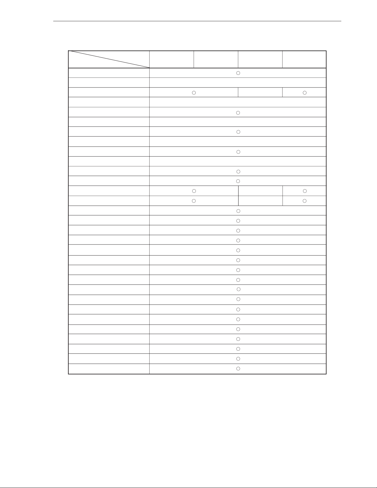
CHAPTER 6 PERIPHERAL HARDWARE FUNCTION
Table 6-2. I/O Pin Manipulation Instructions
PORT PORT3 PORT6 PORT7 PORT8
Instruction
Note 1
Note 1
Note 1
Note 1
Note 1
Note 1
Note 1
Note 1
Note 1
Note 1
Note 1
Note 2
Note 2
Note 2
Note 2
Note 2
–
–
–
–
–
Note 2
Note 2
Note 2
Note 2
Note 2
IN A, PORTn
IN XA, PORTn
OUT PORTn, A
OUT PORTn, XA
MOV A, PORTn
MOV XA, PORTn
MOV PORTn, A
MOV PORTn, XA
XCH A, PORTn
XCH XA, PORTn
MOV1 CY, PORTn. bit
MOV1 CY, PORTn. @L
MOV1 PORTn. bit, CY –
MOV1 PORTn. @L, CY
INCS PORTn
SET1 PORTn. bit
SET1 PORTn. @L
CLR1 PORTn. bit
CLR1 PORTn. @L
SKT PORTn. bit
SKT PORTn. @L
SKF PORTn. bit
SKTCLR PORTn. bit
SKTCLR PORTn. @L
SKF PORTn. @L
AND1 CY, PORTn. bit
AND1 CY, PORTn. @L
OR1 CY, PORTn. bit
OR1 CY, PORTn. @L
XOR1 CY, PORTn. bit
XOR1 CY, PORTn. @L
–
–
Notes 1. Must be MBE = 0 or (MBE = 1, MBS = 15) before execution.
2. The lower 2 bits and the bit addresses of the address must be indirectly specified by the L register.
User’s Manual U10676EJ3V0UM
97
Page 98

CHAPTER 6 PERIPHERAL HARDWARE FUNCTION
6.1.4 Operation of digital I/O port
The operations of each port and port pin when a data memory manipulation instruction is executed to manipulate
a digital I/O port differ depending on whether the port is set to the input or output mode (refer to Table 6-3). This
is because, as can be seen from the configuration of the I/O port, the data of each pin is loaded to the internal bus
in the input mode, and the data of the output latch is loaded to the internal bus in the output mode.
(1) Operation in input mode
When a test instruction such as SKT, a bit input instruction such as MOV1, or an instruction that loads port
data to the internal bus in 4-bit units such as IN, MOV, operation, or comparison instructions, is executed,
the data of each pin is manipulated.
When an instruction that transfers the contents of the accumulator in 4-bit units, such as OUT or MOV, is
executed, the data of the accumulator is latched to the output latch. The output buffer remains off.
When the XCH instruction is executed, the data of each pin is input to the accumulator, and the data of the
accumulator is latched to the output latch. The output buffer remains off.
When the INCS instruction is executed, the data (4 bits) of each pin incremented by one (+1) is latched to
the output latch. The output buffer remains off.
When an instruction that rewrites the data memory contents in 1-bit units, such as SET1, CLR1, MOV1, or
SKTCLR, is executed, the contents of the output latch of the specified bit can be rewritten as specified by the
instruction, but the contents of the output latches of the other bits are undefined.
(2) Operation in output mode
When a test instruction, bit input instruction, or an instruction in 4-bit units that loads port data to the internal
bus is executed, the contents of the output latch are manipulated.
When an instruction that transfers the contents of the accumulator in 4-bit units is executed, the data of the
output latch is rewritten and at the same time output from the port pins.
When the XCH instruction is executed, the contents of the output latch are transferred to the accumulator.
The contents of the accumulator are latched to the output latches of the specified port and output from the
port pins.
When the INCS instruction is executed, the contents of the output latches of the specified port are incremented
by 1 and output from the port pins.
When a bit output instruction is executed, the specified bit of the output latch is rewritten and output from the
pin.
98 User’s Manual U10676EJ3V0UM
Page 99
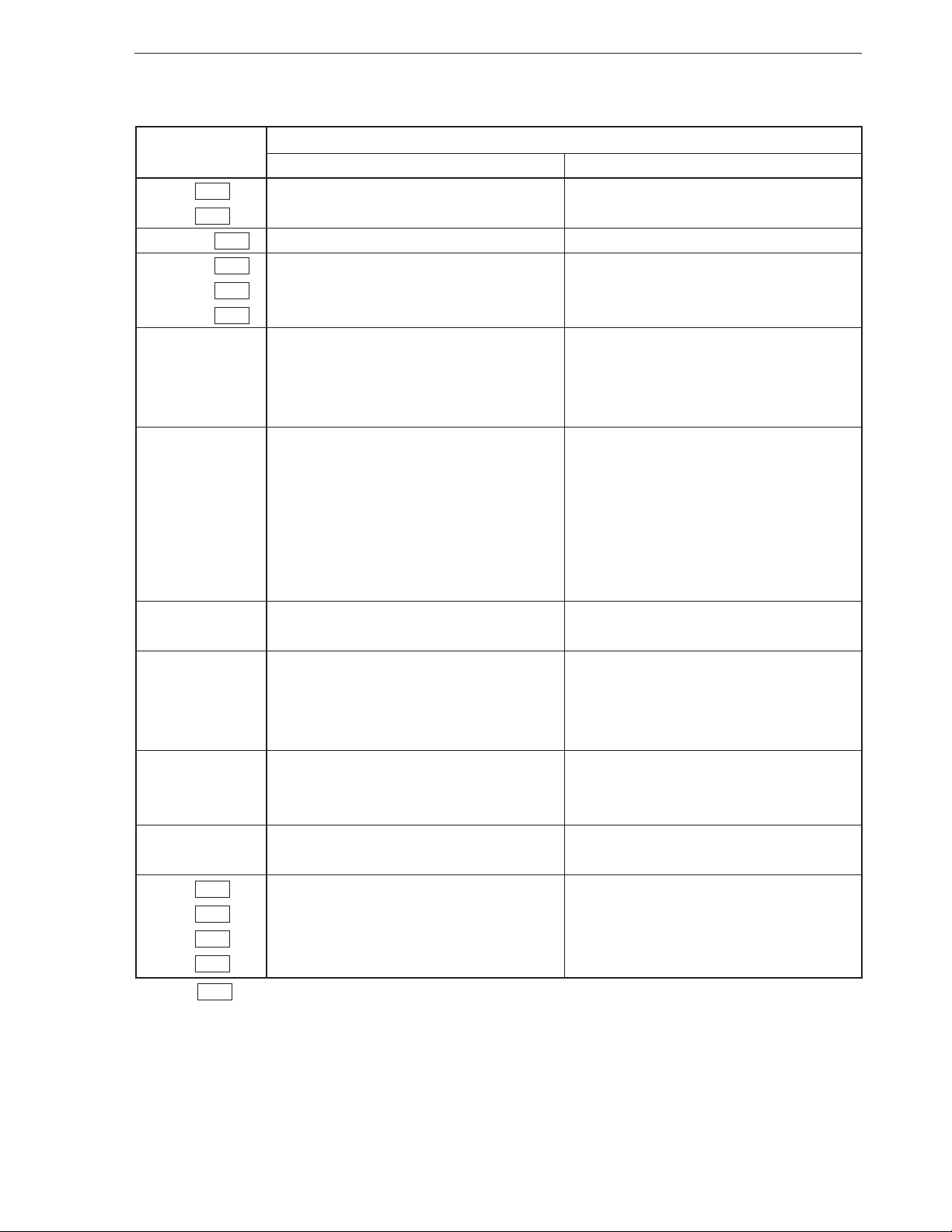
CHAPTER 6 PERIPHERAL HARDWARE FUNCTION
Table 6-3. Operation When I/O Port Is Manipulated
Instruction Executed
SKT <1> Tests pin data Tests output latch data
SKF <1>
MOV1 CY, <1> Transfers pin data to CY Transfers output latch data to CY
AND1 CY, <1> Performs operation between pin data and CY Performs operation between output latch data
OR1 CY, <1> and CY
XOR1 CY, <1>
IN A, PORTn Transfers pin data to accumulator Transfers output latch data to accumulator
MOV A, PORTn
MOV A, @HL
MOV XA, @HL
ADDS A, @HL Performs operation between pin data and Performs operation between output latch data
ADDC A, @HL accumulator and accumulator
SUBS A, @HL
SUBC A, @HL
AND A, @HL
OR A, @HL
XOR A, @HL
SKE A, @HL Compares pin data with accumulator Compares output latch data with accumulator
SKE XA, @HL
OUT PORTn, A Transfers accumulator data to output latch Transfers accumulator data to output latch and
MOV PORTn, A (output buffer remains off) outputs data from pins
MOV @HL, A
MOV @HL, XA
XCH A, PORTn
XCH A, @HL data to output latch (output buffer remains off) accumulator
XCH XA, @HL
INCS PORT Increments pin data by 1 and latches it to output Increments output latch contents by 1
INCS @HL latch
SET1 <1> Rewrites output latch contents of specified bit as Changes status of output pin as specified by
CLR1 <1> specified by instruction. However, output latch instruction
MOV1 <1> , CY contents of other bits are undefined
SKTCLR <1>
Transfers pin data to accumulator and accumulator
Input mode Output mode
Operation of Port and Pin
Exchanges data between output latch and
Remark <1> : Indicates two addressing modes: PORTn, bit and PORTn.@L.
User’s Manual U10676EJ3V0UM
99
Page 100

CHAPTER 6 PERIPHERAL HARDWARE FUNCTION
(
)
6.1.5 Connecting pull-up resistor
Each port pin of the µPD754244 can be connected to a pull-up resistor. Some pins can be connected to a pull-
up resistor via software and others can be connected by a mask option.
Table 6-4 shows how to specify the connection of the pull-up resistor to each port pin. The pull-up resistor is
connected via software in the format shown in Figure 6-11.
The pull-up resistor can be connected only to the pins of ports 3, 6, and 8 in the input mode. When the pins are
set to the output mode, the pull-up resistor cannot be connected regardless of the setting of POGA and POGB.
Table 6-4. Specifying Connection of Pull-up Resistor
Port (Pin Name) Specifying Connection of Pull-up Resistor Specified Bit
Port 3 (P30-P33) Connection of pull-up resistor specified in 4-bit POGA.3
Port 6 (P60-P63)
units via software
POGA.6
Port 7 (P70-P73) Connection of pull-up resistor specified in 1-bit —
units by mask option
Port 8 (P80-P83) Connection of pull-up resistor specified in 1-bit POGB.0
units via software
Figure 6-11. Format of Pull-up Resistor Specification Register
0 Pull-up resistor not connected
1 Pull-up resistor connected
Pull-up resistor specification register group A
Address
FDCH
765432
Pull-up resistor specification register group B
Address
FDEH
765432
Specification
10
––PO3 –––PO6–
10
PO8–––––––
Symbol
POGA
Port 3 (P30 to P33)
Port 6 (P60 to P63)
Symbol
POGB
Port 8
P80
100 User’s Manual U10676EJ3V0UM
 Loading...