

Page 1
µ
PD17134A SUBSERIES
4-BIT SINGLE-CHIP MICROCONTROLLER
µ
PD17134A
µ
PD17135A
µ
PD17136A
µ
PD17137A
µ
PD17P136A
µ
PD17P137A
Document No. U11607EJ3V0UM00 (3rd edition)
Date Published December 1996 N
©
1993
Printed in Japan
Page 2

NOTES FOR CMOS DEVICES
1 PRECAUTION AGAINST ESD FOR SEMICONDUCTORS
Note:
Strong electric field, when exposed to a MOS device, can cause destruction of the gate oxide and
ultimately degrade the device operation. Steps must be taken to stop generation of static electricity
as much as possible, and quickly dissipate it once, when it has occurred. Environmental control
must be adequate. When it is dry, humidifier should be used. It is recommended to avoid using
insulators that easily build static electricity. Semiconductor devices must be stored and transported
in an anti-static container, static shielding bag or conductive material. All test and measurement
tools including work bench and floor should be grounded. The operator should be grounded using
wrist strap. Semiconductor devices must not be touched with bare hands. Similar precautions
need to be taken for PW boards with semiconductor devices on it.
2 HANDLING OF UNUSED INPUT PINS FOR CMOS
Note:
No connection for CMOS device inputs can be cause of malfunction. If no connection is provided
to the input pins, it is possible that an internal input level may be generated due to noise, etc., hence
causing malfunction. CMOS devices behave differently than Bipolar or NMOS devices. Input
levels of CMOS devices must be fixed high or low by using a pull-up or pull-down circuitry. Each
unused pin should be connected to V
possibility of being an output pin. All handling related to the unused pins must be judged device
by device and related specifications governing the devices.
DD or GND with a resistor, if it is considered to have a
3 STATUS BEFORE INITIALIZATION OF MOS DEVICES
Note:
Power-on does not necessarily define initial status of MOS device. Production process of MOS
does not define the initial operation status of the device. Immediately after the power source is
turned ON, the devices with reset function have not yet been initialized. Hence, power-on does
not guarantee out-pin levels, I/O settings or contents of registers. Device is not initialized until
the reset signal is received. Reset operation must be executed immediately after power-on for
devices having reset function.
Page 3

Regional Information
Some information contained in this document may vary from country to country. Before using any NEC
product in your application, please contact the NEC office in your country to obtain a list of authorized
representatives and distributors. They will verify:
• Device availability
• Ordering information
• Product release schedule
• Availability of related technical literature
• Development environment specifications (for example, specifications for third-party tools and
components, host computers, power plugs, AC supply voltages, and so forth)
• Network requirements
In addition, trademarks, registered trademarks, export restrictions, and other legal issues may also vary
from country to country.
NEC Electronics Inc. (U.S.)
Santa Clara, California
Tel: 800-366-9782
Fax: 800-729-9288
NEC Electronics (Germany) GmbH
Duesseldorf, Germany
Tel: 0211-65 03 02
Fax: 0211-65 03 490
NEC Electronics (UK) Ltd.
Milton Keynes, UK
Tel: 01908-691-133
Fax: 01908-670-290
NEC Electronics Italiana s.r.1.
Milano, Italy
Tel: 02-66 75 41
Fax: 02-66 75 42 99
NEC Electronics (Germany) GmbH
Benelux Office
Eindhoven, The Netherlands
Tel:040-2445845
Fax: 040-2444580
NEC Electronics (France) S.A.
Velizy-Villacoublay, France
Tel:01-30-67 58 00
Fax: 01-30-67 58 99
NEC Electronics (France) S.A.
Spain Office
Madrid, Spain
Tel: 01-504-2787
Fax: 01-504-2860
NEC Electronics (Germany) GmbH
Scandinavia Office
Taeby, Sweden
Tel: 08-63 80 820
Fax: 08-63 80 388
NEC Electronics Hong Kong Ltd.
Hong Kong
Tel:2886-9318
Fax: 2886-9022/9044
NEC Electronics Hong Kong Ltd.
Seoul Branch
Seoul, Korea
Tel: 02-528-0303
Fax: 02-528-4411
NEC Electronics Singapore Pte. Ltd.
United Square, Singapore 1130
Tel:253-8311
Fax: 250-3583
NEC Electronics Taiwan Ltd.
Taipei, Taiwan
Tel: 02-719-2377
Fax: 02-719-5951
NEC do Brasil S.A.
Sao Paulo-SP, Brasil
Tel: 011-889-1680
Fax: 011-889-1689
J96. 8
Page 4

SIMPLEHOST
is a trademark of NEC Corp.
MS-DOS and Windows are trademarks of Microsoft Corp.
PC/AT and PC DOS are trademarks of IBM Corp.
The export of this product from Japan is prohibited without governmental license. To export or re-export this product from
a country other than Japan may also be prohibited without a license from that country. Please call an NEC sales
representative.
The information in this document is subject to change without notice.
No part of this document may be copied or reproduced in any form or by any means without the prior written
consent of NEC Corporation. NEC Corporation assumes no responsibility for any errors which may appear in
this document.
NEC Corporation does not assume any liability for infringement of patents, copyrights or other intellectual property
rights of third parties by or arising from use of a device described herein or any other liability arising from use
of such device. No license, either express, implied or otherwise, is granted under any patents, copyrights or other
intellectual property rights of NEC Corporation or others.
While NEC Corporation has been making continuous effort to enhance the reliability of its semiconductor devices,
the possibility of defects cannot be eliminated entirely. To minimize risks of damage or injury to persons or
property arising from a defect in an NEC semiconductor device, customers must incorporate sufficient safety
measures in its design, such as redundancy, fire-containment, and anti-failure features.
NEC devices are classified into the following three quality grades:
"Standard", "Special", and "Specific". The Specific quality grade applies only to devices developed based on a
customer designated “quality assurance program“ for a specific application. The recommended applications of
a device depend on its quality grade, as indicated below. Customers must check the quality grade of each device
before using it in a particular application.
Standard: Computers, office equipment, communications equipment, test and measurement equipment,
audio and visual equipment, home electronic appliances, machine tools, personal electronic
equipment and industrial robots
Special: Transportation equipment (automobiles, trains, ships, etc.), traffic control systems, anti-disaster
systems, anti-crime systems, safety equipment and medical equipment (not specifically designed
for life support)
Specific: Aircrafts, aerospace equipment, submersible repeaters, nuclear reactor control systems, life
support systems or medical equipment for life support, etc.
The quality grade of NEC devices is "Standard" unless otherwise specified in NEC's Data Sheets or Data Books.
If customers intend to use NEC devices for applications other than those specified for Standard quality grade,
they should contact an NEC sales representative in advance.
Anti-radioactive design is not implemented in this product.
M7 96.5
Page 5

Major Revisions in This Edition
Page Description
Throughout Change of name µPD1713XA to µPD17134A subseries
p. 5 Correction of (2) Program memory write/verify mode in 1.4 PIN CONFIGURATION
p. 18 Change of Figure 3-2 Value of Program Counter after Instruction
Partial correction of 3.2.2 On Execution of Branch Instruction (BR)
p. 19 Partial correction of 3.2.3 On During Execution of Subroutine Call
p. 23 Change of CHAPTER 4 PROGRAM MEMORY (ROM)
p. 31 Partial correction of Figure 5-1 Data Memory Configuration
p. 35 Change of CHAPTER 6 STACK
p. 43 Partial correction of 7.2.2 Address Register Functions
p. 47 Change of 7.5 INDEX REGISTER (IX) AND DATA MEMORY ROW ADDRESS
POINTER (MEMORY POINTER: MP)
p. 58 Partial change of 7.6.2 Functions of General Register Pointer
p. 59 Partial change of 7.7.1 Program Status Word Configuration
p. 61 Change of 7.7.4 Zero Flag (Z) and Compare Flag (CMP)
p. 61 Partial correction of 7.7.5 Carry Flag (CY)
p. 71 Partial correction of 9.2.3 Register File Manipulation Instructions
p. 111 Change of CHAPTER 13 PERIPHERAL HARDWARE
p. 149 Change of CHAPTER 14 INTERRUPT FUNCTIONS
p. 169 Change of CHAPTER 16 STANDBY FUNCTION
p. 179 Change of CHAPTER 17 RESET
p. 190 Partial change of Table 18-2 Differences between Mask ROM Version and One-
Time PROM Version
p. 194 Partial change of 19.3 LIST OF THE INSTRUCTION SET
p. 198 Partial change of 19.5 INSTRUCTIONS
p. 255 Change of CHAPTER 20 ASSEMBLER RESERVED WORDS
p. 257 Partial change of 20.2 RESERVED SYMBOLS
p. 261 Addition of APPENDIX A DEVELOPMENT OF µPD171×× SUBSERIES
p. 263 Addition of APPENDIX B COMPARISON OF FUNCTIONS BETWEEN µPD17135A,
17137A, AND µPD17145 SUBSERIES
p. 267 Addition of APPENDIX D NOTES ON CONFIGURATION OF SYSTEM CLOCK
OSCILLATION CIRCUIT
The mark shows major revisions made in this edition.
Page 6

PREFACE
Target : This manual is intended for user engineers who understand the functions of each product in
the µPD17134A subseries and try to design application systems using the µPD17134A
subseries.
Purpose : The purpose of this manual is for the user to understand the hardware functions of the
µ
PD17134A subseries.
Use : The manual assumes that the reader has a general knowledge of electricity, logic circuits,
microcomputers.
µ
• To understand the functions of the
→ Read the manual from CONTENTS.
• To look up instruction functions in detail when you know the mnemonic of an
instruction;
→ Use APPENDIX E INSTRUCTION LIST.
• To look up an instruction when you do not know its mnemonic but know outlines of
the function;
→ Refer to 19.3 LIST OF THE INSTRUCTION SET for search for the mnemonic of the
instruction, then see 19.5 INSTRUCTIONS for the functions.
PD17134A subseries in a general way;
µ
• To learn the electrical specifications of the
PD17134A subseries
→ Refer to the Data Sheet available separately.
µ
• To learn the application examples of the functions of the
PD17134A subseries
→ Refer to the Application Note available separately.
Legend : Data representation weight : High-order and low-order digits are indicated from left to right.
Active low representation : ××× (pin or signal name is overlined)
Memory map address : Top: low-order, bottom: high-order
Note
Note : Explanation of
in the text
Caution : Caution to which you should pay attention
Remark : Supplementary explanation to the text
Number representation : Binary number ...×××× or ××××B
Decimal number ...××××
Hexadecimal number ...××××H
Page 7
Related Documents : The following documents are provided for the µPD17134A subseries.
The numbers listed in the table are the document numbers.
Product name
µ
PD17134AµPD17135AµPD17136AµPD17137AµPD17P136AµPD17P137A
Document name
Brochure IF-1166 IF-1169 IF-1166 IF-1169 IF-1168 IF-1165
Data sheet U10591E U10592E U10591E U10592E IC-2871 IC-2872
User’s manual IEU-1369
Application note IEA-1297 (Introduction), IEA-1293 (Rice cooker, thermos bottle)
IE-17K (Ver. 1.6) EEU-1467
user’s manual
IE-17K-ET (Ver. 1.6) EEU-1466
user’s manual
SE board EEU-1379
user’s manual
SIMPLEHOST
user’s manual
AS17K assembler EEU-1287
user’s manual
Device file U10777E
user’s manual
TM
EEU-1336 (Introduction), EEU-1337 (Reference)
Pin name and symbol name should be read according to the system clock type.
System clock RC oscillation Ceramic oscillation
µ
PD17134A
µ
PD17136A
Pin name, symbol name
Pin for system clock oscillation OSC1 XIN
System clock fCC fX
µ
PD17P136A
OSC0 XOUT
µ
PD17135A
µ
PD17137A
µ
PD17P137A
Page 8

TABLE OF CONTENTS
CHAPTER 1 GENERAL DESCRIPTION ................................................................................................. 1
1.1 FUNCTION LIST ........................................................................................................................................ 2
1.2 ORDERING INFORMATION ..................................................................................................................... 3
1.3 BLOCK DIAGRAM .................................................................................................................................... 4
1.4 PIN CONFIGURATION (TOP VIEW) ........................................................................................................ 5
CHAPTER 2 PIN FUNCTIONS ............................................................................................................... 9
2.1 PIN FUNCTIONS ....................................................................................................................................... 9
2.2 PIN INPUT/OUTPUT CIRCUIT ............................................................................................................... 11
2.3 PROCESSING OF UNUSED PINS ......................................................................................................... 14
2.4 NOTES ON USING RESET PIN AND P1B
0 PIN ................................................................................... 15
CHAPTER 3 PROGRAM COUNTER (PC) ........................................................................................... 17
3.1 PROGRAM COUNTER CONFIGURATION............................................................................................ 17
3.2 PROGRAM COUNTER OPERATION ..................................................................................................... 17
3.2.1 At Reset ..................................................................................................................................... 18
3.2.2 During Execution of the Branch Instruction (BR)..................................................................... 18
3.2.3 During Execution of Subroutine Calls (CALL).......................................................................... 1 9
3.2.4 During Execution of Return Instructions (RET, RETSK, RETI)............................................... 20
3.2.5 During Table Reference (MOVT) .............................................................................................. 20
3.2.6 During Execution of Skip Instructions (SKE, SKGE, SKLT, SKNE, SKT, SKF)...................... 21
3.2.7 When an Interrupt Is Received ................................................................................................. 2 1
CHAPTER 4 PROGRAM MEMORY (ROM) .......................................................................................... 23
4.1 PROGRAM MEMORY CONFIGURATION ............................................................................................. 23
4.2 PROGRAM MEMORY USAGE ............................................................................................................... 24
4.2.1 Flow of the Program.................................................................................................................. 24
4.2.2 Table Reference......................................................................................................................... 27
CHAPTER 5 DATA MEMORY (RAM) .................................................................................................... 31
5.1 DATA MEMORY CONFIGURATION....................................................................................................... 31
5.1.1 System Register (SYSREG) ..................................................................................................... 32
5.1.2 Data Buffer (DBF)...................................................................................................................... 32
5.1.3 General Register (GR) .............................................................................................................. 33
5.1.4 Port Registers............................................................................................................................ 33
5.1.5 General Data Memory ............................................................................................................... 34
5.1.6 Unmounted Data Memory ......................................................................................................... 3 4
- i -
Page 9

CHAPTER 6 STACK .............................................................................................................................. 3 5
6.1 STACK CONFIGURATION ...................................................................................................................... 35
6.2 FUNCTIONS OF THE STACK ................................................................................................................ 35
6.3 ADDRESS STACK REGISTERS (ASRs)............................................................................................... 3 6
6.4 INTERRUPT STACK REGISTERS (INTSKs) ........................................................................................ 36
6.5 STACK POINTER (SP) AND INTERRUPT STACK REGISTERS ........................................................ 37
6.6 STACK OPERATION ............................................................................................................................... 38
6.6.1 On Execution of Instructions CALL, RET, RETSK................................................................... 38
6.6.2 Table Reference (MOVT DBF, @AR Instruction) ..................................................................... 3 8
6.6.3 Operation on Execution of Interrupt Receipt and RETI Instruction ......................................... 39
6.7 STACK NESTING LEVELS AND THE PUSH AND POP INSTRUCTIONS ......................................... 39
CHAPTER 7 SYSTEM REGISTER (SYSREG) .................................................................................... 41
7.1 SYSTEM REGISTER CONFIGURATION............................................................................................... 41
7.2 ADDRESS REGISTER (AR) ................................................................................................................... 43
7.2.1 Address Register Configuration................................................................................................ 43
7.2.2 Address Register Functions...................................................................................................... 43
7.3 WINDOW REGISTER (WR) .................................................................................................................... 45
7.3.1 Window Register Configuration ................................................................................................ 45
7.3.2 Window Register Functions ...................................................................................................... 45
7.4 BANK REGISTER (BANK) ..................................................................................................................... 46
7.4.1 Bank Register Configuration ..................................................................................................... 46
7.4.2 Functions of Bank Register....................................................................................................... 46
7.5 INDEX REGISTER (IX) AND DATA MEMORY ROW ADDRESS POINTER
(MEMORY POINTER: MP)...................................................................................................................... 47
7.5.1 Index Register (IX) .................................................................................................................... 47
7.5.2 Data Memory Row Address Pointer (Memory Pointer: MP).................................................... 47
7.5.3 IXE = 0 and MPE = 0 (No Data Memory Modification) ........................................................... 49
7.5.4 IXE = 0 and MPE = 1 (Diagonal Indirect Data Transfer)......................................................... 51
7.5.5 IXE = 1 and MPE = 0 (Index Modification) ............................................................................... 53
7.6 GENERAL REGISTER POINTER (RP) .................................................................................................. 57
7.6.1 General Register Pointer Configuration ................................................................................... 57
7.6.2 Functions of the General Register Pointer............................................................................... 58
7.7 PROGRAM STATUS WORD (PSWORD) ............................................................................................... 59
7.7.1 Program Status Word Configuration......................................................................................... 5 9
7.7.2 Functions of the Program Status Word .................................................................................... 60
7.7.3 Index Enable Flag (IXE)............................................................................................................ 61
7.7.4 Zero Flag (Z) and Compare Flag (CMP) .................................................................................. 61
7.7.5 Carry Flag (CY) ......................................................................................................................... 61
7.7.6 Binary-Coded Decimal Flag (BCD)........................................................................................... 6 2
7.7.7 Notes Concerning Use of Arithmetic Operations ..................................................................... 62
7.8 NOTES CONCERNING USE OF THE SYSTEM REGISTER ............................................................... 6 3
7.8.1 Reserved Words for the System Register................................................................................ 63
7.8.2 Handling of System Register Addresses Fixed at 0 ................................................................ 6 5
- ii -
Page 10

CHAPTER 8 GENERAL REGISTER (GR) ........................................................................................... 67
8.1 GENERAL REGISTER CONFIGURATION ............................................................................................ 67
8.2 FUNCTIONS OF THE GENERAL REGISTER....................................................................................... 67
CHAPTER 9 REGISTER FILE (RF)...................................................................................................... 69
9.1 REGISTER FILE CONFIGURATION ...................................................................................................... 69
9.1.1 Configuration of the Register File............................................................................................. 69
9.1.2 Relationship between the Register File and Data Memory..................................................... 69
9.2 FUNCTIONS OF THE REGISTER FILE................................................................................................. 70
9.2.1 Functions of the Register File................................................................................................... 70
9.2.2 Functions of Control Register ................................................................................................... 70
9.2.3 Register File Manipulation Instructions .................................................................................... 71
9.3 CONTROL REGISTER ............................................................................................................................ 72
9.4 NOTES CONCERNING USE OF THE REGISTER FILE....................................................................... 73
9.4.1 Notes Concerning Operation of the Control Register (Read-Only and Unused Registers) ... 73
9.4.2 Register File Symbol Definitions and Reserved Words........................................................... 7 3
CHAPTER 10 DATA BUFFER (DBF) ................................................................................................... 77
10.1 DATA BUFFER CONFIGURATION ........................................................................................................ 7 7
10.2 FUNCTIONS OF THE DATA BUFFER ................................................................................................... 78
10.2.1 Data Buffer and Peripheral Hardware ...................................................................................... 7 9
10.2.2 Data Transfer with Peripheral Hardware.................................................................................. 80
10.2.3 Table Reference......................................................................................................................... 81
CHAPTER 11 ARITHMETIC AND LOGIC UNIT (ALU) ....................................................................... 83
11.1 ALU BLOCK CONFIGURATION ............................................................................................................ 83
11.2 FUNCTIONS OF THE ALU BLOCK ....................................................................................................... 83
11.2.1 Functions of the ALU................................................................................................................. 83
11.2.2 Functions of Temporary Registers A and B.............................................................................. 88
11.2.3 Functions of the Status Flip-flop............................................................................................... 88
11.2.4 Operations in 4-Bit Binary ......................................................................................................... 89
11.2.5 Operations in BCD ..................................................................................................................... 89
11.2.6 Operations in the ALU Block..................................................................................................... 9 0
11.3 ARITHMETIC OPERATIONS (ADDITION AND SUBTRACTION IN 4-BIT BINARY AND BCD) ....... 91
11.3.1 Addition and Subtraction When CMP = 0 and BCD = 0.......................................................... 9 1
11.3.2 Addition and Subtraction When CMP = 1 and BCD = 0.......................................................... 9 1
11.3.3 Addition and Subtraction When CMP = 0 and BCD = 1.......................................................... 9 2
11.3.4 Addition and Subtraction When CMP = 1 and BCD = 1.......................................................... 9 2
11.3.5 Notes Concerning Use of Arithmetic Operations ..................................................................... 92
11.4 LOGICAL OPERATIONS ........................................................................................................................ 93
11.5 BIT JUDGEMENTS ................................................................................................................................. 94
11.5.1 TRUE (1) Bit Judgement ........................................................................................................... 94
11.5.2 FALSE (0) Bit Judgement ......................................................................................................... 95
- iii -
Page 11

11.6 COMPARISON JUDGEMENTS .............................................................................................................. 96
11.6.1 “Equal to” Judgement ................................................................................................................ 96
11.6.2 “Not Equal to” Judgement ......................................................................................................... 97
11.6.3 “Greater Than or Equal to” Judgement .................................................................................... 97
11.6.4 “Less Than” Judgement ............................................................................................................ 98
11.7 R OTATIONS ............................................................................................................................................. 99
11.7.1 Rotation to the Right ................................................................................................................. 99
11.7.2 Rotation to the Left.................................................................................................................. 100
CHAPTER 12 PORTS ......................................................................................................................... 1 01
12.1 PORT 0A (P0A0, P0A1, P0A2, P0A3).................................................................................................... 10 1
12.2 PORT 0B (P0B0, P0B1, P0B2, P0B3).................................................................................................... 10 2
12.3 PORT 0C (P0C0/ADC0, P0C1/ADC1, P0C2/ADC2, P0C3/ADC3) .......................................................... 103
12.4 PORT 0D (P0D
12.5 PORT 1A (P1A0, P1A1, P1A2, P1A3).................................................................................................... 10 5
12.6 PORT 1B (P1B0).................................................................................................................................... 105
12.7 PORT CONTROL REGISTER ............................................................................................................... 106
12.7.1 Input/Output Switching by Group I/O...................................................................................... 106
12.7.2 Input/Output Switching by Bit I/O ........................................................................................... 107
12.7.3 Specifying Pull-Up Resistor Incorporation Using Software ................................................... 109
0/SCK, P0D1/SO, P0D2/SI, P0D3/TM0OUT)................................................................ 104
CHAPTER 13 PERIPHERAL HARDWARE ......................................................................................... 111
13.1 8-BIT TIMERS/COUNTERS (TM0 and TM1)........................................................................................111
13.1.1 8-Bit Timers/Counters Configuration .......................................................................................111
13.1.2 Operation of 8-Bit Timers/Counters........................................................................................ 115
13.1.3 Selecting Count Pulse ............................................................................................................. 115
13.1.4 Setting Count Value to Modulo Register................................................................................ 116
13.1.5 Reading Value of Count Register ........................................................................................... 117
13.1.6 Setting of Interval Time ........................................................................................................... 118
13.1.7 Error of Interval Time............................................................................................................... 119
13.1.8 Timer 0 Output......................................................................................................................... 121
13.2 BASIC INTERVAL TIMER (BTM) ......................................................................................................... 122
13.2.1 Basic Interval Timer Configuration .......................................................................................... 122
13.2.2 Registers Controlling Basic Interval Timer ............................................................................. 123
13.2.3 Operation of Basic Interval Timer ........................................................................................... 124
13.2.4 Watchdog Timer Function ....................................................................................................... 125
13.3 A/D CONVERTER ................................................................................................................................. 128
13.3.1 A/D Converter Configuration ................................................................................................... 128
13.3.2 Functions of A/D Converter..................................................................................................... 129
13.3.3 Setting Values in the 8-bit Data Register (ADCR) ................................................................. 132
13.3.4 Reading Values from the 8-bit Data Register (ADCR) .......................................................... 133
13.3.5 A/D Converter Operation......................................................................................................... 134
13.4 SERIAL INTERFACE (SIO) .................................................................................................................. 141
13.4.1 Functions of the Serial Interface............................................................................................. 141
13.4.2 3-wire Serial Interface Operation Modes................................................................................ 14 3
13.4.3 Setting Values in the Shift Register........................................................................................ 147
13.4.4 Reading Values from the Shift Register ................................................................................. 148
- iv -
Page 12

CHAPTER 14 INTERRUPT FUNCTIONS............................................................................................ 14 9
14.1 INTERRUPT SOURCE TYPES AND VECTOR ADDRESSES............................................................ 15 0
14.2 HARDWARE COMPONENTS OF THE INTERRUPT CONTROL CIRCUIT ....................................... 151
14.3 INTERRUPT SEQUENCE ..................................................................................................................... 158
14.3.1 Receiving an Interrupt ............................................................................................................. 158
14.3.2 Return from the Interrupt Routine........................................................................................... 159
14.3.3 Interrupt Accepting Timing ...................................................................................................... 160
14.4 MULTI-INTERRUPT............................................................................................................................... 163
14.5 PROGRAM EXAMPLE OF INTERRUPT ............................................................................................. 164
CHAPTER 15 AC ZERO CROSS DETECTION .................................................................................. 167
CHAPTER 16 STANDBY FUNCTION.................................................................................................. 16 9
16.1 OVERVIEW OF THE STANDBY FUNCTION ....................................................................................... 16 9
16.2 HALT MODE .......................................................................................................................................... 170
16.2.1 Setting HALT Mode ................................................................................................................. 1 70
16.2.2 Star t Address after HALT Mode Is Released ......................................................................... 170
16.2.3 HALT Mode Setting Conditions ............................................................................................... 172
16.3 STOP MODE.......................................................................................................................................... 174
16.3.1 Setting of STOP Mode ............................................................................................................ 174
16.3.2 Star t Address after STOP Mode Is Released ........................................................................ 174
16.3.3 STOP Mode Setting Conditions.............................................................................................. 176
CHAPTER 17 RESET ........................................................................................................................... 17 9
17.1 RESET FUNCTION ................................................................................................................................ 180
17.2 RESETTING ........................................................................................................................................... 181
17.3 POWER-ON/POWER-DOWN RESET FUNCTION .............................................................................. 18 2
17.3.1 Conditions Required to Enable the Power-On Reset Function............................................. 182
17.3.2 Power-On Reset Function and Operation .............................................................................. 183
17.3.3 Condition Required for Use of the Power-Down Reset Function.......................................... 18 5
17.3.4 Power-Down Reset Function and Operation.......................................................................... 18 5
CHAPTER 18 ONE-TIME PROM WRITING/VERIFYING .................................................................... 189
18.1 DIFFERENCES BETWEEN MASK ROM VERSION AND ONE-TIME PROM MODEL..................... 1 89
18.2 OPERATION MODE WHEN PROGRAM MEMORY IS WRITTEN/VERIFIED ................................... 190
18.3 WRITING PROCEDURE OF PROGRAM MEMORY ........................................................................... 191
18.4 READING PROCEDURE OF PROGRAM MEMORY .......................................................................... 192
CHAPTER 19 INSTRUCTION SET ...................................................................................................... 193
19.1 OVERVIEW OF THE INSTRUCTION SET........................................................................................... 193
19.2 LEGEND ................................................................................................................................................. 194
19.3 LIST OF THE INSTRUCTION SET....................................................................................................... 195
19.4 ASSEMBLER (AS17K) EMBEDDED MACRO INSTRUCTIONS ........................................................ 197
- v -
Page 13

19.5 INSTRUCTIONS .................................................................................................................................... 198
19.5.1 Addition Instructions ................................................................................................................ 1 98
19.5.2 Subtraction Instructions........................................................................................................... 209
19.5.3 Logical Operation Instructions ................................................................................................ 216
19.5.4 Judgment Instructions ............................................................................................................. 221
19.5.5 Comparison Instructions.......................................................................................................... 223
19.5.6 Rotation Instructions................................................................................................................ 226
19.5.7 Transfer Instructions ................................................................................................................ 227
19.5.8 Branch Instructions.................................................................................................................. 243
19.5.9 Subroutine Instructions............................................................................................................ 246
19.5.10 Interrupt Instructions................................................................................................................ 251
19.5.11 Other Instructions .................................................................................................................... 253
CHAPTER 20 ASSEMBLER RESERVED WORDS ............................................................................255
20.1 MASK OPTION DIRECTIVE ................................................................................................................. 25 5
20.1.1 Specifying Mask Option .......................................................................................................... 255
20.2 RESERVED SYMBOLS......................................................................................................................... 257
APPENDIX A DEVELOPMENT OF µPD171×× SUBSERIES .............................................................26 1
APPENDIX B COMPARISON OF FUNCTIONS BETWEEN µPD17135A, 17137A, AND
µPD17145 SUBSERIES................................................................................................ 263
APPENDIX C DEVELOPMENT TOOLS .............................................................................................. 2 65
APPENDIX D NOTES ON CONFIGURATION OF SYSTEM CLOCK OSCILLATION CIRCUIT...... 267
APPENDIX E INSTRUCTION LIST...................................................................................................... 269
E.1 INSTRUCTION LIST (by function) ...................................................................................................... 2 69
E.2 IINSTRUCTION LIST (alphabetical order) ......................................................................................... 270
APPENDIX F ORDERING MASK ROM............................................................................................... 27 1
- vi -
Page 14

LIST OF FIGURES (1/3)
Figure No. Title Page
3-1 Program Counter...................................................................................................................................... 17
3-2 Value of the Program Counter after Instruction Execution .................................................................... 1 8
3-3 Value in the Program Counter after Reset ............................................................................................. 18
3-4 Value in the Program Counter during Execution of a BR addr Instruction ........................................... 18
3-5 Value in the Program Counter during Execution of an Indirect Branch Instruction.............................. 19
3-6 Value in the Program Counter during Execution of a CALL addr.......................................................... 1 9
3-7 Value in the Program Counter during Execution of an Indirect Subroutine Call .................................. 20
3-8 Value in the Program Counter during Execution of a Return Instruction.............................................. 20
µ
4-1 Program Memory Map for the
4-2 CALL addr Instruction .............................................................................................................................. 26
4-3 Table Reference (MOVT DBF, @AR)...................................................................................................... 27
5-1 Data Memory Configuration..................................................................................................................... 31
5-2 System Register Configuration................................................................................................................ 32
5-3 Data Buffer Configuration ........................................................................................................................ 32
5-4 General Register (GR) Configuration...................................................................................................... 33
5-5 Port Register Configuration ..................................................................................................................... 33
PD17134A Subseries ........................................................................... 2 3
6-1 Stack Configuration.................................................................................................................................. 35
7-1 Allocation of System Register in Data Memory...................................................................................... 41
7-2 System Register Configuration................................................................................................................ 42
7-3 Address Register Configuration .............................................................................................................. 43
7-4 Address Register Used as a Peripheral Circuit...................................................................................... 44
7-5 Window Register Configuration............................................................................................................... 45
7-6 Example of Window Register Operation ................................................................................................. 45
7-7 Bank Register Configuration ................................................................................................................... 46
7-8 Index Register Configuration ................................................................................................................... 47
7-9 Modification of Data Memor y Address by Index Register and Memory Pointer ................................... 48
7-10 Operation Example When IXE = 0 and MPE = 0................................................................................... 50
7-11 Operation Example When IXE = 0 and MPE = 1................................................................................... 52
7-12 Operation Example When IXE = 1 and MPE = 0................................................................................... 54
7-13 Operation Example When IXE = 1 and MPE = 0................................................................................... 55
7-14 Operation Example When IXE = 1 and MPE = 0 (Array Processing) ................................................... 56
7-15 General Register Pointer Configuration.................................................................................................. 57
7-16 General Register Configuration............................................................................................................... 58
7-17 Program Status Word Configuration ....................................................................................................... 59
7-18 Outline of Functions of the Program Status Word ................................................................................. 60
8-1 General Register Configuration............................................................................................................... 68
- vii -
Page 15

LIST OF FIGURES (2/3)
Figure No. Title Page
9-1 Register File Configuration ...................................................................................................................... 69
9-2 Relationship Between the Register File and Data Memory ................................................................... 7 0
9-3 Accessing the Register File Using the PEEK and POKE Instructions .................................................. 72
9-4 Control Register Configuration ................................................................................................................ 75
10-1 Allocation of the Data Buffer ................................................................................................................... 77
10-2 Data Buffer Configuration........................................................................................................................ 77
10-3 Relationship Between the Data Buffer and Peripheral Hardware ......................................................... 78
11-1 ALU Configuration.................................................................................................................................... 84
12-1 Input/Output Switching by Group I/O .................................................................................................... 106
12-2 Port Control Register of Bit I/O ............................................................................................................. 107
12-3 Specifying Pull-Up Resistor Incorporation Using Software.................................................................. 109
13-1 Configuration of the 8-Bit Timer Counters............................................................................................ 112
13-2 Timer 0 Mode Register .......................................................................................................................... 113
13-3 Timer 1 Mode Register .......................................................................................................................... 114
13-4 Setting Count Value to Modulo Register............................................................................................... 116
13-5 Reading Count Value of Count Register............................................................................................... 117
13-6 Error When Count Register Is Cleared to 0 During Counting ............................................................. 119
13-7 Error When Counting Is Started from Count Stop Status.................................................................... 120
13-8 Timer 0 Output Setting Register ............................................................................................................ 121
13-9 Basic Interval Timer Configuration........................................................................................................ 12 2
13-10 BTM Mode Register ............................................................................................................................... 123
13-11 Watchdog Timer Mode Register............................................................................................................ 124
13-12 Timing Char t of Watchdog Timer (with WDTRES Flag Used) ............................................................. 1 26
13-13 Block Diagram of the A/D Converter..................................................................................................... 128
13-14 A/D Converter Control Register ............................................................................................................ 130
13-15 Setting a Value in the 8-Bit Data Register (ADCR) .............................................................................. 13 2
13-16 Reading Values from the 8-bit Data Register (ADCR) ......................................................................... 1 33
13-17 Relationship between the Analog Input Voltage and Digital Conversion Result ................................ 134
13-18 Using the Successive Mode for the A/D Converter.............................................................................. 13 6
13-19 A/D Conversion Timing in the Continuous Mode ................................................................................. 137
13-20 Using the Single Mode for the A/D Converter ...................................................................................... 139
13-21 Single Mode Operation (Comparison) Timing ...................................................................................... 140
13-22 Block Diagram of the Serial Interface ................................................................................................... 142
13-23 Timing of 8-Bit Transmission and Reception Mode (Simultaneous Transmission and Reception) .. 143
13-24 Timing of the Clock Synchronization 8-Bit Reception Mode (SO Pin Output High Impedance)........ 144
13-25 Serial Interface Control Register ........................................................................................................... 145
13-26 Setting a Value in the Shift Register..................................................................................................... 147
13-27 Reading a Value from the Shift Register .............................................................................................. 14 8
- viii -
Page 16

LIST OF FIGURES (3/3)
Figure No. Title Page
14-1 Interrupt Control Register ...................................................................................................................... 152
14-2 Interrupt Processing Procedure ............................................................................................................ 158
14-3 Return from Interrupt Processing.......................................................................................................... 159
14-4 Interrupt Accepting Timing (When INTE = 1, IP××× = 1) ..................................................................... 160
14-5 Example of Multi-interrupt ..................................................................................................................... 163
15-1 Block Diagram for the AC Zero Cross Detector ................................................................................... 167
15-2 Zero Cross Detection Signal ................................................................................................................. 168
16-1 Releasing HALT Mode ........................................................................................................................... 17 1
16-2 Releasing STOP Mode.......................................................................................................................... 175
17-1 Reset Block Configuration..................................................................................................................... 181
17-2 Reset Operation..................................................................................................................................... 181
17-3 Example of the Power-On Reset Operation ......................................................................................... 18 4
17-4 Example of the Power-Down Reset Operation ..................................................................................... 18 6
17-5 Example of Reset Operation during the Period from Power-Down Reset to Power Recovery ......... 187
18-1 Procedure of Program Memory Writing ................................................................................................ 191
18-2 Procedure of Program Memory Reading .............................................................................................. 192
D-1 External Circuit of System Clock Oscillation Circuit............................................................................. 267
D-2 Example of Incorrect Oscillation Circuits .............................................................................................. 268
- ix -
Page 17

LIST OF TABLES (1/2)
Table No. Title Page
2-1 Processing of Unused Pins ..................................................................................................................... 14
4-1 Program Memory Configuration .............................................................................................................. 23
4-2 Vector Address for the µPD17134A Subseries ...................................................................................... 2 4
6-1 Operation of Stack Pointer ...................................................................................................................... 37
6-2 Operation of the Instructions CALL, RET, and RETSK .......................................................................... 38
6-3 Stack Operation during Table Reference................................................................................................ 38
6-4 Operation during Interrupt Receipt and RETI Instruction ...................................................................... 39
6-5 Stack Operation during the PUSH and POP Instructions ...................................................................... 39
7-1 Specifying the Bank in Data Memory...................................................................................................... 46
7-2 Instructions Subject to Address Modification .......................................................................................... 48
7-3 Zero Flag (Z) and Compare Flag (CMP) ................................................................................................ 61
10-1 Peripheral Hardware................................................................................................................................79
11-1 List of ALU Instructions............................................................................................................................ 86
11-2 Results of Arithmetic Operations Performed in 4-Bit Binary and BCD.................................................. 8 9
11-3 Types of Arithmetic Operations ............................................................................................................... 91
11-4 Logical Operations ................................................................................................................................... 93
11-5 Table of Tru e Values for Logical Operations .......................................................................................... 93
11-6 Bit Judgement Instructions ...................................................................................................................... 94
11-7 Comparison Judgement Instructions ....................................................................................................... 96
12-1 Writing into and Reading from the Port Register (0.70H).................................................................... 101
12-2 Writing into and Reading from the Port Register (0.71H).................................................................... 102
12-3 Switching the Port and A/D Converter .................................................................................................. 103
12-4 Register File Contents and Pin Functions ............................................................................................ 104
12-5 Contents Read from the Port Register (0.73H).................................................................................... 105
12-6 Writing into and Reading from the Port Register (1.70H).................................................................... 105
13-1 Data Conversion Time for the A/D Converter....................................................................................... 138
13-2 Serial Clock List ..................................................................................................................................... 14 1
13-3 Operating Mode of the Serial Interface ................................................................................................. 143
14-1 Interrupt Source Types .......................................................................................................................... 150
14-2 Interrupt Request Flag and Interrupt Enable Flag ................................................................................ 151
16-1 Status in Standby Mode ........................................................................................................................ 169
16-2 HALT Mode Release Condition ............................................................................................................. 170
16-3 Start Address after HALT Mode Is Released........................................................................................ 170
16-4 STOP Mode Release Condition ............................................................................................................ 174
16-5 Start Address after STOP Mode Is Released....................................................................................... 174
- x -
Page 18

LIST OF TABLES (2/2)
Table No. Title Page
17-1 Hardware Status at Reset ..................................................................................................................... 180
18-1 Pins Used for Writing/Verifying Program Memory ................................................................................ 18 9
18-2 Differences Between Mask ROM Version and One-Time PROM Version .......................................... 190
18-3 Setting Operation Modes....................................................................................................................... 190
20-1 Mask Option Definition Directive........................................................................................................... 256
- xi -
Page 19

[MEMO]
- xii -
Page 20

CHAPTER 1 GENERAL DESCRIPTION
The µPD17134A subseries is a 4-bit single-chip microcontroller employing the 17K architecture and containing an
8-bit A/D converter (4 channels), a timer (3 channels), an AC zero cross detector, a power-on reset circuit, and a serial
interface.
µ
PD17P136A and 17P137A are the one-time PROM version of the µPD17136A and 17137A, respectively,
The
and are suitable for program evaluation at system development and for small-scale production.
µ
The following are features of the
17K architecture: general-purpose register mode, instruction length: fixed to 16 bits
•
Instruction execution time: 2 µs (fX = 8 MHz, ceramic oscillation)
•
Program memory:µPD17134A : 2K bytes (1024 × 16 bits)
•
µ
PD17135A : 2K bytes (1024 × 16 bits)
µ
PD17136A : 4K bytes (2048 × 16 bits)
µ
PD17137A : 4K bytes (2048 × 16 bits)
µ
PD17P136A : 4K bytes (2048 × 16 bits, one-time PROM)
µ
PD17P137A : 4K bytes (2048 × 16 bits, one-time PROM)
Data memory (RAM): 112 × 4 bits
•
A/D converter: 4 channels (8-bit resolution, successive approximation type)
•
Timer: 3 channels (8-bit timer/counter × 2 channels, basic interval timer
•
Serial interface: 1 channel (clocked 3-wire mode)
•
Supply voltage: VDD = 4.5 to 5.5 V (fX = 400 kHz to 8 MHz)
•
VDD = 2.7 to 5.5 V (fX = 400 kHz to 4 MHz)
DD = 2.7 to 5.5 V (fCC = 400 kHz to 2 MHz) for
V
PD17134A subseries.
8 µs (fCC = 2 MHz, RC oscillation)
Note
)
µ
PD17134A and 17136A
1
Note An internal reset signal can be generated by using the basic interval timer (watchdog timer function).
µ
These features of the
application fields;
Electronic thermos bottle
•
Rice cooker
•
Audio equipment
•
Battery charger
•
Printer
•
Plain Paper Copier
•
PD17134A subseries are suitable for use as a controller or a slave device in the following
1
Page 21
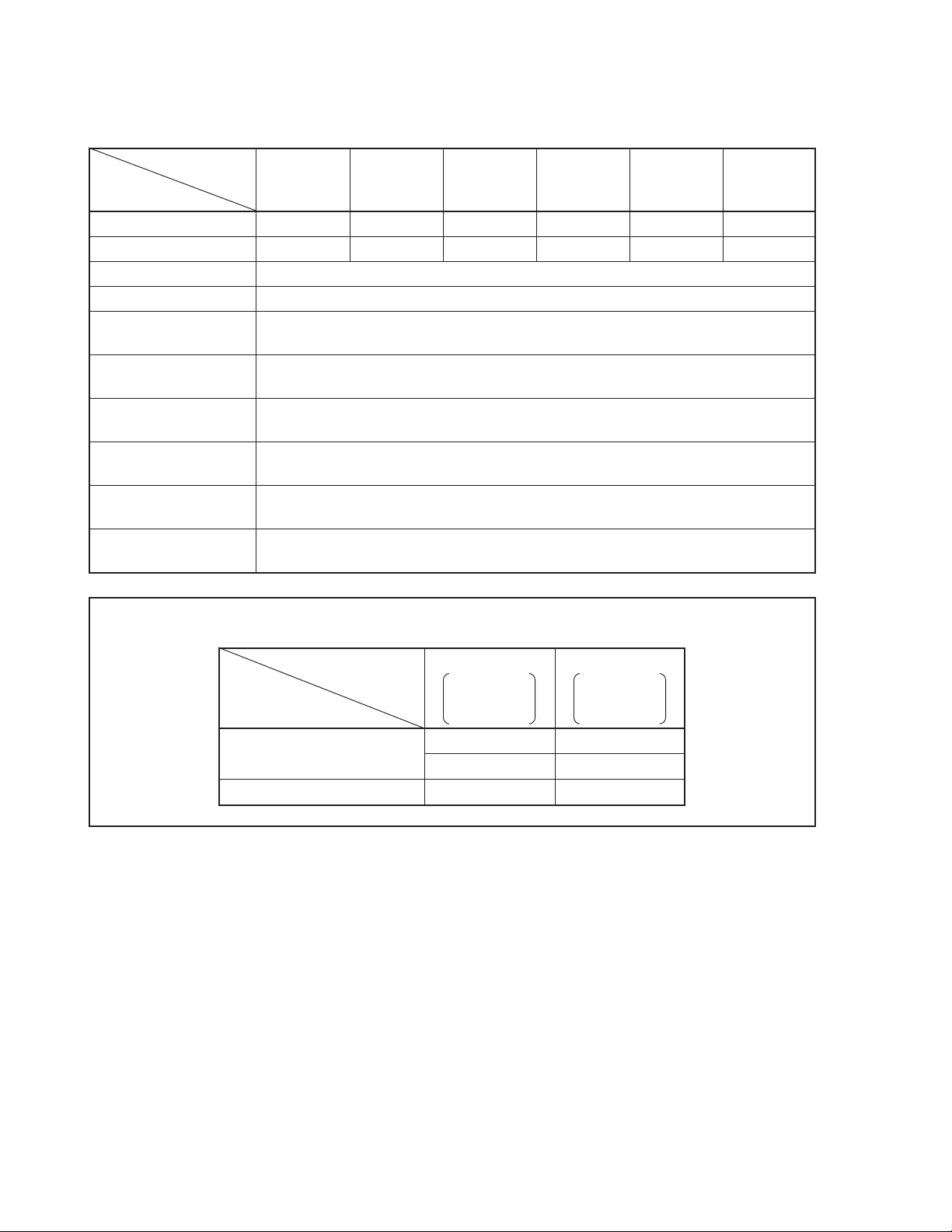
1.1 FUNCTION LIST
CHAPTER 1 GENERAL DESCRIPTION
Item
ROM configuration Mask ROM One-time PROM
ROM capacity 2KB (1024 ✕ 16 bits) 4KB (2048 ✕ 16 bits)
RAM capacity 112 ✕ 4 bits
Stack Address stack × 5, interrupt stack × 3
Number of I/O port • I/O : 20
A/D converter 8-bit resolution × 4 channels (shared with port pin), absolute precision ± 1.5 LSB or less
Timer
Serial interface 1 channel (3 wires)
AC zero cross detection Provided (can be used in application circuit at VDD = 5 V ± 10%)
function
Interrupt • Nesting by hardware (up to 3 levels)
System clock RC Ceramic RC Ceramic RC Ceramic
Instruction 8 µs2
execution time at fX = 2 MHz at fX = 8 MHz at fX = 2 MHz at fX = 8 MHz at fX = 2 MHz at fX = 8 MHz
Standby HALT, STOP
Power-on/ Available (effective only for application circuit with VDD = 5 V ± 10 %, 400 kHz to 4 MHz)
power-down reset
Supply voltage VDD = 2.7 to 5.5 V (5 V ± 10 % when using A/D converter)
Package 28-pin plastic shrink DIP, 28-pin plastic SOP
µ
PD17134A
22 • Input only : 1
• Sensor input
3 channels
• External interrupts (INT) : 1 Falling edge detection Selectable
• Internal interrupts : 1
oscillation oscillation oscillation oscillation oscillation oscillation
µ
PD17135A
Note
: 1
• 8-bit timer counter : 2 channels (16-bit timer 1 channel applicable)
• 7-bit basic interval timer : 1 channel (watchdog timer applicable)
µ
s8
µ
PD17136A
Rising edge detection
Both rising and falling edges detection
• Timer 0 (TM0)
• Timer 1 (TM1)
• Basic interval timer (BTM)
• Serial interface (SIO)
µ
s2
µ
PD17137AµPD17P136AµPD17P137A
µ
s8
µ
s2
µ
s
Note The INT pin can be used as an input pin (sense input) when the external interrupt function is not used. The
sense input function is to read the status of the pin by using the INT flag of a control register, instead of a port
register.
Caution The PROM model is highly compatible with the mask ROM model in terms of functions but its internal
ROM circuit and electrical characteristics are partially different from those of the mask ROM model.
To replace the PROM model with the mask ROM model, thoroughly evaluate the application by using
a sample of the mask ROM model.
2
Page 22

CHAPTER 1 GENERAL DESCRIPTION
1.2 ORDERING INFORMATION
Part number Package Internal ROM
µ
PD17134ACT-××× 28-pin plastic shrink DIP (400 mil) Mask ROM
µ
PD17135ACT-××× 28-pin plastic shrink DIP (400 mil) Mask ROM
µ
PD17136ACT-××× 28-pin plastic shrink DIP (400 mil) Mask ROM
µ
PD17137ACT-××× 28-pin plastic shrink DIP (400 mil) Mask ROM
µ
PD17P136ACT 28-pin plastic shrink DIP (400 mil) One-time PROM
µ
PD17P137ACT 28-pin plastic shrink DIP (400 mil) One-time PROM
µ
PD17134AGT-××× 28-pin plastic SOP (375 mil) Mask ROM
µ
PD17135AGT-××× 28-pin plastic SOP (375 mil) Mask ROM
µ
PD17136AGT-××× 28-pin plastic SOP (375 mil) Mask ROM
µ
PD17137AGT-××× 28-pin plastic SOP (375 mil) Mask ROM
µ
PD17P136AGT 28-pin plastic SOP (375 mil) One-time PROM
µ
PD17P137AGT 28-pin plastic SOP (375 mil) One-time PROM
Remark ×××: ROM code number
3
Page 23
1.3 BLOCK DIAGRAM
V
DD
P0A
0
P0A
1
P0A
2
P0A
3
P0B
0
P0B
1
P0B
2
P0B
3
P0C0/ADC
P0C1/ADC
P0C2/ADC
P0C3/ADC
P0D
P0D0/SCK
3
1
/SO
P0D
P0D
2
/TM0OUT
GND
/SI
0
1
2
3
TM0
POWER-ON/
POWER-DOWN
RESET
P0A
(CMOS)
P0B
(CMOS)
P0C
(CMOS)
A/D
Con-
verter
P0D
(N-ch)
Serial
Interface
IRQSIO
CHAPTER 1 GENERAL DESCRIPTION
Clock
divider
N
f
X
/2
RF
RAM
112 × 4 bits
SYSTEM REG.
ALU
Note1
ROM/
One-Time
PROM
Program counter
Note2
Stack
Instruction
decoder
Interrupt
controller
IRQBTM
Basic interval timer
IRQTM1
Timer 1
IRQTM0
Timer 0
System clock
generator
CPU CLOCK CLK STOP
AC
IRQTM0
ZEROCROSS
IRQTM1
detector
IRQBTM
IRQSIO
N
fX/2
N
fX/2
N
f
X
/2
P1A
(N-ch)
P1B
X
IN
Note2
(CLK)
X
OUT
INT
P1A
0
P1A
1
P1A
2
P1A
3
P1B
0
(VPP)
RESET
Remarks 1. The terms CMOS and N-ch in square brackets indicate the output form of the port.
CMOS : CMOS push-pull output
N-ch : N-channel open-drain output (Each pin can contain pull-up resistor bit-wise as specified
using a mask option.)
2. The devices in parentheses are effective only in the case of program memory write/verify mode of
µ
PD17P136A and µPD17P137A.
the
Notes 1. The ROM (or PROM) capacity of each product is as follows:
µ
1024 × 16 bits :
PD17134A, 17135A
2048 × 16 bits :µPD17136A, 17137A, 17P136A, 17P137A
2. The stack capacity of each product is as follows:
µ
5 × 10 bits :
PD17134A, 17135A
5 × 11 bits :µPD17136A, 17137A
4
Page 24
CHAPTER 1 GENERAL DESCRIPTION
1.4 PIN CONFIGURATION (TOP VIEW)
(1) Normal operating mode
28-pin plastic shrink DIP (400 mil)
µ
PD17134ACT-×××, µPD17135ACT-×××, µPD17136ACT-×××, µPD17137ACT-×××
µ
PD17P136ACT-×××, µPD17P137ACT-×××
28-pin plastic SOP (375 mil)
µ
PD17134AGT-×××, µPD17135AGT-×××, µPD17136AGT-×××, µPD17137AGT-×××
µ
PD17P136AGT-×××, µPD17P137AGT-×××
V
ADC
V
1
28
DD
P0C3/ADC
P0C2/ADC
P0C1/ADC
P0C0/ADC
P0B
P0B
P0B
P0B
P0A
P0A
P0A
P0A
3
2
1
0
3
2
1
0
3
2
1
0
GND
0 to ADC3 : Analog input for the A/D
ADC
2
3
4
5
6
7
8
9
10
11
12
13
14 15
converter
GND : Ground
INT : External interrupt input
0, OSC1 : System clock oscillation
OSC
0 to P0A3 : Port 0A
P0A
P0B0 to P0B3 : Port 0B
P0C0 to P0C3 : Port 0C
0 to P0D3 : Port 0D
P0D
P1A0 to P1A3 : Port 1A
27
26
25
24
23
22
21
20
19
18
17
16
XIN (OSC1)
OUT
(OSC0)
X
0
/SCK
P0D
1
/SO
P0D
P0D
2
/SI
P0D
3
/TM0OUT
P1A
0
P1A
1
P1A
2
P1A
3
P1B
0
RESET
INT
P1B0 : Port 1B
RESET : Reset input
SCK : Serial clock input/output
SI : Serial data input
SO : Serial data output
TM0OUT : Timer 0 carry output
ADC : Analog power supply
V
VDD : Power supply
IN, XOUT : System clock oscillation
X
5
Page 25
CHAPTER 1 GENERAL DESCRIPTION
(2) Program memory write/verify mode
28-pin plastic shrink DIP (400 mil)
µ
PD17P136ACT, 17P137ACT
28-pin plastic SOP (375 mil)
µ
PD17P136AGT, 17P137AGT
(VDD)
MD
MD
MD
MD
GND
V
1
3
2
1
0
D
7
D
6
2
3
4
5
6
7
28
27
26
25
24
23
22
DD
CLK
(Open)
(L)
D
5
D
4
D
3
D
2
D
1
D
0
8
9
10
11
12
13
21
20
19
18
17
16
14 15
V
PP
RESET
(L)
Caution ( ) represents processing of the pins which are not used in program memory write/verify
mode.
L : Connect to GND via pull-down resistor one by one.
RESET : Set the same electric potential as V
DD in program memory write/verify mode.
RESET pin is also used for system reset input before setting program memory
write/verify mode. Therefore, RESET pin should be set to the same electric
DD 10
µ
potential as V
s or later than that of VDD pin (For details, refer to CHAPTER
18 ONE-TIME PROM WRITING/VERIFYING).
Open : Do not connect anything.
DD : Connect to VDD directly.
V
6
Page 26

CHAPTER 1 GENERAL DESCRIPTION
CLK : Clock input for address updating
D0-D7 : Data input/output
GND : Ground
0-MD3 : Operation mode select
MD
RESET : Reset input
DD : Power supply
V
VPP : Program voltage application
7
Page 27

[MEMO]
8
Page 28

CHAPTER 2 PIN FUNCTIONS
2.1 PIN FUNCTIONS
Pin No. Pin name Function Output At reset
1VADC Supplies power and reference voltage for the A/D converter — —
Note1
Note1
Note1
Note1
Note1
Constitute port 0C, serve as analog input pins of A/D CMOS Input
Note1
is written or verified.
P0C3 to P0C0
•
• 4-bit input/output port
• Input/output setting in 1-bit unit
ADC3 to ADC0
•
• Analog input for the A/D converter
MD3 to MD0
•
• Available for the µPD17P136A and µPD17P137A only
• Selects operating mode at program memory writing/
verification
Used as port 0B, or data input/output pins in program CMOS Input
P0B3 to P0B0
•
• 4-bit input/output port
• Input/output setting in 4-bit unit
• Software-selectable pull-up resistor
D7 to D4
•
• Available for the µPD17P136A and µPD17P137A only
• 8-bit data input/output at program memory writing/
verification
Used as port 0A, or data input/output pin in program memory CMOS Input
P0A3 to P0A0
•
• 4-bit input/output port
• Input/output setting in 4-bit unit
• Software-selectable pull-up resistor
D3 to D0
•
• Available for the µPD17P136A and µPD17P137A only
• 8-bit data input/output at program memory writing/
verification
A pull-up resistor can be internally connected by mask
Note2
option
2 P0C3/ADC3/MD3
| | converter, or select operating mode when program memory push-pull (P0C)
5 P0C0/ADC0/MD0
6 P0B3/D7
| | memory write/verify mode. push-pull (P0B)
9 P0B0/D4
10 P0A3/D3
| | write/verify mode. push-pull (P0A)
13 P0A0/D0
14 GND Ground — —
15 INT External interrupt request input or sensor signal input — Input
16 RESET System reset input pin — Input
Notes 1. The MD0-MD3 and D0-D7 pins are valid with the µPD17P136A and 17P137A only.
2. The µPD17P136A and 17P137A do not have a pull-up resistor connected by mask option.
9
Page 29
CHAPTER 2 PIN FUNCTIONS
Pin No. Pin name Function Output At reset
17 P1B0/VPP
18 P1A3 Port 1A N-ch open Input
| | • 4-bit input/output port drain
21 P1A0 • Input/output setting in 4-bit unit
22 P0D3/TM0OUT Used as port 0D, or timer 0 carry output, serial data input, N-ch open Input
23 P0D 2/SI
24 P0D1/SO
25 P0D0/SCK
26 XOUT In the case of the µPD17135A/17137A/17P137A — —
27 XIN/CLK
26 OSC0 In the case of the µPD17134A/17136A/17P136A
27 OSC1/CLK
28 VDD Power supply — —
Note1
Note3
Note3
Used as port 1B, or programming voltage supply pin in Input Input
program memory write/verify mode.
P1B0
•
• 1-bit input port
• A pull-up resistor can be internally connected by mask
VPP
•
• Available for the µPD17P136A and µPD17P137A only
• Applies programming voltage (+12.5 V) at program
• A pull-up resistor can be internally connected by mask
serial data output, and serial clock input/output pins drain
A pull-up resistor can be internally connected by mask
option
P0D3 to P0D0
•
• 4-bit input/output port
• Input/output setting in 1 bit unit
TM0OUT
•
• Timer 0 carry output
SI
•
• Serial data input
SO
•
• Serial data output
SCK
•
• Serial clock input/output
XIN, XOUT
•
• Connected to a resonator for system clock oscillation
• The ceramic resonator is connected.
CLK
•
• Available for the µPD17P137A only
• Clock input pin for address updating at program
OSC0, OSC1
•
• Connected to a resonator for system clock oscillation
• Resistor is connected between OSC0 and OSC1.
CLK
•
• Available for the µPD17P136A only
• Clock input pin for address updating at program
In the program memory write/verify mode of the
µ
PD17P136A/17P137A, +6 V is applied.
Note2
option
memory writing/verification
Note2
option
Note2
memory writing/verification
memory writing/verification
Notes 1. The VPP pin is valid only with the µPD17P136A and 17P137A.
µ
2. The
PD17P136A and 17P137A do not have a pull-up resistor connected by mask option.
3. The CLK pin is valid only with the µPD17P136A and 17P137A.
10
Page 30
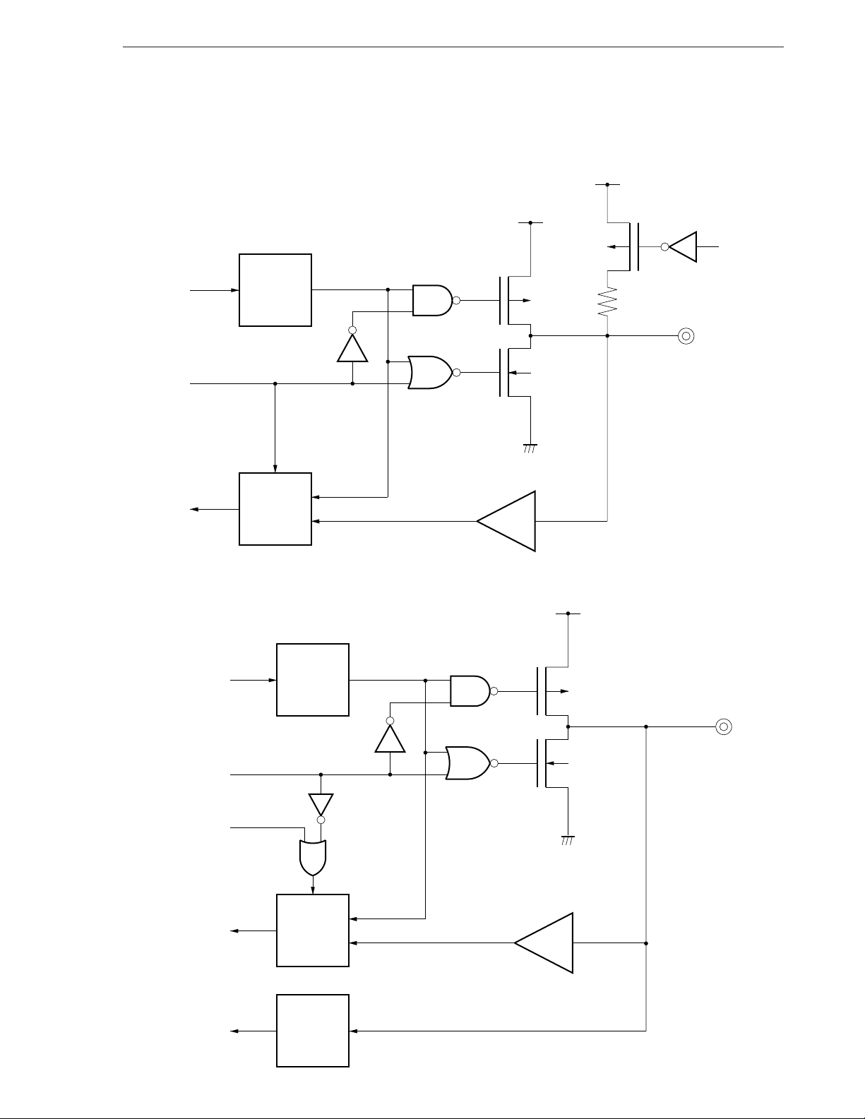
CHAPTER 2 PIN FUNCTIONS
2.2 PIN INPUT/OUTPUT CIRCUIT
Below are simplified diagrams of the input/output circuits for each pin.
(1) P0A
0-P0A3, P0B0-P0B3
1
2
V
DD
Data
Output
disable
(2) P0C0/ADC0 - P0C3/ADC3
Output
latch
Selector
V
Input buffer
DD
P-ch
Pull-up
flag
4
5
3
P-ch
6
N-ch
7
8
9
10
11
V
DD
12
Data
Output
disable
Input
disable
Output
latch
Selector
A/D
converter
Input buffer
P-ch
N-ch
13
14
15
16
17
18
19
20
11
Page 31

(3) P0D0-P0D3, P1A0-P1A3
CHAPTER 2 PIN FUNCTIONS
V
DD
Data
Output
latch
Output
N-ch
disable
Selector
Input buffer
Note The µPD17P136A and 17P137A do not have a pull-up resistor as mask option.
(4) P1B
0
V
DD
Mask option
Note
Mask option
Input buffer
Note The µPD17P136A and 17P137A do not have a pull-up resistor as mask option.
Note
12
Page 32

(5) INT
CHAPTER 2 PIN FUNCTIONS
1
2
(6) RESET
Note The
Input buffer
V
DD
Mask option
Input buffer
µ
PD17P136A and 17P137A do not have a pull-up resistor as mask option.
3
4
5
6
7
Note
8
9
10
11
12
13
14
15
16
17
18
19
20
13
Page 33

CHAPTER 2 PIN FUNCTIONS
2.3 PROCESSING OF UNUSED PINS
The unused pins should be handled as follows:
Table 2-1. Processing of Unused Pins
Pin Name Recommended Processing
Internal External
Port Input mode P0A, P0B Connect pull-up resistor by software Open
P0C — Connect each pin to VDD or GND via
P0D, P1A Pull-up resistor not connected by mask Directly connect to GND
option
Pull-up resistor connected by mask Open
option
Note2
P1B0
Output mode P0A, P0B, P0C — Open
(CMOS port)
P0D, P1A Outputs low level without pull-up
(N-ch open- resistor connected by mask option
drain ports) Outputs high level without pull-up
External interrupt (INT) Pull-up resistor not connected by mask Directly connect to VDD or GND
Note3
RESET
when only internal power-ON/power-
down reset function is used Pull-up resistor connected by mask
VADC — Directly connect to VDD
Pull-up resistor not connected by mask Directly connect to GND
option
resistor connected by mask option
option
Pull-up resistor connected by mask Open
option
Pull-up resistor not connected by mask Directly connect to VDD
option
option
resistor
Note 1
Notes 1. When connecting an external pull-up resistor (to VDD via resistor) or pull-down resistor (to GND via
resistor), make sure that the driving voltage and current consumption of the port are not exceeded. When
connecting a pull-up or pull-down resistor with a high resistance to a port pin, make sure that noise is not
superimposed on the pin. Generally, the resistance of the pull-up or pull-down resistor is about several
kΩ, though it varies depending on the application circuit.
2. Because the P1B
0 pin is multiplexed with a test mode setting function, do not connect a pull-up resistor
to this pin using the mask option. Directly connect it to GND.
3. In an application circuit where high reliability is required, be sure to input the RESET signal from an external
source. Because the RESET pin is multiplexed with a mode setting function, directly connect it to V
if not use.
Caution It is recommended that the I/O mode, pull-up of resistors by software, and output levels of pins be
fixed by repeatedly setting in each loop of the program.
µ
Remark The
PD17P136A and 17P137A do not have a pull-up resistor as mask option.
14
DD
Page 34

CHAPTER 2 PIN FUNCTIONS
2.4 NOTES ON USING RESET PIN AND P1B0 PIN
The RESET and P1B
subseries are tested (for IC test), in addition to the functions described in 2.1 PIN FUNCTIONS.
When a voltage exceeding VDD is applied to either of these pins, the test mode is set. This means that, even during
the normal operation, the test mode is set if a noise exceeding V
performed normally.
This is especially true if the wiring length of the RESET or P1B0 pin is too long in which case a noise may be
superimposed on the wiring.
Therefore, perform wiring so that noise may not be superimposed, by keeping the wiring length as short as possible.
If noise is inevitable, take noise preventive measures by using an external component as illustrated below.
0 pins have a function for setting a test mode in which the internal operations of the
DD is applied. As a result, the operation may not be
µ
PD17134A
1
2
3
4
5
• Connect a diode with low VF between
DD and RESET/P1B0
V
V
DD
V
Diode with
low V
F
RESET, P1B
DD
0
• Connect a capacitor between
VDD and RESET/P1B0
V
DD
V
DD
RESET, P1B
0
6
7
8
9
10
11
12
13
14
15
15
16
17
18
19
20
Page 35

[MEMO]
16
Page 36

CHAPTER 3 PROGRAM COUNTER (PC)
The program counter is used to specify an address in program memory.
3.1 PROGRAM COUNTER CONFIGURATION
Figure 3-1 shows the configuration of the program counter.
µ
The program counters of the
The program counters of the µPD17136A, µPD17137A, µPD17P136A, and µPD17P137A are 11-bit binary
counters.
This program counter is incremented whenever an instruction is executed.
PD17134A and µPD17135A are 10-bit binary counters.
Figure 3-1. Program Counter
MSB
PC10
PC9 PC8 PC7 PC6 PC5 PC4 PC3 PC2 PC1 PC0
PC
Remark The shaded part is effective only in the case of
µ
PD17136A/17137A/17P136A/17P137A.
LSB
3.2 PROGRAM COUNTER OPERATION
Normally, the program counter is automatically incremented each time a command is executed. The memory
address at which the next instruction to be executed is stored is assigned to the program counter under the following
conditions: At reset; when a branch, subroutine call, return, or table reference instruction is executed; or when an
interrupt is received.
3.2.1 to 3.2.7 explain program counter operation during execution of each instruction.
17
Page 37

CHAPTER 3 PROGRAM COUNTER (PC)
Figure 3-2. Value of the Program Counter after Instruction Execution
Program counter
Instruction
BR addr
CALL addr
BR @AR
CALL @AR
(MOVT DBF, @AR)
RET
RETSK
RETI
During interrupt
bit
PC9 PC8 PC7 PC6 PC5 PC4 PC3 PC2 PC1 PC0
PC10
0000000000At reset
0
Value set by the addr
Value in the address register (AR)
Value in the address stack register location pointed to by the stack pointer
(return address)
Vector address for the interrupt
Program counter value
Remark The shaded part is effective only in the case of µPD17136A/17137A/17P136A/17P137A.
3.2.1 At Reset
By setting the RESET pin to low, the program counter is set to 0000H.
Figure 3-3. Value in the Program Counter after Reset
MSB
0
0
0 00000000
All bits are set to 0
Remark The shaded part is effective only in the case of
µ
PD17136A/17137A/17P136A/17P137A.
LSB
3.2.2 During Execution of the Branch Instruction (BR)
There are two ways to specify branching using the branch instruction. One is to specify the branch address in the
operand using the direct branch instruction (BR addr). The other is branch to the address specified by the address
register using the indirect branch instruction (BR @AR).
The address specified by a BR addr instruction is placed in the program counter.
Figure 3-4. Value in the Program Counter during Execution of a BR addr Instruction
MSB
PC10
PC8 PC7 PC6 PC5 PC4 PC3 PC2 PC1 PC0
PC9
LSB
Value specified in the direct branch instruction
Remark The shaded part is effective only in the case of
18
µ
PD17136A/17137A/17P136A/17P137A.
Page 38

CHAPTER 3 PROGRAM COUNTER (PC)
An indirect branch instruction causes the address in the address counter to be placed in the program counter.
Figure 3-5. Value in the Program Counter during Execution of a BR @AR Instruction
MSB
PC10 PC8 PC7 PC6 PC5 PC4 PC3 PC2 PC1 PC0
PC9
AR10 AR8 AR7 AR6 AR5 AR4 AR3 AR2 AR1 AR0
AR9
Remark The shaded part is effective only in the case of
µ
PD17136A/17137A/17P136A/17P137A.
LSB
3.2.3 During Execution of Subroutine Calls (CALL)
There are two ways to specify branching using subroutine calls. One is to specify the branch address in the operand
using the direct subroutine call (CALL addr). The other is branch to the address specified by the address register
using the indirect subroutine call (CALL @AR).
A CALL addr causes the value in the program counter to be saved in the stack and then the address specified in
µ
the operand to be placed in the program counter. CALL addr can specify 000H-03FFH in the
PD17134A and 17135A,
and 0000H-07FFH in the µPD17136A, 17137A, 17P136A, and 17P137A.
Figure 3-6. Value in the Program Counter during Execution of a CALL addr
MSB
PC10
PC9 PC8 PC7 PC6 PC5 PC4 PC3 PC2 PC1 PC0
Address specified in the addr
Remark The shaded part is effective only in the case of
µ
PD17136A/17137A/17P136A/17P137A.
LSB
A CALL @AR causes the value in the program counter to be saved in the stack and then the value in the address
register to be placed in the program counter.
19
Page 39

CHAPTER 3 PROGRAM COUNTER (PC)
Figure 3-7. Value in the Program Counter during Execution of an Indirect Subroutine Call
MSB
PC10
AR10
Address stack register n
PC9 PC8 PC7 PC6 PC5 PC4 PC3 PC2 PC1 PC0
AR9 AR8 AR7 AR6 AR5 AR4 AR3 AR2 AR1 AR0
(n = 0 to 4)
LSB
Remark The shaded part is effective only in the case of µPD17136A/17137A/17P136A/17P137A.
3.2.4 During Execution of Return Instructions (RET, RETSK, RETI)
During execution of a return instruction (RET, RETSK, RETI), the program counter is restored to the value saved
in the address stack register.
Figure 3-8. Value in the Program Counter during Execution of a Return Instruction
MSB
LSB
PC10
Remark The shaded part is effective only in the case of
PC9 PC8 PC7 PC6 PC5 PC4 PC3 PC2 PC1 PC0
Address stack register n
µ
PD17136A/17137A/17P136A/17P137A.
(n = 0 to 4)
3.2.5 During Table Reference (MOVT)
During execution of table reference (MOVT DBF, @AR), the value in the program counter is saved in the stack,
the address register is set by the program counter, then the contents stored at that program memory location is read
into the data buffer (DBF). After that, the program counter is restored to the value saved in the address stack register.
One level of the address stack is temporarily used during execution of table reference. Be careful of the stack level.
20
Page 40

CHAPTER 3 PROGRAM COUNTER (PC)
3.2.6 During Execution of Skip Instructions (SKE, SKGE, SKLT, SKNE, SKT, SKF)
When skip conditions are met and a skip instruction (SKE, SKGE, SKLT, SKNE, SKT, SKF) is executed, the
instruction immediately following the skip instruction is treated as a no operation instruction (NOP). Therefore, whether
skip conditions are met or not, the number of instructions executed and instruction execution time remain the same.
3.2.7 When an Interrupt Is Received
When an interrupt is received, the value in the program counter is saved in the address stack. Next, the vector
address for the interrupt received is placed in the program counter.
21
Page 41

[MEMO]
22
Page 42

CHAPTER 4 PROGRAM MEMORY (ROM)
The program organization of the µPD17134A subseries is shown in Table 4-1.
Table 4-1. Program Memory Configuration
Product name Program memory capacity Program memory address
µ
PD17134A 2K bytes (1024 × 16 bits) 0000H-03FFH
µ
PD17135A
µ
PD17136A
µ
PD17137A 4K bytes (2048 × 16 bits) 0000H-07FFH
µ
PD17P136A
µ
PD17P137A
Program memory stores the program and the constant data table. The first area of the program memory is assigned
to reset start and interrupt vector addresses.
The program memory address is specified by the program counter.
4.1 PROGRAM MEMORY CONFIGURATION
Figure 4-1 shows the program memory map. Branch instructions, subroutine calls, and table references can specify
any address in program memory.
µ
Figure 4-1. Program Memory Map for the
Address
0000H
0001H
0002H
0003H
0004H
0005H
Serial interface interrupt vector
Basic interval timer interrupt vector
Timer 1 interrupt vector
Timer 0 interrupt vector
External (INT) interrupt vector
16 bits
Reset start address
PD17134A Subseries
Subroutine entry
address for the CALL
addr instruction
Branch address for
the BR addr instruction
Branch address for
the BR @AR instruction
Subroutine entry
address for the CALL
@AR instruction
03FFH
07FFH
m
( PD17134A/17135A)
m
( PD17136A/17137A/17P136A/17P137A)
Table reference address
for the MOVT DBF, @AR
instruction
23
Page 43

CHAPTER 4 PROGRAM MEMORY (ROM)
4.2 PROGRAM MEMORY USAGE
Program memory has the following two main functions:
(1) Storage of the program
(2) Storage of constant data
The program is made up of the instructions which operate the CPU (Central Processing Unit). The CPU executes
sequential processing according to the instructions stored in the program. In other words, the CPU reads each
instruction in the order stored by the program in program memory and executes it.
Since all instructions are 16-bit long words, each instruction is stored in a single address in program memory.
Constant data, such as display patterns, are set beforehand. The MOVT is used for reading constant data in
program memory to transfer data from program memory to the data buffer (DBF) in data memory. Reading the constant
data in program memory is called table reference.
Program memory is read-only (ROM: Read Only Memory) and therefore cannot be changed by any instructions.
4.2.1 Flow of the Program
The program is usually stored in program memory starting from address 0000H and executed sequentially one
address at a time. However, if for some reason a different kind of program is to be executed, it will be necessary to
change the flow of the program. In this case, the branch instruction (BR instruction) is used.
If the same program code is going to appear in a number of places, reproducing the code each time it needs to
be used will decrease the efficiency of the program. In this case, the program should be stored in only one place in
memory. Then, by using the CALL instruction, call the same program. Such a program is called a subroutine. As
opposed to a subroutine, code used during normal operation is called the main routine.
For cases completely unrelated to the flow of the program (in which a section of code is to be executed when a
certain condition arises), the interrupt function is used. Whenever a condition arises that is unrelated to the flow of
the program, the interrupt function can be used to branch the program to a prechosen memory location (called a vector
address).
Items (1) to (5) explain branching of the program using the interrupt function and instructions.
(1) Vector address
Table 4-2 shows the address to which the program is branched (vector address) when a reset or interrupt
occurs.
24
µ
Table 4-2. Vector Address for the
Vector address Cause of the interrupt
0000H Reset
0001H Serial interface interrupt
0002H Basic interval timer interrupt
0003H Timer 1 interrupt
0004H Timer 0 interrupt
0005H External (INT) interrupt
PD17134A Subseries
Page 44

CHAPTER 4 PROGRAM MEMORY (ROM)
(2) Direct branch
A direct branch (BR addr) instruction branches a value of operand (addr) as an address. (In the case of the
µ
PD17134A and µPD17135A, the most significant bit must be 0. If an address is specified outside of this range,
an error will occur in the assembler.) A BR addr instruction can be used to branch to any address in program
memory.
(3) Indirect branch
When executing an indirect branch (BR @AR), the program branches to the address specified by the value
stored in the address register (AR). A BR @AR can be used to branch to any address in program memory.
Also see 7.2 ADDRESS REGISTER (AR).
(4) Subroutine
To branch execution to a subroutine, the subroutine call (CALL) instruction is used.
The CALL instruction can be used in two ways: as a direct subroutine call instruction (CALL addr) that causes
execution to branch using the value of the operand (addr) as an address, and as an indirect subroutine call
instruction (CALL @AR) that causes execution to branch using the contents of an address register as an
address.
To return from a subroutine, the RET or RETSK instruction is used. By executing the RET or RETSK instruction,
execution is returned to the program memory address next to the one at which the CALL instruction was
executed.
When the RETSK instruction is used, the first instruction after execution has returned from the subroutine is
executed as a NOP instruction.
25
Page 45

CHAPTER 4 PROGRAM MEMORY (ROM)
<1> Direct subroutine call
When using a direct subroutine call (CALL addr), the 11-bit instruction operand is used to specify a
µ
program memory address of the branched subroutine. (In the case of the
PD17134A and µPD17135A,
the most significant bit must be 0. If an address is specified outside of this range, an error will occur
in the assembler.)
Example
Figure 4-2. CALL addr Instruction
Address
0000H
SUB1;
RET
Note
07FFH
Note The program memory of the
Program memory
CALL SUB1
µ
PD17134A and µPD17135A is address 0000H to 03FFH.
26
<2> Indirect subroutine call
When using an indirect subroutine call (CALL @AR), the value in the address register (AR) should be
an address of the called subroutine. This instruction can be used to branch any address in program
memory.
Also see 7.2 ADDRESS REGISTER (AR).
Page 46

CHAPTER 4 PROGRAM MEMORY (ROM)
4.2.2 Table Reference
Table reference is used to reference constant data in program memory.
The table reference instruction (MOVT DBF, @AR) is used to store the contents of the program memory address
specified by the address register in the data buffer.
Since each location in program memory contains 16 bits of information, the MOVT instruction causes
16 bits of data to be stored in the data buffer. The address register can be used to table reference any location
in program memory.
Caution Note that one level of the address stack is temporarily used when performing table reference.
Be sure not to exceed the stack level that can be used. Also see 7.2 ADDRESS REGISTER (AR)
and CHAPTER 10 DATA BUFFER (DBF).
Remark Two instruction cycles are required to execute the table reference instruction, but this is an exception.
Figure 4-3. Table Reference (MOVT DBF, @AR)
Data buffer
DBF3
3
DBF2 DBF1 DBF0
b0b1b2b
3
b0b1b2b
3
b0b1b2b
16-bit data read
Address register
AR3 AR2 AR1 AR0
Note
b0b1b2b
3
b0b1b2b
3
3
b0b1b2b
00000
Table address specification
Program memory
b
15
3
3
b0b1b2b
b0b1b2b
b14b13b12b11b
10
9
3
b4b5b6b7b8b
b0b1b2b
Constant data
Note This bit is fixed to 0 in the case of the
µ
PD17134A and µPD17135A.
27
Page 47

CHAPTER 4 PROGRAM MEMORY (ROM)
(1) Constant data table
Example 1 shows an example of code used to reference a constant data table.
Example 1. Program to read data in a constant data table.
OFFSET MEM 0.00H ; Area to store the offset address.
ROMREF:
BANK0
; Stores the start address of the constant data
; table in the AR register.
MOV AR3, #.DL.TABLE SHR 12 AND 0FH
MOV AR2, #.DL.TABLE SHR 8 AND 0FH
MOV AR1, #.DL.TABLE SHR 4 AND 0FH
MOV AR0, #.DL.TABLE AND 0FH
MOV RPH, #0 ; Sets the register pointer to row address 7.
MOV RPL, #7 SHL 1 ;
ADD AR0, OFFSET ; Adds the offset address.
ADDC AR1, #0
ADDC AR2, #0
ADDC AR3, #0
MOVT DBF, @AR ; Reads the constant data.
TABLE:
DW 0001H ; When OFFSET = 0H
DW 0002H
DW 0004H
DW 0008H
DW 0010H
DW 0020H
DW 0040H
DW 0080H
DW 0100H
DW 0200H
DW 0400H
DW 0800H
DW 1000H
DW 2000H
DW 4000H
DW 8000H ; When OFFSET = 0FH
END
28
Page 48

CHAPTER 4 PROGRAM MEMORY (ROM)
(2) Branch address table
Example 2 shows an example of code used to reference a branch address table.
Example 2. Program to branch to the address of the branch address table.
OFFSET MEM 0.00H ; Area to store the offset address.
ROMREF:
BANK0 ; Stores the start address of the constant data
; table in the AR register.
MOV AR3, #.DL.TABLE SHR 12 AND 0FH
MOV AR2, #.DL.TABLE SHR 8 AND 0FH
MOV AR1, #.DL.TABLE SHR 4 AND 0FH
MOV AR0, #.DL.TABLE AND 0FH
MOV RPH, #0 ; Sets the register pointer to row address 7.
MOV RPL, #7 SHL 1
ADD AR0, OFFSET ; Adds the offset address.
ADDC AR1, #0
MOVT DBF, @AR ; Reads the branch address
PUT AR, DBF ; AR ← Branch address
BR @AR
TABLE:
DW 0001H ; When OFFSET = 0H
DW 0002H
DW 0004H
DW 0008H
DW 0010H
DW 0020H
DW 0040H
DW 0080H
DW 0100H
DW 0200H ; When OFFSET = 9H
END
29
Page 49

[MEMO]
30
Page 50

CHAPTER 5 DATA MEMORY (RAM)
Data memory stores data such as operation and control data. Data can be read from or written to data memory
with an instruction during normal operation.
5.1 DATA MEMORY CONFIGURATION
Figure 5-1 shows the configuration of data memory.
Data memory is divided into two areas called banks: BANK0 and BANK1.
An address is allocated to the data memory for each bank. An address consists of 4 bits of memory called “a nibble”.
The address of data memory consists of 7 bits. The high-order 3 bits are called “the row address”, and the loworder 4 bits are called “the column address”. For example, when the address of data memory is 1AH (0011010B),
the row address is 1H (001B), and the column address is AH (1010B).
5.1.1 to 5.1.6 describe functions of data memory other than its use as address space.
Figure 5-1. Data Memory Configuration
BANK0
0123456789ABCDEF
0
1
2
3
4
Row address
5
6
P0A
7
(4 bits)
BANK1
0123456789ABCDEF
0
1
2
3
4
5
6
P1A
7
(4 bits)
P0B
(4 bits)
P1B
(4 bits)
P0C
(4 bits)
Fixed
to 0
P0D
(4 bits)
Fixed
to 0
Column address
Unmounted
System register
System register
DBF3 DBF2 DBF1 DBF0
Example
Address 1AH
of BANK0
The same system register is
allocated in each bank.
Caution No hardware is assigned to addresses 00H through 6FH in BANK1. Do not use this area. If the
contents of this area are read, the value is undefined. An instruction to write data to this area
is invalid.
31
Page 51

CHAPTER 5 DATA MEMORY (RAM)
5.1.1 System Register (SYSREG)
The system register (SYSREG) consists of the 12 nibbles allocated at addresses 74H to 7FH in data memory. The
system register (SYSREG) is allocated independently of the banks. This means that each bank has the same system
register at addresses 74H to 7FH.
Figure 5-2 shows the configuration of the system register.
For details, refer to CHAPTER 7 SYSTEM REGISTER (SYSREG).
Figure 5-2. System Register Configuration
System register (SYSREG)
74H 75H 76H 77H 78H 79H 7AH 7BH 7CH 7DH 7EH 7FHAddress
Program
status
word
(PSWORD)
Name
(Symbol)
Address register
(AR)
Window
register
(WR)
Bank
register
(BANK)
Index register (IX)
Data memory
row address
pointer (MP)
General
register
pointer
(RP)
5.1.2 Data Buffer (DBF)
The data buffer consists of four nibbles allocated at addresses 0CH to 0FH in BANK0 of data memory.
Figure 5-3 shows the configuration of the data buffer.
Figure 5-3. Data Buffer Configuration
Data buffer (DBF)
Address
Symbol
0CH
DBF3
0DH
DBF2
0EH
DBF1
0FH
DBF0
32
Page 52

CHAPTER 5 DATA MEMORY (RAM)
5.1.3 General Register (GR)
The general register consists of 16 nibbles specified by an arbitrary row address in an arbitrary bank in data memory.
This arbitrary row address in an arbitrary bank is specified by the register pointer (RP) in the system register
(SYSREG).
Figure 5-4 shows the configuration of the general register (GR).
Figure 5-4. General Register (GR) Configuration
Column address BANK0
0123456789ABCDEF
0
1
2
3
4
Row address
5
6
Port register
7
BANK1
0
1
2
3
4
5
6
Port register
7
Unmounted
SYSREG
SYSREG
General register
Area specifiable as general register
Pointed to by general register
pointer (RP) in system register.
Note that row addresses 0 to 6
of BANK1 are unmounted memory locations. The register
pointer (RP) should therefore
not specify a row address in this
area.
The same register is allocated
for each bank.
5.1.4 Port Registers
A port register consists of eight nibbles allocated at addresses 70H to 73H in each bank of the data memory.
As shown in Figure 5-5, the high-order 3 bits of address 71H of BANK1 and all of addresses 72H and 73H of BANK1
are always set to 0.
Figure 5-5 shows the configuration of the port registers.
Address
BANK0
Symbol
BANK1
Figure 5-5. Port Register Configuration
Port register
70H
P0A
P
P
P
P
0
0
0
0
A
A
A
A
0
1
2
3
P1A P1B
P
P
P
P
1
1
1
1
A
A
A
A
3
2
1
0
71H
P0B
P
P
P
P
P
P
0
0
0
0
0
0
C
C
B
B
B
B
2
3
0
1
2
3
P
Fixed to “0” Fixed to “0” Fixed to “0”
1
B
0
72H
P0C
73H
P0D
P
P
P
P
P
P
0
0
0
0
0
0
D
D
D
D
C
C
0
1
2
3
0
1
33
Page 53

CHAPTER 5 DATA MEMORY (RAM)
5.1.5 General Data Memory
General data memory is all the data memory not used by the port and system registers (SYSREG). In other words,
general data memory consists of 112 nibbles in BANK0.
5.1.6 Unmounted Data Memory
There is no hardware mounted at addresses 00H to 6FH of BANK1. Any attempt to read this area will yield undefined
value. Writing data to this area is invalid and should therefore not be attempted.
34
Page 54

CHAPTER 6 STACK
The stack is a register used to save information such as the program return address and the contents of the system
register during execution of subroutine calls or interrupts.
6.1 STACK CONFIGURATION
Figure 6-1 shows the stack configuration.
µ
The stack consists of the following parts: one 3-bit binary counter stack pointer, five 10-bit (
11-bit (µPD17136A, 17137A, 17P136A, 17P137A) address stack registers, and three 6-bit interrupt stack registers.
Figure 6-1. Stack Configuration
PD17134A, 17135A)/
Stack pointer
(SP)
b
2
b
1
SPb2SPb1SPb
SP is initialized to
5H at reset
b
9
b
b
0
0
0H
10
b8b7b6b5b4b3b2b
1H
2H
3H
4H
Address stack register
Address stack register 0
Address stack register 1
Address stack register 2
Address stack register 3
Address stack register 4
Interrupt stack register
BANKSK0 BCDSK0
0H
BANKSK1 BCDSK1
1H
BANKSK2 BCDSK2
2H
CMPSK0 CYSK0
CMPSK1 CYSK1
CMPSK2 CYSK2
Remark The shaded part is effective only in the case of µPD17136A/17137A/17P136A/17P137A.
6.2 FUNCTIONS OF THE STACK
b
0
1
IXESK0ZSK0
IXESK1ZSK1
IXESK2ZSK2
The stack is used to save the return address during execution of subroutine calls and table reference instructions.
When an interrupt occurs, the program return address, bank register (BANK), and the program status word (PSWORD)
are automatically saved in the stack.
35
Page 55

CHAPTER 6 STACK
6.3 ADDRESS STACK REGISTERS (ASRs)
Five 11-bit address stack registers (ASRs) are provided as shown in Figure 6-1. The functions of these registers
are as follows:
• Store a return address when the CALL addr or CALL @AR instruction is executed, when the first instruction
cycle of the “MOVT DBF, @AR” instruction is executed, or when an interrupt is accepted.
• Store the contents of an address register (AR) when the PUSH AR instruction is executed. The ASR to which
the data is to be stored is specified by decrementing the value of the stack pointer (SP) by one when the
instruction is executed.
• Restore the contents of the ASR (return address) specified by the stack pointer to the program counter and
increment the value of the stack pointer by one when the RET or RETSK instruction is executed, when the second
instruction cycle of the “MOVT DBF, @AR” instruction is executed, or when the RETI instruction is executed.
• Transfer the value of the ASR specified by the stack pointer to an address register and decrement the value
of the stack pointer by one when the POP AR instruction is executed.
Caution If the stack pointer underflows as a result of executing the CALL addr or CALL @AR instruction
or servicing an interrupt, it is assumed that a hang-up occurs. Consequently, the internal reset
signal is generated, the hardware is initialized, and the program is started from address 0000H.
µ
Remark The size of the ASR differs depending on the model. The
ASRs, while the µPD17136A, 17137A, 17P136A, and 17P137A have five 11-bit ASRs.
6.4 INTERRUPT STACK REGISTERS (INTSKs)
Three 5-bit interrupt stack registers (INTSKs) are provided as shown in Figure 6-1. The functions of these registers
are as follows:
• Five flags (BCD, CMP, CY, Z, and IXE) in the program status word (PSWORD) in the system register (SYSREG)
to be explained shortly are saved to the INTSK when an interrupt occurs. After the flags have been saved, all
the bits of the BANK and PSWORD are cleared to 0.
• The contents of INTSK are restored to the PSWORD when the RETI instruction is executed.
• INTSK saves data each time an interrupt has been accepted.
Caution If interrupts are accepted exceeding 3 levels, the first data is lost.
PD17134A and 17135A have five 10-bit
36
Page 56

CHAPTER 6 STACK
6.5 STACK POINTER (SP) AND INTERRUPT STACK REGISTERS
The stack pointer is a 3-bit binary counter that specifies the addresses of the five address stack registers as shown
in Figure 6-1, and is assigned to address 01H of the register file. The value of the stack pointer is initialized to 5H
at reset.
• The value of SP is decremented by one when the CALL addr or CALL @AR instruction is executed, when the
first instruction cycle of the “MOVT DBF, @AR” instruction is executed, or when an interrupt is accepted.
• The value of SP is incremented by one when the RET or RETSK instruction is executed, when the second
instruction cycle of the “MOVT DBF, @AR” instruction is executed, when the POP AR instruction is executed,
or when the RETI instruction is executed.
When an interrupt is accepted, the counter of the interrupt stack registers is also decremented by one in addition
to the SP. The value of the counter of the interrupt stack registers is incremented by one only when the RETI instruction
is executed.
Table 6-1. Operation of Stack Pointer
Instruction Value of stack pointer (SP) Counter of interrupt stack registers
CALL addr
CALL @AR
MOVT, DBF @AR (1st instruction cycle)
PUSH AR
RET
RETSK
MOVT DBF, @AR (2nd instruction cycle)
POP AR
Accepting interrupt –1 –1
RETI +1 +1
–1
Not affected
+1
Remark Two instruction cycles are required to execute the “MOVT DBF, @AR” instruction, but this is an
exception.
Because the stack pointer (SP) is a 3-bit binary counter, it can take a value 0H to 7H. If the value of the stack pointer
is 6 or more, however, an internal reset signal is generated (to prevent a hang-up). This is because only five address
stack registers are available.
Because the stack pointer is located on the register file, its value can be directly read by manipulating the register
file with the POKE instruction. The value of the stack pointer is also changed at this time, but the values of the address
stack registers are not affected. Of course, the stack pointer can also be read by using the PEEK instruction.
The value of the stack pointer is 5H at reset.
37
Page 57

CHAPTER 6 STACK
6.6 STACK OPERATION
Stack operation during execution of each instruction is explained in 6.6.1 to 6.6.3.
6.6.1 On Execution of Instructions CALL, RET, RETSK
Table 6-2 shows operation of the stack pointer (SP), address stack register, and the program counter (PC) during
execution of CALL, RET, and RETSK.
Table 6-2. Operation of the Instructions CALL, RET, and RETSK
Instruction Operation
CALL addr (1) Stack pointer (SP) is decremented.
CALL @AR (2) Program counter (PC) is saved in the address stack register pointed to by the stack pointer
(SP).
(3) Value specified by the instruction operand (addr or @AR) is transferred to the program
counter.
RET (1) Value in the address stack register pointed to by the stack pointer (SP) is restored to the
RETSK program counter (PC).
(2) Stack pointer (SP) is incremented.
When the RETSK instruction is executed, the first instruction after data restoration becomes a NOP instruction.
6.6.2 Table Reference (MOVT DBF, @AR Instruction)
Table 6-3 shows the operation during table reference.
Table 6-3. Stack Operation during Table Reference
Instruction Instruction cycle Operation
MOVT DBF, @AR First (1) Stack pointer (SP) is decremented.
(2) Program counter (PC) is saved in the address stack register pointed to by
the stack pointer (SP).
(3) Value in the address register (AR) is transferred to the program counter (PC).
Second (4) Contents of the program memory (ROM) pointed to by the program counter
(PC) is transferred to the data buffer (DBF).
(5) Value in the address stack register pointed to by the stack pointer (SP) is
restored to the program counter (PC).
(6) Stack pointer (SP) is incremented.
Caution When the “MOVT DBF, @AR” instruction is executed, one level of the address stack is temporarily
used. Exercise care not to exceed the usable stack level.
Remark Two instruction cycles are required to execute the “MOVT DBF, @AR” instruction. This is an exception.
38
Page 58

CHAPTER 6 STACK
6.6.3 Operation on Execution of Interrupt Receipt and RETI Instruction
Table 6-4 shows stack operation during interrupt receipt and RETI instruction.
Table 6-4. Operation during Interrupt Receipt and RETI Instruction
Instruction Operation
Receipt of interrupt (1) Stack pointer (SP) is decremented.
(2) Value in the program counter (PC) is saved in the address stack register pointed to by the stack
pointer (SP).
(3) Values in the PSWORD flags (BCD, CMP, CY, Z, IXE) are saved in the interrupt stack.
(4) Vector address is transferred to the program counter (PC)
RETI (1) Values in the interrupt stack register are restored to the PSWORD (BCD, CMP, CY, Z, IXE).
(2) Value in the address stack register pointed to by the stack pointer (SP) is restored to the program
counter (PC).
(3) Stack pointer (SP) is incremented.
6.7 STACK NESTING LEVELS AND THE PUSH AND POP INSTRUCTIONS
During execution of operations such as subroutine calls and returns, the stack pointer (SP) simply functions as
a 3-bit counter which is incremented and decremented by one. When the value in the stack pointer is 0H and a CALL
µ
or MOVT instruction is executed or an interrupt is received, the stack pointer is decremented to 7H. The
PD17134A
subseries treat this condition as a fault and generates an internal reset signal.
In order to avoid this condition, when the address stack register is being used frequently, the PUSH and POP
instructions are used to save the address stack register.
Table 6-5 shows stack operation during the PUSH and POP instructions.
Table 6-5. Stack Operation during the PUSH and POP Instructions
Instruction Operation
PUSH (1) Stack pointer (SP) is decremented.
(2) Value in the address register (AR) is transferred to the address stack register pointed to by the
stack pointer (SP).
POP (1) Value in the address stack register pointed to by the stack pointer (SP) is transferred to the
address register (AR).
(2) Stack pointer (SP) is incremented.
39
Page 59

[MEMO]
40
Page 60

CHAPTER 7 SYSTEM REGISTER (SYSREG)
The system register (SYSREG), located in data memory, is used for direct control of the CPU.
7.1 SYSTEM REGISTER CONFIGURATION
Figure 7-1 shows the allocation address of the system register in data memory. As shown in Figure 7-1, the system
register is allocated in addresses 74H to 7FH of data memory, independently of the banks. This means that each
bank has the same system register at addresses 74H to 7FH.
Since the system register is allocated in data memory, it can be manipulated using any of the data memory
manipulating instructions. Therefore, it is also possible to put the system register in the general register.
Figure 7-1. Allocation of System Register in Data Memory
Column address
123456789ABCDEF
0
0
1
2
3
Row address
4
5
6
Port register
7
0123
Port register
Data memory
BANK0
BANK1 Unmounted
System register
456789ABCDEF
Figure 7-2 shows the configuration of the system register. As shown in Figure 7-2, the system register consists
of the following seven registers.
• Address register (AR)
• Window register (WR)
• Bank register (BANK)
• Index register (IX)
• Data memory row address pointer (MP)
• General register pointer (RP)
• Program status word (PSWORD)
41
Page 61

CHAPTER 7 SYSTEM REGISTER (SYSREG)
Figure 7-2. System Register Configuration
Address
Name
74H 75H 76H 77H 78H 79H 7AH 7BH 7CH 7DH 7EH 7FH
Address register
(AR)
AR3 AR2 AR1 AR0 WR BANKSymbol
Bit
b3b2b1b
0
b3b2b1b
00000 000 000 000Data
b3b2b1b0b3b2b1b
0
Note
(AR)
Initial value
when
00000 0000000000
0
reset
Note This bit is fixed to 0 in the case of the
Window
register
(WR)
Bank
register
(BANK)
Data memory
row address
pointer (MP)
IXH IXM
MPH MPL
0
b3b2b1b
b3b2b1b
0
b3b2b1b
0
M
P
E
Undefined
0000000000000000000000000000
µ
PD17134A and µPD17135A.
Index register (IX)
b3b2b1b
0
0
b3b2b1b
(IX)
General
register
pointer
(RP)
Program
status
word
(PSWORD)
IXL RPH RPL PSW
0
b3b2b1b
0
(RP)(BANK) (MP)
b3b2b1b
0
b3b2b1b
B
C
C
M
D
P
C
Y
0
I
Z
X
E
42
Page 62

CHAPTER 7 SYSTEM REGISTER (SYSREG)
7.2 ADDRESS REGISTER (AR)
7.2.1 Address Register Configuration
Figure 7-3 shows the configuration of the address register.
As shown in Figure 7-3, the address register consists of the 16 bits in address 74H to 77H (AR3 to AR0) of the
system register. However, since the high-order 5 or 6 bits are always set to 0, the address register is actually 11 or
10 bits. When the system is reset, all 16 bits of the address register are reset to 0.
Figure 7-3. Address Register Configuration
76H 77H75H74HAddress
Name Address register (AR)
Symbol
Bit
Data
Initial value when
reset
b3b2b1b
Note This bit is fixed to 0 in the case of the
b3b2b1b
0
Note
00000
µ
PD17134A and µPD17135A.
0
(AR)
AR1 AR0AR2AR3
b3b2b1b0b3b2b1b
0000
0
7.2.2 Address Register Functions
The address register is used to specify an address in program memory when executing an indirect branch
instruction (BR @AR), indirect subroutine call (CALL @AR) or table reference (MOVT DBF, @AR). The address
register can also be put on and taken off the stack by using the stack manipulation instructions (PUSH AR, POP AR).
Items (1) to (4) explain address register operation during execution of each instruction.
The address register can be incremented by using the dedicated increment instruction (INC AR).
(1) Table reference (MOVT DBF, @AR)
When the “MOVT DBF, @AR” instruction is executed, the data in program memory (16-bit data) located
at the address specified by the value in the address register is read into the data buffer (addresses
0CH to 0FH of BANK0).
(2) Stack manipulation instructions (PUSH AR, POP AR)
When the PUSH AR instruction is executed, the stack pointer (SP) is first decremented and then the address
register is stored in the address stack pointed to by the stack pointer.
When the POP AR instruction is executed, the contents of the address stack pointed to by the stack pointer
is transferred to the address register and then the stack pointer is incremented.
Also see CHAPTER 6 STACK.
43
Page 63

CHAPTER 7 SYSTEM REGISTER (SYSREG)
(3) Indirect branch instruction (BR @AR)
When the BR @AR instruction is executed, the program branches to the address in program memory specified
by the value in the address register.
(4) Indirect subroutine call (CALL @AR)
When the CALL @AR instruction is executed, the subroutine located at the address in program memory
specified by the value in the address register is called.
(5) Address register used as a peripheral hardware register
The address register can be manipulated 4 bits at a time by using data memory manipulation instructions. The
address register can also be used as a peripheral hardware register for transferring 16-bit data to the data
buffer. In other words, by using the PUT AR, DBF and GET DBF AR instructions, the address register can
be used to transfer 16-bit data to the data buffer.
Note that the data buffer is allocated in addresses 0CH to 0FH of BANK0 in data memory.
Figure 7-4. Address Register Used as a Peripheral Circuit
(BANK0)
Row address
Column address
0123456789ABCDEF
0
1
2
3
4
5
6
7
AR3 AR2 AR1 AR0
Address register
16-bit data transfer available
DBF3DBF2DBF1 DBF0
System register
Data buffer
44
Page 64

CHAPTER 7 SYSTEM REGISTER (SYSREG)
7.3 WINDOW REGISTER (WR)
7.3.1 Window Register Configuration
Figure 7-5 shows the configuration of the window register.
As shown in Figure 7-5, the window register (WR) consists of four bits allocated at address 78H of the system
register. The contents of the window register is undefined after reset. However, when RESET is used to release the
system from HALT or STOP mode, the previous state is maintained.
Figure 7-5. Window Register Configuration
Address
Name
Symbol
Bit
Data
Initial value when reset
78H
Window register
WR
b3b2b1b
Undefined
0
7.3.2 Window Register Functions
The window register is used to transfer data to and from the register file (RF).
Data is transferred to and from the register file using the dedicated instructions “PEEK WR, rf” and “POKE rf, WR”.
(1) PEEK WR, rf
As shown in Figure 7-6, the “PEEK WR, rf” instruction is used to transfer the contents of the register file
specified by rf to the window register.
(2) POKE rf, WR
As shown in Figure 7-6, the “POKE rf, WR” instruction is used to transfer the contents of the window register
to the file specified by rf.
Figure 7-6. Example of Window Register Operation
Column address
0123456789ABCDEF
0
1
2
3
4
Row address
5
6
7
PEEK instruction
POKE instruction
System register
WR
Control register
Register file
Data memory
45
Page 65

CHAPTER 7 SYSTEM REGISTER (SYSREG)
7.4 BANK REGISTER (BANK)
7.4.1 Bank Register Configuration
Figure 7-7 shows the configuration of the bank register.
The bank register consists of four bits at address 79H (BANK) of the system register. However, since the three
high-order bits are always set to 0, only the least significant bit is actually used.
All bits are set to 0 at reset.
Figure 7-7. Bank Register Configuration
79HAddress
Name
Bank register
Symbol
Bit
Data
Initial value when
reset
BANK
b3b2b1b
000
(BANK)
0
0
7.4.2 Functions of Bank Register
The bank register is used to switch between the banks in data memory. Table 7-1 shows how the banks in data
memory are specified by the value in the bank register.
Table 7-1. Specifying the Bank in Data Memory
Bank register Bank in data
b3 b2 b1 b0 memory
0000 BANK0
0001 BANK1
Data memory is effectively divided into two banks by the bank register. When a data memory manipulation
instruction is executed, the data memory in the bank specified by the bank register is manipulated.
Therefore, if the current bank is BANK0, in order to manipulate data memory in BANK1 (port registers), the bank
register must be used to switch the current bank to BANK1.
The system register can be manipulated regardless of the state of the bank register.
For example, whether the instruction MOV 78H, #0 is executed for BANK0 or BANK1, the effect is the same; 0
is written to address 78H of the system register.
In addition, BANK becomes 0 after saved to the interrupt stack register.
46
Page 66

CHAPTER 7 SYSTEM REGISTER (SYSREG)
7.5 INDEX REGISTER (IX) AND DATA MEMORY ROW ADDRESS POINTER (MEMORY POINTER: MP)
7.5.1 Index Register (IX)
IX is used for address modification of the data memory. The difference between IX and MP is that IX modifies an
address specified by a bank and operand m.
IX is allocated to a total of 12 bits of system register addresses 7AH (IXH), 7BH (IXM), and 7CH (IXL), as shown
in Figure 7-8. Actually, however, only 11 bits, the low-order 3 bits of IXH, IXM, and IXL, function as IX. An index register
enable flag (IXE) which enables address modification by IX is assigned to the least significant bit of PSW.
When IXE = 1, the address of the data memory specified by operand m is not m, but the result of ORing between
m and IXM through IXL. The bank specified at this time is also indicated by ORing BANK and IXH.
µ
Remark IXH of the
PD17134A subseries is fixed to “0”, and the bank is not modified even when IXE = 1 (to prevent
a bank other than 0 from being used).
7.5.2 Data Memory Row Address Pointer (Memory Pointer: MP)
MP is used for address modification of the data memory. The difference between IX and MP is that MP modifies
the row address of an address indirectly specified by bank and operand @r.
MPH and IXH and MPL and IXM are assigned to the same address (addresses 7AH and 7BH of the system register)
as shown in Figure 7-8. Actually, however, the low-order 3 bits of MPH and MPL, or a total of 7 bits, function as MP.
A memory pointer enable flag (MPE) which enables address modification by MP is assigned to the most significant
bit of MPH.
When MPE = 1, the bank and row address of the data memory indirectly specified by operand @r are not BANK
R, but the address specified by MP (the column address is specified by the contents of r independently of MPE).
and m
At this time, the low-order 3 bits of MPH and the most significant bit of MPL indicate BANK, and the low-order 3 bits
of MPL indicate a row address.
Remark The low-order 3 bits of MPH and most significant bit of MPL of the
“0”, and bank 0 is always specified even when MPE = 1 (to prevent a bank other than 0 from being used).
Figure 7-8. Index Register Configuration
7AH 7BH 7CH 7FHAddress
Name
Symbolic name
Bit
Flag name
Data
Initial value when reset 0
Memory pointer (MP)
IXH
MPH
b2b1b0b3b2b1b0b3b2b1b
b
3
M
P
E
000
00000000000 0000
Index register (IX)
IXM
MPL
(IX)
(MP)
0
IXL
µ
PD17134A subseries are fixed to
Low-order 4
bits of program
status word
(PSWORD)
PSW
0
b3b2b
b
1
0
I
X
E
47
Page 67

CHAPTER 7 SYSTEM REGISTER (SYSREG)
Figure 7-9. Modification of Data Memory Address by Index Register and Memory Pointer
Data memory address specified by m Indirect transfer address specified by @r
IXE MPE
Row addressBank Column address
b
3b2b1b0b2b1b0b3b2b1b0
b3b2b1b0b2b1b0b3b2b1b
Row addressBank Column address
0
00
01
10
11
BANK BANK m
BANK m
BANK
Logical OR
IXH IXM
BANK : Bank register
IX : Index register
IXE : Index enable flag
IXH : Bits 10 through 8 of index register
IXM : Bits 7 through 4 of index register
IXL : Bits 3 through 0 of index register
m : Data memory indicated by m
mR : Data memory row address
mC : Data memory column address
R and mC
m
MPH
m
IXL
Setting prohibited
BANK
Logical OR
IXH IXM
R
MPL (r)
m
R
(r)
(r)
MP : Memory pointer
MPE : Memory pointer enable flag
MPH : High-order 3 bits of memory pointer
MPL : Low-order 4 bits of memory pointer
r : General register column address
RP : General register pointer
(×) : Contents addressed by ×
×: Direct address such as r
48
Table 7-2. Instructions Subject to Address Modification
Arithmetic ADD
operation ADDC
SUB
SUBC
Logical AND
operation OR r, m
XOR
Judgment SKT
SKF
Compare SKE
SKGE
SKLT
SKNE
Transfer LD r, m
ST m, r
MOV m, #n4
–––––––––––––––––
–––––––––––––––––
–––––––––––––––––
r, m
m, #n4
m, #n4
m, #n
m, #n4
@r, m
m, @r
Page 68

CHAPTER 7 SYSTEM REGISTER (SYSREG)
7.5.3 IXE = 0 and MPE = 0 (No Data Memory Modification)
As shown in Table 7-9, data memory addresses are not affected by the index register and the data memory row
address pointer.
(1) Data memory manipulation instructions
Example 1. Execution of “ADD r, m” when general register is in row address 0
R003 MEM 0.03H
M061 MEM 0.61H
ADD R003, M061 ; Addition in memories (0.03H) ← (0.03H) + (0.61H)
As shown in Figure 7-10, when the above instructions are executed, the data in general register
address R003 and data memory address M061 are added together and the result is stored in
general register address R003.
(2) Indirect transfer of data in the general register (horizontal indirect transfer)
Example 2. Execution of “MOV @r, m” when general register is in row address 0
R005 MEM 0.05H
M034 MEM 0.34H
MOV R005, #8 ; R005 ← 8 (Setting of column address of @r)
MOV @R005, M034 ; Indirect transfer of data in the register (0.38H) ← (0.34H)
As shown in Figure 7-10, when the above instructions are executed, the data stored in data
memory address M034 is transferred to data memory location 38H.
The “MOV @r, m” instruction transfers the contents of the data memory specified by m to a data
memory address with the row address same as m and column address specified by @r.
In the above example, therefore, data at M034 is transferred to 38H whose row address is the
same as that of M034 (= 3) and column address is specified by the contents of R005 (= 8).
49
Page 69

CHAPTER 7 SYSTEM REGISTER (SYSREG)
Example 3. Execution of “MOV m, @r” when general register is in row address 0
R00B MEM 0.0BH
M034 MEM 0.34H
MOV R00B, #0EH ; R00B ← 0EH (Setting column address of @r)
MOV M034, @R00B ; Indirect transfer of data in the register (0.34H) ← (0.3EH)
As shown in Figure 7-10, when the above instructions are executed, the contents of data
memory stored at address 3EH is transferred to data memory location M034.
The “MOV m, @r” instruction transfers the contents of the data memory of the address which
the column address is specified by @r to a data memory address specified by m.
In the above example, therefore, data at 3EH is transferred to M034 whose row address is the
same as that of M034 (= 3) and column address is specified by the contents of R00B (= 0EH).
Figure 7-10. Operation Example When IXE = 0 and MPE = 0
Column address
0123456789ABCDEF
0
1
2
3
4
Row address
5
6
7
Example 2. MOV @R005, M034
Example 1. ADD R003, M061
8E
Column address specified
as transfer destination
Example 3. MOV M034, @R00B
System register
Column address specified
as transfer source
General
register
Addresses in Example 1 Addresses in Example 2
ADD R003, M061 MOV @R005, M034
Data memory address M
General register address R
Bank
Row
address
0000
0000 0011000
Column
address
110 0001
Data memory address M
General register address R
Indirect transfer address @R
50
Bank
Row
address
0000
0000 0101000
0000 1000011
Same as M
011 0100
Column
address
Contents
of R
Page 70

CHAPTER 7 SYSTEM REGISTER (SYSREG)
7.5.4 IXE = 0 and MPE = 1 (Diagonal Indirect Data Transfer)
As shown in Figure 7-9, the indirect data transfer bank and row address specified by @r become the data memory
row address pointer value only when general register indirect data transfer instructions (MOV @r, m and MOV m, @r)
are used.
Example 1. Execution of “MOV @r, m” when the general register is in row address 0
R005 MEM 0.05H
M034 MEM 0.34H
MOV MPL, #0110B ; MP ← 6 (Setting row address of @r)
MOV MPH, #1000B ; MPE ← 1, bank ← 0
MOV R005, #8 ; R005 ← 8 (Setting column address of @r)
MOV @R005, M034 ; Indirect transfer of data in the register (0.68H) ← (0.34H)
As shown in Figure 7-11, when the above instructions are executed, the contents of data memory
address M034 is transferred to data memory location 68H.
When the MOV @r, m instruction is executed when MPE = 1, the contents of the data memory
address specified by m is transferred to the column address pointed to by the row address @r being
pointed to by the memory pointer.
In this case, the indirect address specified by @r becomes the value used for the bank and row
address data memory pointer (above example uses row address 6). The column address is the value
in the general register address specified by r (above example uses column address 8).
Therefore the address in the above example is 68H.
This example is different from Example 2 in 7.5.3 when MPE = 0 for the following reasons: In this
example, the data memory row address pointer is used to point to the indirect address bank and
row address specified by @r. (In Example 2 in 7.5.3, the indirect address bank and row address
are the same as m.)
By setting MPE = 1, diagonal indirect data transfer can be performed using the general register.
51
Page 71

CHAPTER 7 SYSTEM REGISTER (SYSREG)
2. Execution of “MOV m, @r” when general register is in row address 0
R00B MEM 0.0BH
M034 MEM 0.34H
MOV MPL, #0110B ; MP ← 6 (Setting row address of @r)
MOV MPH, #1000B ; MPE ← 1, bank ← 0
MOV R00B, #0EH ; R00B ← 0EH (Setting column address of @r)
MOV M034, @R00B ; Indirect transfer of data in the register (0.34H) ← (0.6EH)
As shown in Figure 7-11, when the above instructions are executed, the data stored in address 6EH
is transferred to data memory location M034.
Figure 7-11. Operation Example When IXE = 0 and MPE = 1
Column address
0123456789ABCDEF
0
1
2
8E
Column address specified
as transfer destination
Column address specified
as transfer source
General
register
3
4
Row address
Example 1. MOV @R005, M034
5
6
7
Example 2. MOV M034, @R00B
System register
Addresses in Example 1 Addresses in Example 2
MOV @R005, M034 MOV M034, @R00B
Data memory address M
General register address R
Indirect transfer address @R
Bank
Contents of MP Contents of MP
Row
address
0000
0000 0101000
0000 1000110
Column
address
011 0100
Contents
of R
Data memory address M
General register address R
Indirect transfer address @R
Memory
pointer
= 00110B
Bank
Row
address
0000
0000 1011000
0000 1110110
011 0100
Column
address
Contents
of R
52
Page 72

CHAPTER 7 SYSTEM REGISTER (SYSREG)
7.5.5 IXE = 1 and MPE = 0 (Index Modification)
As shown in Figure 7-9, when a data memory manipulation instruction is executed, any bank or address in data
memory specified by m can be modified using the index register.
When indirect data transfer using the general register (MOV @r, m or MOV m, @r) is executed, the indirect transfer
bank and address specified by @r can be modified using the index register.
Address modification is done by performing an OR operation on the data memory address and the index register.
The data memory manipulation instruction being executed manipulates data in the memory location pointed to by the
result of the operation (called the real address).
An example is shown below.
Example 1. Execution of “ADD r, m” when the general register is in row address 0
R003 MEM 0.03H
M061 MEM 0.61H
MOV IXL, #0010B ; IX ← 00000010010B
MOV IXM, #0001B ;
MOV IXH, #0000B ; MPE ← 0
OR PSW, #.DF.IXE AND 0FH ; IXE ← 1
ADD R003, M061 ; (0.03H) ← (0.03H) + (0.73H)
As shown in Figure 7-12, when the instructions of example 1 are executed, the value in data memory
address 73H (real address) and the value in general register address R003 (address 03H) are added
together and the result is stored in general register address R003.
When the ADD r, m instruction is executed, the data memory address specified by m (address 61H
in above example) is index modified.
Modification is done by performing an OR operation on data memory location M061 (address 61H,
binary 00001100001B) and the index register (00000010010B in the above example). The result
of the operation (00001110011B) is used as a real address (address 73H) by the instruction being
executed.
As compared to when IXE = 0 (Examples in 7.5.3), in this example the data memory address being
directly specified by m is modified by performing an OR operation on m and the index register.
53
Page 73

CHAPTER 7 SYSTEM REGISTER (SYSREG)
Figure 7-12. Operation Example When IXE = 1 and MPE = 0
Column address
0123456789ABCDEF
0
1
2
3
4
Row address
5
M061
6
Example 1. ADD R003, M061
R003
Index modification
OR)
Real address
M061
IX
:
00001100001B
:
00000010010B
00001110011B
General
register
7
Addresses in Example 1
ADD R003, M061
Data memory address M
General register address R
Index modification M061
IX
Real address
(OR operation)
System register
Bank
Row
address
0000
0000 0011000
0000 0001110
BANK
0000
IXM
0000 0011
Column
address
110 0001
m
001
111
0010
IXLIXH
Instruction is executed using this address.
54
Page 74

CHAPTER 7 SYSTEM REGISTER (SYSREG)
Example 2. Indirect data transfer using the general register (Execution of “MOV @r, m”)
R005 MEM 0.05H
M034 MEM 0.34H
MOV IXL, #0001B ; Column address ← 5 (OR of 4 and 1)
MOV IXM, #0000B ; Row address ← 3 (OR of 3 and 0)
MOV IXH, #0000B ; MPE ← 0, bank ← 0 (OR of 0 and 0)
OR PSW, #.DF.IXE AND 0FH ; IXE ← 1
MOV R005, #8 ; R005 ← 8 (Setting column address of @r)
MOV @R005, M034 ; Indirect data transfer using the register
; (0.38H) ← (0.35H)
As shown in Figure 7-13, when the above instructions are executed, the contents of data memory
address 35H is transferred to data memory location 38H.
When the MOV @r, m instruction is executed when IXE = 1, the data memory address specified
by m (direct address) is modified using the contents of the index register. The bank and row address
of the indirect address specified by @r are also modified using the index register.
The bank, row address, and column address specified by m (direct address) are all modified, and
the bank and row address specified by @r (indirect address) are modified.
Therefore, in the above example the direct address is 35H and the indirect address is 38H.
This example is different from Example 3 in 7.5.3 when IXE = 0 for the following reasons: In this
example, the bank, row address and column address of the direct address specified by m are
modified using the index register. The general register is transferred to the address specified by
the column address of the modified data memory address and the same row address. (In Example
3 in 7.5.3, the direct address is not modified.)
Figure 7-13. Operation Example When IXE = 1 and MPE = 0
Column address
0123456789ABCDEF
0
1
2
3
4
Index modification
Row address
5
OR)
Real address
6
7
M034
IX
M034
:
00000110100B
:
00000000001B
00000110101B
R005
8
Direct
address
Column address specified
as transfer destination
Example 2.
MOV @R005, M034
Indirect address
System register
General
register
55
Page 75

CHAPTER 7 SYSTEM REGISTER (SYSREG)
Example 3. Clearing data memory of 00H-0FH to 0
M000 MEM 0.00H
MOV IXL, #0 ; IX ← 0
MOV IXM, #0 ;
MOV IXH, #0 ; MPE ← 0
LOOP:
OR PSW, #.DF.IXE AND 0FH ; IXE ← 1
MOV M000, #0 ; Set data memory specified by IX to 0
INC IX ; IX ← IX + 1
AND PSW, #1110B ; IXE ← 0, Remains address 7FH even if modified
SKE IXM, #7 ; Row address 7 ?
BR LOOP ; If not 7 then LOOP (row address is not cleared)
4. Processing an array
As shown in Figure 7-14, when an operation
A(N) ← A(N) + 4 (0 ≤ N ≤ 15)
is executed to element A (N) of a one-dimensional array with each element 8 bits long, the following
instructions are executed.
; by IX because IXE is address 7FH.
M000 MEM 0.00H
M001 MEM 0.01H
MOV IXH, #0
MOV IXM, #N SHR 3 ; Sets offset of row address
MOV IXL, #N SHL 1 AND 0FH ; Sets offset of column address
OR PSW, #.DF.IXE AND 0FH ; IXE ← 1
ADD M000, #4
ADDC M001, #0 ; A(N) ← A(N) + 4
In the above example, the value of N shifted 1 bit to the left (i.e., the value of N multiplied by 2) is
set to the index register because one element is 8 bits long.
Figure 7-14. Operation Example When IXE = 1 and MPE = 0 (Array Processing)
Column address
0123456789ABCDEF
0
A (0)
1
A (8)
2
3
4
Row address
5
A (1)
A (9)
A (2)
A (10)
00H 01H
b3b2b1b0b7b6b5b
A (3)
A (11)
A (0)
A (4)
A (12)
A (5)
A (13)
4
A (6)
A (14)
A (7)
A (15)
56
6
7
System register
Page 76

CHAPTER 7 SYSTEM REGISTER (SYSREG)
7.6 GENERAL REGISTER POINTER (RP)
7.6.1 General Register Pointer Configuration
Figure 7-15 shows the configuration of the general register pointer.
Figure 7-15. General Register Pointer Configuration
7EH7DHAddress
Name
Symbol
Bit
Flag
Data
Initial value when
reset
General register
pointer (RP)
b3b2b1b
000
(RP)
RPLRPH
b3b2b1b
0
0
B
C
D
00
As shown in Figure 7-15, the general register pointer consists of seven bits; four bits in system register address
7DH (RPH) and the high-order 3 bits of system register address 7EH (RPL). However, since the high-order 3 bits
of address 7DH are always set to 0, the register effectively consists of four bits; the least significant bit of address
7DH and the high-order 3 bits of address 7EH.
All register bits are cleared to 0 at reset.
57
Page 77

CHAPTER 7 SYSTEM REGISTER (SYSREG)
7.6.2 Functions of the General Register Pointer
The general register pointer is used to specify the location of the general register in data memory. For the general
register, see CHAPTER 8 GENERAL REGISTER (GR).
The general register consists of 16 nibbles in any single row of data memory. As shown in Figure 7-16, the general
register pointer is used to indicate which row address is being used as the general register.
Since the general register pointer effectively consists of four bits, the data memory row addresses in which the
general register can be placed are address 0H to 7H of BANK0 and BANK1. In other words, any row in data memory
can be specified as the general register.
With the general register allocated in data memory, data can be transferred to and from, and arithmetic operations
can be performed on the general register and data memory.
Note that row addressed 0H to 6H of BANK1 are unmounted memory locations and should therefore not be specified
as locations for the general register.
For example, when instructions such as
ADD r,m and LD r,m
are executed, instruction operand r can specify an address in the general register and m specifies an address in data
memory. In this way, operations like addition and data transfer can be performed on and between data memory and
the general register.
Figure 7-16. General Register Configuration
General register pointer
(RP)
RPH RPL
b3b2b1b0b3b2b1b
0000
0001
Fixed to 0
This area
should not
be used.
0010
Fixed to 0
Fixed to 0
0011
0100
0101
0110
0111
1000
1001
1010
1011
1100
1101
1110
1111
BANK0
0123456789ABCDEF
0
0
1
2
3
4
5
6
7
BANK1
0
1
Allocated to the flag BCD
2
3
4
5
6
Port register
7
Column address
General register (16 nibbles)
Unmounted
System register
Example
General register
with RP =
0000010B
Area in which
general register
RPSystem register
can be specified
Both banks
have the
same system
register.
58
Page 78

CHAPTER 7 SYSTEM REGISTER (SYSREG)
7.7 PROGRAM STATUS WORD (PSWORD)
7.7.1 Program Status Word Configuration
Figure 7-17 shows the configuration of the program status word.
Figure 7-17. Program Status Word Configuration
Name
Symbol
Bit
(RP)
b3b2b1b
7FH7EHAddress
Program status
word (PSWORD)
PSWRPL
b3b2b1b
0
0
I
X
E
00
Data
Initial value when
reset
B
C
CYZ
C
M
D
P
As shown in Figure 7-17, the program status word consists of five bits; the least significant bit of system register
address 7EH (RPL) and all four bits of system register address 7FH (PSW).
The program status word is divided into the following 1-bit flags: Binary coded decimal flag (BCD), compare flag
(CMP), carry flag (CY), zero flag (Z), and the index enable flag (IXE).
All register bits are cleared to 0 at reset and after the contents of the interrupt stack register have been saved.
59
Page 79

CHAPTER 7 SYSTEM REGISTER (SYSREG)
7.7.2 Functions of the Program Status Word
The flags of the program status word are used for setting conditions for arithmetic operations and data transfer
instructions and for reflecting the status of operation results. Figure 7-18 shows an outline of the functions of the
program status word.
Figure 7-18. Outline of Functions of the Program Status Word
7FH7EHAddress
Bit
b3b2b1b
b3b2b1b
0
0
Symbol
Flag
PSWRPL
CYZ
I
X
E
Flag Function
Used to specify that index modification be performed on the data
memory address used when a data memory manipulation instruction
IXE
Z
CY
CMP
is executed.
0: Index modification disabled.
1: Index modification enabled.
Set when the result of an arithmetic operation is 0.
0: Indicates that the result of the arithmetic operation is a value other
than 0.
1: Indicates that the result of the arithmetic operation is 0.
Set when there is a carry in the result of an addition operation or
a borrow in the result of a subtraction operation.
0: Indicates there was no carry or borrow.
1: Indicates there was a carry or borrow.
Used to specify that the result of an arithmetic operation not be
stored in data memory or the general register but just be reflected
in the CY and Z flags.
0: Results of arithmetic operations are stored.
1: Results of arithmetic operations are not stored.
B
C
C
M
D
P
60
BCD
Used to specify how arithmetic operations are performed.
0: Arithmetic operations are performed in 4-bit binary.
1: Arithmetic operations are performed in BCD.
Page 80

CHAPTER 7 SYSTEM REGISTER (SYSREG)
7.7.3 Index Enable Flag (IXE)
The IXE flag is used to specify index modification on the data memory address when a data memory manipulation
instruction is executed.
When the IXE flag is set to 1, an OR operation is performed on the data memory address and the index register
(IX), and executes an instruction to the data memory with the result of the OR operation as the real address.
For a more detailed explanation, see 7.5 INDEX REGISTER (IX) AND DATA MEMORY ROW ADDRESS POINTER
(MEMORY POINTER: MP).
7.7.4 Zero Flag (Z) and Compare Flag (CMP)
The Z flag indicates that the result of an arithmetic operation is 0. The CMP flag is used to specify that the result
of an arithmetic operation not be stored in data memory or the general register.
Table 7-3 shows how the CMP flag affects the setting and resetting of the Z flag.
Table 7-3. Zero Flag (Z) and Compare Flag (CMP)
Conditions When CMP flag When CMP flag is 1
When the result of an arithmetic operation is a value 0 Z ← 1 Z flag remains unchanged
When the result of an arithmetic operation is other than 0 Z ← 0Z ← 0
The Z flag and the CMP flag are used for comparing values in the general register and data memory. The Z flag
is only affected by arithmetic operations. The CMP flag is only affected by bit evaluation.
Example of comparing 12-bit data
; Are 12-bit data stored in M001, M002, and M003 equal to 456H?
CMP456:
SET2 CMP, Z
SUB M001, #4 ; Data stored to M001, M002, and M003 are not lost
SUB M002, #5
SUB M003, #6
; CLR1 CMP ; CMP is automatically cleared by bit judgement instruction
SKT1 Z
BR DIFFER ; ≠ 456 H
BR AGREE ; = 456 H
7.7.5 Carry Flag (CY)
The CY flag shows that there is a carry in the result of an addition operation or a borrow in the result of a subtraction
operation.
The CY flag is set (CY = 1) when there is a carry or borrow in the result and reset (CY = 0) when there is no carry
or borrow in the result.
When the RORC r instruction (contents in the general register specified to by r is shifted right one bit) is executed,
the following occurs: the value in the CY flag just before execution of the instruction is shifted to the most significant
bit of the general register and the least significant bit is shifted to the CY flag.
The CY flag is also useful for when the user wants to skip the next instruction when there is a carry or borrow in
the result of an operation.
The CY flag is only affected by arithmetic operations and rotations and not affected by the CMP flag.
61
Page 81

CHAPTER 7 SYSTEM REGISTER (SYSREG)
7.7.6 Binary-Coded Decimal Flag (BCD)
The BCD flag is used for BCD operations.
When the BCD flag is set (BCD = 1), all arithmetic operations will be performed in BCD. When the BCD flag is
reset (BCD = 0), arithmetic operations are performed in 4-bit binary.
The BCD flag does not affect logical operations, bit judgement, comparison judgement or rotations.
7.7.7 Notes Concerning Use of Arithmetic Operations
When performing arithmetic operations (addition and subtraction) on the program status word (PSWORD), the
following point should be kept in mind.
When an arithmetic operation is performed on the program status word, the result is stored in the program status
word.
Below is an example.
Example MOV PSW, #0001B
ADD PSW, #1111B
When the above instructions are executed, a carry is generated which should cause bit 2 (CY flag) of
PSW to be set. However, the result of the operation (0000B) is stored in PSW, meaning that CY does
not get set.
62
Page 82

CHAPTER 7 SYSTEM REGISTER (SYSREG)
7.8 NOTES CONCERNING USE OF THE SYSTEM REGISTER
7.8.1 Reserved Words for the System Register
Because the system register is allocated in data memory, it can be used in any of the data memory manipulation
instructions. As shown in Example 1 (using a 17K Series Assembler AS17K), because a data memory address can
not be directly coded in an instruction operand, it needs to be defined as a symbol beforehand.
The system register is data memory, but has specialized functions which make it different from general-purpose
data memory. Therefore, the system register is used by defining it beforehand with symbols (used as reserved words)
in the assembler (AS17K).
Reserved words for the system register are allocated in address 74H to 7FH. They are defined by the symbols
(AR3, AR2, ..., PSW) shown in Figure 7-2.
As shown in Example 2, if these reserved words are used, it is not necessary to define symbols.
For information concerning reserved words, see CHAPTER 20 ASSEMBLER RESERVED WORDS.
Example 1. MOV 34H, #0101B ; Using a data memory address like 34H or 76H will cause an
MOV 76H, #1010B ; error in the assembler.
M037 MEM 0.37H ; Addresses in general data memory need to be defined as
MOV M037, #0101B ; symbols using the MEM directive.
2. MOV AR1, #1010B ; By using the reserved word AR1 (address 6H), there is no need
; to define the address as a symbol.
; Reserved word AR1 is defined in a device file with the directive
; “AR1 MEM 0.76H”.
Assembler AS17K has the below flag symbol manipulation instructions defined internally as macros.
SETn : Set a flag to 1
CLRn : Reset a flag to 0
SKTn : Skip when all flags are 1
SKFn : Skip when all flags are 0
NOTn : Invert a flag
INITFLG : Initialize a flag
By using these embedded macro instructions, data memory can be handled as flags as shown below in Example
3.
The functions of the program status word and the memory pointer enable flag are defined in bit units (flag units)
and each bit has a reserved word defined for it. These reserved words are MPE, BCD, CMP, CY, Z and IXE.
If these flag reserved words are used, the embedded macro instructions can be used as shown in Example
4.
63
Page 83

CHAPTER 7 SYSTEM REGISTER (SYSREG)
Example 3. F0003 FLG 0.00.3 ; Flag symbol definition
SET1 F0003 ; Embedded macro
Expanded macro
OR .MF.F0003 SHR 4, #.DF.F0003 AND 0FH
; Set bit 3 of address 00H of BANK0
4. SET1 BCD ; Embedded macro
Expanded macro
OR .MF.BCD SHR 4, #.DF.BCD AND 0FH
; Set the BCD flag
; BCD is defined as “BCD FLG 0.7EH.0”
CLR2 Z, CY ; Identical address flag
Expanded macro
AND .MF.Z SHR 4, #.DF. (NOT (Z OR CY) AND 0FH)
CLR2 Z, BCD ; Different address flag
Expanded macro
AND .MF.Z SHR 4, #.DF. (NOT Z AND 0FH)
AND .MF.BCD SHR 4, #.DF. (NOT BCD AND 0FH)
64
Page 84

CHAPTER 7 SYSTEM REGISTER (SYSREG)
7.8.2 Handling of System Register Addresses Fixed at 0
In dealing with system register area fixed at 0 (see Figure 7-2), there are a few points for which caution should
be taken with regard to device, emulator and assembler operation.
Items (1), (2) and (3) explain these points.
(1) Concerning device operation
Trying to write data to an address fixed at 0 will not change the value (0) at that address. Any attempt to read
an address fixed at 0 will result in the value 0 being read.
(2) When using a 17K series in-circuit emulator (IE-17K or IE-17K-ET)
An error will be generated if a write instruction attempts to write 1 to an address fixed at 0.
Below is an example of the type of instructions that will cause the in-circuit emulator to generate an error.
Example 1. MOV BANK, #0100B ; Attempts to write 1 to bit 3 (an address fixed at 0).
2. MOV IXL, #1111B ;
MOV IXM, #1111B ;
MOV IXH, #0001B ; Attempts to write 1 to bit 0 (an address fixed at 0).
ADD IXL, #1 ;
ADDC IXM, #0 ;
ADDC IXH, #0 ; Attempts to write 1 to bit 0 (an address fixed at 0) as a result of
operation.
However, when all valid bits are set to 1 as shown in Example 2, executing the instructions INC AR or INC
IX will not cause an error to be generated by the in-circuit emulator. This is because when all valid bits of the
address register and index register are set to 1, executing the INC instruction causes all bits to be set to 0.
The only time the in-circuit emulator will not generate an error when an attempt is made to write the value 1
to an address fixed at 0 is when the address being written to is in the address register.
(3) When using a 17K series assembler (AS17K)
No error is output when an attempt is made to write 1 to an address fixed at 0. The instruction shown in
Example 1
MOV BANK, #0100B
will not cause an assembler error. However, when the instruction is executed in the in-circuit emulator, an
error is generated.
The following is the reason why an error is not generated in the assembler: the assembler does not know what
data memory address is the object of the data memory manipulation instruction being executed.
The assembler generates an error only when the value n in the embedded macro BANKn is a value greater
than 2:
This is because the assembler judges that embedded macros other than BANK0 and 1 cannot be used in the
µ
PD17134A subseries.
65
Page 85

[MEMO]
66
Page 86

CHAPTER 8 GENERAL REGISTER (GR)
The general register (GR) is allocated in data memory. It can therefore be used directly for arithmetic operations
and transferring data.
8.1 GENERAL REGISTER CONFIGURATION
Figure 8-1 shows the configuration of the general register.
As shown in Figure 8-1, 16 nibbles in a single row address in data memory (16 × 4 bits) are used as the general
register.
The register pointer (RP) in the system register is used to indicate which row address is to be used as the general
register. Since the general register pointer effectively has four valid bits, the data memory row addresses in which
the general register can be allocated are addresses 0H to 7H of BANK0 and BANK1. However, note that row addresses
0H to 6H of BANK1 are unmounted area and should therefore not be specified as locations for the general register.
8.2 FUNCTIONS OF THE GENERAL REGISTER
The general register can be used in transferring data to and from data memory and in performing arithmetic
operations with data memory within an instruction. In effect, since the general register is data memory, this just means
that operations such as arithmetic operations and data transfer can be performed on and between locations in data
memory. In addition, because the general register is allocated in data memory, it can be controlled in the same manner
as other areas in data memory through the use of data memory manipulation instructions.
67
Page 87

CHAPTER 8 GENERAL REGISTER (GR)
Figure 8-1. General Register Configuration
The general register pointer
(RP) can be used to specify
any row address in address
locations 0H to 7H of BANK0
and BANK1. However, note
that row addresses 0H to 6H
of BANK1 are unmounted
memory locations and should
therefore not be specified.
BANK0
0123456789ABCDEF
0
Column address
1
2
General Register (16 nibbles)
3
4
Row address
5
6
7
System register RP
BANK1
0
1
2
3
4
(Row addresses 0H to 6H of BANK1
Unmounted
are unmounted memory locations.
5
RP should therefore not specify a
row address in this area).
6
7
System register
General register
when RP = 00010B
Both banks have
the same system
register.
Address
Name
Symbol
Bits
Data
Reset
7DH 7EH
General register pointer
(RP)
RPH RPL
b
3b2b1b0b3b2b1b0
000
0000000
B
C
D
68
Page 88

CHAPTER 9 REGISTER FILE (RF)
The register file is a register used mainly for specifying conditions for peripheral hardware.
9.1 REGISTER FILE CONFIGURATION
9.1.1 Configuration of the Register File
Figure 9-1 shows the configuration of the register file.
As shown in Figure 9-1, the register file is a register consisting of 128 nibbles (128 words × 4 bits).
In the same way as with data memory, the register file is divided into addresses in 4-bit units. It has a total of 128
nibbles specified in row addresses from 0H to 7H and column addresses from 0H to 0FH.
Address 00H to 3FH define an area called the control register.
9.1.2 Relationship between the Register File and Data Memory
Figure 9-2 shows the relationship between the register file and data memory.
As shown in Figure 9-2, the register file overlaps with data memory in addresses 40H to 7FH.
This means that the same memory exists in register file addresses 40H to 7FH and in data memory bank addresses
40H to 7FH.
Assuming that the current bank is BANK0, register file addresses 40H to 7FH are equivalent to addresses 40H
to 7FH of BANK0 in data memory. When the current bank is BANK1, register file addresses 40H to 7FH are equivalent
to address 40H to 7FH of BANK1 in data memory.
Figure 9-1. Register File Configuration
Column address
0123456789ABCDEF
0
1
2
3
4
Row address
5
6
7
Control register
Register file
69
Page 89

CHAPTER 9 REGISTER FILE (RF)
Figure 9-2. Relationship Between the Register File and Data Memory
Column address
0123456789ABCDEF
0
1
2
3
4
Row address
5
6
7
Port register
Data memory
BANK0
Unmounted
BANK1
Port register
0
1
2
3
Control register
Register file
System register
9.2 FUNCTIONS OF THE REGISTER FILE
9.2.1 Functions of the Register File
The register file is mainly used as a control register for specifying conditions for peripheral hardware.
This control register is allocated within the register file at addresses 00H to 3FH.
The rest of the register file (40H to 7FH) overlaps with data memory. As shown in 9.2.3, because of this overlap,
this area of the register file is the same as normal memory with one exception: The register file manipulation
instructions PEEK and POKE can be used with this area of memory but not with normal data memory.
9.2.2 Functions of Control Register
The peripheral hardware whose conditions can be controlled by control registers is listed below.
For details concerning peripheral hardware and the control register, see the section for the peripheral hardware
concerned.
• Stack pointer (SP) • Basic interval timer (BTM)
• Power-down reset • Ports
• 8-bit timer counter (TM0, TM1) • Interrupt functions
• AC zero cross detector (ZCROSS) • Serial interface (SIO)
• A/D converter
70
Page 90

CHAPTER 9 REGISTER FILE (RF)
9.2.3 Register File Manipulation Instructions
Reading and writing data from and to the register file is done using the window register (WR: address 78H) located
in the system register.
Reading and writing of data is performed using the following dedicated instructions:
PEEK WR, rf: Read the data in the address specified by rf and put it into WR.
POKE rf, WR: Write the data in WR into the address specified by rf.
Below is an example using the PEEK and POKE instructions.
Example RF02 MEM0.82H ; Symbol definition
RF1F MEM0.9FH ; Register file addresses 00H to 3FH must be defined with
RF53 MEM0.53H ; symbols as BANK0 addresses 80H to BFH.
RF6D MEM0.6DH ; See 9.4 NOTES CONCERNING USE OF THE REGISTER FILE
RF70 MEM1.70H ; for details.
RF71 MEM1.71H ;
BANK0
1 PEEK WR, RF02 ;
2 POKE RF1F, WR ;
3 PEEK WR, RF53 ;
4 POKE RF6D, WR ;
BANK1 ;
5 PEEK WR, RF02 ;
6 POKE RF1F, WR ;
7 PEEK WR, RF70 ;
8 POKE RF72, WR ;
Figure 9-3 shows an example of register file operation.
As shown in Figure 9-3, reading and writing of data to and from the control register (addresses 00H to 3FH) is
performed using the “PEEK WR, rf” and “POKE rf, WR” instructions. Data within the control register specified using
rf can be read from and written to the control register, only by using these instructions with the window register.
The fact that the register file overlaps with data memory in addresses 40H to 7FH has the following effect: When
a “PEEK WR, rf” or “POKE rf, WR” instruction is executed, the effect is the same as if they were being executed on
the data memory address (in the current bank) specified by rf.
Addresses 40H to 7FH of the register file can be operated by normal memory manipulation instructions.
71
Page 91

CHAPTER 9 REGISTER FILE (RF)
Figure 9-3. Accessing the Register File Using the PEEK and POKE Instructions
Column address
0123456789ABCDEF
0
1
2
3
Row address
4
5
6
7
BANK0
3
4
7 PEEK WR, RF70
5
8 POKE RF72, WR
6
7
Data memory
3 PEEK WR, RF53
BANK1
Unmounted
4 POKE RF6D, WR
WR
System register
0
1
2
3
1
5
PEEK WR, RF02
2
6
Control register
Register file for BANK0
Register file for BANK1
POKE RF1F, WR
9.3 CONTROL REGISTER
Figure 9-4 shows the configuration of the control register.
As shown in Figure 9-4, the control register consists of 64 nibbles (64 ✕ 4 bits) allocated in register file addresses
00H to 3FH.
However, only 26 nibbles are actually used. The remaining 38 nibbles are allocated for registers which have not
yet been implemented. Data should not be read from or written to this area.
There are two types of registers, both of which occupy one nibble of memory. One type is read/write
(R/W), and the other is read-only (R).
Note that within the read/write (R/W) flags, there exists a flag that will always be read as 0.
The following read/write (R/W) flags are those flags which will always be read as 0:
72
Page 92

CHAPTER 9 REGISTER FILE (RF)
• WDTRES (RF: 03H, bit 3)
• WDTEN (RF: 03H, bit 0)
• TM0RES (RF: 11H, bit 2)
• TM1RES (RF: 12H, bit 2)
• BTMRES (RE: 13H, bit 2)
• ADCSTRT (RF: 20H, bit 0)
Within the four bits of data in a nibble, there are bits which are fixed at 0 and will therefore always be read as 0.
These bits remain fixed at 0 even when an attempt is made to write to them.
Attempting to read data in the unused register address area (38 nibbles) will yield unpredictable values. In addition,
attempting to write to this area has no effect.
9.4 NOTES CONCERNING USE OF THE REGISTER FILE
9.4.1 Notes Concerning Operation of the Control Register (Read-Only and Unused Registers)
It is necessary to take note of the following notes concerning device operation and use of the 17K Series assembler
(AS17K) and in-circuit emulator (IE-17K or IE-17K-ET) with regard to the read-only (R) and unused registers in the
control register (register file addresses 00H to 3FH).
(1) Device operation
Writing to a read-only register has no effect.
Attempting to read data from an address in the unused data area will yield an undefined value. Attempting
to write to an address in the unused data area has no effect.
(2) During use of the assembler (AS17K)
An error will be generated if an attempt is made to write to a read-only register.
An error will also be generated if an attempt is made to read from or write to an address in the unused data
area.
(3) During use of the in-circuit emulator (IE-17K or IE-17K-ET) (operation during patch processing and
similar operations)
Attempting to write to a read-only register has no effect. No error is generated.
Attempting to read data from an address in the unused data area will yield an undefined value. Attempting
to write to an address in the unused data area has no effect. No errors are generated.
9.4.2 Register File Symbol Definitions and Reserved Words
Attempting to use a numerical value in a 17K Series assembler (AS17K) to specify a register file address in the
rf operand of the “PEEK WR, rf” or “POKE rf, WR” instructions will cause an error to be generated.
Therefore, as shown in Example 1, register file addresses need to be defined beforehand as symbols.
Example 1. Case which causes an error to be generated
PEEK WR, 02H ;
POKE 21H, WR ;
Case in which no error is generated
RF71 MEM0.71H ; Symbol definition
PEEK WR, RF71 ;
73
Page 93

CHAPTER 9 REGISTER FILE (RF)
Caution should especially be taken with regard to the following point:
• When using a symbol to define the control register as an address in data memory, it needs to be defined
as addresses 80H to BFH of BANK0.
Since the control register is manipulated using the window register, any attempt to manipulate the control register
other than by using the “PEEK” and “POKE” instructions needs to cause an error in the assembler.
However, note that any address in the area of the register file overlapping with data memory (addresses 40H to
7FH) can be defined as a symbol in the same manner as with normal data memory.
An example is given below.
Example 2. RF71 MEM 1.71H ; Register file overlapping with data memory
RF02 MEM 0.82H ; Control register
BANK0
PEEK WR, RF71 ; RF71 becomes address 71H in BANK0.
PEEK WR, RF02 ; RF02 becomes address 02H in the control register.
BANK1
PEEK WR, RF71 ; RF71 becomes address 71H in BANK1.
PEEK WR, RF02 ; RF02 becomes address 02H in the control register.
The assembler (AS17K) has the below flag symbol manipulation instructions defined internally as macros.
SETn : Set a flag to 1
CLRn : Reset a flag to 0
SKTn : Skip when all flags are 1
SKFn : Skip when all flags are 0
NOTn : Invert a flag
INITFLG : Initialize a flag
By using these embedded macro instructions, the contents of the register file can be manipulated in 1-bit unit.
Due to the fact that most of control register consists of 1-bit flags, the assembler (AS17K) has reserved words for
use with these flags.
However, note that there is no reserved word for the stack pointer for its use as a flag. The only reserved word
used for the stack pointer is the reserved word “SP”, for its use as data memory. For this reason, none of the above
flag manipulation instructions can be used with the stack pointer.
74
Page 94

Column address
CHAPTER 9 REGISTER FILE (RF)
Figure 9-4. Control Register Configuration (1/2)
Row
address Item
Symbol
0
(8)
When reset
Read/
Write
Symbol
1
(9)
When reset
Read/
Write
Symbol
2
(A)
When reset
01234567
P
D
R
000
0000000010000000
000
000000000000
E
S
E
N
A
D
C
S
T
R
T
S
S
S
S
S
I
T
M
0
C
K
0
A
D
C
E
N
D
O
T
S
T
M
1
E
N
A
D
C
C
H
3
I
O
H
I
Z
T
M
1
R
E
S
A
D
C
C
H
2
P
000
010100000000
R/W R/W R/W
T
T
T
M
M
M
0
0
0
E
R
C
N
E
K
S
1
R/W R/W R/WR/W
A
A
D
D
C
C
S
C
0
O
M
F
P
T
W
I
I
D
O
O
T
C
C
R
K
K
E
1
0
S
T
B
T
M
T
M
1
M
1
C
I
C
K
S
K
0
E
1
L
A
A
D
D
C
C
C
C
H
H
1
0
W
D
T
E
N
B
B
B
T
T
T
M
M
M
R
C
C
E
K
K
S
1
0
Read/
Write
Symbol
3
(B)
When reset
Read/
Write
R/W R/WR/W R
Remark The address in parentheses apply when the AS17K assembler is used.
The names of all the flags in the control registers are assembler reserved words saved in the device
file. Using these reserved words is useful in programming. (See CHAPTER 20 ASSEMBLER
RESERVED WORDS.)
75
Page 95

CHAPTER 9 REGISTER FILE (RF)
Figure 9-4. Control Register Configuration (2/2)
89 ABCDEF
T
M
0
O
S
E
L
S
I
O
E
N
P
P
0
0
B
A
G
G
P
P
U
U
I
N
T
0000000
00
I
P
T
M
1
R
G
M
M
I
E
D
1
I
P
T
0
Note
I
E
G
M
D
0
I
P
00000000 000
R/WR/W
P
P
P
0
C
3
I
D
I
000000000000
P
0
D
B
I
O
3
00000000 00000000
0
C
2
I
D
I
P
0
D
B
I
O
2
0
C
1
I
D
I
P
0
D
B
I
O
1
P
0
C
0
I
D
I
P
0
D
B
I
O
0
P
0
C
B
I
O
3
0
P
0
C
B
I
O
2
R/W R/W R/WR/W
P
1
A
G
I
O
R/W R/WR/WR/W
P
0
C
B
I
O
1
P
0
B
G
I
O
P
0
C
B
I
O
0
P
0
A
G
I
O
Z
C
R
000
O
S
S
0000
I
I
P
P
S
0
00
I
O
B
T
M
I
R
Q
00
0
S
I
O
000000000001
I
R
Q
B
000
T
M
R/W R/WR/W
I
R
Q
T
000
M
1
0000
R/WR/W
Note The value of the INT flag changes every moment according to the status of the INT pin.
76
I
R
Q
T
000
M
0
I
R
Q
000
0000
Page 96

CHAPTER 10 DATA BUFFER (DBF)
The data buffer consists of four nibbles allocated in addresses 0CH to 0FH in BANK0.
The data buffer acts as a data storage area for the CPU peripheral circuit (address register, serial interface, timer
0, timer1, basic internal timer, and A/D converter) through use of the GET and PUT instructions. It also acts as data
storage used for receiving and transferring data. By using the MOVT, DBF, and @AR instructions, fixed data in
program memory can be read into the data buffer.
10.1 DATA BUFFER CONFIGURATION
Figure 10-1 shows the allocation of the data buffer in data memory.
As shown in Figure 10-1, the data buffer is allocated in address locations 0CH to 0FH in BANK0 and consists of
a total of 16 bits (4 × 4 bits).
Figure 10-1. Allocation of the Data Buffer
Column address
0123456789ABC
0
1
Data memory
2
3
BANK0
4
Row address
5
EF
D
Data buffer
(DBF)
6
7
System register (SYSREG)
Figure 10-2 shows the configuration of the data buffer. As shown in Figure 10-2, the data buffer is made up of
16 bits with its LSB in bit 0
of address 0FH and its MSB in bit 3 of address 0CH.
Figure 10-2. Data Buffer Configuration
Data memory
BANK0
Data buffer
Bit
Bit
Symbol
Data
0DH0CHAddress
b3b2b1b
b15b14b13b
b3b2b1b
0
b11b10b9b
12
0
b3b2b1b
8
b7b6b5b
DBF3 DBF2 DBF1 DBF0
^
M
S
B
^
Data
0
4
0FH0EH
b3b2b1b
b3b2b1b
0
0
^
L
S
B
^
Because the data buffer is allocated in data memory, it can be used in any of the data memory manipulation
instructions.
77
Page 97

CHAPTER 10 DATA BUFFER (DBF)
10.2 FUNCTIONS OF THE DATA BUFFER
The data buffer has two separate functions.
The data buffer is used for data transfer with peripheral hardware. The data buffer is also used for reading constant
data (table reference) in program memory. Figure 10-3 shows the relationship between the data buffer and peripheral
hardware.
Figure 10-3. Relationship Between the Data Buffer and Peripheral Hardware
Data buffer
(DBF)
Peripheral
address
Peripheral hardware
Internal bus
Program memory (ROM)
Constant data
01H
02H
03H
04H
40H
45H
Shift register (SIOSFR)
Timer 0 modulo register
(TM0M)
Timer 1 modulo register
(TM1M)
A/D converter data register
(ADCR)
Address register (AR)
Timer 0/timer 1 count
register (TM0TM1C)
78
Page 98

CHAPTER 10 DATA BUFFER (DBF)
10.2.1 Data Buffer and Peripheral Hardware
Table 10-1 shows data transfer with peripheral hardware using the data buffer.
Each unit of peripheral hardware has an individual address (called its peripheral address). By using this peripheral
address and the dedicated instructions GET and PUT, data can be transferred between each unit of peripheral
hardware and the data buffer.
GET DBF, p: Read the data in the peripheral hardware address specified by p into the data buffer (DBF).
PUT p, DBF: Write the data in the data buffer to the peripheral hardware address specified by p.
There are three types of peripheral hardware units: read/write (PUT/GET), write-only (PUT) and read-only (GET).
The following describes what happens when a GET instruction is used with write-only hardware (PUT only) and
when a PUT instruction is used with read-only hardware (GET only).
• Reading (GET) from write-only (PUT only) peripheral hardware will yield an undefined value.
• Writing (PUT) to read-only (GET only) peripheral hardware has no effect (same as a NOP instruction).
Table 10-1. Peripheral Hardware
(1) Peripheral hardware with input/output in 8-bit units
Peripheral Name Peripheral hardware Direction of data Actual
address PUT GET bit length
01H SIOSFR Serial interface 8 bits
02H TM0M Timer 0 × 8 bits
03H TM1M Timer 1 × 8 bits
04H ADCR A/D converter 8 bits
(2) Peripheral hardware with input/output in 16-bit units
Peripheral Name Peripheral hardware Direction of data Actual
address PUT GET bit length
40H AR Address register 10/11 bits
45H TM0TM1C Timer 0/timer 1 count register × 16 bits
Note 10 bits for the µPD17134A and 17135A, and 11 bits for the µPD17136A and 17137A.
Note
79
Page 99

CHAPTER 10 DATA BUFFER (DBF)
10.2.2 Data Transfer with Peripheral Hardware
Data can be transferred between the data buffer and peripheral hardware in 8- or 16-bit units. Instruction execution
time for a single PUT or GET instruction is the same regardless of whether 8 or 16 bits are being transferred.
Example 1. PUT instruction (when the actual bits in peripheral hardware are the 8 bits from 0 to 7)
Data buffer
DBF3 DBF2 DBF1 DBF0
Don’t care Don’t care
b
7
b6b5b
b3b2b1b
4
0
PUT
Data in peripheral
hardware
b
7
Actual bits
b
0
When only 8 bits of data are being written from the data buffer, the high-order 8 bits (DBF3, DBF2)
are “don’t care” (any value can be written).
2. GET instruction (when the actual bits in peripheral hardware are the 8 bits from 0 to 7)
Data buffer
DBF3 DBF2 DBF1 DBF0
Retained Retained
GET
Data in peripheral
hardware
Actual bits
b0b7
b0b7
When 8 bits of data are being read into the data buffer, the values in the high-order 8 bits (DBF3,
DBF2) remain unchanged.
80
Page 100

CHAPTER 10 DATA BUFFER (DBF)
10.2.3 Table Reference
By using the MOVT instruction, constant data in program memory (ROM) can be read into the data buffer.
The MOVT instruction is explained below.
MOVT DBF, @AR: The contents of the program memory being specified by the address register (AR) is read into
the data buffer (DBF).
Data buffer
DBF3 DBF2 DBF1 DBF0
MOVT DBF, @AR
Program memory (ROM)
16 bits
15
b
b
0
81
 Loading...