

Page 1

DATA SHEET
MOS INTEGRATED CIRCUIT
µ
PD17072,17073
4-BIT SINGLE-CHIP MICROCONTROLLER
WITH HARDWARE FOR DIGITAL TUNING SYSTEM
DESCRIPTION
µ
PD17072 and 17073 are low-voltage 4-bit single-chip CMOS microcontrollers containing hardware ideal for
organizing a digital tuning system.
The CPU employs 17K architecture and can manipulate the data memory directly, perform arithmetic operations,
and control peripheral hardware with a single instruction. All the instructions are 16-bit one-word instructions.
As peripheral hardware, a prescaler that can operate at up to 230 MHz for a digital tuning system, a PLL frequency
synthesizer, and an intermediate frequency (IF) counter are integrated in addition to I/O ports, an LCD controller/driver,
A/D converter, and BEEP.
Therefore, a high-performance, multi-function digital tuning system can be configured with a single chip of
µ
PD17072 or 17073.
Because the µPD17072 and 17073 can operate at low voltage (VDD = 1.8 to 3.6 V), they are ideal for controlling
battery-cell driven portable devices such as portable radio equipment, headphone stereos, or radio cassette
recorders.
FEATURES
• 17K architecture: general-purpose register system
• Program memory (ROM)
µ
6 KB (3072 × 16 bits):
8 KB (4096 × 16 bits): µPD17073
• General-purpose data memory (RAM)
176 × 4 bits
• Instruction execution time
µ
s (with 75-kHz crystal resonator: normal operation)
53.3
µ
106.6
• Decimal operation
• Table reference
• Hardware for PLL frequency synthesizer
Dual modulus prescaler (230 MHz max.), programmable divider, phase comparator, charge pump
• Various peripheral hardware
General-purpose I/O ports, LCD controller/driver, serial interface, A/D converter, BEEP, intermediate frequency
(IF) counter
• Many interrupts
External: 1 channel
Internal: 2 channels
• Power-ON reset, CE reset, and power failure detector
• CMOS low power consumption
• Supply voltage: V
s (with 75-kHz crystal resonator: low-speed mode)
DD = 1.8 to 3.6 V
PD17072
Unless otherwise stated, the
The information in this document is subject to change without notice.
Document No. U11450EJ1V0DS00 (1st edition)
Date Published September 1996 P
Printed in Japan
µ
PD17073 is taken as a representative product in this document.
©
1996
Page 2

ORDERING INFORMATION
Part Number Package
µ
PD17072GB-×××-1A7 56-pin plastic QFP (10 × 10 mm, 0.65-mm pitch)
µ
PD17072GB-×××-9EU 64-pin plastic TQFP (fine pitch) (10 × 10 mm, 0.5-mm pitch)
µ
PD17073GB-×××-1A7 56-pin plastic QFP (10 × 10 mm, 0.65-mm pitch)
µ
PD17073GB-×××-9EU 64-pin plastic TQFP (fine pitch) (10 × 10 mm, 0.5-mm pitch)
Remark ××× is a ROM code number.
µ
PD17072,17073
2
Page 3
FUNCTION OUTLINE
Item Function
Program memory (ROM) • 6K bytes (3072 × 16 bits): µPD17072
• 8K bytes (4096 × 16 bits): µPD17073
• Table reference area: 4096 × 16 bits
General-purpose data memory • 176 × 4 bits
(RAM) General-purpose register: 16 × 4 bits
(fixed at 00H through 0FH of BANK0, shared with data buffers.)
LCD segment register 15 × 4 bits
Peripheral control register 32 × 4 bits
Instruction execution time • 53.3 µs (with 75-kHz crystal resonator: normal operation)
• 106.6 µs (with 75-kHz crystal resonator: low-speed mode)
Selectable by software
Stack level • Address stack: 2 levels (stack can be manipulated)
• Interrupt stack: 1 level (stack cannot be manipulated)
General-purpose port • I/O port: 8
• Input port: 4
• Output port: 9
BEEP • 1 type
• Selectable frequency (1.5 kHz, 3 kHz)
LCD controller/driver • 15 segments, 4 commons
1/4 duty, 1/2 bias, frame frequency of 62.5 Hz, drive voltage VLCD1 = 3.1 V (TYP.)
Serial interface • 1 channel (Serial I/O mode)
3-wire/2-wire mode selectable
A/D converter 4 bits × 2 channels (successive approximation via software)
Interrupt • 3 channels (maskable interrupt)
External interrupt: 1 (INT pin)
Internal interrupt: 2 (basic timer 1, serial interface)
Timer • 2 channels
Basic timer 0: 125 ms
Basic timer 1: 8 ms, 32 ms
Reset • Power-ON reset (on power application)
• Reset by CE pin (CE pin: low level → high level)
• Power failure detection function
PLL Division method • Direct division method (VCOL pin: 8 MHz MAX.)
frequency • Pulse swallow method (VCOL pin: 55 MHz MAX.)
synthesizer (VCOH pin: 230 MHz MAX.)
Reference • 6 types selectable by program
frequency 1, 3, 5, 6.25, 12.5, 25 kHz
Charge pump Error out output: 1 line (EO pin)
Phase comparator Unlock detectable by program
Frequency counter • Frequency measurement
P0D3/FMIFC/AMIFC pin: FMIF mode, 10 to 11 MHz
P0D3/FMIFC/AMIFC pin: AMIF mode
P0D2/AMIFC pin
Supply voltage VDD = 1.8 to 3.6 V
Package • 56-pin plastic QFP (10 × 10 mm, 0.65-mm pitch)
• 64-pin plastic TQFP (10 × 10 mm, 0.5-mm pitch)
400 to 500 kHz
µ
PD17072,17073
3
Page 4
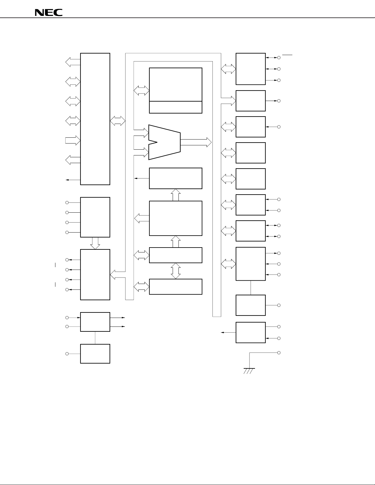
BLOCK DIAGRAM
µ
PD17072,17073
P0A0-P0A3
P0B0-P0B3
P0C0, P0C1
P0D2, P0D3
P1A0-P1A3
P1B0-P1B3
P1C0
LCD
REG
LCD
REG
CAP
LCD
LCD
CAP
SCK/P0B2
Serial
Interface
RAM
SI/SO1/P0B3
SO0/P1C0
176×4 bits
BEEP
BEEP
SYSTEM REG.
Port
Interrupt
Controller
INT
ALU
Basic Timer0
Instruction
Decoder
0
1
0
Voltage
Doubler
3072×16 bits ( PD17072)
4096×16 bits ( PD17073)
ROM
µ
µ
1
Basic Timer1
A/D
Converter
Frequency
Counter
AD0/P1A2
AD1/P1A3
FMIFC/AMIFC/P0D3
AMIFC/P0D2
COM0
COM3
LCD0
LCD14
X
X
OUT
REG1
LCD
Controller
/Driver
Program Counter
12 bits
PLL
Stack
EO
VCOH
VCOL
2×12 bits
PLL
Voltage
REG0
Regulator
IN
OSC
XTAL
Voltage
CPU
Peripheral
Reset
DD
V
CE
GND
Regulator
4
Page 5
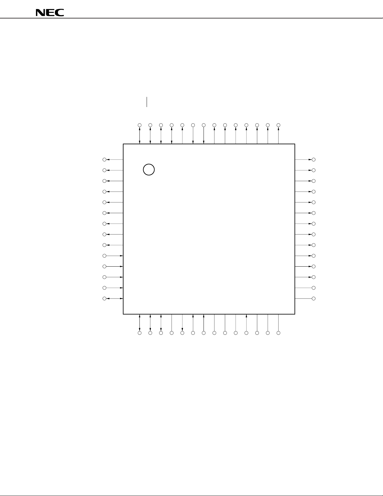
PIN CONFIGURATION (Top View)
1
2
3
4
5
6
7
8
9
10
11
12
13
14
42
41
40
39
38
37
36
35
34
33
32
31
30
29
15 16 17 18 19 20 21 22 23 24 25 26 27 28
56 55 54 53 52 51 50 49 48 47 46 45 44 43
P1C0/SO0
P0A0
P0A1
P0A2
P0A3
P1B0
P1B1
P1B2
P1B3
P1A0
P1A1
P1A2/AD0
P1A3/AD1
P0C0
LCD7
LCD6
LCD5
LCD4
LCD3
LCD2
LCD1
LCD0
COM3
COM2
COM1
COM0
REG
LCD1
CAP
LCD1
P0B3/SI/SO1
P0B2/SCK
P0B1
P0B0
BEEP
INT
CE
LCD14
LCD13
LCD12
LCD11
LCD10
LCD9
LCD8
P0C1
P0D2/AMIFC
P0D3/FMIFC/AMIFC
GND
EO
VCOL
VCOH
REG0
V
DD
XOUT
XIN
REG1
REG
LCD0
CAP
LCD0
56-pin plastic QFP (10 × 10 mm)
µ
PD17072GB-×××-1A7
µ
PD17073GB-×××-1A7
µ
PD17072,17073
5
Page 6
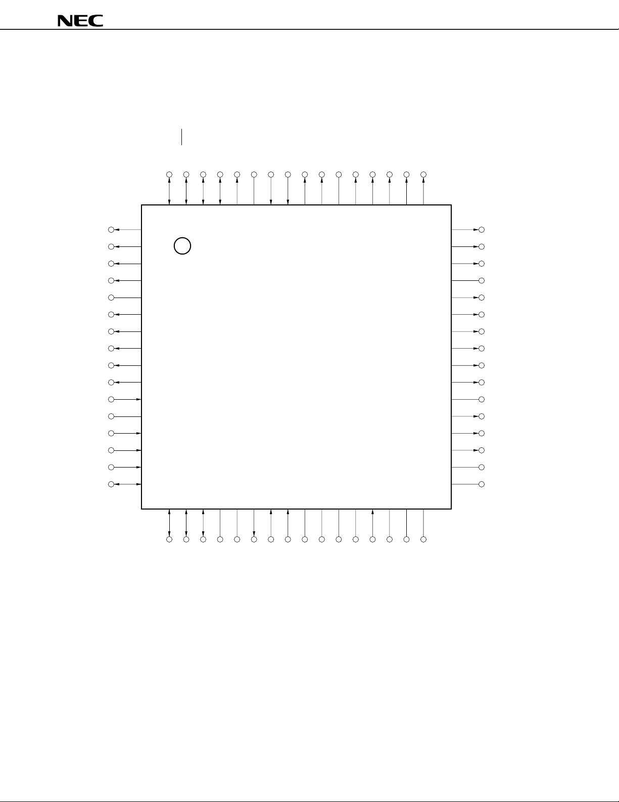
64-pin plastic TQFP (fine pitch) (10 × 10 mm)
µ
PD17072GB-×××-9EU
µ
PD17073GB-×××-9EU
P0B3/SI/SO1
P0B2/SCK
P0B1
P0B0
BEEPNCINT
64 63 62 61 60 59 58 57 56 55 54 53 52 51 50 49
P1C0/SO0
P0A0
P0A1
P0A2
NC
P0A3
P1B0
P1B1
P1B2
P1B3
P1A0
NC
P1A1
P1A2/AD0
P1A3/AD1
P0C0
1
2
3
4
5
6
7
8
9
10
11
12
13
14
15
16
CE
LCD14
LCD13NCLCD12
LCD11
LCD10
LCD9
µ
PD17072,17073
LCD8
48
47
46
45
44
43
42
41
40
39
38
37
36
35
34
33
LCD7
LCD6
LCD5
NC
LCD4
LCD3
LCD2
LCD1
LCD0
COM3
NC
COM2
COM1
COM0
REG
CAP
LCD
LCD
1
1
17 18 19 20 21 22 23 24 25 26 27 28 29 30 31 32
0
P0C1
GND
GND
EO
VCOL
VCOH
REG0
DDVDD
V
OUT
X
IN
X
REG1
LCD
REG
0
LCD
CAP
P0D2/AMIFC
P0D3/FMIFC/AMIFC
6
Page 7

PIN IDENTIFICATION
AD0, AD1 : A/D converter input
AMIFC : Intermediate frequency (IF) counter input
BEEP : BEEP output
CLD0, CAPLCD1 : Capacitor connection for LCD drive voltage
CAP
CE : Chip enable
COM0-COM2 : LCD common signal output
EO : Error out
FMIFC : Intermediate frequency (IF) counter input
GND : Ground
INT : External interrupt request signal input
LCD0-LCD14 : LCD segment signal output
NC : No connection
P0A0-P0A3 : Port 0A
P0B0-P0B3 : Port 0B
P0C0, P0C1 : Port 0C
P0D2, P0D3 : Port 0D
P1A0-P1A3 : Port 1A
P1B0-P1B3 : Port 1B
P1C0 : Port 1C
LCD0, REGLCD1 : LCD drive voltage
REG
REG0 : PLL voltage regulator
REG1 : Oscillation circuit voltage regulator
SCK : Serial clock I/O
SI : Serial data input
SO0, SO1 : Serial data output
VCOL : Local oscillator input
VCOH : Local oscillator input
DD : Positive power supply
V
XIN, XOUT : Crystal resonator connection pins
µ
PD17072,17073
7
Page 8

µ
PD17072,17073
CONTENTS
1. PIN FUNCTION.................................................................................................................................. 12
1.1 Pin Function List ...................................................................................................................................... 12
1.2 Equivalent Circuits of Pins....................................................................................................................... 15
1.3 Processing of Unused Pins ..................................................................................................................... 18
1.4 Notes on Using CE Pin............................................................................................................................ 19
2. PROGRAM MEMORY (ROM) ........................................................................................................... 20
2.1 General ..................................................................................................................................................... 2 0
2.2 Program Memory ..................................................................................................................................... 21
2.3 Program Counter......................................................................................................................................21
2.4 Execution Flow of Program Memory ....................................................................................................... 2 2
2.5 Notes on Using Program Memory........................................................................................................... 22
3. ADDRESS STACK (ASK) ................................................................................................................. 23
3.1 General ..................................................................................................................................................... 2 3
3.2 Address Stack Register (ASR) ................................................................................................................ 23
3.3 Stack Pointer (SP) ................................................................................................................................... 24
3.4 Operations of Address Stack................................................................................................................... 25
3.5 Notes on Using Address Stack................................................................................................................ 2 5
4. DATA MEMORY (RAM) ..................................................................................................................... 26
4.1 General ..................................................................................................................................................... 2 6
4.2 Configuration and Function of Data Memory.......................................................................................... 27
4.3 Addressing Data Memory ........................................................................................................................ 30
4.4 Notes on Using Data Memory ................................................................................................................. 31
5. SYSTEM REGISTER (SYSREG) ...................................................................................................... 32
5.1 General ..................................................................................................................................................... 3 2
5.2 Address Register (AR)............................................................................................................................. 33
5.3 Bank Register (BANK) ............................................................................................................................. 35
5.4 Program Status Word (PSWORD).......................................................................................................... 36
5.5 Notes on Using System Register ............................................................................................................ 37
6. GENERAL REGISTERS (GR)........................................................................................................... 38
6.1 Outline of General Registers ................................................................................................................... 38
6.2 Address Creation of General Register with Each Instruction ................................................................ 3 9
6.3 Notes on Using General Register ........................................................................................................... 39
7. ALU (ARITHMETIC LOGIC UNIT) BLOCK....................................................................................... 40
7.1 General ..................................................................................................................................................... 4 0
7.2 Configuration and Function of Each Block ............................................................................................. 41
7.3 ALU Processing Instructions ................................................................................................................... 41
7.4 Notes on Using ALU ................................................................................................................................44
8
Page 9

µ
PD17072,17073
8. PERIPHERAL CONTROL REGISTERS ........................................................................................... 45
8.1 Outline of Peripheral Control Registers .................................................................................................. 45
8.2 Configuration and Function of Peripheral Control Registers ................................................................. 46
9. DATA BUFFER (DBF) ....................................................................................................................... 54
9.1 General ..................................................................................................................................................... 5 4
9.2 Data Buffer ............................................................................................................................................... 55
9.3 List of Peripheral Hardware and Data Buffer Functions ........................................................................ 56
9.4 Notes on Using Data Buffer ..................................................................................................................... 56
10. GENERAL-PURPOSE PORT ............................................................................................................ 57
10.1 General..................................................................................................................................................... 57
10.2 General-Purpose I/O Ports (P0B, P0C, P0D) ......................................................................................... 58
10.3 General-Purpose Input Ports (P1A) ........................................................................................................ 62
10.4 General-Purpose Output Ports (P0A, P1B, P1C)................................................................................... 6 5
11. INTERRUPT....................................................................................................................................... 6 6
11.1 General..................................................................................................................................................... 66
11.2 Interrupt Control Block............................................................................................................................. 67
11.3 Interrupt Stack Register........................................................................................................................... 70
11.4 Stack Pointer, Address Stack Register, and Program Counter ............................................................. 72
11.5 Interrupt Enable Flip-Flop (INTE)............................................................................................................ 72
11.6 Accepting Interrupt................................................................................................................................... 73
11.7 Operations after Accepting Interrupt ....................................................................................................... 77
11.8 Exiting from Interrupt Service Routine.................................................................................................... 78
11.9 External (INT Pin) Interrupts ................................................................................................................... 79
11.10 Internal Interrupt....................................................................................................................................... 81
12. TIMER ................................................................................................................................................ 82
12.1 General..................................................................................................................................................... 82
12.2 Basic Timer 0 ........................................................................................................................................... 82
12.3 Basic Timer 1 ........................................................................................................................................... 91
13. A/D CONVERTER ............................................................................................................................. 98
13.1 General..................................................................................................................................................... 98
13.2 Setting A/D Converter Power Supply ...................................................................................................... 99
13.3 Input Selector Block............................................................................................................................... 100
13.4 Compare Voltage Generator Block and Compare Block ..................................................................... 102
13.5 Comparison Timing Chart...................................................................................................................... 107
13.6 Perfor mance of A/D Converter .............................................................................................................. 107
13.7 Using A/D Converter .............................................................................................................................. 108
13.8 Status at Reset .......................................................................................................................................111
14. SERIAL INTERFACE ....................................................................................................................... 112
14.1 General................................................................................................................................................... 112
14.2 Clock Input/Output Control Block and Data Input/Output Control Block............................................. 113
14.3 Clock Control Block ............................................................................................................................... 116
14.4 Clock Counter ........................................................................................................................................ 116
9
Page 10

µ
PD17072,17073
14.5 Presettable Shift Register...................................................................................................................... 117
14.6 Wait Control Block ................................................................................................................................ . 117
14.7 Serial Interface Operation ..................................................................................................................... 118
14.8 Notes on Setting and Reading Data ..................................................................................................... 122
14.9 Operational Outline of Serial Interface ................................................................................................. 123
14.10 Status on Reset ..................................................................................................................................... 125
15. PLL FREQUENCY SYNTHESIZER ................................................................................................ 126
15.1 General................................................................................................................................................... 126
15.2 Input Selector Block and Programmable Divider ................................................................................. 127
15.3 Reference Frequency Generator ........................................................................................................... 133
φ
15.4 Phase Comparator (
15.5 PLL Disable Status ................................................................................................................................ 139
15.6 Use of PLL Frequency Synthesizer ...................................................................................................... 1 40
15.7 Status on Reset ..................................................................................................................................... 143
-DET), Charge Pump, and Unlock FF ............................................................... 135
16. INTERMEDIATE FREQUENCY (IF) COUNTER ............................................................................. 14 4
16.1 Outline of Intermediate Frequency (IF) Counter .................................................................................. 1 44
16.2 IF Counter Input Selector Block and Gate Time Control Block ........................................................... 145
16.3 Start Control Block and IF Counter....................................................................................................... 147
16.4 Using IF Counter.................................................................................................................................... 152
16.5 Status at Reset ...................................................................................................................................... 154
17. BEEP................................................................................................................................................ 1 55
17.1 Configuration and Function of BEEP .................................................................................................... 155
17.2 Output Wave Form of BEEP ................................................................................................................. 156
17.3 Status at Reset ...................................................................................................................................... 157
18. LCD CONTROLLER/DRIVER ......................................................................................................... 15 8
18.1 Outline of LCD Controller/Driver ........................................................................................................... 158
18.2 LCD Drive Voltage Generation Block .................................................................................................... 159
18.3 LCD Segment Register.......................................................................................................................... 160
18.4 Common Signal Output and Segment Signal Output Timing Control Blocks ..................................... 162
18.5 Common Signal and Segment Signal Output Waves .......................................................................... 163
18.6 Using LCD Controller/Driver.................................................................................................................. 165
18.7 Status at Reset ...................................................................................................................................... 167
19. STANDBY ........................................................................................................................................ 168
19.1 General................................................................................................................................................... 168
19.2 Halt Function .......................................................................................................................................... 1 70
19.3 Clock Stop Function............................................................................................................................... 178
19.4 Device Operations in Halt and Clock Stop Statuses ............................................................................ 181
19.5 Note on Processing of Each Pin in Halt and Clock Stop Statuses ..................................................... 1 82
19.6 Device Control Function by CE Pin ...................................................................................................... 185
19.7 Low-Speed Mode Function .................................................................................................................... 187
10
Page 11

µ
PD17072,17073
20. RESET .............................................................................................................................................. 188
20.1 Configuration of Reset Block................................................................................................................. 1 88
20.2 Reset Function ....................................................................................................................................... 18 9
20.3 CE Reset ................................................................................................................................................ 190
20.4 Power-ON Reset .................................................................................................................................... 19 4
20.5 Relations between CE Reset and Power-ON Reset............................................................................ 197
20.6 Power Failure Detection ........................................................................................................................ 199
21.µPD17012 INSTRUCTIONS ............................................................................................................ 20 4
21.1 Instruction Set Outline ........................................................................................................................... 204
21.2 Legend.................................................................................................................................................... 20 5
21.3 Instruction List........................................................................................................................................ 206
21.4 Assembler (AS17K) Embedded Macroinstructions .............................................................................. 207
22.µPD17073 RESERVED WORDS .................................................................................................... 208
22.1 Data Buffer (DBF) .................................................................................................................................. 208
22.2 System Register (SYSREG).................................................................................................................. 208
22.3 LCD Segment Register.......................................................................................................................... 209
22.4 Port Register .......................................................................................................................................... 210
22.5 Peripheral Control Register ................................................................................................................... 211
22.6 Peripheral Hardware Register .....................................................................................................................
22.7 Others..................................................................................................................................................... 213
23. ELECTRICAL CHARACTERISTICS ............................................................................................... 214
24. PACKAGE DRAWINGS ................................................................................................................... 217
25. RECOMMENDED SOLDERING CONDITIONS .............................................................................. 219
APPENDIX A. NOTES ON CONNECTING CRYSTAL RESONATOR................................................220
APPENDIX B. DEVELOPMENT TOOLS ..............................................................................................221
11
Page 12
µ
PD17072,17073
1. PIN FUNCTION
1.1 Pin Function List
Pin No. Symbol Function Output format At power-ON
QFP TQFP reset
1 1 P1C0/SO0 Port 1C and output of serial interface. CMOS push-pull Low-level output
P1C0
•
• 1-bit output port
SO0
•
• Serial data output
2 2 P0A0 4-bit output port (port 0A). CMOS push-pull Low-level output
3 3 P0A1
4 4 P0A2
5 6 P0A3
6 7 P1B0 4-bit output port (port 1B). CMOS push-pull Low-level output
7 8 P1B1
8 9 P1B2
9 10 P1B3
10 11 P1A0 Port 1A and analog inputs to A/D converter. — Inputs with pull11 13 P1A1
12 14 P1A2/AD0 • 4-bit input port
13 15 P1A3/AD1
14 16 P0C0 2-bit I/O port (port 0C). CMOS push-pull Input
15 17 P0C1 Input/output mode can be set in 1-bit units.
16 18 P0D2/AMIFC Port 0D and IF counter inputs. CMOS push-pull Input
17 19 P0D3/FMIFC/•P0D3, P0D2
AMIFC • 2-bit I/O port
18 20 GND Ground — —
21
19 22 EO Output from charge pump of PLL frequency synthesizer CMOS 3-state Floating
20 23 VCOL Input local oscillation frequency of PLL. — Floating
21 24 VCOH
22 25 REG0 Output of PLL voltage regulator. — Low-level output
P1A3-P1A0 down resistor
•
AD1, AD0
•
• Analog inputs to A/D converter
• Can be set in input/output mode in 1-bit units.
FMIFC, AMIFC
•
• IF counter inputs
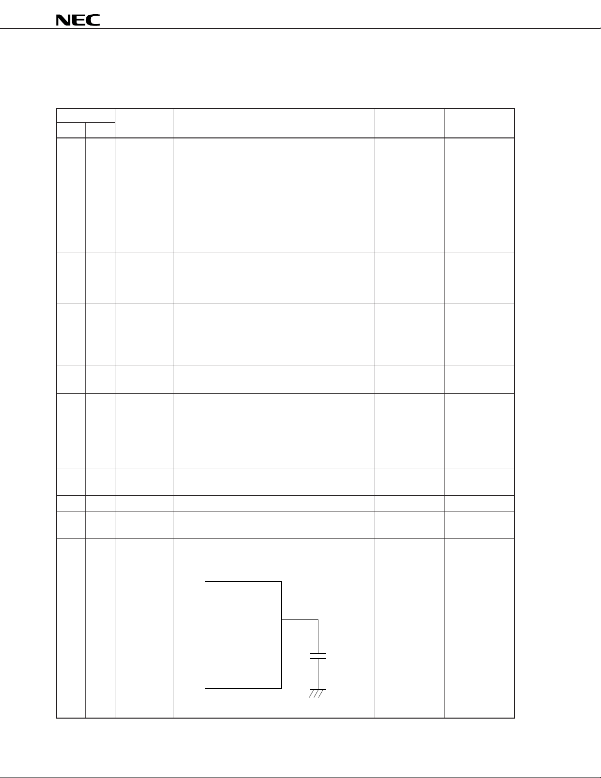
Connect this pin to GND via 0.1-µF capacitor.
12
REG0
0.1 F
µ
Page 13
µ
PD17072,17073
Pin No. Symbol Function Output format At power-ON
QFP TQFP reset
23 26 VDD Positive power supply. — —
27 Supply 1.8 to 3.6 V (TA = –20 to +70 °C) to operate
all functions.
Do not apply voltage higher than that of VDD pin to
any pin other than VDD.
24 28 XOUT Pins for connecting crystal resonator for system CMOS push-pull —
25 29 XIN
26 30 REG1 Output of voltage regulator for oscillation circuit. — —
clock oscillation.
Connect this pin to GND via 0.1-µF capacitor.
REG1
0.1 F
—
µ
27 31 REGLCD0
28 32 CAPLCD0 LCD drive power pins.
29 33 CAPLCD1
30 34 REGLCD1 Connect capacitors for doubler circuit to generate
REGLCD1, REGLCD0——
•
CAPLCD1, CAPLCD0
•
LCD drive voltage, across these pins.
To configure doubler circuit, connect capacitors
as shown below.
REG
CAP
CAP
REG
LCD
LCD
LCD
LCD
C1 = C2 = 0.1 F
C3 = 0.01 F
C1
1
1
C3
0
0
C2
µ
µ
Caution The value of the LCD drive voltage differs
if the values of C1, C2, and C3 are changed
because of the configuration of the doubler
circuit.
13
Page 14
µ
PD17072,17073
Pin No. Symbol Function Output format At power-ON
QFP TQFP reset
31 35 COM0 Common signal outputs of LCD controller/driver. CMOS ternary Low-level output
32 36 COM1 output
33 37 COM2
34 39 COM3
35 40 LCD0 Segment signal outputs of LCD controller/driver. CMOS push-pull Low-level output
| | |
49 56 LCD14
50 57 CE Device operation select and reset signal input. — Input
51 58 INT External interrupt request signal input. — Input
Interrupt request is issued at rising or falling edge
of signal input to this pin.
52 60 BEEP BEEP signal output pin. CMOS push-pull Low-level output
BEEP output of 1.5 kHz or 3 kHz can be selected.
53 61 P0B0 Port 0B and serial interface I/O. CMOS push-pull Input
54 62 P0B1
55 63 P0B2/SCK • 4-bit I/O port
56 64 P0B3/SI/SO1 • Can be set in input or output mode in 1-bit units.
— 5 NC No connection — —
12
38
45
54
59
P0B3-P0B0
•
SCK
•
• Serial clock I/O
SO1
•
• Serial data output
SI
•
• Serial data input
14
Page 15
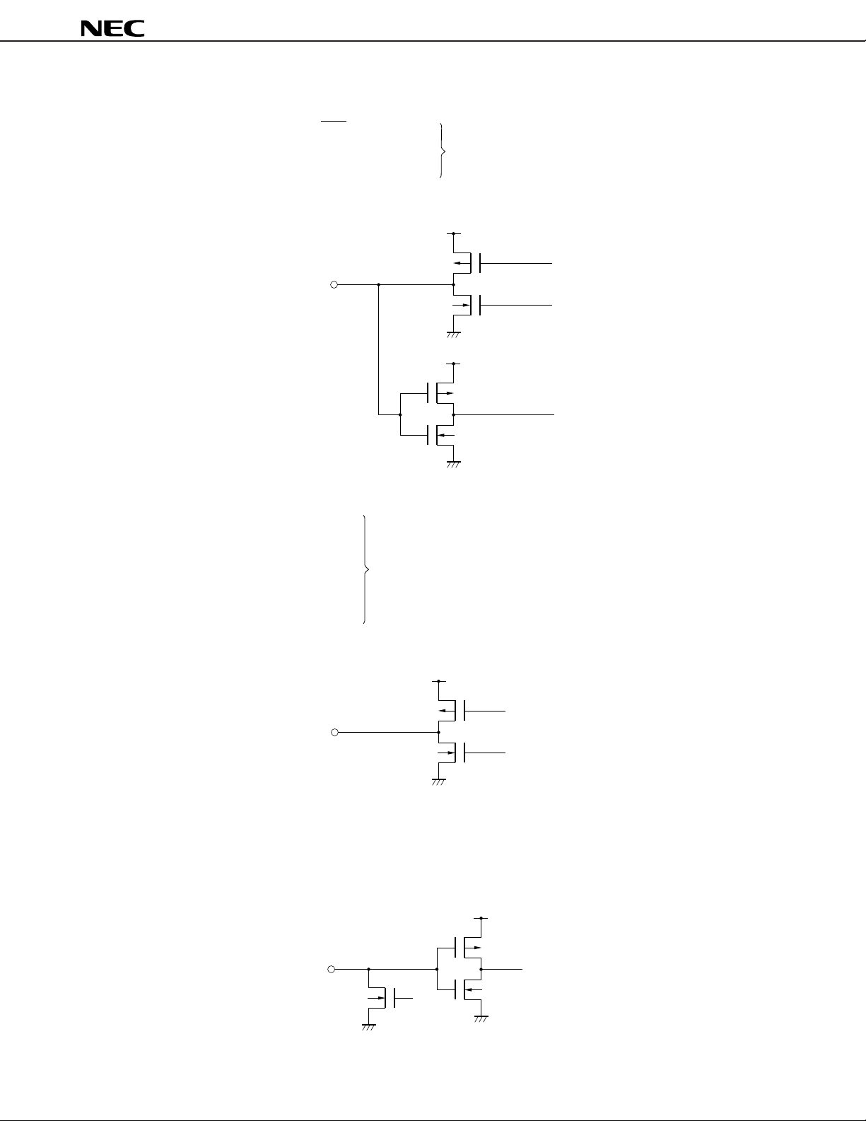
1.2 Equivalent Circuits of Pins
(1) P0B (P0B3/SI/SO1, P0B2/SCK, P0B1, P0B0)
P0C (P0C1, P0C0) (I/O)
P0D (P0D3/FMIFC/AMIFC, P0D2/AMIFC)
µ
PD17072,17073
V
DD
V
DD
(2) P0A (P0A3, P0A2, P0A1, P0A0)
P1B (P1B3, P1B2, P1B1, P1B0)
P1C (P1C0/SO0)
LCD14-LCD0
(Output)
BEEP
EO
V
DD
(3) P1A (P1A3/AD1, P1A2/AD0, P1A1, P1A0) (Input)
V
DD
High ON
resistance
15
Page 16
(4) CE (Schmitt trigger input)
(5) INT (Schmitt trigger input)
µ
PD17072,17073
V
DD
CE flag
(6) XOUT (output), XIN (input)
X
IN
V
DD
V
DD
High ON
resistance
V
DD
16
High ON
resistance
OUT
X
Page 17
(7) COM3 through COM0 (output)
(8) VCOH (input)
µ
PD17072,17073
V
V
LCD0
LCD1
High ON resistance
(9) VCOL (input)
VDD
PLL disable signal
VDD
High ON resistance
VDD
PLL disable signal
High ON resistance
VDD
17
Page 18
1.3 Processing of Unused Pins
It is recommended that the unused pins be connected as follows:
Table 1-1. Processing of Unused Pins
Pin name I/O mode Recommended processing of unused pins
Port pin P0A0-P0A3 CMOS push-pull output Open
P0B0, P0B1 I/O
P0B2/SCK
P0B3/SI/SO1
P0C0, P0C1
P0D2/AMIFC
P0D3/FMIFC/AMIFC
P1A0, P1A1 Input Connect each of these pins to VDD or GND via resistor
P1A2/AD0
P1A3/AD1
P1B0-P1B3 CMOS push-pull output Open
P1C0/SO0
Pins other BEEP CMOS push-pull output Open
than port
pins
CE Input Connect to VDD via resistor
COM0-COM3 Output Open
EO Output
INT Input Connect to GND via resistor
LCD0-LCD14 CMOS push-pull output Open
VCOH, VCOL Input Connect each of these pins to GND via resistor
Note 1
Set by software to output low level and open
Note 2
Note 2
µ
PD17072,17073
Note 2
.
.
.
Note 2
.
Notes 1. The I/O ports are set in the input mode on power application, on clock stop, and on CE reset.
2. When pulling up (connecting to VDD via resistor) or pulling down (connecting to GND via resistor) a pin
externally with high resistance, the pin almost goes into a high-impedance state, and consequently, the
current consumption (through current) of the port increases. Generally, the pull-up or pull-down
resistance is several 10 kΩ, though it varies depending on the application circuit.
18
Page 19
µ
PD17072,17073
1.4 Notes on Using CE Pin
The CE pin has a function to set a test mode in which the internal operations of the µPD17073 are tested (dedicated
to IC test), in addition to the functions listed in 1.1 Pin Function List.
When a voltage higher than V
VDD is applied to the CE pin even during normal operation, the test mode is set, affecting the normal operation.
If the wiring of the CE pin is too long, the above problem occurs because wiring noise is superimposed on the CE
pin.
Therefore, wire the CE pin with as short a wiring length as possible to suppress noise. If noise cannot be avoided,
use external components as shown below to suppress noise.
DD is applied to the CE pin, the test mode is set. This means that if noise exceeding
• Connect a diode with low V
Diode with
F
low V
CE
F between CE and VDD • Connect a capacitor between CE and VDD
V
DD
V
DD
CE
V
DD
V
DD
19
Page 20
µ
2. PROGRAM MEMORY (ROM)
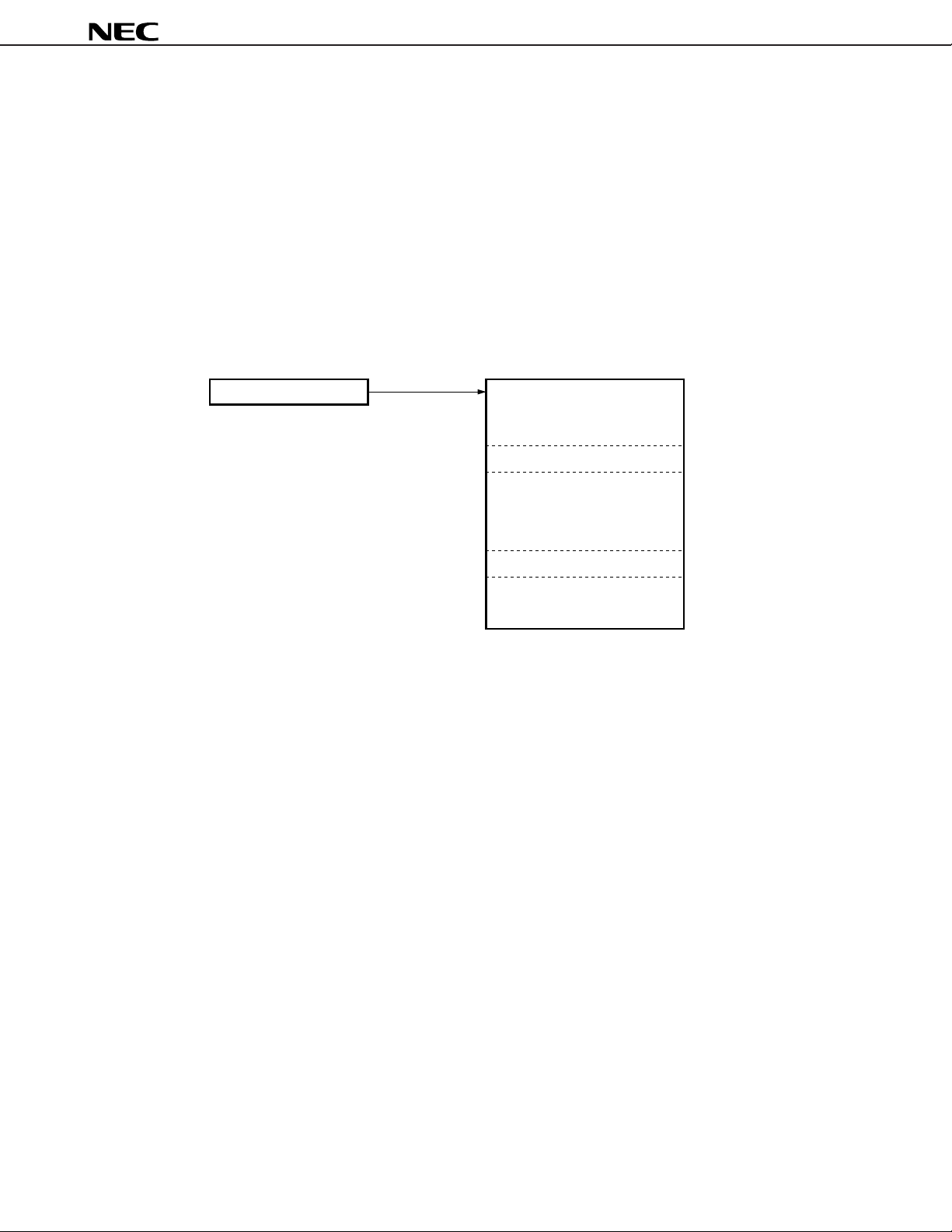
2.1 General
Figure 2-1 shows the configuration of the program memory.
As shown in this figure, the program memory consists of a program memory and a program counter.
The addresses of the program memory are specified by the program counter.
The program memory has the following two major functions:
(1) Stores program
(2) Stores constant data
Figure 2-1. Outline of Program Memory
PD17072,17073
Program counter
Specifies address
Program memory
•
•
•
Instruction
•
•
•
•
•
•
Constant data
•
•
•
20
Page 21
µ
PD17072,17073
2.2 Program Memory
Figure 2-2 shows the configuration of the program memory.
As shown in this figure, the program memory is configured as follows:
µ
PD17072: 3072 × 16 bits (0000H-0BFFH)
µ
PD17073: 4096 × 16 bits (0000H-0FFFH)
Therefore, the addresses of the program memory range from 0000H to 0FFFH.
All the “instructions” are “one-word instructions” each of which is 16 bits long. Consequently, one instruction can
be stored in one address of the program memory.
As constant data, the contents of the program memory are read to the data buffer by using a table reference
instruction.
Figure 2-2. Configuration of Program Memory
0
0
0
0
H
0
0
0
1
H
0
0
0
2
H
0
0
0
3
H
Reset start address
Serial interface interrupt vector
Basic timer 1 interrupt vector
INT pin interrupt vector
Page 0
CALL addr
instruction
subroutine
entry address
BR addr
instruction
branch address
BR @AR
instruction
branch address
CALL @AR
0
7
F
F
H
0
B
F
F
H
0
F
F
F
H
Caution With the
µ
(with PD17072)
(with PD17073)
µ
16 bits
µ
PD17072, the range of addresses that can be called by each instruction is 0000H to
Page 1
instruction
subroutine entry
address
MOVT DBF @AR
instruction table
reference address
0BFFH. The area from addresses 0C00H through 0FFFH is an undefined area.
2.3 Program Counter
Figure 2-3 shows the configuration of the program counter.
The program counter specifies an address of the program memory.
As shown in this figure, the program counter is a 12-bit binary counter. The most significant bit b
page.
11 indicates a
PC
11
Page
PC
Figure 2-3. Configuration of Program Counter
10
PC
9
PC
8
PC
7
PC
PC
PC
6
5
PC
4
PC
3
PC
2
PC
1
PC
0
21
Page 22
µ
PD17072,17073
2.4 Execution Flow of Program Memory
Execution of the program is controlled by the program counter which specifies an address of the program memory.
Figure 2-4 shows the values to be set to the program counter when each instruction is executed.
Table 2-1 shows the vector addresses that are to be set to the program counter when each interrupt occurs.
Figure 2-4. Specification by Program Counter On Execution of Each Instruction
Instruction
BR addr
CALL addr
BR @AR
CALL @AR
MOVT DBF, @AR
RET
RETSK
RETI
When interrupt is accepted
Power-ON reset, CE reset
Priority Internal/external Interrupt source Vector address
Program counter
Page 0
Page 1
11 b10 b9 b8 b7 b6 b5 b4 b3 b2 b1 b0
b
0
1
0
000000000000
Contents of program counter (PC)
Instruction operand (addr)
Instruction operand (addr)
Contents of address register
Contents of address stack register (ASR)
specified by stack pointer (SP)
(Return address)
Vector address of each interrupt
Table 2-1. Interrupt Vector Address
1 External INT pin 0003H
2 External Basic timer 1 0002H
3 External Serial interface 0001H
2.5 Notes on Using Program Memory
(1)µPD17072
The program memory addresses of the µPD17072 are 0000H through 0BFFH. However, because the
addresses that can be specified by the program counter (PC) are 0000H through 0FFFH, keep the following
points in mind when specifying a program memory address:
• Be sure to write a branch instruction to address 0BFFH, when writing an instruction to this address.
• Do not write an instruction to addresses 0C00H through 0FFFH.
• Do not branch to addresses 0C00H through 0FFFH.
µ
(2) With
PD17073
The program memory addresses of the µPD17073 are 0000H through 0FFFH. Keep the following point in mind:
• Be sure to write a branch instruction to address 0FFFH, when writing an instruction to this address.
22
Page 23
µ
PD17072,17073
3. ADDRESS STACK (ASK)
3.1 General
Figure 3-1 outlines the address stack.
The address stack consists of a stack pointer and an address stack register.
The address of the address stack register is specified by the stack pointer.
The address stack saves return addresses when a subroutine call instruction has been executed and when an
interrupt has been accepted.
The address stack is also used when a table reference instruction is executed.
Figure 3-1. Outline of Address Stack
Stack pointer Address stack register
Specifies address
Return address
3.2 Address Stack Register (ASR)
Figure 3-2 shows the configuration of the address stack register.
The address stack register consists of three 12-bit registers ASR0-ASR2. Actually, however, no register is
assigned to ASR2, and the address stack register therefore consists of two 12-bit registers (ASR0 and ASR1).
The address stack saves return addresses when a subroutine call instruction has been executed, when an interrupt
has been accepted, and when a table reference instruction is executed.
Figure 3-2. Configuration of Address Stack Register
Stack pointer
(SP)
Bit
3b2b1b0
b
0 0 SP1 SP0
Address
0H
1H
2H
b
11b10b9b8b7b6b5b4b3b2b1b0
Address stack register (ASR)
Bit
ASR0
ASR1
ASR2 (Undefined)
Cannot
be used
23
Page 24
µ
PD17072,17073
3.3 Stack Pointer (SP)
Figure 3-3 shows the configuration and functions of the stack pointer.
The stack pointer is a 4-bit binary counter.
The stack pointer specifies the addresses of the address stack registers.
The value of the stack pointer can be directly read or written by using a register manipulation instruction.
Figure 3-3. Configuration and Functions of Stack Pointer
At
reset
Name
Stack pointer
SP
Power-ON
Clock stop
CE
Flag symbol
3b2b1b0
b
S
0
0
0010
S
P
P
1
0
00
01
10
10
10
Address
01H R/W
Address 0 (ASR0)
Address 1 (ASR1)
Address 2 (ASR2)
Fixed to "0"
Read/
Write
Specifies address of address stack register (ASR)
24
Page 25

µ
PD17072,17073
3.4 Operations of Address Stack
3.4.1 Subroutine call (“CALL addr” or “CALL @AR”) and return (“RET” or “RETSK”) instructions
When a subroutine call instruction is executed, the value of the stack pointer is decremented by one and the return
address is stored to the address stack register specified by the stack pointer.
When a return instruction is executed, the contents of the address stack specified by the stack pointer (return
address) is restored to the program counter, and the value of the stack pointer is incremented by one.
3.4.2 Table reference instruction (“MOVT DBF, @AR”)
When the table reference instruction is executed, the value of the stack pointer is decremented by one and the
return address is stored to the address stack register specified by the stack pointer.
Next, the contents of the program memory addressed by the address register are read to the data buffer, and the
contents of the address stack register specified by the stack pointer (return address) are restored to the program
counter. The value of the stack pointer is then incremented by one.
3.4.3 On acceptance of interrupt and execution of return instruction (“RETI” instruction)
When an interrupt is accepted, the value of the stack pointer is decremented by one, and the return address is
stored to the address stack register specified by the stack address.
When the return instruction is executed, the contents of the address stack register specified by the stack pointer
(return address) are restored to the program counter and the value of the stack pointer is incremented by one.
3.4.4 Address stack manipulation instructions (“PUSH AR” and “POP AR”)
When the “PUSH” instruction is executed, the value of the stack pointer is decremented by one, and the contents
of the address register are transferred to the address stack register specified by the stack pointer.
When the “POP” instruction is executed, the contents of the address stack register specified by the stack pointer
are transferred to the address register, and the value of the stack pointer is incremented by one.
3.5 Notes on Using Address Stack
The nesting level of the address stack is two, and the value of the address stack register ASR2 is “undefined” when
the value of the stack pointer is 2H.
Consequently, if a subroutine is called or an interrupt is used exceeding 2 levels without manipulating the stack,
program execution returns to an “undefined” address.
25
Page 26
µ
PD17072,17073
4. DATA MEMORY (RAM)
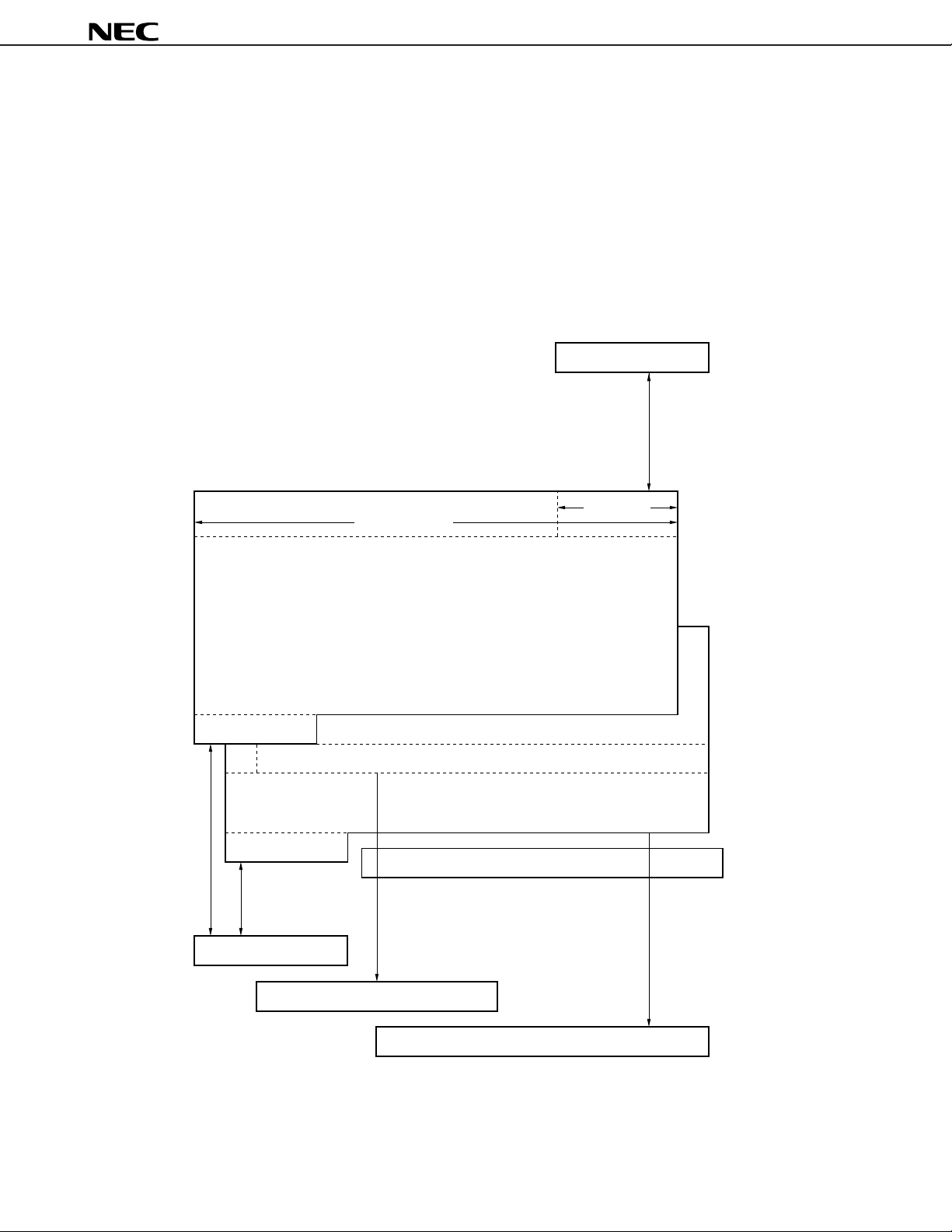
4.1 General
Figure 4-1 outlines the data memory.
As shown in this figure, the data memory consists of a general-purpose data memory, system register, data buffer,
general register, LCD segment register, port register, and peripheral control register.
The data memory stores data, transfers data with peripheral hardware, sets conditions for the peripheral hardware,
display data, transfers data with ports, and controls the CPU.
Figure 4-1. Outline of Data Memory
Peripheral hardware
Data transfer
Column address
0123456789ABCDEF
0
1
2
3
4
Row address
5
6
Port register BANK1
7
Port register
Data transfer
Port
Data buffer
General register
Data memory
BANK0
LCD segment register
Peripheral control register
System register
Data transfer
26
LCD
Condition
setting
Peripheral hardware
Page 27

µ
PD17072,17073
4.2 Configuration and Function of Data Memory
Figure 4-2 shows the configuration of the data memory.
As shown in this figure, the data memory is divided into three banks, and each bank consists of 128 nibbles with
7H row addresses and 0FH column addresses.
In terms of function, the data memory can be divided into six blocks each of which is described in the following
paragraphs 4.2.1 through 4.2.8.
The contents of the data memory can be operated, compared, judged, and transferred in 4-bit units by data memory
manipulation instructions.
Table 4-1 lists the data memory manipulation instructions.
4.2.1 System registers (SYSREG)
The system registers are allocated to addresses 74H through 7FH.
These registers are allocated independently of the bank and directly control the CPU. The same system registers
exist at addresses 74H through 7FH of each bank.
µ
With the
and PSWORD (program status word: addresses 7EH and 7FH) can be manipulated.
For details, refer to 5. SYSTEM REGISTER (SYSREG).
PD17073, only AR (address register: addresses 75H through 77H), BANK (bank register: address 79H),
4.2.2 Data buffer (DBF)
The data buffer is allocated to addresses 0CH through 0FH of BANK0.
The data buffer reads the constant data in the program memory (table reference), and transfers data with peripheral
hardware.
For details, refer to 9. DATA BUFFER (DBF).
4.2.3 General registers
µ
With the
and cannot be moved.
Operations and data transfer between the general registers and data memory can be executed with a single
instruction.
The general registers can be controlled by data memory manipulation instructions, like the other data memory
areas.
For details, refer to 6. GENERAL REGISTER (GR).
4.2.4 LCD segment registers
The LCD segment registers are allocated to addresses 41H through 4FH of BANK1 of the data memory, and are
used to set the display data of the LCD controller/driver.
For details, refer to 18. LCD CONTROLLER/DRIVER.
4.2.5 Port registers
The port registers are allocated to addresses 70H through 73H of BANK0 and addresses 70H through 73H of
BANK1, and are used to set the output data of each general-purpose port and read the data of the input ports.
For details, refer to 10. GENERAL-PURPOSE PORT.
PD17073, the general registers are fixed at row address 0 of BANK0, i.e., addresses 00H through 0FH,
4.2.6 Peripheral control registers
The peripheral control registers are allocated to addresses 50H through 6FH of BANK1 and are used to set the
conditions of the peripheral hardware (such as PLL, serial interface, A/D converter, IF counter, and timer).
For details, refer to 8. PERIPHERAL CONTROL REGISTER.
27
Page 28

µ
PD17072,17073
4.2.7 General-purpose data memory
The general-purpose data memory is allocated to the area of the data memory excluding the system register, LCD
segment register, port register, and peripheral control register.
µ
With the
be used as the general-purpose data memory.
4.2.8 Data memory areas not provided
For these data memory areas, refer to 4.4.2 Notes on data memory areas not provided, 8.2 Configuration and
Function of Peripheral Control Registers, and Table 10-1 Relation between Each Port (Pin) and Port Register.
PD17073, a total of 176 nibbles (176 × 4 bits), 112 nibbles of BANK0 and 64 nibbles of BANK1, can
28
Page 29
Figure 4-2. Configuration of Data Memory
Column address
0123456789ABCDEF
0
1
2
3
4
Row address
5
6
7
0
1
2
3
4
5
Row addressRow address
6
7
Data memory
BANK0
BANK1
System register
Column address
0123456789ABCDEF
General register
BANK0
Port register
System register (SYSREG)
Data buffer
µ
PD17072,17073
Example
Address 2BH
of BANK0
b
3b2b1b0
0123456789ABCDEF
0
1
2
3
4
5
6
Port register
7
BANK1
LCD segment register
Peripheral control register
System register (SYSREG)
Same system
register exists.
Caution Address 40H of BANK1, bit 3 of address 50H, and address 73H are test mode areas. Do not write
“1” to these areas.
29
Page 30
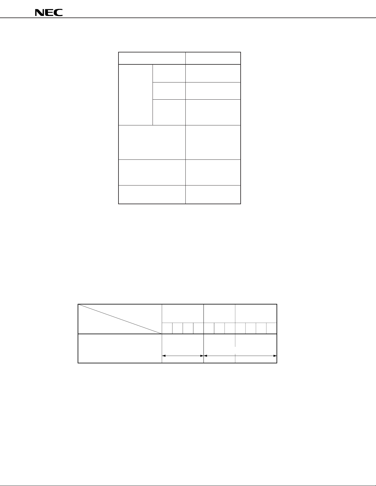
Table 4-1. Data Memory Manipulation Instructions
Function Instruction
µ
PD17072,17073
Add
Operation Subtract
Logical OR
Compare
Transfer LD
Judge
ADD
ADDC
SUB
SUBC
AND
XOR
SKE
SKGE
SKLT
SKNE
MOV
ST
SKT
SKF
4.3 Addressing Data Memory
Figure 4-3 shows how to address the data memory.
An address of the data memory is specified by using a bank, row address, and column address.
The row address and column address are directly specified by a data memory manipulation instruction, but the
bank is specified by the contents of the bank register.
For details of the bank register, refer to 5. SYSTEM REGISTER (SYSREG).
Figure 4-3. Addressing Data Memory
Data memory address M
Bank Row address Column address
b
b3b2b1b
Bank register Instruction operand
0
b2b
0
1
b3b2b1b
0
30
Page 31

µ
PD17072,17073
4.4 Notes on Using Data Memory
4.4.1 On power-ON reset
On power-ON reset, the contents of the general-purpose data memory are “undefined”.
Initialize the memory if necessary.
4.4.2 Notes on data memory not provided
If a data memory manipulation instruction is executed to manipulate an address where no data memory is assigned,
the following operations are performed:
(1) Device operation
When a read instruction is executed, “0” is read.
Nothing is changed even when a write instruction is executed.
Address 40H of BANK1, bit 3 of address 50H, and address 73H are test mode areas. Do not write “1” to these
areas.
(2) Assembler operation
The program is assembled normally. No “error” occurs.
(3) In-circuit emulator operation
“0” is read when a read instruction is executed.
Nothing is changed when a write instruction is executed.
No “error” occurs.
31
Page 32

µ
PD17072,17073
5. SYSTEM REGISTER (SYSREG)
5.1 General
Figure 5-1 shows the location of the system register on the data memory and outline.
As shown, the system register is assigned to addresses 74H-7FH of the data memory, regardless of bank. In other
words, the same system register is assigned to addresses 74H-7FH of any bank.
Since the system register is located on the data memory, it can be manipulated by all the data memory manipulation
instructions.
µ
With the
status word (PSWORD: 7EH, 7FH) of addresses 74H through 7FH can be manipulated.
PD17073, only the address register (AR: 74H through 77H), bank register (BANK: 79H), and program
Figure 5-1. Location of System Register on Data Memory and Outline
Column address
00123456789ABCDEF
1
2
3
4
5
Row address
6
7
Data memory
BANK0
BANK1
System register
Address 74H 75H 76H 77H 78H 79H
Name
Outline
Address 7AH 7BH 7CH 7DH 7EH 7FH
Name
Address register
(AR)
Controls program memory address
Fixed to 0
Fixed to 0 Bank register
(BANK)
Specifies data
memory bank
Program status word
(PSWORD)
32
Outline
Controls operation
Page 33

µ
PD17072,17073
5.2 Address Register (AR)
5.2.1 Configuration of address register
Figure 5-2 shows the configuration of the address register.
As shown in this figure, the address register consists of 16 bits of the system register: 74H through 77H (AR3
through AR0). However, the higher 4 bits are always fixed to 0, and therefore, the address register actually functions
as a 12-bit register.
Figure 5-2. Address Register Configuration
Address 74H 75H 76H 77H
Name
Symbol
Bit
AR3
3
2b1b0b3b2b1b0b3b2b1b0b3b2b1b0
b
b
Address register (AR)
AR2 AR1 AR0
M
Power-ON
Clock stop
At reset
CE
Data
000
0
0
0
0
Remark Power-ON : On power-ON reset
Clock stop : On execution of clock stop instruction
CE : On CE reset
L
S
B
0
0
0
0
0
0
S
B
0
0
0
33
Page 34

µ
PD17072,17073
5.2.2 Functions of address register
The address register specifies a program memory address when the table reference instruction (“MOVT DBF,
@AR”), stack manipulation instruction (“PUSH AR” or “POP AR”), indirect branch instruction (“BR @AR”), and indirect
subroutine call instruction (“CALL @AR”) has been executed.
A dedicated instruction (“INC AR”) that can increment the value of the address register by one is available.
The following paragraphs (1) through (5) describe the operations of the address register when each of these
instructions has been executed.
(1) Table reference instruction (“MOVT DBF, @AR”)
When the “MOVT DBF, @AR” instruction is executed, the constant data (16 bits) of the program memory
address specified by the contents of the address register are read to the data buffer.
The addresses of the constant data which can be specified by the address register are 0000H-0FFFH.
(2) Stack manipulation instruction (“PUSH AR”, “POP AR”)
By executing the “PUSH AR” instruction, the stack pointer is decremented by one and the contents of the
address register (AR) are stored to the address stack register specified by the stack pointer.
When the “POP AR” instruction is executed, the contents of the address stack register specified by the stack
pointer are transferred to the address register, and the stack pointer is incremented by one.
(3) Indirect branch instruction (“BR @AR”)
When the “BR @AR” instruction is executed, the program execution branches to a program memory address
specified by the contents of the address register.
The branch addresses that can be specified by the address register are 0000H-0FFFH.
(4) Indirect subroutine call instruction (“CALL @AR”)
When the “CALL @AR” instruction is executed, the subroutine at the program memory address specified by
the contents of the address register can be called.
The first addresses of the subroutine that can be specified by the address register are 0000H-0FFFH.
(5) Address register increment instruction (“INC AR”)
This instruction increments the contents of the address register by one each time it is executed.
Since the address register is configured of 12 bits, its contents become “0000H” when the “INC AR” instruction
is executed with the contents of the address register being “0FFFH”.
5.2.3 Address register and data buffer
The address register can transfer data through the data buffer as a part of the peripheral hardware.
For details, refer to 9. DATA BUFFER (DBF).
34
Page 35

µ
PD17072,17073
5.3 Bank Register (BANK)
5.3.1 Configuration of bank register
Figure 5-3 shows the configuration of the bank register.
As shown in this figure, the bank register consists of 4 bits of address 79H (BANK) of the system register. Note,
however, that the higher 3 bits are always fixed to “0”; therefore, this register actually serves as a 1-bit register.
Figure 5-3. Bank Register Configuration
Address 79H
Bank register
3
b
(BANK)
BANK
b
2
00
0
0
0
b1b
0
0
Power-ON
Clock stop
At reset
CE
Name
Symbol
Bit
Data
5.3.2 Function of bank register
The bank register selects a bank of the data memory.
Table 5-1 shows the value of the bank register and how a bank of the data memory is specified.
Since the bank register exists on the system register, its contents can be rewritten regardless of the currently
specified bank.
In other words, the current bank status has nothing to do with manipulation of the bank register.
Table 5-1. Specifying Bank of Data Memory
Bank register
(BANK)
b3 b2 b1 b0
––––––
0000
0001
––––––
––––––
Bank of data
memory
BANK0
BANK1
35
Page 36

µ
PD17072,17073
5.4 Program Status Word (PSWORD)
5.4.1 Configuration of program status word
Figure 5-4 shows the configuration of the program status word.
As shown in this figure, the program status word consists of a total of 5 bits: the least significant bit of address
7EH (RPL) and 4 bits of 7FH (PSW) of the system register. However, bit 0 of 7FH is always fixed to 0.
Each of the 5 bits in the program status word has its own function as a BCD flag (BCD), compare flag (CMP), carry
flag (CY), zero flag (Z), respectively.
Figure 5-4. Program Status Word Configuration
Power-ON
Clock stop
At reset
CE
Address
Name
Symbol
Bit
Data
7EH 7FH
Program status
0
0
0
word (PSWORD)
C
B
C
D
C
M
Y
P
0
0
0
Z
(RP)
RPL PSW
0 b2 b2 b0 b0 b2 b2 b0
b
0
36
Page 37

µ
PD17072,17073
5.4.2 Functions of program status word
The program status word sets conditions, under which the ALU (Arithmetic Logic Unit) performs arithmetic or
transfer operations, and indicates the results of the operations.
Table 5-2 outlines the function of each flag of the program status word.
For details, refer to 7. ALU (Arithmetic Logic Unit) BLOCK.
Table 5-2. Functional Outline of Each Flag of Program Status Word
(RP)
RPL PSW
3b2b1b0b3b2b1b0
b
Program status
word (PSWORD)
B
C
CYZ0
C
M
D
P
Flag name Function
Zero flag (Z)
Carry flag (CY)
Compare flag (CMP)
Indicates that the result of arithmetic operation is 0. Condition under which this flag is set differs depending on
contents of compare flag.
Indicates occurrence of carry or borrow as a result of
executing addition or subtraction instruction.
Reset (0) when carry or borrow does not occur. Set (1) when
carry or borrow occurs. Also used as shift bit of "RORC r"
instruction.
Stores or does not store result of arithmetic operation in
data memory or general register.
0: Stores result
1: Does not store result
BCD flag (BCD)
Executes arithmetic operation in decimal.
0: Executes binary operation
1: Executes decimal operation
5.4.3 Notes on using program status word
When an arithmetic operation (addition or subtraction) instruction is executed to the program status word, the result
of the arithmetic operation is stored in the program status word.
Even if an operation that generates a carry has been executed, for example, if the result of the operation is 0000B,
0000B is stored in PSW.
5.5 Notes on Using System Register
The data in the system register which are fixed to “0” are not influenced even when a write instruction is executed.
When these data are read, “0” is always read.
37
Page 38

µ
PD17072,17073
6. GENERAL REGISTERS (GR)
6.1 Outline of General Registers
With the µPD17073, the general registers are fixed at row address 0 of BANK0 on the data memory, and consist
of 16 nibbles (16 × 4 bits) of 00H through 0FH.
The 16 nibbles of the row address 0 specified as the general registers can perform operations and data transfer
with the data memory with a single instruction.
In other words, operations and data transfer between data memory areas can be executed with a single instruction.
The general registers can be controlled by data memory manipulation instructions, like the other data memory
areas.
Figure 6-1. Outline of General Registers
Column address
0123456789ABCDEF
0
1
2
3
4
Row address
5
6
7
General registers
Transfer, operation
Data memory
BANK0
BANK1
System registers
38
Page 39

µ
PD17072,17073
6.2 Address Creation of General Register with Each Instruction
The following paragraphs 6.2.1 and 6.2.2 describe how the address of the general register is created when each
instruction is executed.
For details of the operation of each instruction, refer to 7. ALU (Arithmetic Logic Unit) BLOCK.
6.2.1 Addition (“ADD r, m”, “ADDC r, m”),
subtraction (“SUB r, m”, “SUBC r, m”),
logical operation (“AND r, m”, “OR r, m”, “XOR r, m”),
direct transfer (“LD r, m”, “ST m, r”),
rotate processing (“RORC r”) instructions
Table 6-1 shows the address of general register “R” specified by an instruction operand “r”. The operand “r”
specifies only the column address.
Table 6-1. Address Creation of General Register
Bank Row address Column address
3 b2 b1 b0 b2 b1 b0 b3 b2 b1 b0
b
General register address R
Fixed to 0
Fixed to 1
r
6.2.2 Indirect transfer (“MOV @r, m”, “MOV m, @r”) instructions
Table 6-2 shows the address of the general register “R” specified by instruction operand “r”, and the indirect transfer
address specified by “@R”.
Table 6-2. Address Creation of General Register
Bank Row address Column address
b
3b2b1b0b2b1b0b3b2b1b0
General register address R
Indirect transfer address @R
Fixed to 0
Fixed to 0
Fixed to 0
Fixed to 0
r
Contents of R
6.3 Notes on Using General Register
There is no instruction available that performs an operation between the general register and immediate data.
To perform an operation between the data memory specified as the general register and immediate data, the data
memory must be treated as data memory instead of as the general register.
39
Page 40

µ
PD17072,17073
7. ALU (ARITHMETIC LOGIC UNIT) BLOCK
7.1 General
Figure 7-1 shows the configuration of the ALU block.
As shown in the figure, the ALU block consists of an ALU, temporary registers A and B, program status word,
decimal adjuster circuit, and data memory address control circuit.
The ALU performs arithmetic operation, judgment, comparison, rotation, and transfer of 4-bit data on the data
memory.
Figure 7-1. Outline of ALU Block
Data bus
Address
control
Data memory
Temporary
register A
Temporary
register B
Program
status word
Carry/borrow/zero
detection/decimal/storage
ALU
• Arithmetic operation
• Logical operation
• Bit judgment
• Comparison
• Rotation
• Transfer
Decimal
adjuster circuit
40
Page 41

µ
PD17072,17073
7.2 Configuration and Function of Each Block
7.2.1 Functions of ALU
The ALU performs arithmetic operation, logical operation, bit judgment, comparison, rotation, and transfer of 4-
bit data as the instruction specified by the program.
7.2.2 Temporary registers A and B
Temporary registers A and B temporarily stores 4-bit data.
These registers are automatically used when an instruction is executed and cannot be controlled by program.
7.2.3 Program status word
The program status word controls the operations of the ALU and stores the status of the ALU. For details, refer
to 5.4 Program Status Word (PSWORD).
7.2.4 Decimal adjuster circuit
When the BCD flag of the program status word is set to 1 during an arithmetic operation, the result of the operation
is converted into decimal numbers by the decimal adjuster circuit.
7.2.5 Address control circuit
The address control circuit specifies an address of the data memory.
7.3 ALU Processing Instructions
Table 7-1 shows the operations of the ALU when each instruction is executed.
Table 7-2 shows the decimal adjusted data when a decimal operation is performed.
41
Page 42

ALU function
Addition
Instruction
ADD
ADDC
r, m
m, #n4
r, m
m, #n4
Table 7-1. ALU Processing Instruction List
Difference of operation due to program status word (PSWORD)
Value of
BCD flag
0
0
Value of
CMP flag
– –––––––––– –––––––––– –––––––––– –––––––––– –––––––––– –––––––––– –––––––––– –––––––––– –––––––––– –––––––––
0
1
Operation
Stores result of
binary addition
Does not store
result of binary
operation
Set if carry or
borrow occurs;
otherwise, reset
Operation of CY
flag
µ
PD17072,17073
Operation of Z flag
Set if result of operation
is 0000B; otherwise, reset
Retains status if result of
operation is 0000B;
otherwise, reset
Subtraction
Logical
operation
Judgment
Comparison
SUB
SUBC
OR
AND
XOR
SKT
SKF
SKE
SKNE
SKGE
SKLT
r, m
m, #n4
r, m
m, #n4
r, m
m, #n4
r, m
m, #n4
r, m
m, #n4
m, #n
m, #n
m, #n4
m, #n4
m, #n4
m, #n4
1
1
Any
(retained)
Any
(retained)
Any
(retained)
0
1
Any
(retained)
Any
(reset)
Any
(retained)
Stores result of
decimal operation
Does not store
result of decimal
operation
No change
No change
No change
Retains previous
status
Retains previous
status
Retains previous
status
Set if result of operation is
0000B; otherwise, reset
Retains status if result of
operation is 0000B;
otherwise, reset
Retains previous status
Retains previous status
Retains previous status
Transfer
Rotation
42
LD
ST
MOV
RORC
r, m
m, r
m, #n4
@r, m
m, @r
r
Any
(retained)
Any
(retained)
Any
(retained)
Any
(retained)
No change
No change
Retains previous
status
Value of b0 of
general register
Retains previous status
Retains previous status
Page 43

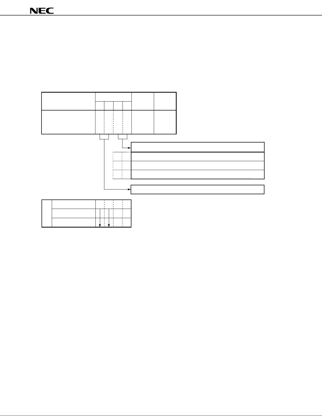
Table 7-2. Decimal Adjusted Data
µ
PD17072,17073
Result of
operation
10 0 1010B 1 0000B
11 0 1011B 1 0001B
12 0 1100B 1 0010B
13 0 1101B 1 0011B
14 0 1110B 1 0100B
15 0 1111B 1 0101B
16 1 0000B 1 0110B
17 1 0001B 1 0111B
18 1 0010B 1 1000B
19 1 0011B 1 1001B
20 1 0100B 1 1110B
21 1 0101B 1 1111B
22 1 0110B 1 1100B
23 1 0111B 1 1101B
24 1 1000B 1 1110B
25 1 1001B 1 1111B
26 1 1010B 1 1100B
27 1 1011B 1 1101B
28 1 1100B 1 1010B
29 1 1101B 1 1011B
30 1 1110B 1 1100B
31 1 1111B 1 1101B
Hexadecimal addition Decimal addition
CY
0 0 0000B 0 0000B
1 0 0001B 0 0001B
2 0 0010B 0 0010B
3 0 0011B 0 0011B
4 0 0100B 0 0100B
5 0 0101B 0 0101B
6 0 0110B 0 0110B
7 0 0111B 0 0111B
8 0 1000B 0 1000B
9 0 1001B 0 1001B
Result of
operation
CY
Result of
operation
Result of
operation
10 0 1010B 1 1100B
11 0 1011B 1 1101B
12 0 1100B 1 1110B
13 0 1101B 1 1111B
14 0 1110B 1 1100B
15 0 1111B 1 1101B
–16 1 0000B 1 1110B
–15 1 0001B 1 1111B
–14 1 0010B 1 1100B
–13 1 0011B 1 1101B
–12 1 0100B 1 1110B
–11 1 0101B 1 1111B
–10 1 0110B 1 0000B
– 9 1 0111B 1 0001B
– 8 1 1000B 1 0010B
– 7 1 1001B 1 0011B
– 6 1 1010B 1 0100B
– 5 1 1011B 1 0101B
– 4 1 1100B 1 0110B
– 3 1 1101B 1 0111B
– 2 1 1110B 1 1000B
– 1 1 1111B 1 1001B
Hexadecimal subtraction
CY
0 0 0000B 0 0000B
1 0 0001B 0 0001B
2 0 0010B 0 0010B
3 0 0011B 0 0011B
4 0 0100B 0 0100B
5 0 0101B 0 0101B
6 0 0110B 0 0110B
7 0 0111B 0 0111B
8 0 1000B 0 1000B
9 0 1001B 0 1001B
Result of
operation
Decimal subtraction
CY
Result of
operation
Remark The shaded part indicates that decimal adjustment is not made correctly.
43
Page 44

µ
PD17072,17073
7.4 Notes on Using ALU
7.4.1 Notes on executing operation to program status word
When an arithmetic operation is performed to the program status word, the result of the operation is stored in the
program status word.
The CY and Z flags of the program status word are usually set or reset according to the result of an arithmetic
operation executed. However, if the program status word itself is used for an operation, the result of the operation
is stored in the program status word, making it impossible to judge whether a carry or borrow occurs, or the result
of the operation is zero.
However, if the CMP flag is set, the result of the operation is not stored in the program status word; consequently,
the CY and Z flags are set (1) or cleared (0) normally.
7.4.2 Notes on using decimal operation
A decimal operation can be executed only if the result of the operation falls within the following range:
(1) Result of addition must be 0 to 19 in decimal.
(2) Result of subtraction must be 0 to 9 or –10 to –1 in decimal.
If a decimal operation is executed exceeding this range, the CY flag is set, and the result is 1010B (0AH) or higher.
44
Page 45

µ
PD17072,17073
8. PERIPHERAL CONTROL REGISTERS
8.1 Outline of Peripheral Control Registers
Figure 8-1 outlines the peripheral control registers.
Thirty-two 4-bit peripheral registers are available that control the peripheral hardware such as the PLL frequency
synthesizer, serial interface, and intermediate frequency counter (IF).
Because the peripheral control registers are located on the data memory, they can be manipulated by all the data
memory manipulation instructions.
Figure 8-1. Outline of Peripheral Control Registers
Column address
0123456789ABCDEF
0
BANK0
1
2
3
4
Row address
5
6
7
BANK1
Data memory
Peripheral control register
System registers
BCDEF
0
1
2
3
4
5
6
7
Peripheral hardware
45
Page 46

µ
PD17072,17073
8.2 Configuration and Function of Peripheral Control Registers
Figure 8-2 shows the configuration of the peripheral control registers.
Table 8-1 lists the peripheral hardware control functions of the peripheral control registers.
As shown in Figure 8-2, the peripheral control registers consist of a total of 32 nibbles (32 × 4 bits) of addresses
50H through 6FH of BANK1.
Each peripheral control register has an attribute of 1 nibble, and is classified into four types: read/write (R/W), read-
only (R), write-only (W), and read-and-reset (R&Reset) registers.
Nothing is changed even if data is written to the read only (R and R&Reset) registers.
If a write-only (W) register is read, the value is undefined.
Of the 4-bit data of 1 nibble, the bits fixed to “0” are always “0” when read, and also “0” when data is written to
these bits.
Caution Bit 3 of address 50H of BANK1 (bit 3 of the LCD driver display start register) is allocated to a test
mode area. Therefore, do not write “1” to this bit.
46
Page 47

[MEMO]
µ
PD17072,17073
47
Page 48

(BANK1)
Figure 8-2. Configuration of Peripheral Control Registers (1/2)
µ
PD17072,17073
Column address
Row
address
Item
Name
5
Symbol
Read/
Write
Name
6
Symbol
01234567
LCD driver
display
start register
Note
R/W R&Reset R R/W R/W R/W R/W R/W
Serial I/O
mode select
register
S
I
O
S
E
0
L
A
L
D
C
C
D
O
E
N00
N000
S
S
I
I
O
O
H
T
I
S
Z
Basic timer 0
carry register
Serial I/O
clock select
register
00
CE pin status
detection
register
B
T
M
0
CY000
IF counter
mode select
register
S
S
I
I
I
F
O
O
C
C
C
M
K
K
D
1
0
1
I
F
C
M
D
0
I
F
C
C
K
1
C
E
I
F
C
C
K
0
Port 1A
pull-down
resistor select
register
P
P
P
P
1
1
1
1
A
A
A
A
P
P
P
P
L
L
L
L
D
D
D
D
1
3
2
0
IF counter
gate status
detection
register
I
F
C
G
000
Stack pointer System clock
select register
S
S
P
P
1
0
00
IF counter
control
register
F
C
S
T
00
R
T
I
I
F
C
R
E
S
000
PLL
mode select
register
P
L
L
M
D
00
1
M
Interrupt edge
select
register
S
I
Y
N
S
T
C
K
0
PLL
reference
frequency
select register
P
P
L
L
L
L
R
D
0
F
0
C
K
2
B
T
M
1
C
K
P
L
L
R
F
C
K
1
Interrupt
enable
register
I
E
G
0
PLL
data register
P
P
L
L
L
L
R
R
F
1
C
7
K
0
I
P
S
I
O
P
L
L
R
1
6
I
P
B
T
M
1
P
L
L
R
1
5
I
P
P
L
L
R
1
4
Read/
Write
R/W R/W R/W R W R/W R/W R/W
Note This is a test mode area. Do not write “1” to this area.
48
Page 49

µ
PD17072,17073
Figure 8-2. Configuration of Peripheral Control Registers (2/2)
89ABCDEF
INT pin
interrupt
request
register
R/W R/W R/W R/W R/W R/W R/W R
P
P
L
L
L
L
R
R
1
1
2
3
Basic timer 1
interrupt
request
register
I
R
Q
000
P
P
P
L
L
L
L
L
L
R
R
R
1
1
9
1
0
Serial interface
interrupt request
register
I
R
Q
B
000
T
000
M
1
PLL data register PLL
P
P
P
P
L
L
L
L
R
R
7
8
P
L
L
L
L
L
L
R
R
R
6
5
4
R/W W R&Reset R/W R/W
BEEP clock
select register
I
R
Q
S
I
O
P
P
L
L
L
L
R
R
3
20
B
E
E
P
0
00
C
K
1
P
L
L
R
10 0 000
A/D converter
channel select
register
B
E
E
P
00
0
C
K
0
PLL data
set register
A
D
C
C
H
1
A
D
C
C
H
0
P
L
L
P
U
T
A/D converter
reference
voltage setting
register
A
A
A
A
D
D
D
D
C
C
C
C
R
R
R
R
F
F
F
F
S
S
S
S
E
E
E
E
L
L
L
L
0
2
3
1
unlock FF
register
P
L
L
U
000
L
A/D converter
compare start
register
Port 0B
bit I/O
select register
P
P
0
0
B
B
B
B
I
I
O
O
3
2
000
P
0
B
B
I
O
1
A
D
C
S
T
R
T
P
0
B
B
O
0
A/D converter
compare result
detection
register
Port 0C
bit I/O
select register
P
P
0
0
D
D
B
B
I
I
I
O
O
3
2
000
P
0
C
B
I
O
1
A
D
C
C
M
P
P
0
C
B
I
O
0
49
Page 50

µ
PD17072,17073
Table 8-1. Peripheral Hardware Control Functions of Peripheral Control Registers (1/4)
Peripheral Control register Peripheral hardware control function At reset
hardware Name Address Read/ b
3 Functional outline Set value
2 Symbol ON stop
Write b
b1
b0 01
Stack Stack pointer (BANK1) R/W 0 Fixed to 0 222
(SP) 54H 0
––––––––-
––––––––– ––––––––– ––––––––– –––––––– –
SP1 Stack pointer
– –––––––-
SP0
Timer Basic timer 0 (BANK1) R& 0 Fixed to 0 011
carry register 51H Reset 0
––––––––-
––––––––-
0
––––––––– ––––––––– ––––––––– ––––––––– ––––––––– ––––––––– ––––––
BTM0CY Detects status of carry FF Reset Set
Interrupt Interrupt edge (BANK1) R/W 0 Fixed to 0 000
select register 56H INT Detects status of INT Pin Low level High level
Interrupt enable (BANK1) R/W 0 Fixed to 0 000
register 57H IPSIO Serial interface Disables interrupt Enables interrupt
––––––––– ––––––––– ––––––––– ––––––––– ––––––––– ––––––––– ––––––
––––––––– ––––––––– ––––––––– ––––––––– ––––––––– ––––––––– ––––––
BTM1CK Sets set time interval of IRQBTM1 flag 32 ms (31.25 Hz) 8 ms (125 Hz)
––––––––– ––––––––– ––––––––– ––––––––– ––––––––– ––––––––– ––––––
IEG Sets interrupt issuing edge of INT pin
––––––––– ––––––––– ––––––––– ––––––––– ––––––––– ––––––––– ––––––
––––––––-
IPBTM1 Basic timer 1 Enables interrupt
––––––––-
Rising edge Falling edge
IP INT pin
INT pin interrupt (BANK1) R/W 0 Fixed to 0 000
request register 58H 0
––––––––-
––––––––-
0
––––––––– ––––––––– ––––––––– ––––––––– ––––––––– ––––––––– ––––––
IRQ Detects interrupt request of INT pin Not requested Requested
Basic timer 1 (BANK1) R/W 0 Fixed to 0 000
interrupt request 59H 0
register 0
––––––––-
––––––––-
––––––––– ––––––––– ––––––––– ––––––––– ––––––––– ––––––––– ––––––
IRQBTM1 Detects interrupt request of basic timer 1 Not requested Requested
Serial interface (BANK1) R/W 0 Fixed to 0 000
interrupt request 5AH 0
register 0
––––––––-
––––––––-
––––––––– ––––––––– ––––––––– ––––––––– ––––––––– ––––––––– ––––––
IRQSIO Detects interrupt of serial interface Not requested Requested
Pin CE pin status (BANK1) R 0 Fixed to 0 –––
detection register 52H 0
––––––––-
––––––––-
0
––––––––– ––––––––– ––––––––– ––––––––– ––––––––– ––––––––– ––––––
CE Detects status of CE pin Low level High level
Port 1A pull-down (BANK1) R/W P1APLD3 P1A3 Resistor ON Resistor OFF 0 R R
select register 53H P1APLD2 P1A2 Selects pull-down
–––––––––
–––––––––
P1APLD1 P1A1 resistor of these pins
–––––––––
P1APLD0 P1A0
Power-
Clock
CE
Remark –: Determined by status of pin, R: Previous status is retained.
50
Page 51

µ
PD17072,17073
Table 8-1. Peripheral Hardware Control Functions of Peripheral Control Registers (2/4)
Peripheral Control register Peripheral hardware control function At reset
hardware Name Address Read/ b
3 Functional outline Set value
2 Symbol ON stop
Write b
b1
b0 01
PLL PLL mode select (BANK1) R/W 0 Fixed to 0 00 R
frequency register 65H 0
synthesizer
PLL reference (BANK1) R/W 0 Fixed to 0 00R
frequency select 66H PLLRFCK2 Sets reference frequency of PLL
register PLLRFCK1
––––––––-
–––– ––––––––– ––––––––– ––––––––– ––––––––– ––––––––– ––––––––– –
PLLMD1 Sets division mode of PLL
–––––––– -
PLLMD0
–––– ––––––––– ––––––––– ––––––––– ––––––––– ––––––––– ––––––––– –
––––––––-
–––––––– -
0011
Disable MF VHF HF
0101
0:1 kHz 1:3 kHz 2:5 kHz
3:6.25 kHz 4:12.5 kHz
5:25 kHz 6, 7: PLL disable
PLLRFCK0
PLL data register (BANK1) R/W PLLR17 Sets division ratio of PLL U R R
67H PLLR16
–––– –––––
–––––––––
PLLR15
–––––––– –
PLLR14
(BANK1) PLLR13
68H PLLR12
–––– –––––
–––––––––
PLLR11
–––––––– –
PLLR10
(BANK1) PLLR9
69H PLLR8
–––– –––––
–––––––––
PLLR7
–––––––– –
• In direct division mode
PLLR6-PLLR17: Valid data
PLLR1-PLLR5: don’t care
0-15 (000H-00FH):
Setting prohibited
12
– 1 (010H-FFFH):
16-2
Can be set
Note
• In pulse swallow mode
PLLR1-PLLR17: Valid data
0-1023 (0000H-03FFH):
Setting prohibited
17
– 1 (0400H-1FFFFH):
1024-2
Can be set
Note
PLLR6
(BANK1) PLLR5
6AH PLLR4
–––– –––––
–––––––––
PLLR3
–––––––– –
PLLR2
(BANK1) PLLR1
6BH 0 Fixed to 0
–––– ––––– – – – –––– ––––– – – – –––– ––––– – – – –––– ––––– – – – –––– ––––– – – –
––––––––-
0
–––––––– -
0
PLL data set (BANK1) W 0 Fixed to 0 000
register 6CH 0
––––––––-
–––––––– -
0
–––– ––––– – – – –––– ––––– – – – –––– ––––– – – – –––– ––––– – – – –––– ––––– – – –
PLLPUT Data transfer to programmable counter Does not transfer Transfers
PLL unlock FF (BANK1) R& 0 Fixed to 0 URR
register 6DH Reset 0
––––––––-
–––––––– -
0
–––– ––––– – – – –––– ––––– – – – –––– ––––– – – – –––– ––––– – – – –––– ––––– – – –
PLLUL Detects status of unlock FF Locked status Unlocked status
Power-
Clock
CE
Note For the details of the set value, refer to Figure 15-4 Configuration of PLL Data Register.
Remark U: Undefined, R: Previous status is retained.
51
Page 52

µ
PD17072,17073
Table 8-1. Peripheral Hardware Control Functions of Peripheral Control Registers (3/4)
Peripheral Control register Peripheral hardware control function At reset
hardware Name Address Read/ b
3 Functional outline Set value
2 Symbol ON stop
Write b
b1
b0 01
A/D A/D converter (BANK1) R/W 0 Fixed to 0 000
converter channel select 5CH 0
register ADCCH1 Selects pin used for A/D converter
A/D converter (BANK1) R/W
reference 5DH
voltage setting
register
A/D converter (BANK1) R/W 0 Fixed to 0 000
compare start 5EH 0
register 0
A/D converter (BANK1) R 0 Fixed to 0 00 0
compare result 5FH 0
detection register 0
––––––––-
–––– ––––– – – – –––– ––––– – – – –––– ––––– – – – –––– ––––– – – – –––– ––––– – – –
–––––––– -
ADCCH0
ADCRFSEL3
–––– –––––
ADCRFSEL2
–––– –––––
Sets compare voltage 0 0 0
ADCRFSEL1
–––– –––––
ADCRFSEL0
––––––––-
–––––––– -
–––– ––––– – – – –––– ––––– – – – –––– ––––– – – – –––– ––––– – – – –––– ––––– – – –
ADCSTRT Invalid/Stop Starts/operates
––––––––-
–––––––– -
–––– ––––– – – – –––– ––––– – – – –––– ––––– – – – –––– ––––– – – – –––– ––––– – – –
Starts A/D converter operation/checks
comparator operation
0011
Not used AD0 AD1 AD1
0101
=x + 0.5
VREF
DD (V)
× V
16
(0 ≤ x ≤ 0FH)
ADCCMP Detects compare result VADCIN < VREF VADCIN > VREF
General- Port 0B bit I/O (BANK1) R/W P0BBIO3 P0B3 pin Input Output 0 0 0
purpose select register 6EH P0BBIO2 P0B2 pin
port P0BBIO1 P0B1 pin
–––– –––––
–––– –––––
–––– –––––
P0BBIO0 P0B0 pin Sets I/O mode of
Port 0C bit I/O (BANK1) R/W P0DBIO3 P0D3 pin these pins (bit I/O)
select register 6FH P0DBIO2 P0D2 pin
–––– –––––
–––– –––––
P0CBIO1 P0C1 pin
–––– –––––
P0CBIO0 P0C0 pin
Serial Serial I/O mode (BANK1) R/W 0 Fixed to 0 000
interface select register 60H SIOSEL
–––– ––––– – – – –––– ––––– – – – –––– ––––– – – – –––– ––––– – – – –––– ––––– – – –
–––– ––––– – – – –––– ––––– – – – –––– ––––– – – – –––– ––––– – – – –––– ––––– – – –
SIOHIZ Sets P1C0/SO0 pin in serial output mode Serial output
–––– ––––– – – – –––– ––––– – – – –––– ––––– – – – –––– ––––– – – – –––– ––––– – – –
SIOTS Sets start or stop of operation
Selects serial I/O mode of P0B3/SI/SO1 pin
Serial input Serial output
General-purpose
output port
Stops operation Starts operation
Serial I/O clock (BANK1) R/W 0 Fixed to 0 000
select register 61H 0
––––––––-
–––– ––––– – – – –––– ––––– – – – –––– ––––– – – – –––– ––––– – – – –––– ––––– – – –
SIOCK1 Sets clock of serial interface
–––––––– -
SIOCK0
0011
External clock
12.5 kHz 18.75 kHz 37.5 kHz
0101
Power-
Clock
CE
52
Page 53

µ
PD17072,17073
Table 8-1. Peripheral Hardware Control Functions of Peripheral Control Registers (4/4)
Peripheral Control register Peripheral hardware control function At reset
hardware Name Address Read/ b
3 Functional outline Set value
2 Symbol ON stop
Write b
b1
b0 01
IF counter IF counter mode (BANK1) R/W IFCMD1 Sets mode of IF counter 0 0 0
select register 62H IFCMD0
––––––––-
–––– ––––– – – – –––– ––––– – – – –––– ––––– – – – –––– ––––– – – – –––– ––––– – – –
IFCCK1 Sets gate time of IF counter
–––––––– -
IFCCK0
IF counter gate (BANK1) R 0 Fixed to 0 000
status detection 63H 0
register 0
IF counter control (BANK1) W 0 Fixed to 0 000
register 64H 0
––––––––-
–––––––– -
–––– ––––– – – – –––– ––––– – – – –––– ––––– – – – –––– ––––– – – – –––– ––––– – – –
IFCG
––––––––-
–––– ––––– – – – –––– ––––– – – – –––– ––––– – – – –––– ––––– – – – –––– ––––– – – –
IFCSTRT Starts counting of IF counter
–––– ––––– – – – –––– ––––– – – – –––– ––––– – – – –––– ––––– – – – –––– ––––– – – –
Detects opening/closing gate of IF counter
IFCRES Resets IF counter
BEEP BEEP clock (BANK1) R/W 0 Fixed to 0 00R
select register 5BH 0
––––––––-
–––– ––––– – – – –––– ––––– – – – –––– ––––– – – – –––– ––––– – – – –––– ––––– – – –
BEEP0CK1 Sets output status of BEEP pin
–––––––– -
BEEP0CK0
LCD LCD driver (BANK1) R/W 0 Fixed to 0
controller/ display start 50H 0
driver register ADCON
––––––––-
–––– ––––– – – – –––– ––––– – – – –––– ––––– – – – –––– ––––– – – – –––– ––––– – – – ––––––––––
Note
–––––––– - –––––––––––
Sets A/D converter power supply and 0 0 0
LCDEN ON/OFF of all LCD display 0 0 R
Standby System clock (BANK1) R/W 0 Fixed to 0 0RR
select register 55H 0
––––––––-
–––––––– -
0
–––– ––––– – – – –––– ––––– – – – –––– ––––– – – – –––– ––––– – – – –––– ––––– – – –
SYSCK 53.3
Selects system clock
(1 instruction execution time)
0011
IF counter OFF FMIFC pin AMIFC pin FMIFC pin
(General I/O port) FMIF mode AMIF mode AMIF mode
0101
0011
1 ms 4 ms 8 ms Open
0101
Closed Open
Does not start
Does not reset
0011
General output port General output port BEEP BEEP
(low-level output) (high-level output) (1.5 kHz) (3 kHz)
Starts
Resets
0101
0011
Power OFF Power ON Power ON Power ON
Display OFF Display ON Display OFF Display ON
0101
µ
s 106.6 µs
Power-
Clock
CE
Note When LCDEN= 1, the power supply for the A/D converter is ON even if ADCON = 0.
Remark R: Previous status is retained.
53
Page 54

9. DATA BUFFER (DBF)
9.1 General
Figure 9-1 outlines the data buffer.
The data buffer is located on the data memory and has the following two functions:
(1) Reads constant data on program memory (table reference)
(2) Transfers data with hardware peripherals
Figure 9-1. Outline of Data Buffer
Data buffer
Data write
(PUT instruction)
Table reference
(MOVT instruction)
µ
PD17072,17073
Constant data
Program memory
Data read (GET instruction)
Peripheral hardware
54
Page 55

µ
PD17072,17073
9.2 Data Buffer
9.2.1 Configuration of data buffer
Figure 9-2 shows the configuration of the data buffer.
As shown in this figure, the data buffer is configured of 16 bits of addresses 0CH-0FH of BANK0 on the data memory.
Of these 16 bits, bit 3 of address 0CH is the MSB, while bit 0 of address 0FH is the LSB.
Since the data buffer is on the data memory, it can be manipulated by all the data memory manipulation instructions.
Figure 9-2. Configuration of Data Buffer
Column address
00123456789ABCDEF
Data buffer
1
2
(DBF)
3
4
Row address
5
6
7
7
Data memory
Data buffer
Address
Bit
Bit
Symbol
Data
Data memory
BANK0
BANK1
System register
0CH
3 b2 b1 b0
b
b15 b14 b13 b12 b11 b10 b9 b8
DBF3
M
S
B
0DH
b3 b2 b1 b0 b3 b2 b1 b0 b3 b2 b1 b0
DBF2
Data
0EH
DBF1
0FH
b3 b2 b1 b0b7 b6 b5 b4
DBF0
L
S
B
55
Page 56

µ
PD17072,17073
9.2.2 Table reference instruction (“MOVT DBF, @AR”)
When this instruction is executed, the contents of the program memory addressed by the contents of the address
register are incorporated into the data buffer.
The program memory addresses to which table reference can be executed are addresses 0000H-0FFFH, i.e., all
the addresses of the program memory.
9.2.3 Peripheral hardware control instructions (“PUT” and “GET”)
The operations of the “PUT” and “GET” instructions are as follows:
(1) GET DBF, p
Reads the data of the peripheral register addressed by p to the data buffer.
(2) PUT p, DBF
Sets the data of the data buffer to the peripheral register addressed by p.
9.3 List of Peripheral Hardware and Data Buffer Functions
Table 9-1 lists the peripheral hardware and data buffer functions.
9.4 Notes on Using Data Buffer
When transferring data with the peripheral hardware through the data buffer, keep in mind the following three points
in respect with the unused peripheral addresses, write-only peripheral registers (only when using PUT), and readonly peripheral registers (only when using GET):
(1) An “undefined value” is read when a write-only register is read.
(2) Nothing is changed even when data is written to a read-only register.
(3) An “undefined value” is read when an unused address is read. Nothing is changed when data is written to
this address.
Table 9-1. Relation between Peripheral Hardware and Data Buffer
Peripheral Peripheral register transferring data with data buffer Function
hardware
Serial interface Presettable shift SIOSFR 03H PUT/ 8 8 Sets serial out data
Address register Address register AR 40H PUT/ 16 12 Transfers data with
(AR) GET address register
IF counter IF counter data IFC 43H GET 16 16 Reads count value of
Name Symbol Peripheral Execution No. of data No. of Outline
address of PUT/GET buffer I/O actual
instruction bits bits
register GET and reads serial in data
register IF counter
56
Page 57

µ
PD17072,17073
10. GENERAL-PURPOSE PORT
The general-purpose ports output high or low floating signals to external circuits, and reads high or low level signals
from external circuits.
10.1 General
Table 10-1 shows the relations between each port and port register.
The general-purpose ports are classified into I/O ports, input ports, and output ports.
The I/O port is the bit I/O ports, which can be set in the input or output mode in 1-bit (1-pin) units.
Table 10-1. Relations between Each Port (Pin) and Port Register
Port Pin Data setting method
No. Symbol I/O Port register (data memory) Remarks
56-pin 64-pin Bank Address Symbol Bit symbol
QFP TQFP (reserved word)
Port 0A 5 6 P0A3 Output BANK0 70H P0A b3 P0A3
Port 0B 56 64 P0B3 I/O 71H P0B b3 P0B3
Port 0C No pin 72H P0C b3 – Fixed to “0”
Port 0D 17 19 P0D3 I/O 73H P0D b3 P0D3
Port 1A 13 15 P1A3 Input BANK1 70H P1A b3 P1A3
Port 1B 9 10 P1B3 Output 71H P1B b3 P1B3
Port 1C No pin 72H P1C b3 –
––––––––– ––––––––– – -
4 4 P0A2 b2 P0A2
–––––––– ––––––––– –– -
3 3 P0A1 b1 P0A1
––––––– ––––––––– ––– -
––––––––– –––
–––––––– ––––
––––––– –––––
2 2 P0A0 b0 P0A0
––––––––– ––––––––– – -
55 63 P0B2 (bit I/O) b2 P0B2
–––––––– ––––––––– –– -
54 62 P0B1 b1 P0B1
––––––– ––––––––– ––– -
53 61 P0B0 b0 P0B0
––––––––– ––––––––– – –––––––– –
15 17 P0C1 I/O b1 P0C1
–––––––– –– ––––––– ––-
––––––––– –––
–––––––– ––––
––––––– –––––
––––––––– –––
b2 –
–––––––– ––––––––– –– –––––––––––––––––––
––––––– –––––
14 16 P0C0 (bit I/O) b0 P0C0
––––––––– – –––––––– –-
16 18 P0D2 (bit I/O) b2 P0D2
–––––––– –– ––––––– –––––––––––
No pin b1 – Fixed to “0”
––––––––– –––
–––––––– ––––––––– –– –––––––––––––––––––
––––––– –––––
b0 –
––––––––– ––––––––– – -
12 14 P1A2 b2 P1A2
–––––––– ––––––––– –– -
11 13 P1A1 b1 P1A1
––––––– ––––––––– ––– -
10 11 P1A0 b0 P1A0
––––––––– ––––––––– – -
8 9 P1B2 b2 P1B2
–––––––– ––––––––– –– -
7 8 P1B1 b1 P1B1
––––––– ––––––––– ––– -
6 7 P1B0 b0 P1B0
––––––––– ––––––––– – –––––––– –
1 1 P1C0 Output b0 P1C0
73H – b3 – Test mode area. Do not write
––––––––– –––
–––––––– ––––
––––––– –––––
––––––––– –––
–––––––– ––––
––––––– –––––
––––––––– –––
b2 – Fixed to “0”
––––––– –––––
b1 –
–––––––– ––––––––– –– –––––––––––––––––––
–––––
b2 “1” to this area.
–––––
b1
–––––
b0
57
Page 58

10.2 General-Purpose I/O Ports (P0B, P0C, P0D)
10.2.1 Configuration of I/O ports
The configurations of the I/O ports are shown below.
P0B (P0B3, P0B2, P0B1, P0B0)
P0C (P0C1, P0C0)
P0D (P0D3, P0D2)
µ
PD17072,17073
DD
V
V
DD
I/O mode selector flag
RESET
Output
latch
1
0
Write instruction
Port register
(1 bit)
Read instruction
10.2.2 Use of I/O ports
The I/O port is set in the input or output mode by the I/O select registers P0B and P0C of the control register.
P0D, P0C, and P0D are the bit I/O ports. Therefore, these ports can set in input or output mode in 1-bit units.
To set output data or to read input data, data is written to the corresponding port register, or an instruction that
reads the data is executed.
10.2.3 describes the configuration of the I/O select register of each port.
10.2.4 describes how to use an I/O port as an input port.
10.2.5 describes how to use an I/O port as an output port.
58
Page 59

µ
Name
Flag symbol
Address
Read/
Write
(BANK1)
6EH
R/W
Port 0B bit I/O
select register
0
1
0000
0
0
Power-ON
Clock stop
CE
Sets input or output mode
Sets P0B0 in input mode
b
3b2b1b0
0
1
0
1
0
1
P
0
B
B
I
O
3
000
000
P
0
B
B
I
O
2
P
0
B
B
I
O
1
P
0
B
B
I
O
0
Sets P0B0 in output mode
Sets input or output mode
Sets P0B1 in input mode
Sets P0B1 in output mode
Sets input or output mode
Sets P0B2/SCK in input mode
Sets P0B2/SCK in output mode
Sets input or output mode
Sets P0B3/SI/SO1 in input mode
Sets P0B3/SI/SO1 in output mode
At
reset
PD17072,17073
10.2.3 Control register of I/O port
The port 0B bit I/O select register sets the input or output mode of each pin of P0B. The port 0C bit I/O select register
sets the input or output mode of each pin of P0C and P0D.
The following paragraphs (1) and (2) describe the configuration and function.
(1) Port 0B bit I/O select register
59
Page 60

(2) Port 0C bit I/O select register
µ
PD17072,17073
Name
Port 0C bit I/O
select register
Flag symbol
3b2b1b0
b
P
P
0
D
B
I
O
2
0
1
P
0
C
B
I
O
1
0
1
0
D
B
I
O
3
Address
P
0
C
(BANK1)
B
6FH
I
O
0
0
Sets P0C0 pin in input mode
Sets P0C0 pin in output mode
1
Sets P0C1 pin in input mode
Sets P0C1 pin in output mode
Sets P0D2/AMIFC pin in input mode
Sets P0D2/AMIFC pin in output mode
Read/
Write
R/W
Sets input or output of port
Sets input or output of port
Sets input or output of port
At
reset
Power-ON
Clock stop
CE
0
1
0000
0
0
00
00
0
0
Sets input or output of port
Sets P0D3/FMIFC/AMIFC pin in input mode
Sets P0D3/FMIFC/AMIFC pin in output mode
60
Page 61

µ
PD17072,17073
10.2.4 To use I/O port in input mode
The port pin to be used in the input mode is selected by the I/O select register of each port.
The pin set in the input mode is floated (Hi-Z) and waits for the input of an external signal.
The input data can be read by executing a read instruction (such as SKT instruction) to the port register
corresponding to each pin.
“1” is read from the port register when the high level is input to the corresponding pin, and “0” is read from the register
when the low level is input to the pin.
If a write instruction (such as MOV instruction) is executed to the port register corresponding to a port set in the
input mode, the contents of the output latch are rewritten.
10.2.5 To use I/O Port in output mode
The port pin to be set in the output mode is selected by the I/O select register corresponding to the port.
The pin set in the output mode outputs the contents of the output latch.
The output data is set by executing a write instruction (such as MOV instruction) to the port register corresponding
to each pin.
To output the high level to each pin, “1” is written to the port register, and to output the low level, “0” is written.
The port pin can be floated (Hi-Z) by setting it in the input mode.
If a read instruction (such as SKT) is executed to the port register corresponding to a port set in the output mode,
the contents of the output latch are read.
10.2.6 I/O port status on reset
(1) On power-ON reset
All the ports are set in the input mode.
The contents of the output latch become 0.
(2) On CE reset
All the ports are set in the input mode.
The contents of the output latch are retained.
(3) On execution of clock stop instruction
All the ports are set in the input mode.
The contents of the output latch are retained.
Increasing current consumption can be prevented due to noise of the input buffer, by using the RESET signal,
as described in 10.2.1.
(4) In halt status
The previous status is retained.
61
Page 62

10.3 General-Purpose Input Ports (P1A)
10.3.1 Configuration of input ports
The configuration of the input ports is illustrated below.
P1A (P1A3, P1A2, P1A1, P1A0)
µ
PD17072,17073
High ON
resistance
To A/D converter
V
DD
P1APLD3
P1APLD2
P1APLD1
P1APLD0
RESET
Write instruction
Port register
(1 bit)
Read instruction
62
Page 63

µ
Flag symbol
b
3
P
1
A
P
L
D
3
b2
P
1
A
P
L
D
2
b1
P
1
A
P
L
D
1
b0
P
1
A
P
L
D
0
Name
Port 1A pull-down
resistor select register
Address
(BANK1)
53H
Read/
Write
R/W
Selects ON/OFF of pull-down resistor of P1A0 pin
Pull-down resistor ON
Pull-down resistor OFF
0
1
Selects ON/OFF of pull-down resistor of P1A1 pin
Pull-down resistor ON
Pull-down resistor OFF
0
1
Selects ON/OFF of pull-down resistor of P1A2/AD0 pin
Pull-down resistor ON
Pull-down resistor OFF
0
1
Selects ON/OFF of pull-down resistor of P1A3/AD1 pin
Pull-down resistor ON
Pull-down resistor OFF
0
1
Power-ON
Clock stop
CE
0000
Retained
Retained
At
reset
PD17072,17073
10.3.2 Using input port
The input data can be read by executing an instruction that reads the contents of the port register P1A (such as
SKT instruction).
“1” is read from each bit of the port register when the high level is input to the corresponding port pin, and “0” is
read when the low level is input.
Nothing is changed even if a write instruction (such as MOV) is executed to the port register.
Port 1A can be connected to or disconnected from a pull-down resistor bitwise by software. Whether the pull-down
resistor is connected or disconnected is specified by the port 1A pull-down resistor select register.
Figure 10-1 shows the configuration and function of the port 1A pull-down resistor select register.
Figure 10-1. Configuration of Port 1A Pull-Down Resistor Select Register
63
Page 64

10.3.3 Reset status of input port
(1) On power-ON reset
All pins are specified as a input port.
Pulled down internally.
(2) On CE reset
All pins are specified as a input port.
The previous status of the pull-down resistor is retained.
(3) On execution of clock stop instruction
All pins are specified as a input port.
The previous status of the pull-down resistor is retained.
(4) In halt status
The previous status is retained.
µ
PD17072,17073
64
Page 65

10.4 General-Purpose Output Ports (P0A, P1B, P1C)
10.4.1 Configuration of output ports
The configurations of the output ports are shown below.
P0A (P0A3, P0A2, P0A1, P0A0)
P1B (P1B3, P1B2, P1B1, P1B0)
P1C (P1C0)
V
DD
µ
PD17072,17073
Output
latch
10.4.2 Using output port
The output port outputs the contents of the output latch from its pins.
The output data is set by executing an instruction that writes data to the port register corresponding to each pin
(such as MOV instruction).
“1” is written to each bit of the port register when the high level is output to the corresponding port pin, and “0” is
written when the low level is output.
If a read instruction (such as SKT instruction) is executed to the port register, the contents of the output latch are
read.
10.4.3 Reset status of output port
Write instruction
Port register
(1 bit)
Read instruction
(1) On power-ON reset
All the pins output the contents of the output latch.
The contents of the output latch become 0.
(2) On CE reset
Retains the contents of the output latch.
The contents of the output latch are retained; therefore, the output data is not changed on CE reset.
(3) On execution of clock stop instruction
Retains the contents of the output latch.
The contents of the output latch are retained; therefore, the output data is not changed on execution of the
clock stop instruction.
Initialize the port through program as necessary.
(4) In halt status
The contents of the output latch are output.
The contents of the output latch are retained; therefore, the output data is not changed in the halt status.
65
Page 66

µ
PD17072,17073
11. INTERRUPT
11.1 General
Figure 11-1 shows the outline of the interrupt block.
As shown in this figure, the interrupt block temporarily stops the program under execution, and branches to an
interrupt vector address according to an interrupt request output by each peripheral hardware.
The interrupt block consists of “interrupt control blocks” that control interrupt requests output from the corresponding
peripheral hardware, “interrupt enable flip-flop” that enables all the interrupts, “stack pointer” that is controlled when
an interrupt is accepted, “address stack register”, “program counter”, and “interrupt stack”.
The “interrupt control block” of each peripheral hardware consists of an “interrupt request flag (IRQxxx)“ that detects
each interrupt, “interrupt enable flag (IPxxx)“ that enables each interrupt, and “vector address generator (VAG)“ that
specifies each vector address when an interrupt is accepted.
The following peripheral hardware have the interrupt functions:
• INT pin
• Basic timer 1
• Serial interface
Serial
interface
Basic
timer 1
Interrupt control block
IPSIO flag
IRQSIO flag
IPBTM1 flag
IRQBTM1 flag
IP flag
Figure 11-1. Outline of Interrupt Block
Vector address
generator 01H
Vector address
generator 02H
Stack pointer
Program counter
Address stack
register
Bank register
Interrupt stack
66
INT pin
IRQ flag
Vector address
generator 03H
DI, EI instruction
Interrupt enable
flip-flop
Page 67

µ
Name
INT pin
interrupt request
register
Flag symbol
b
3b2b1b0
0
I
R
Q
00
Address
Read/
Write
(BANK1)
58H
R/W
Sets interrupt request issuing status of INT pin.
Interrupt request not issued.
Interrupt request issued.
0
1
Fixed to "0".
Power-ON
Clock stop
CE
At
reset
0000
0
0
PD17072,17073
11.2 Interrupt Control Block
An interrupt control block is available for each peripheral hardware. Each of these blocks detects the presence/
absence of an interrupt request, enables/disables the interrupt, and generates a vector address when the interrupt
is accepted.
11.2.1 Interrupt request flag (IRQxxx)
The interrupt request flags are set to (1) when an interrupt request has been issued from the corresponding
peripheral hardware, and is cleared (0) when the interrupt has been accepted.
Therefore, even when the interrupt is not enabled, whether an interrupt request has been issued can be detected
by checking these interrupt request flags.
Writing “1” directly to an interrupt request flag is equivalent to issuance of an interrupt request.
Once this flag has been set, it will not be cleared until the corresponding interrupt has been accepted, or “0” is written
to the flag by an instruction.
If two or more interrupt requests are issued at the same time, the interrupt request flag corresponding to the interrupt
request that has not been accepted is not cleared.
The interrupt request flags are address 58H through 5AH of BANK1 of RAM.
Figures 11-2 through 11-4 show the configuration and functions of each interrupt request register.
Figure 11-2. Configuration of INT Pin Interrupt Request Register
67
Page 68

Figure 11-3. Configuration of Basic Timer 1 Interrupt Request Register
µ
PD17072,17073
Name
Basic timer 1
interrupt request
register
Power-ON
At
Clock stop
reset
CE
Flag symbol
b
3b2b1b0
I
R
Q
000
B
T
M
1
0
1
0000
0
0
Address
(BANK1)
59H
Interrupt request not issued.
Interrupt request issued.
Fixed to "0".
Read/
Write
R/W
Sets interrupt request issuing status of basic timer 1.
Name
Serial interface
interrupt request
register
Power-ON
At
Clock stop
reset
CE
Figure 11-4. Configuration of Serial Interface Interrupt Request Register
Flag symbol
b
3b2b1b0
I
R
Q
S
000
I
O
0
1
0000
0
0
Address
(BANK1)
5AH
Interrupt request not issued.
Interrupt request issued.
Fixed to "0".
Read/
Write
R/W
Sets interrupt request issuing status of serial interface.
68
Page 69
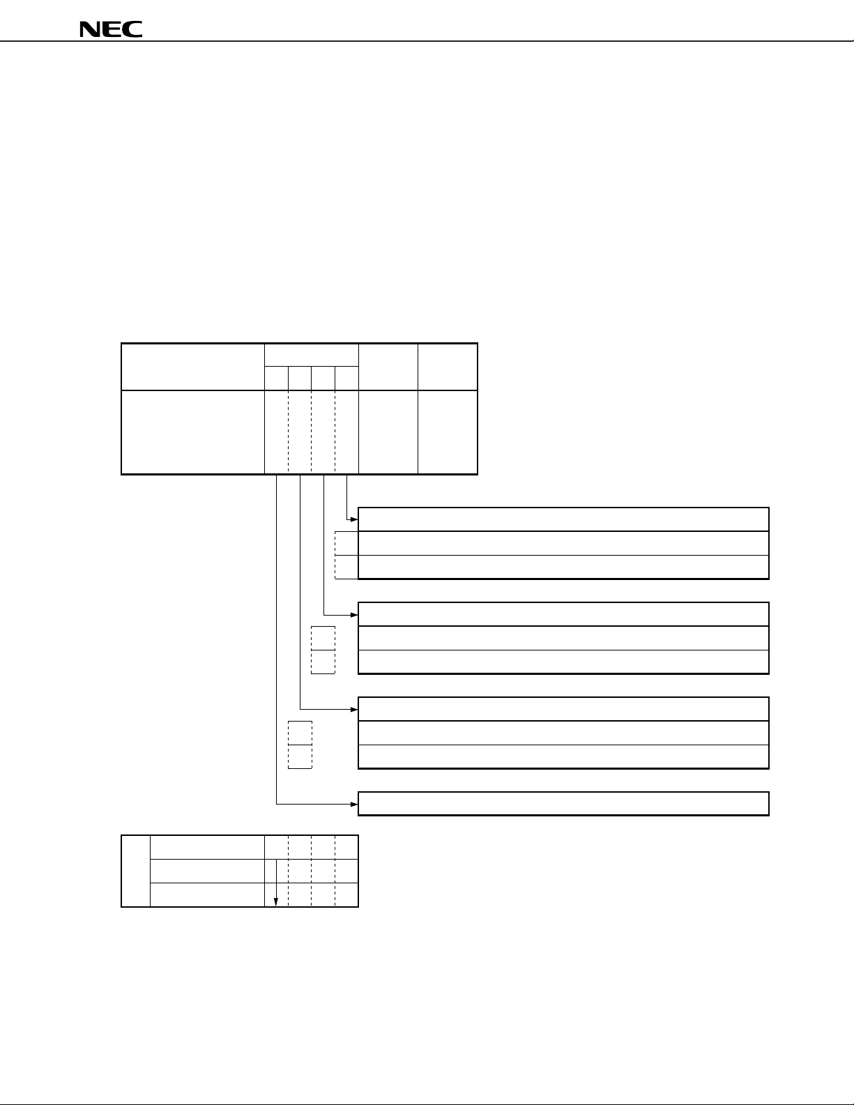
µ
Name
Flag symbol
Address
Read/
Write
(BANK1)
57H
R/W
I
P
Interrupt enable register
0
1
0000
0
0
Power-ON
Clock stop
CE
Enables interrupt from INT pin
Disables interrupt
Enables interrupt
b
3 b2 b1 b0
0
1
0
1
Enables interrupt from serial interface
Fixed to 0
I
P
B
T
M
1
I
P
S
I
O
0
00
00
Enables interrupt from basic timer 1
Disables interrupt
Enables interrupt
Disables interrupt
Enables interrupt
At
reset
PD17072,17073
11.2.2 Interrupt enable flag (IPxxx)
Each interrupt enable flag enables or disables the interrupt request of the corresponding peripheral hardware. So
that an interrupt is accepted, all the following three conditions must be satisfied:
• The interrupt must be enabled by the corresponding interrupt enable flag.
• The interrupt request must be issued from the corresponding interrupt request flag.
• The “EI” instruction (which enables all the interrupts) must be executed.
The interrupt enable flags are located on the interrupt enable registers on the register file.
Figure 11-5 shows the configuration and functions of the interrupt enable register.
Figure 11-5. Configuration of Interrupt Enable Register
69
Page 70

µ
PD17072,17073
11.2.3 Vector address generator (VAG)
When an interrupt request from peripheral hardware has been accepted, the vector address generator generates
a branch address (vector address) to which the program execution is to be branched.
The vector addresses corresponding to each interrupt source are listed in Table 11-1.
Table 11-1. Vector Address of Each Interrupt Source
Interrupt source Vector address
INT pin 03H
Basic timer 1 02H
Serial interface 01H
11.3 Interrupt Stack Register
11.3.1 Configuration and functions of interrupt stack register
Figure 11-6 shows the configuration of the interrupt stack register.
The interrupt stack saves the contents of the bank registers when an interrupt has been accepted:
When an interrupt has been accepted, and the contents of bank registers have been saved to the interrupt stack,
the contents of the registers are reset to “0”.
The interrupt stack can save up to one level of the contents of the bank registers; therefore, multiplexed interrupt
cannot be performed.
The contents of the interrupt stack register are restored to the respective system registers when an interrupt return
(“RETI”) instruction has been executed.
Caution With the
but retained when an interrupt is accepted. Therefore, the contents of the program status word
must be backed up by software.
µ
PD17073, the contents of the program status word (PSWORD) are not saved to the stack
Figure 11-6. Configuration of Interrupt Stack Register
Interrupt stack register (INTSK)
Name
Bit
0H
Bank stack
b
b
3
_
_
b
b
2
1
0
_
Remark –: Bit not saved
70
Page 71

µ
(
)
(
)
PD17072,17073
11.3.2 Operations of interrupt stack
Figure 11-7 illustrates the operations of the interrupt stack.
When multiplexed interrupts have been accepted, the first contents saved to the stack are popped. If these contents
are necessary, therefore, they must be saved through program.
Figure 11-7. Operations of Interrupt Stack
(a) If interrupt level does not exceed 1
Undefined
Application
of V
DD
Interrupt A
(BANK1)
(b) If interrupt level exceeds 1
BANK1
Interrupt A
BANK1
Interrupt B
BANK0
BANK1
BANK0
RETI
RETI
BANK1
BANK0
BANK0
RETI
71
Page 72

µ
PD17072,17073
11.4 Stack Pointer, Address Stack Register, and Program Counter
The address stack register saves the return address to which the program execution is to restore when execution
exits from an interrupt service routine.
The stack pointer specifies the address of the address stack register.
When an interrupt has been accepted, therefore, the value of the stack pointer is decremented by one, and the
value of the program counter at that time is saved to the address stack register specified by the stack pointer.
Next, when dedicated instruction “RETI” has been executed after the interrupt service routine has been executed,
the contents of the address stack register specified by the stack pointer are restored to the program counter, and the
value of the stack pointer is incremented by one.
Also refer to 3. ADDRESS STACK (ASK).
11.5 Interrupt Enable Flip-Flop (INTE)
The interrupt enable flip-flop enables all the interrupts.
When this flip-flop is set, all the interrupts are enabled. When it is reset, all the interrupts are disabled.
This flip-flop is set or reset by dedicated instruction “EI (set)” or “DI (reset)”.
The “EI” instruction sets this flip-flop when the instruction next to it has been executed, while the “DI” instruction
resets the flip-flop while it is executed.
When an interrupt has been accepted, this flip-flop is automatically reset.
This flip-flop is reset on power-ON reset, execution of the clock stop instruction, or CE reset.
72
Page 73

µ
PD17072,17073
11.6 Accepting Interrupt
11.6.1 Interrupt accepting operation and priority
An interrupt is accepted in the following sequence:
(1) Each peripheral hardware issues an interrupt request signal to an interrupt request block when a certain
condition is satisfied (for example, when a falling signal has been input to the INT pin).
(2) Each interrupt request block sets the corresponding interrupt request flag (e.g., IRQ flag for the INT pin) to
“1” when it has received an interrupt request signal from peripheral hardware.
(3) When the interrupt request flag is set, the interrupt request block whose interrupt enable flag (e.g., IP flag for
IRQ flag) is set to “1” outputs “1”.
(4) The signal output by the interrupt request block is ORed with the output of the interrupt enable flip-flop and
an interrupt accept signal is output.
This interrupt enable flip-flop can be set to “1” by the EI instruction and reset to “0” by the DI instruction.
When “1” is output from an interrupt request block with the interrupt enable flip-flop set to “1”, the interrupt
enable flip-flop outputs “1” and the interrupt is accepted.
When the interrupt has been accepted, the output of the interrupt enable flip-flop is input to the block that has issued
the interrupt request, through an AND circuit, as shown in Figure 11-1.
The signal input to the block that has issued the interrupt request clears the interrupt request flag of that block to
“0”, and a vector address corresponding to the interrupt is output.
If any of the blocks that have issued an interrupt request outputs “1” at this time, the interrupt accept signal is not
transmitted to the next stage. When two or more interrupt request have generated at the same time, therefore, the
interrupts are accepted according to the following priority:
INT pin > basic timer 1 > serial interface
The interrupt corresponding to an interrupt source is not accepted unless the interrupt enable flag is set to “1”.
Therefore, by clearing the interrupt enable flag to “0”, an interrupt with a high hardware priority can be disabled.
73
Page 74

µ
PD17072,17073
11.6.2 Timing to accept interrupt
Figure 11-8 is a timing chart illustrating how interrupts are accepted.
(1) in this figure illustrate how one type of interrupt is accepted.
(a) in (1) indicates the case where the interrupt request flag is set to “1” last, while (b) shows the case where
the interrupt enable flag is set to “1” last.
In either case, the interrupt is accepted after all the interrupt request flag, interrupt enable flip-flop, and interrupt
enable flag have been set.
If it is during the first instruction cycle of the “MOVT DBF, @AR” instruction or an instruction with the skip condition
satisfied that sets the last flag or flip-flop to “1”, the interrupt is accepted during the second instruction cycle of the
“MOVT DBF, @AR” instruction or when the skipped instruction (“NOP”) has been executed.
The interrupt enable flip-flop is set in the instruction cycle next to the one in which the “EI” instruction is executed.
(2) in Figure 11-8 shows the timing chart where two or more interrupts are used.
When using two or more interrupts, the interrupt given the highest hardware priority at that time is accepted if all
the interrupt enable flags are set. However, the hardware priority can be changed by manipulating the interrupt enable
flag through program.
“Interrupt cycle” in Figure 11-8 is a special cycle in which the interrupt request flag is clear, a vector address is
specified, and the contents of the program counter are saved after an interrupt has been accepted, and lasts for 53.3
µ
s, (normal operation) or one instruction execution time.
For details, refer to 11.7 Operations after Accepting Interrupt.
74
Page 75

Figure 11-8. Interrupt Accepting Timing Chart (1/2)
(1) When one type of interrupt (e.g., rising edge of INT pin) is used
(a) When there is no time to mask interrupt by interrupt enable flag (IPxxx)
If an ordinary instruction which is not “MOVT” or does not satisfy the skip condition
<1>
is executed when interrupt is accepted
µ
PD17072,17073
Instruction EI
INTE
INT pin
IRQ flag
IP flag
1 instruction cycle
(normal operation)
If “MOVT” or an instruction that satisfies the skip condition is executed when
<2>
interrupt is accepted
Instruction EI
INTE
INT pin
53.3 s
µ
MOV
WR, #0001B
MOV
WR, #0001B
POKE
INTPM1, WR
POKE
INTPM1, WR
Ordinary
instruction
Interrupt enable period
MOVT DBF,@AR
skip instruction
Interrupt
cycle
service routine
Interrupt accepted
Interrupt
cycle
Interrupt
IRQ flag
IP flag
Interrupt enable period
(b) When there is interrupt pending time by interrupt enable flag
Instruction EI
INTE
INT pin
IRQ flag
IP flag
MOV
WR, #0001B
Interrupt pending period
POKE
INTPM1, WR
Interrupt accepted
Interrupt
cycle
service routine
Interrupt accepted
Interrupt
Interrupt
service routine
75
Page 76

Figure 11-8. Interrupt Accepting Timing Chart (2/2)
(2) When two or more interrupts are used (e.g., INT pin and basic timer 1)
(a) Hardware priority
µ
PD17072,17073
Instruction
INTE
INT pin
IRQ flag
Basic timer 1
IRQBTM1 flag
IP flag
IPBTM1 flag
(b) Software priority
Instruction
MOV
WR, #0011B
MOV
WR, #0010B
POKE
INTPM1, WR
INT pin interrupt pending period
POKE
INTPM1, WR
EI EI
EI
Interrupt
cycle
INT pin interrupt service routine
RETI
Basic timer 1 interrupt pending period
INT pin interrupt accepted
Interrupt
cycle
MOV
WR, #0011B
POKE
INTPM1, WR
Interrupt
Note
cycle
Basic timer 1
interrupt service
Basic timer 1 interrupt accepted
Note
RETI
EI
Interrupt
cycle
INTE
INT pin
IRQ flag
Basic timer 1
IRQBTM1 flag
IP flag
IPBTM1 flag
INT pin interrupt pending period
Basic timer 1 interrupt pending period
Basic timer 1 interrupt service routine
Basic timer 1 interrupt accepted
Note Because the level of the interrupt stack is 1, multiplexed interrupt cannot be performed.
INT pin interrupt
service
INT pin interrupt
accepted
76
Page 77

µ
PD17072,17073
11.7 Operations after Accepting Interrupt
When an interrupt has been accepted, the following processing is automatically executed in sequence:
(1) The interrupt enable flip-flop and the interrupt request flag corresponding to the accepted interrupt request
are cleared to “0”. Therefore, the interrupt is disabled.
(2) The contents of the stack pointer are decremented by one.
(3) The contents of the program counter are saved to the address stack register specified by the stack pointer.
At this time, the content of the program counter is the program memory address next to the one at which the
interrupt has been accepted.
For example, if the interrupt has been accepted while a branch instruction is executed, the branch destination
address is loaded to the program counter. If a subroutine call instruction is executed when the interrupt has
been accepted, the address that called the subroutine is loaded to the program counter. When the skip
condition of a skip instruction is satisfied, the next instruction is treated as a no-operation instruction (“NOP”)
and then the interrupt is accepted. Consequently, the contents of the program counter are the skipped address.
(4) The lower 1 bit of the bank register (BANK) is saved to the interrupt stack.
Caution At this time, the contents of the program status word (PSWORD) are not saved. Save the
contents of the program status word by software as necessary.
(5) The contents of the vector address generator corresponding to the accepted interrupt are transferred to the
program counter. Therefore, the execution branches to an interrupt service routine.
µ
The above steps (1) through (5) are executed in one special instruction cycle (53.3
not involve execution of an ordinary instruction. This instruction cycle is called an interrupt cycle.
Therefore, it takes the CPU one instruction cycle to branch to the corresponding vector address after it has accepted
an interrupt.
s: normal operation) that does
77
Page 78

µ
PD17072,17073
11.8 Exiting from Interrupt Service Routine
To return to the service that was executed when the interrupt was accepted from the interrupt service routine, a
dedicated instruction “RETI” is used.
When this instruction is executed, the following processing is automatically executed in sequence:
(1) The contents of the address stack register specified by the stack pointer are restored to the program counter.
(2) The contents of the interrupt stack are restored to the lower 1 bit of the bank register (BANK).
Caution If the contents of the program status word are saved in the program, its contents must be
restored to the program status word at the same time.
(3) The contents of the stack pointer are incremented by one.
The processing (1) through (3) above is executed in one instruction cycle during which the “RETI” instruction is
executed.
The only difference between the “RETI” and subroutine return instructions “RET” and “RETSK” is the restore
operation of each system register described in step (2) above.
78
Page 79

µ
PD17072,17073
11.9 External (INT Pin) Interrupts
11.9.1 Outline of external interrupts
Figure 11-9 outlines the external interrupts.
As shown in this figure, an interrupt request for an external interrupt is issued at the rising or falling edge of the
signal input to the INT pin.
Whether the interrupt request is to be issued at the rising or falling edge of INT is specified independently through
program.
The INT pin is Schmitt trigger input pin to protect malfunctioning due to noise. This pin do not accept a pulse input
that lasts for less than 100 ns.
Figure 11-9. Outline of External Interrupt
INT flag
INT pin
Schmitt trigger
Remark INT: detects pin status
IEG: selects interrupt edge
11.9.2 Edge Detection Block
The edge detection block specifies the edge (rising or falling edge) of the input signal that issues the external
interrupt request of the INT pin, and detects the specified edge.
The edge is specified by IEG flag.
Figure 11-10 shows the configuration and function of the interrupt edge select register.
IEG flag
Edge
detection
block
Interrupt control block
IRQ flag
79
Page 80

Figure 11-10. Configuration of Interrupt Edge Select Register
µ
PD17072,17073
Name Address
Interrupt edge select
register
Flag symbol
3
2
b
b
I
N
T
0
Read/
b
b
1
0
B
I
T
E
M
G
(BANK1)
1
C
K
0
1
56H
Rising edge
0
Falling edge
1
32 ms (31.25 Hz)
8 ms (125 Hz)
Write
R/W
Sets input edge to issue interrupt request of INT pin
Sets time interval at which IRQBTM1 flag is set
Note
Detects status of INT pin
Low level is input to INT pin
High level is input to INT pin
Fixed to “0”
0
0
0
At
reset
Power-ON
Clock stop
CE
0
1
0
0
0
0
0
0
0
Note For the function of the BTM1CK flag, refer to 12.3.1 Outline of basic timer 1.
Note that as soon as the interrupt request issuing edge is changed by the IEG flag, the interrupt request signal
may be issued.
Suppose that the IEG flag is set to “1” (specifying the falling edge) and that a high level is input to the INT pin, as
shown in Table 11-2. If the IEG flag is cleared at this time, the edge detector circuit judges that a rising edge has
been input, and issues an interrupt request.
80
Page 81

µ
Table 11-2. Issuing Interrupt Request By Changing IEG Flag
PD17072,17073
Changes in IEG flag
1 → 0
(falling) (rising)
0 → 1
(rising) (falling)
11.9.3 Interrupt control block
The level of a signal input to the INT pin can be detected by using the INT flag.
This flag is set or cleared independently of interrupts; therefore, it can be used as a 1-bit general-purpose input
port when the interrupt function is not used.
The INT flag can also be used as a general-purpose port that can detect the rising or falling edge by reading an
interrupt request flag if the interrupt corresponding to the flag is not enabled.
In this case, however, the interrupt request flag is not automatically cleared and must be cleared by program.
Also refer to Figure 11-10.
INT pin status Interrupt request
Low level Not issued Retains previous status
High level Issued Set to “1”
Low level Issued Set to “1”
High level Not issued Retains previous status
IRQ flag status
11.10 Internal Interrupt
Two internal interrupt sources, basic timer 1, and serial interface, are available.
11.10.1 Interrupt by basic timer 1
This interrupt request is issued at fixed time intervals.
For details, refer to 12. TIMER.
11.10.2 Interrupt by serial interface
This interrupt request is issued when a serial output or serial input operation has been completed.
For details, refer to 14. SERIAL INTERFACE.
81
Page 82

µ
PD17072,17073
12. TIMER
The timers are used to control the program execution time.
12.1 General
As shown in this figure, the µPD17013 is provided with the following two timers:
• Basic timer 0
• Basic timer 1
The basic timer 0 is used to detect the status of a flip-flop that is set at fixed time intervals.
The basic timer 1 is used to issue an interrupt request at fixed time intervals.
The basic timer 0 can also be used to detect a power failure. The clock of each timer is generated by dividing the
system clock (75 kHz).
12.2 Basic Timer 0
12.2.1 General
Figure 12-1 outlines the basic timer 0.
The basic timer 0 is used as a timer by detecting the status of a flip-flop which is set at fixed time intervals, by using
the BTM0CY flag (BANK1 of RAM: address 51H, bit 0).
The content of the flip-flop corresponds to the BTM0CY flag on a one-to-one basis.
The set time for BTM0CY flag (BTM0CY flag set pulse) is 125 ms (8 Hz).
If the BTM0CY flag is read for the first time after power-ON reset, its content is always “0”. After that, the flag is
set to “1” at fixed time intervals.
If the CE pin goes high, CE reset is effected when the BTM0CY flag is set next time.
By reading the content of the BTM0CY flag at system reset (power-ON reset and CE reset), therefore, a power
failure can be detected.
For details on power failure detection, refer to 20. RESET.
Figure 12-1. Outline of Basic Timer 0
75 kHz
Remark BTM0CY (bit 0 of basic timer 0 carry register: refer to Figure 12-2) detects the status of the flip-flop.
Divider
125 ms (8 Hz)
Basic timer
0 carry FF
Set/clear
BTM0CY flag
82
Page 83

µ
PD17072,17073
12.2.2 Flip-flop and BTM0CY flag
The flip-flop is set at fixed time intervals and its status is detected by the BTM0CY flag of the basic timer 0 carry
register.
The BTM0CY flag is a read-only flag, and is reset to “0” if its contents are read (Read & Reset) by using the
instructions shown in Table 12-1.
The BTM0CY flag is reset to “0” at power-ON reset, and is set to “1” at CE reset and at CE reset after the clock
stop instruction is executed. Therefore, this flag can be used as a power failure detection flag.
The BTM0CY flag is not set until its contents are read by the instruction shown in Table 12-1 after application of
the supply voltage. Once a read instruction has been executed, this flag is set at fixed time intervals.
Figure 12-2 shows the configuration and function of the basic timer 0 carry register.
Table 12-1. Instructions to Reset BTM0CY Flag
Mnemonic Operand Mnemonic Operand
ADD m, #n4 ADD r, m
ADDC ADDC
SUB SUB
SUBC SUBC
AND AND
OR OR
XOR XOR
SKE LD
SKEG SKT m, #n
SKLT SKF
SKNE MOV @r, m
Note
m, @r
Note When the row address of m is 5H and 1H is written to r.
Remark m = 51H
83
Page 84

Figure 12-2. Configuration of Basic Timer 0 Carry Register
µ
PD17072,17073
Name
Basic timer 0 carry register
Power-ON
At
Clock stop
reset
CE
Flag symbol
3b2b1b0
b
000
0000
1
1
B
T
M
0
C
Y
Address
(BANK1)
51H
Flip-flop is not set.0
Flip-flop is set.1
Fixed to "0".
Read/
Write
R&Reset
Detects status of flip-flop.
12.2.3 Application example of basic timer 0
An example of a program in which the basic timer 0 is used is shown below.
In this example, processing A is executed every 1 second.
Example
M1 MEM 1.10H ; 1-second counter, set to bank 1
LOOP:
BANK1
SKT1 BTM0CY ; Branches to NEXT if BTM0CY flag is “0”
BR NEXT
ADD M1, #0010B ; Adds 2 to M1
SKT1 CY ; Executes processing A if CY flag is “1”
BR NEXT ; Branches to NEXT if CY flag is “0”
Processing A
NEXT:
Processing B
BR LOOP ; Executes processing B and branches to LOOP
84
Page 85

µ
PD17072,17073
12.2.4 Error of basic timer 0
The time at which the BTM0CY flag is to be detected must be shorter than the time at which the BTM0CY flag is
to be set (refer to 12.2.5 Notes on using basic timer 0).
Where the time interval at which the BTM0CY flag is to be detected is t
CHECK and the time interval at which the
BTM0CY flag is to be set (125 ms) is tSET, the relation between tCHECK and tSET must be as follows:
CHECK < tSET
t
At this time, as shown in Figure 12-3, the timer error when the BTM0CY flag is detected is:
0 < error < tSET
Figure 12-3. Error of Basic Timer 0 due to Detection Time of BTM0CY Flag
BTM0CY flag
setting pulse
BTM0CY flag
H
L
t
SET
1
0
t
CHECK1
SKT1
BTM0CY
<1>
SKT1
BTM0CY
<2>
t
CHECK2
SKT1
BTM0CY
<3>
t
CHECK3
SKT1
BTM0CY
<4>
As shown in Figure 12-3, the timer is updated because the BTM0CY flag is detected as “1” in <2>.
In <3>, the flag is “0”; therefore, the timer is not updated until the BTM0CY flag is detected again in <4>.
At this time, the time of the timer is extended by t
CHECK3.
85
Page 86

12.2.5 Notes on using basic timer 0
(1) BTM0CY flag detection time interval
The time interval at which the BTM0CY flag is to be detected must be shorter than the time interval at which
the flag is to be set. This is because, if the time of processing B in Figure 12-4 is longer than the time interval
at which the BTM0CY flag is to be set, the BTM0CY flag is not set accurately.
Figure 12-4. Detection of BTM0CY Flag and BTM0CY Flag
µ
PD17072,17073
BTM0CY flag
setting pulse
BTM0CY flag
H
L
1
0
<1>
SKT1
BTM0CY
Because execution time of processing B is too long after BTM0CY
flag, which has been set to "1" in step <2> above, has been
detected, BTM0CY flag is not detected in step <3>.
<2> <3>
SKT1
BTM0CY
Processing A
Processing B
<4>
SKT1
BTM0CY
<5>
(2) Sum of timer updating processing time and BTM0CY flag detection time interval
As described in (1) above, the time interval tCHECK at which the BTM0CY flag is to be detected must be shorter
than the time at which the BTM0CY flag is to be set.
At this time, even if the time interval at which the BTM0CY flag is to be detected is short, the timer processing
may not be executed normally when CE reset is effected if the updating processing time of the timer is long.
Therefore, the following conditions must be satisfied:
86
CHECK + tTIMER < tSET
t
where,
tCHECK: time interval at which BTM0CY flag is detected
TIMER: timer updating processing time
t
tSET: time interval at which BTM0CY flag is set
An example is shown below.
Page 87

µ
PD17072,17073
Example Timer updating processing and BTM0CY flag detection time interval
BTIMER:
BANK1
SKT1 BTM0CY ; Executes timer updating processing if BTM0CY flag is “1”.
BR AAA ; Branches to AAA if BTM0CY flag is “0”.
Timer updating
BR BTIMER
AAA:
Processing A
BR BTIMER
The following is the timing chart of the above program.
CE pin
BTM0CY flag
setting pulse
BTM0CY flag
H
L
H
L
1
0
BTM0CY detection
interval
t
CHECK
SKT1
BTM0CY
SKT1
BTM0CY
Timer updating
processing
TIMER
t
If this timer updating processing time is
too long, CE reset is effected while
processing is in progress.
CE reset
87
Page 88

µ
PD17072,17073
(3) Adjusting basic timer 0 at CE reset
An example of adjusting the basic timer 0 at CE reset is shown on the next page.
As shown in this example, the timer may have to be adjusted if the BTM0CY flag is used for power failure
detection and, at the same time, the flag is used for a watch timer.
When the power is applied the first time (power-ON reset), the BTM0CY flag is cleared to “0”, and not set until
the contents of the flag is read again by an instruction shown in Table 12-1.
If the CE pin goes high, CE reset is effected in synchronization with rising edge of the BTM0CY flag setting
pulse. At this time, the BTM0CY flag is set to “1” and starts.
Therefore, it can be judged, when system reset (power-ON reset or CE reset) has been effected, whether the
system reset is power-ON reset or CE reset, by checking the status of the BTM0CY flag.
That is, if the BTM0CY flag is “0”, power-ON reset has been effected; if the flag is “1”, CE reset has been effected
(for power failure detection).
At this time, the watch timer must continue its operation even when CE reset has been effected.
However, because the BTM0CY flag is cleared to “0” as a result of reading the BTM0CY flag to detect a power
failure, the set (1) status of the BTM0CY flag is overlooked once.
Consequently, it is necessary to update the watch timer if CE reset has been detected as a result of power
failure detection.
For details on power failure detection, refer to 20.6 Power Failure Detection.
Example Adjusting timer at CE reset (to detect power failure and update watch by BTM0CY flag)
START: ; Program address 0000H
Processing A
; <1>
BANK1
SKT1 BTM0CY ; Embedded macro
; Tests BTM0CY flag.
BR INITIAL ; If BTM0CY is “0”, branches to INITIAL (power failure detection).
BACKUP:
; <2>
Updates watch 125 ms.
LOOP:
; <3>
Processing B ; While performing processing B,
SKF1 BTM0CY ; tests BTM0CY flag and updates watch.
BR BACKUP
BR LOOP
INITIAL:
Processing C ; Initialization of ports and peripheral hardware.
BR LOOP
; Adjusts watch because this is back up (CE reset)
88
Figure 12-5 shows the timing chart of the above program.
Page 89

Figure 12-5. Timing Chart
µ
PD17072,17073
V
DD
CE
Internal pulse
8 Hz
BTM0CY flag
setting pulse
BTM0CY flag
Program processing
Program instruction
Power application
As shown in Figure 12-5, the program is started from address 0000H in synchronization with the rising of the
internal 8-Hz pulse when supply voltage V
When the BTM0CY flag is detected next at point A, the BTM0CY flag is cleared to 0 because power has been
just applied. It is therefore judged that a power failure (i.e., power-ON reset) has been detected, and
“processing C” is executed.
Because the content of the BTM0CY flag has been read once at point A, the BTM0CY flag is set to 1 every
125 ms afterward.
Next, even if the CE pin goes low at point B and goes high at point C, the program executes “processing B”
and increments the watch, unless the clock stop instruction is executed.
Because the CE pin goes high at point C, CE reset is effected at point D where the BTM0CY flag setting pulse
rises, and the program is started from address 0000H.
At this time, if the BTM0CY flag is detected at point E, it is judged that back up (CE reset) has been effected,
because the BTM0CY flag is set to 1.
As is evident from the above figure, the watch is delayed by 125 ms each time CE reset is effected, unless
the watch is updated 125 ms at point E.
If processing A takes 125 ms or longer when a power failure is detected at point E, setting of the BTM0CY
flag is overlooked two times; therefore, processing A must be completed within 125 ms.
Therefore, the BTM0CY flag must be detected for a power failure detection within the BTM0CY flag setting
time after the program has been started from the address 0000H.
3 V
0 V
H
L
H
L
H
L
1
0
Power-ON reset starts
from address 0.
AC B B B BB B B B BBBABB
Watch UP Watch UP Watch UP Watch UP Watch UP
CE reset starts
from address 0.
BTM0CY flag detection
Point A Point B Point C Point D Point E
DD is applied first.
<3><3><1><3><3><3> <3><3><3><3><3><3><3><1>
BTM0CY flag is detected.
Time updated because
flag is set to 1.
89
Page 90

µ
PD17072,17073
(4) If detection of BTM0CY flag overlaps with CE reset
As described in (3), the CE reset is effected as soon as the BTM0CY flag has been set to 1.
If the BTM0CY flag read instruction happens to be executed at the same time as the CE reset, the BTM0CY
flag read instruction takes precedence.
Therefore, if setting of the BTM0CY flag after the CE pin has gone high overlaps with the BTM0CY flag read
instruction, the CE reset is effected when “the BTM0CY flag is set next time”.
This operation is illustrated in Figure 12-6.
Figure 12-6. Operation when CE Reset and BTM0CY Flag Read Instruction Overlap
CE pin
BTM0CY flag
setting pulse
BTM0CY flag
BTM0CY flag
setting pulse
BTM0CY flag
Instruction
H
L
H
L
1
0
SKT 1
BTM0CY
H
L
1
0
SKT 1
BTM0CY
SKT1 BTM0CY
53.3 s
Originally, program starts from address 0000H here.
However, because it happens to overlap with a
program that reads BTM0CY, CE reset is not effected.
CE reset
Embedded macro
SKT .MF. BTM0CY SHR4,
µ
#.DF. BTM0CY AND 0FH
If BTM0CY flag is read during
this period, CE is delayed.
In a program that cyclically detects the BTM0CY flag, in which the BTM0CY flag detection time interval
coincides with the BTM0CY flag setting time, CE reset is never effected.
90
Page 91

µ
PD17072,17073
12.3 Basic Timer 1
12.3.1 General
Figure 12-7 outlines the basic timer 1.
The basic timer 1 issues an interrupt request at fixed time interval and sets the IRQBTM1 flag to 1.
The time interval of the IRQBTM1 flag is set by the BTM1CK flag of the interrupt edge select register. Figure 12-
8 shows the configuration and function of the interrupt edge select register.
The interrupt generated by the basic timer 1 is accepted when the IRQBTM1 flag is set, if the EI instruction has
been issued and the IPBTM1 flag has been set (refer to 11. INTERRUPT).
Figure 12-7. Outline of Basic Timer 1
BTM1CK flag
Internal signal
75 kHz
(fixed)
Remark BTM1CK (bit 1 of interrupt edge select register. Refer to Figure 12-8) set the time interval at which the
IRQBTM1 flag is set.
Divider
32 ms (31.25 Hz)
8 ms (125 Hz)
Selector
IRQBTM1 set signal
91
Page 92

Figure 12-8. Configuration of Interrupt Edge Select Register
µ
PD17072,17073
Name Address
Interrupt edge
select register
Flag symbol
b
3
2
b
I
N
T
0
0
1
Read/
b
b
1
0
B
I
T
E
M
G
(BANK1)
1
C
K
0
1
56H
Rising edge
0
Falling edge
1
32 ms (31.25 Hz)
8 ms (125 Hz)
Low level is input to INT pin.
High level is input to INT pin.
Write
R/W
Sets input edge to issue interrupt request of INT pin
Sets time interval at which IRQBTM1 flag is set
Detects status of INT pin
Note
Note
Fixed to “0”.
0
0
0
0
0
0
0
0
0
0
At
reset
Power-ON
Clock stop
CE
Note For the functions of IEG and INT flags, refer to 11.9 External (INT pin) Interrupt.
92
Page 93

µ
PD17072,17073
12.3.2 Application example of basic timer 1
A program example is shown below.
Example
M1 MEM 0.10H ; 80-ms counter
BTIMER1 DAT 0002H ; Symbol definition of basic timer 1 interrupt vector address
BR START ; Branches to START
ORG BTIMER1 ; Program address (0002H)
ADD M1, #0001B ; Adds 1 to M1
SKT1 CY ; Tests CY flag
BR EI_RETI ; Returns if no carry
MOV M1, #0110B
Processing A
EI_RETI:
EI
RETI
START:
MOV M1, #0110B ; Initializes contents of M1 to 6
BANK1
SET1 BTM1CK ; Embedded macro
; Sets basic timer 1 interrupt pulse to 8 ms
SET1 IPBTM1 ; Enables basic timer 1 interrupt
EI ; Enables all interrupts
LOOP:
BANK0
Processing B
BR LOOP
This program executes processing A every 80 ms.
The points to be noted in this case are that the DI status is automatically set when an interrupt has been accepted,
and that the IRQBTM1 flag is set to 1 even in the DI status.
This means that the interrupt is accepted even if execution exits from an interrupt service routine by execution of
the “RETI” instruction, if processing A takes longer than 8 ms.
Consequently, processing B is not executed.
93
Page 94

µ
PD17072,17073
12.3.3 Error of basic timer 1
As described in 12.3.2, the interrupt generated by basic timer 1 is accepted each time the basic timer 1 interrupt
pulse falls, if the EI instruction has been executed, and if the interrupt has been enabled.
Therefore, an error of basic timer 1 occurs only when any of the following operations are performed:
• When the first interrupt after basic timer 1 interrupt has been enabled has been accepted
• When the time interval at which the IRQBTM1 flag is to be set is changed, i.e., when the first interrupt is accepted
after the interrupt pulse has been changed
• When data has been written to the IRQBTM1 flag
Figure 12-9 shows an error in each of the above operations.
Figure 12-9. Error of Basic Timer 1 (1/2)
(a) When interrupt by basic timer 1 is enabled
Basic timer 1
interrupt pulse
IRQBTM1 flag
IPBTM1 flag
INTE FF
H
DI
L
1
0
1
0
EI
EI EI
Interrupt pending
t
SET
<2>
<1>
SET1 IPBTM1
Interrupt accepted
EI
<3>
Interrupt accepted Interrupt accepted
At point <1> in the above figure, the interrupt by basic timer 1 is accepted as soon as the interrupt is
enabled.
At this time, the error is –t
SET.
If an interrupt is enabled by the “EI” instruction at the next point <3>, the interrupt occurs at the falling edge
of the basic timer 1 interrupt pulse.
At this time, the error is:
SET < error < 0
–t
94
Page 95

µ
H
L
EI
EIEI
EI
H
L
H
L
1
0
1
0
EI
DI
Internal
pulse A
Internal
pulse B
Basic timer 1
interrupt pulse
IRQBTM1 flag
IPBTM1 flag
INTE FF
<1> Basic timer 1 interrupt
pulse changed
<2> Interrupt accepted
<3> Basic timer 1 interrupt
pulse changed
Interrupt acceptedInterrupt accepted
PD17072,17073
Figure 12-9. Error of Basic Timer 1 (2/2)
(b) When basic timer 1 interrupt pulse is changed
Even if the basic timer 1 interrupt pulse is changed to B at point <1> in the above figure, the interrupt is
accepted at the next point <2> because the basic timer 1 interrupt pulse does not fall.
If the basic timer 1 interrupt pulse is changed to A at <3>, the interrupt is immediately accepted because
the basic timer 1 interrupt pulse falls.
(c) When IRQBTM1 flag is manipulated
Basic timer 1
interrupt pulse
IRQBTM1 flag
IPBTM1 flag
INTE FF
H
L
1
0
1
0
EI
DI
EIEIEI
Interrupt accepted Interrupt accepted
<1> SET1 IRQBTM1
Interrupt accepted
<2> CLR1 IRQBTM1
Interrupt not accepted
The interrupt is immediately accepted if the IRQBTM1 flag is set to 1 at <1>.
If clearing the IRQBTM1 flag to 0 overlaps with the falling of the basic timer 1 interrupt pulse at <2>, the
interrupt is not accepted.
95
Page 96

µ
PD17072,17073
12.3.4 Notes on using basic timer 1
When creating a program, such as a program for watch, in which processing is always performed at fixed time
intervals by using the basic timer 1 after the supply voltage has been once applied (power-ON reset), the basic timer
1 interrupt service must be completed in a fixed time.
Let’s take the following example:
Example
M1 MEM 0.10H ; 80-ms counter
BTIMER1 DAT 0002H ; Symbol definition of interrupt vector address of basic timer 1
BR START ; Branches to START
ORG BTIMER1 ; Program address (0002H)
ADD M1, #0001B ; Adds 1 to M1
SKT1 CY ; Watch processing if carry occurs
BR EI_RETI ; Restores if no carry occurs
MOV M1, #0110B
; <1>
Processing B
EI_RETI:
EI
RETI
START:
MOV M1, #0110B ; Initializes contetns of M1 to 6
BANK1
SET1 BTM1CK
; Embedded macro
; Sets time of interrupt by basic timer 1 to 8 ms
SET1 IPBTM1 ; Embedded macro
; Enables interrupt by basic timer 1
EI ; Enables all interrupts
LOOP:
Processing A
BR LOOP
In this example, processing B is executed every 80 ms while processing A is executed.
If the CE pin goes high as shown in Figure 12-10, CE reset is effected in synchronization with the rising of the
BTM0CY flag setting pulse.
If issuance of an interrupt request by the basic timer 1 happens to overlap with the setting of the BTM0CY flag
at this time, CE reset takes precedence.
When CE reset is effected, the basic timer 1 interrupt request (IRQBTM1) flag is cleared. Consequently, the timer
processing is skipped once.
96
Page 97

Figure 12-10. Timing Chart
µ
PD17072,17073
CE pin
BTM0CY flag
setting pulse
Basic timer 1
interrupt pulse
H
L
H
L
H
L
Basic timer 1 interrupt Because BTM0CY flag setting pulse rises, CE reset is
effected here. As a result, basic timer 1 interrupt is
skipped once.
97
Page 98

µ
PD17072,17073
13. A/D CONVERTER
13.1 General
Figure 13-1 outlines the A/D converter.
The A/D converter compares an analog voltage input to the AD0 or AD1 pins with the internal compare voltage,
judge the comparison result via software, and converts the analog signal into a 4-bit digital signal.
The comparison result can be detected by the ADCCMP flag.
As the comparison method, successive approximation is employed.
Figure 13-1. Outline of A/D Converter
ADCCH1 flag
ADCCH0 flag
P1A2/AD0
P1A3/AD1
Input selector
block
Compare voltage
generator block
(R-string D/A
converter)
Compare
block
Set/reset
ADCCMP flag
Remarks 1. ADCCH0 and ADCCH1 (bits 0 and 1 of A/D converter channel select register. Refer to Figure 13-
4) select the pin used for the A/D converter.
2. ADCCMP (bit 0 of A/D converter compare result detection register. Refer to Figure 13-7) detects
the result of comparison.
98
Page 99

µ
PD17072,17073
13.2 Setting A/D Converter Power Supply
The µPD17073 has a power supply for the A/D converter. This power supply is also used for LCD display.
When using the A/D converter, therefore, the A/D converter power supply must be set to ON by using the ADCON
flag of the LCD driver display start register.
Figure 13-2 shows the configuration and function of the LCD driver display start register.
Figure 13-2. Configuration of LCD Driver Display Start Register
Name Address
LCD driver display
start register
Power-ON
At
Clock stop
reset
CE
Flag symbol
b
3
2
b
0
0
00
Read/
1
0
b
b
A
L
D
C
C
O
N
0
0
1
1
0
0
0
(BANK1)
D
50H
E
N
Turns ON/OFF A/D converter power supply and all LCD displays
A/D converter power supply OFF, LCD display OFF
0
A/D converter power supply ON, LCD display ON
1
A/D converter power supply ON, LCD display OFF
0
A/D converter power supply ON, LCD display ON
1
Fixed to “0”.
0
0
R
Write
R/W
Remark R: Retained
Cautions 1. When the LCD display is ON (LCDEN = 1), the A/D converter power supply is ON regardless
of the setting of the ADCON flag.
2. Bit 3 of the LCD driver display start register is a test mode area. Therefore, do not write “1”
to this bit.
99
Page 100

µ
PD17072,17073
13.3 Input Selector Block
Figure 13-3 shows the configuration of the input selector block.
The input selector block selects the pin to be used by using the A/D converter channel select register.
Two or more pins cannot be used at the same time with the A/D converter.
Figure 13-4 shows the configuration and function of the A/D converter channel select register.
For the configuration and function of the port 1A pull-down resistor select register, refer to Figure 10-1 Port 1A
Pull-Down Resistor Select Register.
Figure 13-3. Configuration of Input Selector Block
ADCCH1 flag
ADCCH0 flag
P1A2/AD0
P1A3/AD0
Each I/O port
Selector
Compare block
ADCIN
V
100
 Loading...