


查询UPD16855A供应商
DUAL HIGH-SIDE SWITCH FOR USB APPLICATION
DESCRIPTION
This product is the power switch IC with over current limit, used for the power supply bus of the Universal-Serial-
Bus (USB).
2 circuit builds in the Pch power MOSFET in the switch part, and this product realizes low on resistance (100 m
TYP.) respectively.
And the over current detection, the thermal-shutdown circuit, an under voltage locked-out (UVLO) circuit whose
functions are necessary in the Host/HUB-controller of the USB standard are built in.
And the over-current-detect result can be reported to the controller by flag-pin.
This product builds in each two circuits of the power switch, control-pins and flag-pins, and this IC can be able to
control the power supply bus in 2 USB port.
There are four kinds of this product by the input logic of the control signal and switch operation in over-current
detect.
DATA SHEET
MOS INTEGRATED CIRCUIT
µµµµ
PD16855A/B/C/D
Ω
FEATURES
•Pch power MOSFET, 2 circuit building in
•Over-current detection circuit is built in and its result is outputted from flag-pin (“L” active)
•Prevent from dropping power supply by over current limit circuit
•Thermal shutdown circuit building in
•Under Voltage Locked Out (UVLO) circuit building in
•Switch on/off control is possible by the control-pin.
•8 pin DIP/SOP package
ORDERING INFORMATION
PART NO. PACKAGE
PD16855BC 8-pin plastic DIP (300mil)
µ
PD16855AG 8-pin plastic SOP (225mil)
µ
PD16855BG 8-pin plastic SOP (225mil)
µ
PD16855CG 8-pin plastic SOP (225mil)
µ
PD16855DG 8-pin plastic SOP (225mil)
µ
The information in this document is subject to change without notice. Before using this document, please
confirm that this is the latest version.
Not all devices/types available in every country. Please check with local NEC representative for
availability and additional information.
Document No. S13020EJ1V0DS00 (1st edition)
Date Published February 1999 N CP(K)
Printed in Japan
1998©
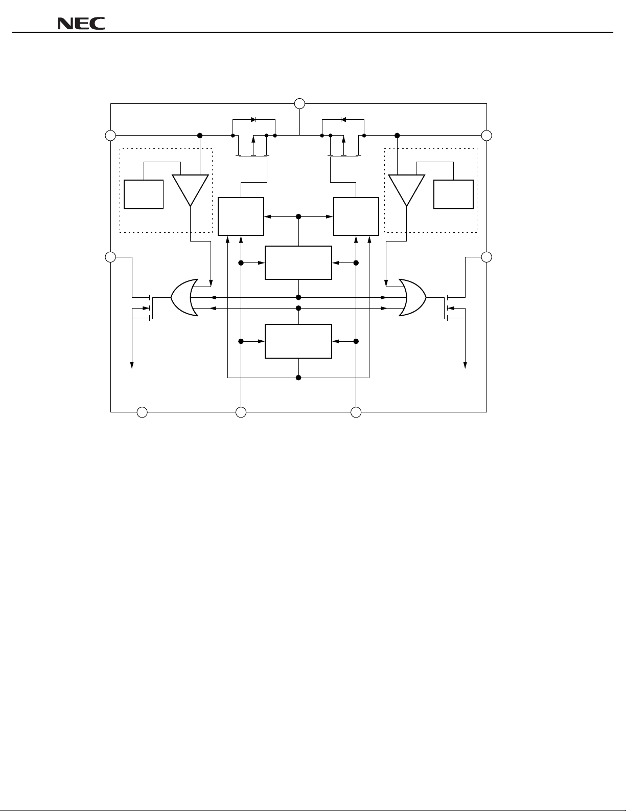
BLOCK DIAGRAM
IN (Input)
7
µµµµ
PD16855
OUT1
(Output1)
FLG1
(Flag Out1)
8
2
Ref.
Voltage
Over Current
Detect
6
GND
Gate
Control
1
CTL1
(Control Input1)
UVLO
Thermal
Shutdown
Gate
Control
4
CTL2
(Control Input2)
Ref.
Voltage
Over Current
Detect
5
OUT2
(Output2)
3
FLG2
(Flag Out2)
The internal resister doesn’t connect to input terminal of CTL1 (1 pin) and CTL2 (4 pin).
Note
Therefore the input level must be “H” or “L” even if these pins aren’t used.
2
Data Sheet S13020EJ1V0DS00
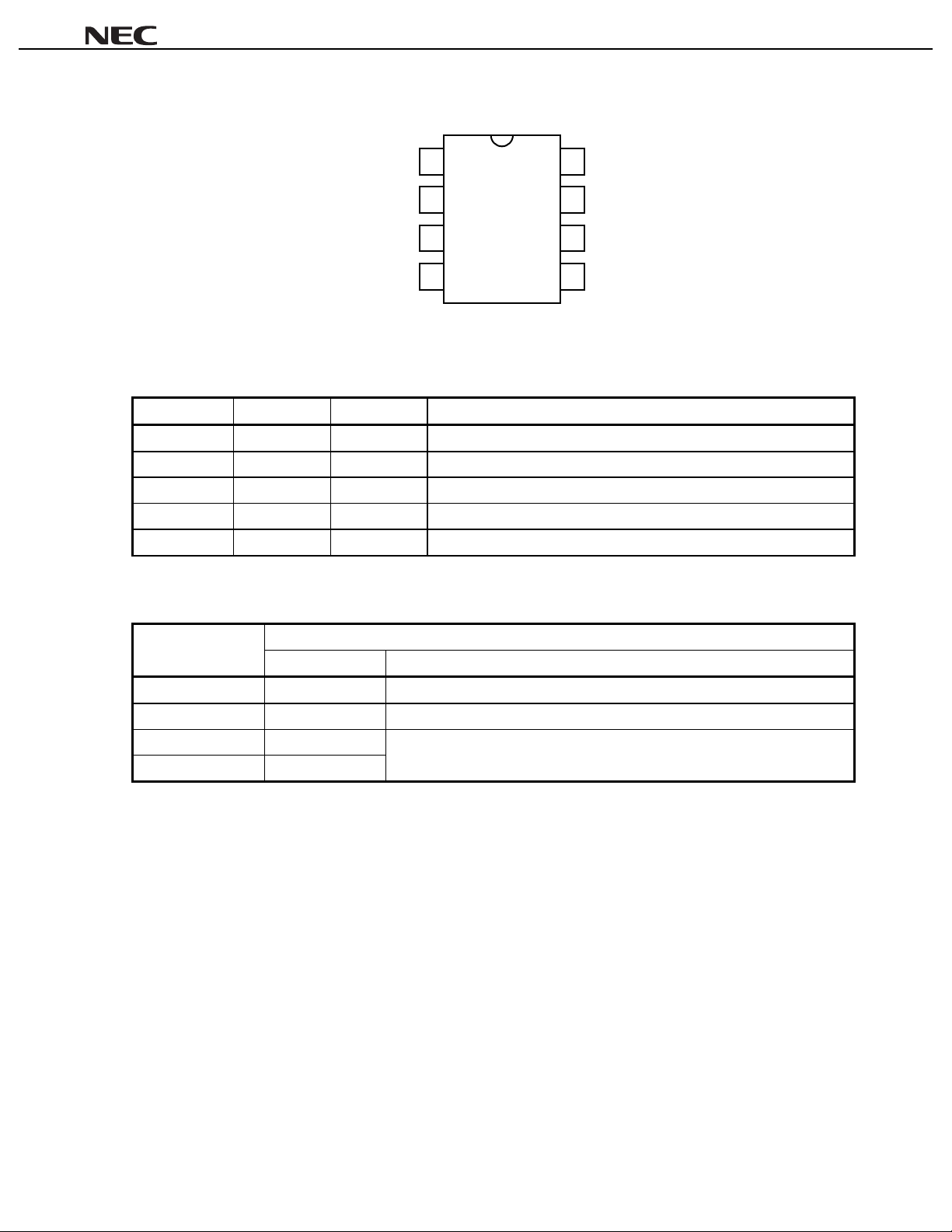
CONNECTION DIAGRAM (TOP VIEW)
1CTL1 OUT18
2FLG1 IN7
3FLG2 GND6
4CTL2 OUT25
8-Pin DIP/SOP
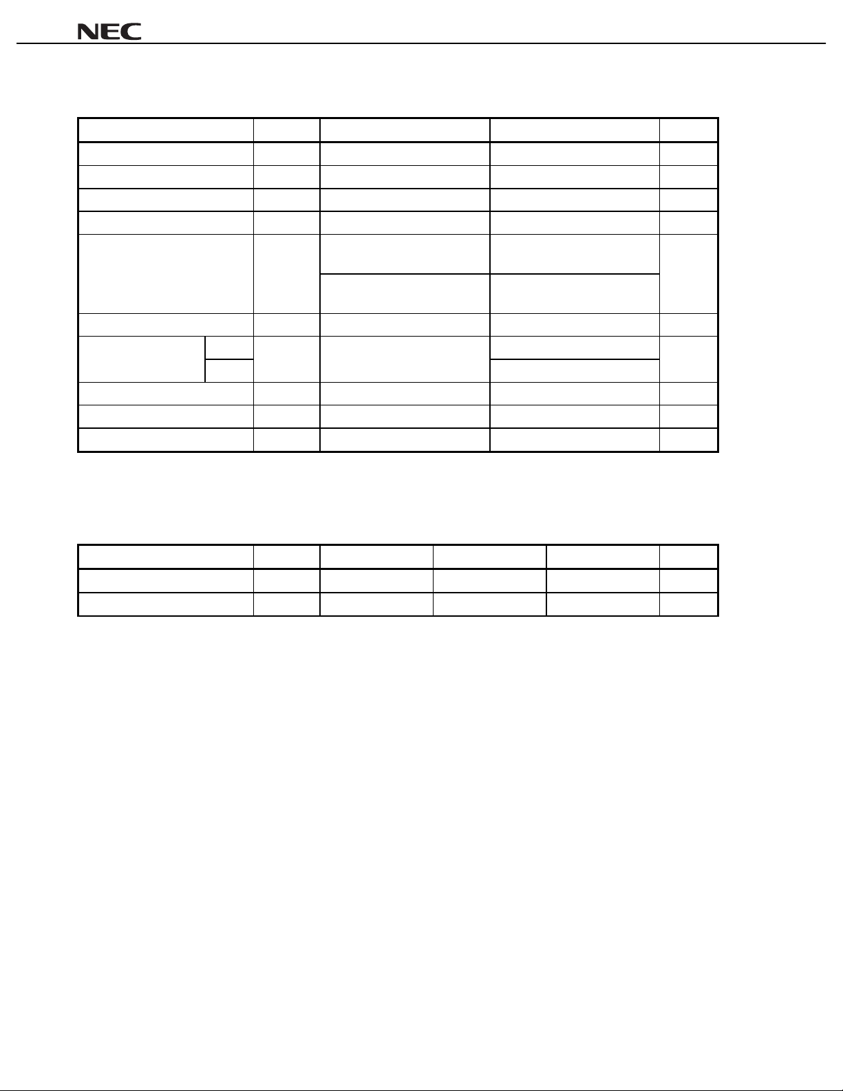
PIN CONFIGURATION
PIN No. SYMBOL I/O FUNCTION
1/4 CTL1/CTL2 Input Control : TTL Input
2/3 FLG1/FLG2 Output Over Current Detect Flag : Ac tive-L, Nch open-drain
6 GND Power G round
7 IN Power (Input) Power Supply : Source of MO S F ET
8/5 OUT1/OUT2 Output Output of Switch : Drain of MOSFET
µµµµ
PD16855
DESCRIPTION of
PART No.
PD16855AG “H” active Over-Current Limit Operation. Switch Off with CTL Input “L”
µ
PD16855BC/BG “L” active Over-Current Lim i t Operation. Switch Off wit h CTL Input “H”
µ
PD16855CG “H” active
µ
PD16855DG “L” active
µ
PD16855A/B/C/D FUNCTION
µµµµ
Abstract of Functi on
CTL Input Logic Switch Operation with Over-Current Detect
Switch Off regardless of CTL Input
Data Sheet S13020EJ1V0DS00
3
µµµµ
PD16855
PIN CONFIGURATION
PD16855AG (Active-H)
µµµµ
CTL1 FLG1 OUT1 CTL2 FLG2 OUT2 Operating mode
H H ON H H ON normal mode
H H ON L H OFF only OUT1 is ON
L H OFF H H ON only OUT2 is ON
L H OFF L H OFF st andby m ode
H L ON H H ON only OUT1 is over-current detect
H H ON H L ON only OUT2 is over-current detect
X L OFF X L OFF TSD mode
X L OFF X L OFF UVLO mode
PD16855BC/BG (Active-L)
µµµµ
CTL1 FLG1 OUT1 CTL2 FLG2 OUT2 Operating mode
L H ON L H ON normal mode
L H ON H H OFF only OUT1 is ON
H H OFF L H ON only OUT2 is ON
H H OFF H H OFF standby mode
L L ON L H ON only OUT1 is over-current detect
L H ON L L ON only OUT2 is over-current detect
X L OFF X L OFF TSD mode
X L OFF X L OFF UVLO mode
(H:Hi-level, L:Low-level, ON:output ON state, OFF:output OFF state, X:H or L)
4
Data Sheet S13020EJ1V0DS00
PD16855CG (Active-H and Switch off with over-current detect)
µµµµ
CTL1 FLG1 OUT1 CTL2 FLG2 OUT2 Operating mode
H H ON H H ON normal mode
H H ON L H OFF only OUT1 is ON
L H OFF H H ON only OUT2 is ON
L H OFF L H OFF st andby m ode
H L OFF H H ON only OUT1 is over-current detect
H H ON H L OFF only OUT2 is over-current detect
X L OFF X L OFF TSD mode
X L OFF X L OFF UVLO mode
PD16855DG (Active-L and Switch off with over-current detect)
µµµµ
CTL1 FLG1 OUT1 CTL2 FLG2 OUT2 Operating mode
L H ON L H ON normal mode
L H ON H H OFF only OUT1 is ON
H H OFF L H ON only OUT2 is ON
H H OFF H H OFF standby mode
L L OFF L H ON only OUT1 is over-current detect
L H ON L L OFF only OUT2 is over-current detect
X L OFF X L OFF TSD mode
X L OFF X L OFF UVLO mode
µµµµ
PD16855
Data Sheet S13020EJ1V0DS00
5
µµµµ
PD16855
ABSOLUTE MAXIMUM RATINGS (TA = 25
Parameter Symbol Conditions Ratings Unit
Input Voltage V
Flag Voltage V
Flag Current I
Output Voltage V
Output Current I
Control Input Voltage V
DIP 400Power Dissipation
SOP
Operating Temperature Range T
Channel Temperature Range T
Storage Temperature Range T
The thermal shutdown circuit (operating temperature is more than 150 °C typ.) builds in this product.
Note
IN
FLG
FLG
OUT
OUT
CTL
D
P
A
CH MAX
stg
C)
°°°°
DC +0.5(VIN = V
Pulse Width ≤ 100µs
Single Pulse
–0.3 to +6 V
–0.3 to +6 V
50 mA
VIN + 0.3 V
CTL
=5 V)
–0.1 (V
IN
= 0V, V
OUT
= 5V)
+3
–0.3 to +6 V
300
–40 to +85 °C
+150 °C
–55 to +150 °C
A
mW
RECOMMENDED OPERATING RANGE
Parameter Symbol Min Typ Max Unit
Input Voltage V
Operating Temperature Range T
IN
A
+4 +5.5 V
0+70°C
6
Data Sheet S13020EJ1V0DS00
ELECTRICAL CHARACTERISTICS
DC CHARACTERISTICS (Unless otherwise specified, V
Parameter Symbol Conditions Min Typ Max Unit
IN
= +5V; TA = +25°C)
µµµµ
PD16855
PD16855A/C)
(only
µ
PD16855B/D)
(only
µ
Low-level Input Voltage V
High-level Input Voltage V
Output Leak Current I
O LEAK
Over Current Detect Threshold I
Flag Output Resistance R
Flag Leak Current I
Operating Voltage of
O LEAK F
V
Under Voltage Locked Out
Circuit
DD
I
DD
I
IL
IH
CTL
ON
TH
ON F
UVLO
CTL
V
= 0V (both 1 pin & 4 pin),
15
µ
OUT = open
CTL
V
= VIN, OUT = open 1 1.5 mA
CTL
V
= VIN (both 1 pin & 4 pin),
15
µ
OUT = open
CTL
V
= 0V, OUT = open 1 1.5 mA
CTL Pin 1.0 V
CTL Pin 2.0 V
CTL
V
= 0V 0.01 1
CTL
IN
V
= V
TA = 0 to +70 °C,
OUT
= 500 mA
I
DIP 100 140Output MOSFET On Resis tance R
SOP 100 130
0.01 1
10
µ
µ
m
µ
TA = 0 to +70 °C 0.6 0.9 1.25 A
IL = 10 mA 10 25
FLAG
V
= 5 V 0.01 1
µ
VIN : Up 3.2 3.5 3.7 V
VIN : Down 3.0 3.3 3.5 V
Hysteresis 0.1 0.2 0.3 V
ACircuit Current
ACircuit Current
AInput Current of CTL pin I
A
Ω
A
Ω
A
AC CHARACTERISTICS (Unless otherwise specified, VIN = +5 V; TA = +25
Parameter Symbol Conditions Min Typ Max Unit
Output Transition
Rising Time
Output Transition
Falling Time
Over Current Detect
Delay Time
CTL Input Low-Level Time
PD16855A/C)
(only
µ
CTL Input High-Level Time
PD16855B/D)
(only
µ
RISE
t
FALL
t
OVER
t
t
t
CTL
CTL
RL = 10 Ω each output 2.5 12 ms
RL = 10 Ω each output 10
520
CTL : H→L→H20
CTL : L→H→L20
C)
°°°°
s
µ
s
µ
s
µ
s
µ
Data Sheet S13020EJ1V0DS00
7
MEASUREMENT POINT
Output Transition Rising Time (at ON)/Output Transition Falling Time (at OFF)
at the timing of CTL changing “L” to “H”/“H” to “L” for µPD16855A/C
5 V/3.3 V
µµµµ
PD16855
CTL
OUT
V
0 V
5 V
0 V
10%
t
RISE
90% 90%
at the timing of CTL changing “H” to “L”/“L” to “H” for µPD16855A/C
5 V/3.3 V
0 V
5 V
0 V
90%
t
RISE
90% 90%
CTL
OUT
V
t
FALL
t
FALL
10%
10%
8
Data Sheet S13020EJ1V0DS00
Over Current Detect Delay Time/CTL Input Low-Level Time for µPD16855A/C
µµµµ
PD16855
IOUT
VOUT
FLG
CTL
tOVER
µ
PD16855A
PD16855C
µ
90%
90% 90%
ITH
tCTL
Over Current Detect Delay Time/CTL Input High-Level Time for µPD16855B/D
I
OUT
ITH
V
OUT
FLG
CTL
t
OVER
PD16855B
µ
PD16855D
µ
90%
t
CTL
10% 10%
Data Sheet S13020EJ1V0DS00
9

µµµµ
PD16855
FUNCTION DESCRIPTION
1. Over current detection
The specification of over current detect is 0.6 to 1.25 A (typ. 900mA) in this IC. (500 mA max. in USB standard)
This function is that flag-pin turns to Low-level and reports to the USB controller when over current is detected.
At this time, output of IC is operated as followed.
PD16855A/B : Output keep ON-state and over current limited circuit is operated. This function can be
•
µ
prevented from being long-time over current state.
PD16855C/D : Output turns to off, and isn't based on the state of CTL-pin.
•
µ
When CTL-pin turns to non-active, FLG-pin returns to High-level and Output-pin turn to OFF-state.
Immediately the controller should be inputted non-active level to CTL-pin after detecting FLG = “L” not to reach to
the state of thermal shutdown.
Then, in the case of FLG-pin is High-level and CTL-pin is active level, Output-pin turns to ON-state.
To prevent from detecting wrongly the current to the moment, over current detect delay time is set up.
This delay time is 10 µs (typ.).
Power consumption in this device increases rapidly at the time of current-limitter circuit operation, and channel
temperature Tch is likely to escalate. Make a CTL signal non-active, and make switch turn off before Tch of this
device exceed absolute maximum rating.
Flg
Vout
Iout
Flg
Iout
0.5 A
5 V
0 V
0 A
5 V
0 V
1 A~
Normal Mode
more than 10 s (typ.)
in case of current surge
less then 10 s (typ.)
µ
Controlled by CTL-pin ( PD16855A/B)
Instant Switch off ( PD16855C/D)
Over current detect threshold
PD16855 USB Device
µ
IN
µ
µ
connection to the
moment, it flow
the large current
OUT
+
µ
10
Data Sheet S13020EJ1V0DS00

2. Under Voltage Locked Out (UVLO) Circuit
UVLO is the circuit for preventing malfunction of the switch by voltage variation.
In the Power Up : less than 3.5 V (typ.) and in the Power Down : less than 3.3 V (typ.)
OUT : OFF
FLG : “L” ( = 0V)
5 V
Output
3.3 V 3.5 V 5 V
Input
µµµµ
PD16855
3. Behavior in the case of Power ON
This IC is slowly started up by Soft-Start Operation when IC is powered on.
This function is to prevent from flowing large current in the period of charging the capacitor which is connected to
Output-pin.
In Power ON state, Soft-Start Time is 5ms (typ.)
5 V
Vin
0 V
µ
2.5 ms min.
12 ms max.
5 V
V
OUT
0 V
10 s
max.
Data Sheet S13020EJ1V0DS00
11

OPERATING SEQUENCE
Power On/Power Off
5 V
µµµµ
PD16855
IN (input)
OUT
(output)
Flg
(output)
PD16855A/C
µ
CTL
(input)
PD16855B/D
µ
Iout
If CTL-pin is active level after IC is powered on, This IC's Output is started Soft-Start Operation
Note
GND
5 V
GND
5 V
GND
5 V
GND
5 V
GND
over current detect threshold
(Output Transition Rising Time : 12ms max.).
When Power-voltage is less than UVLO operating voltage, FLG-pin is fixed on Low-Level.
If CTL1 and CTL2 pins are non-active level, this IC moves to Stand-by mode (I
DD
= 5 µA max.)
Input controlled-signal
IN (input)
OUT
(output)
Flg
(output)
µ
CTL
(input)
µ
5 V
GND
5 V
GND
5 V
GND
5 V
PD16855A/C
GND
5 V
PD16855B/D
GND
12
Data Sheet S13020EJ1V0DS00

Over current detect
PD16855A/B
µ
IN (input)
Flg
(output)
PD16855A
µ
CTL
(input)
PD16855B
µ
OUT
(output)
5 V
5 V
GND
5 V
GND
5 V
GND
GND
5 V
GND
µµµµ
PD16855
PD16855C/D
µ
Iout
IN (input)
Flg
(output)
PD16855C
µ
CTL
(input)
PD16855D
µ
OUT
(output)
Iout
over current detect threshold
over current detect
5 V
GND
5 V
GND
5 V
GND
5 V
GND
5 V
GND
over current detect threshold
over current detect
If Over current detect circuit is operated, FLG-pin is Low-Level and over current limit circuit is operated. At
Note
this time, output's operation is as followed.
PD16855A/B : output is OFF and Flg-pin is High-Level when CTL-pin is non-active level.
µ
PD16855C/D : output synchronizes in Flg-pin = “L”, and is OFF.
µ
Flg-pin is High-Level when CTL-pin is non-active level.
And then when CTL-pin turns to active level again, if UVLO and TSD are not operated, Output-pin is reset
to ON-state.
Data Sheet S13020EJ1V0DS00
13

Thermal shutdown
IN (input)
OUT
(output)
Flg
(output)
PD16855A/C
µ
CTL
(input)
PD16855B/D
µ
5 V
GND
5 V
GND
5 V
GND
5 V
GND
5 V
GND
not Stand-by
Stand-by
µµµµ
PD16855
Tch
In operating the thermal shutdown, the status of output-pin is OFF.
Note
Thermal shutdown
operating temperature (up)
Thermal shutdown
operating temperature (down)
In this case, however, if CTL-pin is kept non-active level, this IC isn’t in stand-by mode.
And, thermal shutdown circuit can not be operated in both CTL1-pin and CTL2-pin are non-active
level (equal to stand-by mode), if junction-temperature of this IC exceed 150 degree (typ.).
14
Data Sheet S13020EJ1V0DS00

µµµµ
PD16855
CHARACTERISTICS CURVES (unless otherwise specified, TA = 25
PT - TA Rating
500
400
(mW)
T
300
200
100
Total Power Dissipation P
0
RON - TA Characteristics
140
120
(Ω)
100
ON
80
60
40
On Resistance R
20
0
−20 0 20 40 60 80
Ambient Temperature T
DIP
SOP
−40 0 40 80 120 160 200
Note
A
(°C)
Ambient Temperature T
A
(°C)
RON - VIN Characteristics
140
120
(Ω)
100
ON
80
60
40
On Resistance R
20
0
3.5 4 4.5 5 5.5 6
Ambient Temperature V
C, VIN = 5 V) (Nominal)
°°°°
Note
IN
(V)
IDD - TA Characteristics
1.0
(mA)
0.8
DD
0.6
0.4
0.2
Current Consumption I
0.0
−20 0 20 40 60 80
A
Ambient Temperature T
I
DD STB
- TA Characteristics
0.10
µ
( A)
0.08
DD STB
0.06
0.04
0.02
Current Consumption I
0.00
−20 0 20 40 60 80
Ambient Temperature T
ON
–TA Characteristics and RON – VIN Characteristics show the characteristics for SOP Package.
R
Note
(°C)
A
(°C)
IDD - VIN Characteristics
1.0
(mA)
0.8
DD
0.6
0.4
0.2
Current Consumption I
0.0
3.5 4 4.5 5 5.5 6
IN
Power Supply V
I
DD STB
- VIN Characteristics
0.10
µ
( A)
0.08
DD STB
0.06
0.04
0.02
Current Consumption I
0.00
3.5 4 4.5 5 5.5 6
Power Supply V
(V)
IN
(V)
Data Sheet S13020EJ1V0DS00
15

µµµµ
PD16855
CHARACTERISTICS CURVES (unless otherwise specified, TA = 25
VIL - TA Characteristics
3.0
(V)
IL
2.5
2.0
1.5
1.0
0.5
Low Level Input Voltage V
0.0
−20 0 20 40 60 80
A
Ambient Temperature T
(°C)
VIH - TA Characteristics
3.0
(V)
2.5
IH
2.0
1.5
3.0
(V)
IL
2.5
2.0
1.5
1.0
0.5
Low Level Input Voltage V
0.0
3.5 4.0 4.5 5.0 5.5 6.0
3.0
(V)
2.5
IL
2.0
1.5
C, VIN = 5 V) (Nominal)
°°°°
VIL - VIN Characteristics
IN
Power Supply V
(V)
VIH - VIN Characteristics
1.0
0.5
High Level Input Voltage V
0.0
−20 0 20 40 60 80
A
Ambient Temperature T
(°C)
ITH - TA Characteristics
(A)
1.2
TH
1.1
1.0
0.9
0.8
0.7
0.6
Over Current Detect Curent I
−20 0 20 40 60 80
A
Ambient Temperature T
(°C)
1.0
0.5
Low Level Input Voltage V
0.0
3.5 4.0 4.5 5.0 5.5 6.0
IN
Power Supply V
(V)
ITH - VIN Characteristics
(A)
1.2
TH
1.1
1.0
0.9
0.8
0.7
0.6
Over Current Detect Curent I
3.5 4.0 4.5 5.0 5.5 6.0
IN
Power Supply V
(V)
16
Data Sheet S13020EJ1V0DS00

µµµµ
PD16855
CHARACTERISTICS CURVES (unless otherwise specified, TA = 25
Output Transition Rising Time
5
4
3
Voltage (V)
2
1
0
4.0
(V)
3.8
UVLO
3.6
Input Voltage
Output Voltage
21043
Time (ms)
UVLO circuit operating voltage Characteristics
UVLO(L→H)
5
4
3
Voltage (V)
2
1
0
C, VIN = 5 V) (Nominal)
°°°°
Output Transition Falling Time
Output Voltage
0.40 1.20.8
Time ( s)
µ
3.4
3.2
UVLO Operating Voltage V
3.0
−200 20406080
Ambient Temperature T
UVLO(H→L)
A
(°C)
Data Sheet S13020EJ1V0DS00
17

MEASUREMENT CIRCUIT
10 kΩ 10 kΩ
5 V
µµµµ
PD16855
CTL1 OUT1
FLG1 IN
FLG2 GND
CTL2 OUT2
PD16855
µ
1 F
µ
10 Ω
10 Ω
18
Data Sheet S13020EJ1V0DS00

APPLICATION CIRCUIT
Example 1
Over
Current
Enable
USB
Controller
Example 2
Enable
USB
Controller
Timing chart Example 2
D+
D−
D+
D−
Over
Current
5 V
10 kΩ
OUT1
CTL1
FLG1
FLG2
CTL2
PD16855A
µ
GND
OUT2
IN
1 F
µ
150 F
µ
USB OUTPUT Port : 1 port
µ
Use PD16855A
Not need to control by USB-controller (CTL-input is "H"-active)
5 V3.3 V
10 kΩ10 kΩ
CTL1
OUT1
FLG1
FLG2
CTL2
OUT2
PD16855B
µ
GND
IN
1 F
µ
150 F
µ
150 F
µ
USB
Connector
USB OUTPUT Port : 2 port
µ
Use PD16855B
controllable by USB-controller (CTL-input is "L"-active)
V
BUS
D+
D−
GND
BUS
V
D+
D−
GND
V
BUS
D+
D−
GND
µµµµ
PD16855
5 V
IN (input)
OUT
(output)
Flg
(output)
CTL
(input)
Iout
GND
5 V
GND
5 V
GND
5 V
GND
over current detect threshold
over current detect
The application circuits and their parameters are for references only and are not intended for use in actual designin's.
Data Sheet S13020EJ1V0DS00
19

APPLICATION CIRCUIT
Example 3
Over
Current
USB
Controller
Example 4
Controller
Timing chart Example 4
IN (input)
OUT
(output)
D+
D−
Over
Current
USB
10 kΩ
OUT1
CTL1
IN
FLG1
GND
FLG2
OUT2
CTL2
PD16855C
µ
USB OUTPUT Port : 1 port
µ
Use PD16855C
controllable by USB-controller
D+
D−
10 kΩ10 kΩ
CTL1
OUT1
FLG1
FLG2
CTL2
µ
USB OUTPUT Port : 2 port
µ
Use PD16855D
Not need to control by USB-controller
IN
GND
OUT2
PD16855D
5 V
GND
5 V
GND
5 V
1 F
µ
5 V3.3 V
1 F
µ
150 F
µ
150 F
µ
150 F
µ
V
D+
D−
GND
V
D+
D−
GND
USB
Connector
V
BUS
D+
D−
GND
BUS
BUS
µµµµ
PD16855
Flg
5 V
(output)
GND
5 V
CTL
(input)
Iout
GND
over current detect threshold
over current detect
The application circuits and their parameters are for references only and are not intended for use in actual designin's.
20
Data Sheet S13020EJ1V0DS00
PACKAGE DRAWING
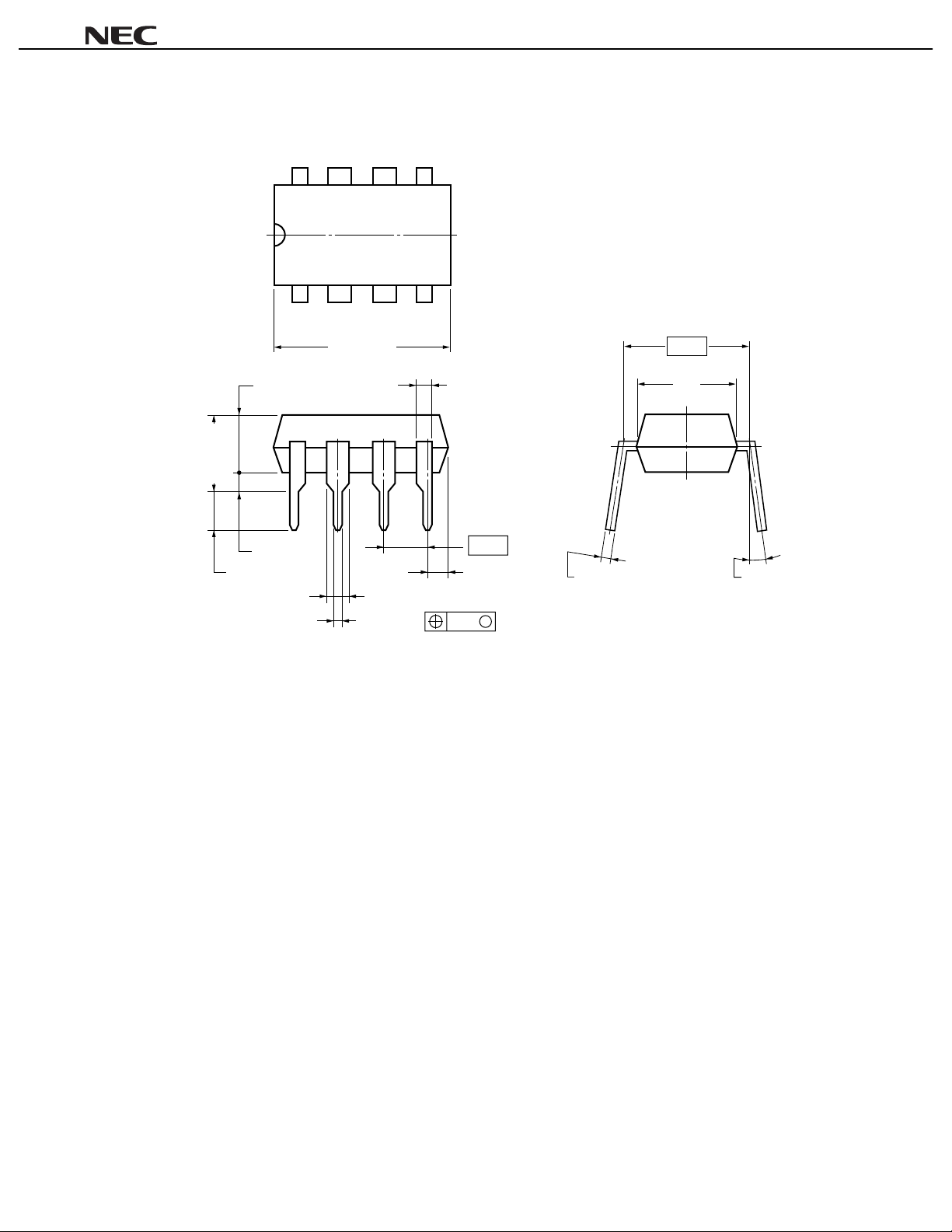
8 PIN PLASTIC DIP (300 mil)
85
µµµµ
PD16855
4.31 MAX.
5.08 MAX.
0.51 MIN.
3.2 ± 0.3
1
10.16 MAX.
1.4 MIN.
0.50 ± 0.10
4
0.9 MIN.
2.54
1.27 MAX.
M
0.25
+0.10
D0.05
7.62
6.4
0~15°0.25
Data Sheet S13020EJ1V0DS00
21

8 PIN PLASTIC SOP (225 mil)
85
µµµµ
PD16855
1.44
1.8 MAX
14
5.37 MAX.
0.78 MAX.
1.27
0.05 MIN.
0.40
+0.10
−0.05
0.12
M
+0.10
0.15
−0.05
0.5±0.2
6.0±0.3
4.4
0.8
0.10
22
Data Sheet S13020EJ1V0DS00

µµµµ
PD16855
RECOMMENDED SOLDERING CONDITIONS
Soldering the µPD16855 under the conditions listed in the table below is recommended.
For soldering methods and conditions other than those recommended, consult NEC.
Surface Mount Type
For the details of the recommended soldering conditions of the surface mount type, refer to information document
“Semiconductor Device Mounting Technology MANUAL” (C10535E)
PD16855AG,
µµµµ
Soldering process Soldering conditions Symbol
Infrared ray reflow Package peak temperature : 235 °C, Time : 30 seconds M A X.(210 °C MIN.),
VPS Package peak temperature : 215 °C , Time : 40 seconds M AX.(200 °C MIN.),
Wave soldering Soldering bath temperature : 260 °C MAX. , Tim e : 10 seconds MAX., Num ber
Partial heating
method
PD16855BG,
µµµµ
Number of times : 2 , Number of days : not limited*
Number of times : 2 , Number of days : not limited*
of times : 1 , Number of days : not limited*
Pin temperature : 300 °C MAX. (lead temperature), Time : 3 sec onds MAX. (per
lead pin), Number of days : not l i m i ted*
PD16855CG,
µµµµ
PD16855DG
µµµµ
IR35-00-2
VP15-00-2
WS60-00-1
* The number of days the devices can be stored at 25 °C, 65 % RH MAX. after the dry pack has been opened.
Caution Do not use two or more soldering methods in condition(except the pin partial heating method).
Throught-hole Type
PD16855BC
µµµµ
Soldering process Soldering conditions Symbol
Wave soldering Soldering bath temperature : 260 °C MAX., Tim e : 10 seconds MAX.
REFERENCE
Document Name Document No.
NEC semiconductor device reliability/quality control system IEI-1212
Quality grade on NEC semiconductor devices C11531E
Semiconductor device mounting technology manual C10535E
NEC IC Package Manual (CD-ROM) C13388E
Guide to quality assurance for semiconductor devices MEI-1202
Semiconductor selection guide X10679E
Data Sheet S13020EJ1V0DS00
23

NOTES FOR CMOS DEVICES
1 PRECAUTION AGAINST ESD FOR SEMICONDUCTORS
Note: Strong electric field, when exposed to a MOS device, can cause destruction
of the gate oxide and ultimately degrade the device operation. Steps must
be taken to stop generation of static electricity as much as possible, and
quickly dissipate it once, when it has occurred. Environmental control must
be adequate. When it is dry, humidifier should be used. It is recommended
to avoid using insulators that easily build static electricity. Semiconductor
devices must be stored and transported in an anti-static container, static
shielding bag or conductive material. All test and measurement tools
including work bench and floor should be grounded. The operator should
be grounded using wrist strap. Semiconductor devices must not be touched
with bare hands. Similar precautions need to be taken for PW boards with
semiconductor devices on it.
µµµµ
PD16855
2 HANDLING OF UNUSED INPUT PINS FOR CMOS
Note: No connection for CMOS device inputs can be cause of malfunction. If no
connection is provided to the input pins, it is possible that an internal input
level may be generated due to noise, etc., hence causing malfunction. CMOS
device behave differently than Bipolar or NMOS devices. Input levels of
CMOS devices must be fixed high or low by using a pull-up or pull-down
circuitry. Each unused pin should be connected to V
resistor, if it is considered to have a possibility of being an output pin. All
handling related to the unused pins must be judged device by device and
related specifications governing the devices.
DD
or GND with a
3 STATUS BEFORE INITIALIZATION OF MOS DEVICES
Note: Power-on does not necessarily define initial status of MOS device. Produc-
tion process of MOS does not define the initial operation status of the device.
Immediately after the power source is turned ON, the devices with reset
function have not yet been initialized. Hence, power-on does not guarantee
out-pin levels, I/O settings or contents of registers. Device is not initialized
until the reset signal is received. Reset operation must be executed immediately after power-on for devices having reset function.
24
Data Sheet S13020EJ1V0DS00

[MEMO]
µµµµ
PD16855
Data Sheet S13020EJ1V0DS00
25

[MEMO]
µµµµ
PD16855
26
Data Sheet S13020EJ1V0DS00

[MEMO]
µµµµ
PD16855
Data Sheet S13020EJ1V0DS00
27

µµµµ
PD16855
• The information in this document is subject to change without notice. Before using this document, please
confirm that this is the latest version.
• No part of this document may be copied or reproduced in any form or by any means without the prior written
consent of NEC Corporation. NEC Corporation assumes no responsibility for any errors which may appear in
this document.
• NEC Corporation does not assume any liability for infringement of patents, copyrights or other intellectual property
rights of third parties by or arising from use of a device described herein or any other liability arising from use
of such device. No license, either express, implied or otherwise, is granted under any patents, copyrights or other
intellectual property rights of NEC Corporation or others.
• Descriptions of circuits, software, and other related information in this document are provided for illustrative
purposes in semiconductor product operation and application examples. The incorporation of these circuits,
software, and information in the design of the customer's equipment shall be done under the full responsibility
of the customer. NEC Corporation assumes no responsibility for any losses incurred by the customer or third
parties arising from the use of these circuits, software, and information.
• While NEC Corporation has been making continuous effort to enhance the reliability of its semiconductor devices,
the possibility of defects cannot be eliminated entirely. To minimize risks of damage or injury to persons or
property arising from a defect in an NEC semiconductor device, customers must incorporate sufficient safety
measures in its design, such as redundancy, fire-containment, and anti-failure features.
• NEC devices are classified into the following three quality grades:
"Standard", "Special", and "Specific". The Specific quality grade applies only to devices developed based on a
customer designated "quality assurance program" for a specific application. The recommended applications of
a device depend on its quality grade, as indicated below. Customers must check the quality grade of each device
before using it in a particular application.
Standard: Computers, office equipment, communications equipment, test and measurement equipment,
audio and visual equipment, home electronic appliances, machine tools, personal electronic
equipment and industrial robots
Special: Transportation equipment (automobiles, trains, ships, etc.), traffic control systems, anti-disaster
systems, anti-crime systems, safety equipment and medical equipment (not specifically designed
for life support)
Specific: Aircraft, aerospace equipment, submersible repeaters, nuclear reactor control systems, life
support systems or medical equipment for life support, etc.
The quality grade of NEC devices is "Standard" unless otherwise specified in NEC's Data Sheets or Data Books.
If customers intend to use NEC devices for applications other than those specified for Standard quality grade,
they should contact an NEC sales representative in advance.
M7 98. 8
 Loading...