

µ
µ µ
µ
查询UPD16647供应商
DATA SHEET
MOS INTEGRATED CIRCUIT
PD16647
402/384-OUTPUT TFT-LCD SOURCE DRIVER (64 GRAY SCALE)
DESCRIPTION
The µ PD16647 is a source driver for TFT-LCD 64 gray scale displays. Its logic circuit operates at 3.3 V and the
driver circuit operates at 5.0 V. The input data is digital data at 6 bits x 3 dots, and 260,000 colors can be displayed
in 64-value outputs γ -corrected by the internal D/A converter and 10 external power supplies. The clock frequency is
50 MHz MIN. µ PD16647 can be used in TFT-LCD panels conforming to the SVGA standards.
FEATURES
CMOS level input
•
402/384 outputs
•
6 bits (gray scale data) x 3 dots input
•
64-value output by 10 external power supplies and internal D/A converter
•
Output dynamic range : V
•
High-speed data transfer: f
•
Level of γ -corrected power supply can be inverted
•
Input data inversion function (INV)
•
Precharge-less output buffer
•
Logic supply voltage (V
•
Driver supply voltage (V
•
Slim TCP
•
SS2
+ 0.1 V to V
MAX
=50 MHz MIN.(internal data transfer rate at supply voltage V
DD1
) : 3.3 V ± 0.3 V
DD2
) : 5.0 V ± 0.5 V
DD2
−
0.1 V
DD1
of logic circuit =3.0 V)
ORDERING INFORMATION
Part Number Package
PD16647N-xxx TCP (TAB package)
µ
Remark
Document No. S13607EJ2V0DS00 (2nd edition)
Date Published August 1999 NS CP (K)
Printed in Japan
The TCP package is a custom-ordered item. Users are requested to consult with an NEC sales
representative.
The information in this document is subject to change without notice. Before using this document, please
confirm that this is the latest version.
Not all devices/types available in every country. Please check with local NEC representative for
availability and additional information.
The mark
••••
shows major revised points.
©
1998
1. BLOCK DIAGRAM
µ
µ
PD16647
µ µ
STHR
D
00 - D05
D
10 - D15
D
20 - D25
V
R,/L
CLK
Osel
INV
STB
Bcont
0
- V
STHL
V
DD1
134-bit bidirectical shift register
1C2
C
C
133
C
134
(3.3 V)
SS1
V
Data register
Latch
V
DD2
9
D/A converter
(5.0 V)
V
SS2
Remark
Output buffer
S1S2S
3
/xxx indicates active lo w signal.
S
402/384
2
Data Sheet S13607EJ2V0DS00
µ
µ
PD16647
µ µ
2. PIN CONFIGURATION (
B
cont
V
SS2
V
DD2
V
DD1
R,/L
INV
STHL
D
20
D
21
D
22
D
23
D
24
D
25
D
10
D
11
D
12
D
13
D
14
D
15
V
9
V
8
V
7
V
6
V
5
V
4
V
3
V
2
V
1
V
0
CLK S
STB S
D
00
D
01
D
02
D
03
D
04
D
05
STHR
V
SS1
V
DD2
V
SS2
O
sel
PD16647N-xxx)
µ
µ
µ µ
Copper foil
surface
S
402/384
S
401/383
S
400/382
S
399/381
S
212/194
S
211/193
S
S
S
S
S
S
S
S
S
S
S
S
S
S
S
S
210
209
208
207
206
205
204
203
202
201
200
199
198
197
196
195
194
193
S
4
S
3
S
2
S
1
Remark
This figure does not specify the TCP package.
Data Sheet S13607EJ2V0DS00
3
µ
µ
PD16647
µ µ
3. PIN DESCRIPTION
Pin Symbol Pin Name Description
402/384
S1 to S
D00 to D
D10 to D
D20 to D
R,/L Shift direction sel ect input This pin inputs/outputs start pulses in cascade mode.
STHR Right shift start pul se I/O R,/L = H : Inputs start pulse
STHL Left shift start pulse I/O R/L = H : Outputs start pulse
Bcont Bias control This pin can be used to finely control the bias current inside the output
CLK Shift clock input Inputs shift cl ock to shift regist er. Display data is loaded to data register at
STB Latch input Contents of data register are latched at rising edge, transferred to D/A
Osel Selection of number of out puts Selects number of outputs. This pin is int ernal l y pul l ed up t o V
9
V0 to V
INV Data inversion input Input data can be inverted when display data is loaded.
DD1
V
DD2
V
SS1
V
SS2
V
Driver output Output 64 gray-scale analog voltages converted from digital s i gnal s .
1
192
to S
, S
211/193
402/384
to S
)
402/384
Osel = H or open: 402 outputs (S
Osel = L : 384 outputs (S
193
S
05
Display data input Inputs 18-bit-wide display gray scal e data (6 bits) x 3 dots (RGB).
15
25
DX0 : LSB, DX5 : MSB
210
to S
outputs are invalid in 384 outputs .
1
to S
Shift direction of shift register is as follows:
1
402
S
→
→
402
, STHL output
1
, STHR output
S
R,/L = H : STHR input, S
R,/L = L : STHL input, S
R,/L = L : Outputs start pulse
R/L = L : Inputs start pul se
amplifier. In cas es when fine-control is neces sary, connect this pin t o V
using a resistor of 10 to 100kΩ (per IC). When this fine-control function is
not required, short-circuit this pin to V
Function/Bcont
.
DD2
. Refer to 7.
rising edge of this pin. S tart pulse output goes high at ris ing edge of 134th
clock after start pulse has been input, and serves as start pulse to driver in
next stage. 134th clock of dri ver in firs t stage s erves as s tart puls e of dri ver
in next stage.
converter, and output as analog voltage corresponding to display data.
Contents of internal shift register are c leared af ter S TB has been input . One
pulse of this signal is input when
PD16647 is started, and then device
µ
operates normally.
For STB input timi ng, refer to
Osel = H or open : 402 outputs (S
Osel = L : 384 outputs (S
-corrected power supply Inputs γ-corrected power from external source.
γ
SS2
V
≤ V9 ≤ V8 ≤ V7 ≤ V6 ≤ V5 ≤ V4 ≤ V3 ≤ V2 ≤ V1 ≤ V0 ≤ V
SS2
V
≤ V0 ≤ V1 ≤ V2 ≤ V3 ≤ V4 ≤ V5 ≤ V6 ≤ V7 ≤ V8 ≤ V9 ≤ V
9. Switching Characteristics Waveform.
1
402/384
1
to S
192
, S
to S
211/193
to S
)
402/384
Maintain gray scale power supply during gray scale voltage output.
INV = H : Inverts and loads input data.
INV = L : Does not invert input data.
Logic circuit power supply 3.3 V ± 0.3 V
Driver circuit power supply 5.0 V ± 0.5 V
Logic ground Ground
Driver ground Ground
)
Bias Current Control
DD1
.
)
DD2
or
DD2
DD2
Caution Be sure to turn on power in the order V
turn off power in the reverse order, to prevent the
sure to observe this power sequence even during a transition period.
4
Data Sheet S13607EJ2V0DS00
DD1
, logic input, V
DD2
, and gray scale power (V0 to V9), and
PD16647 from being damaged by latchup. Be
µ
µ
µ µ
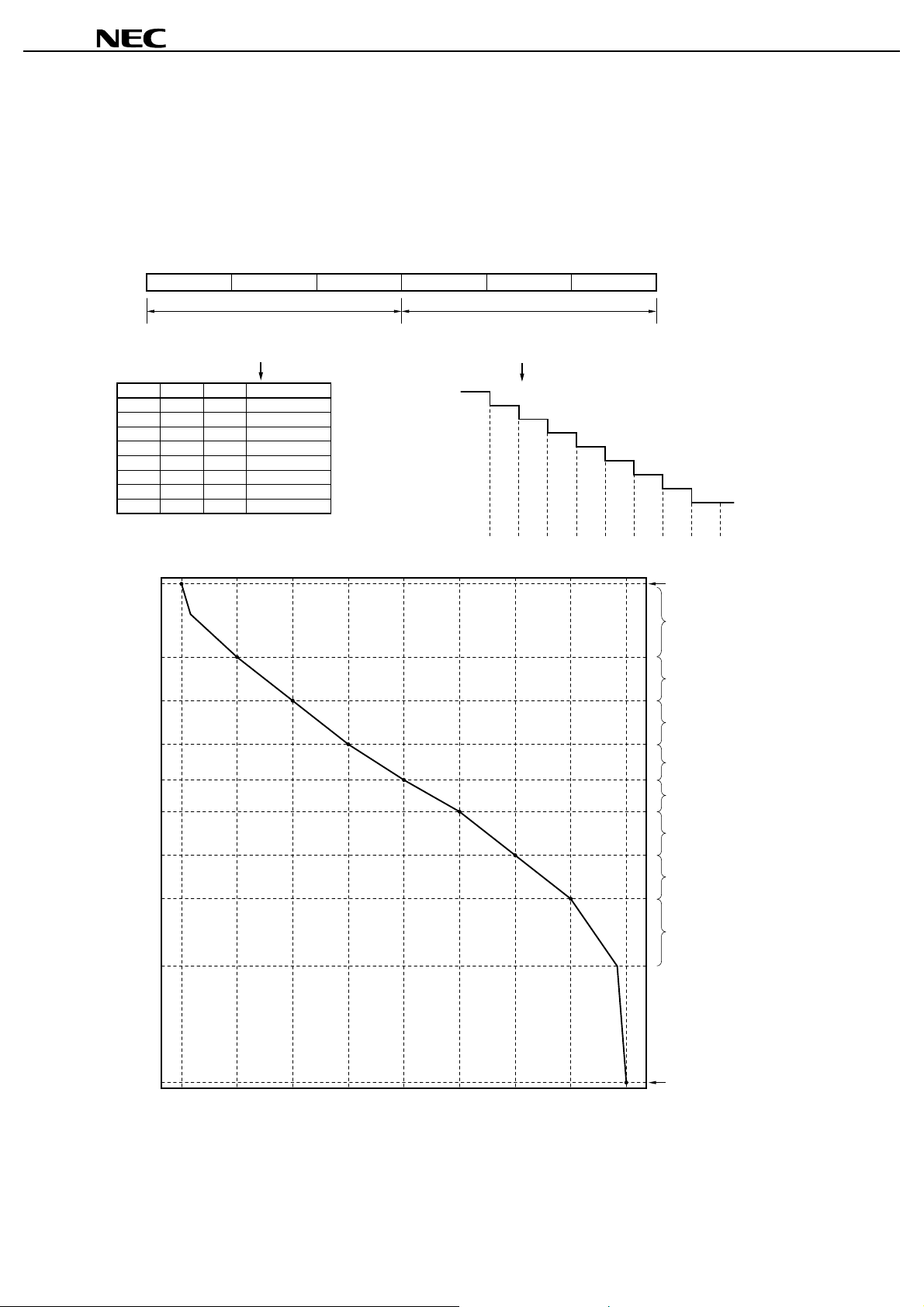
4. RELATION BETWEEN INPUT DATA AND OUTPUT VOLTAGE VALUE
µ
µ
PD16647
µ µ
The 10 major points on the γ -characteristic curve of the LCD panel are arbitrarily set by external power supplies V
through V9. If the display data is 00H or 3FH, gray scale voltage V0 or V9 is output. If the display data is in the range
n+1
01H to 3EH, the high-order 3 bits select an external power pair V
n+1
to Vn into eight segments by means of D/A conversion (however, the ranges from V8 to V7 and from V1 to V
of V
, Vn. The low-order 3 bits evenly divide the range
0
are divided into seven segments) to output a 64 gray scale voltage.
DX5(MSB) D
High-order 3 bits
: γ-corrected power selected
n
, V
(V
D
X5
D
X4
000
001
010
011
100
101
110
111
D
X4
D
X3
D
X2
D
X1
D
X0
(LSB)
Low-order 3 bits
n+1
: 3-bit D/A (range V
)
X3
V
n+1-Vn
V
1-V2
V
2-V3
V
3-V4
V
4-V5
V
5-V6
V
6-V7
V
7-V8
V
8-V9
V
n
n
to V
n+1
is divided to 7 or 8 segments)
8
V
n+1
0001001201030114100510161107111
Figure4-1. Relationship between Input Data and
V
0
V
DD2
γ-corrected Voltage
gray scale supply specified
by 00H
7 segments
0
V
1
8 segments
V
2
8 segments
V
3
8 segments
V
4
8 segments
V
5
8 segments
V
6
8 segments
V
7
7 segments
V
8
V
9
V
SS2
07F171F
27 2F 37 3F
gray scale supply specified
by 3FH
Input data (HEX)
Data Sheet S13607EJ2V0DS00
5
 Loading...