

Page 1

SERVICE MANUAL
SERVICE MANUAL
T571C
T571AH
DVD VIDEO PLAYER
T571C
T571AH
DVD VIDEO PLAYER
T571C
T571AH
DVD VIDEO PLAYER
MODELS : T571C/T571AHSERVICE MANUAL
© NAD 2001
NAD ELECTRONICS INTERNATIONAL
TORONTO
Page 2
NOTES) Warning
NOTES) Parts that are shaded are critical
NOTES) With respect to risk of fire or
NOTES) electricial shock.
470µF/2.3V
'01. 09. 21 R10581B
T571C/T571AH
3-17 3-18
CIRCUIT DIAGRAM
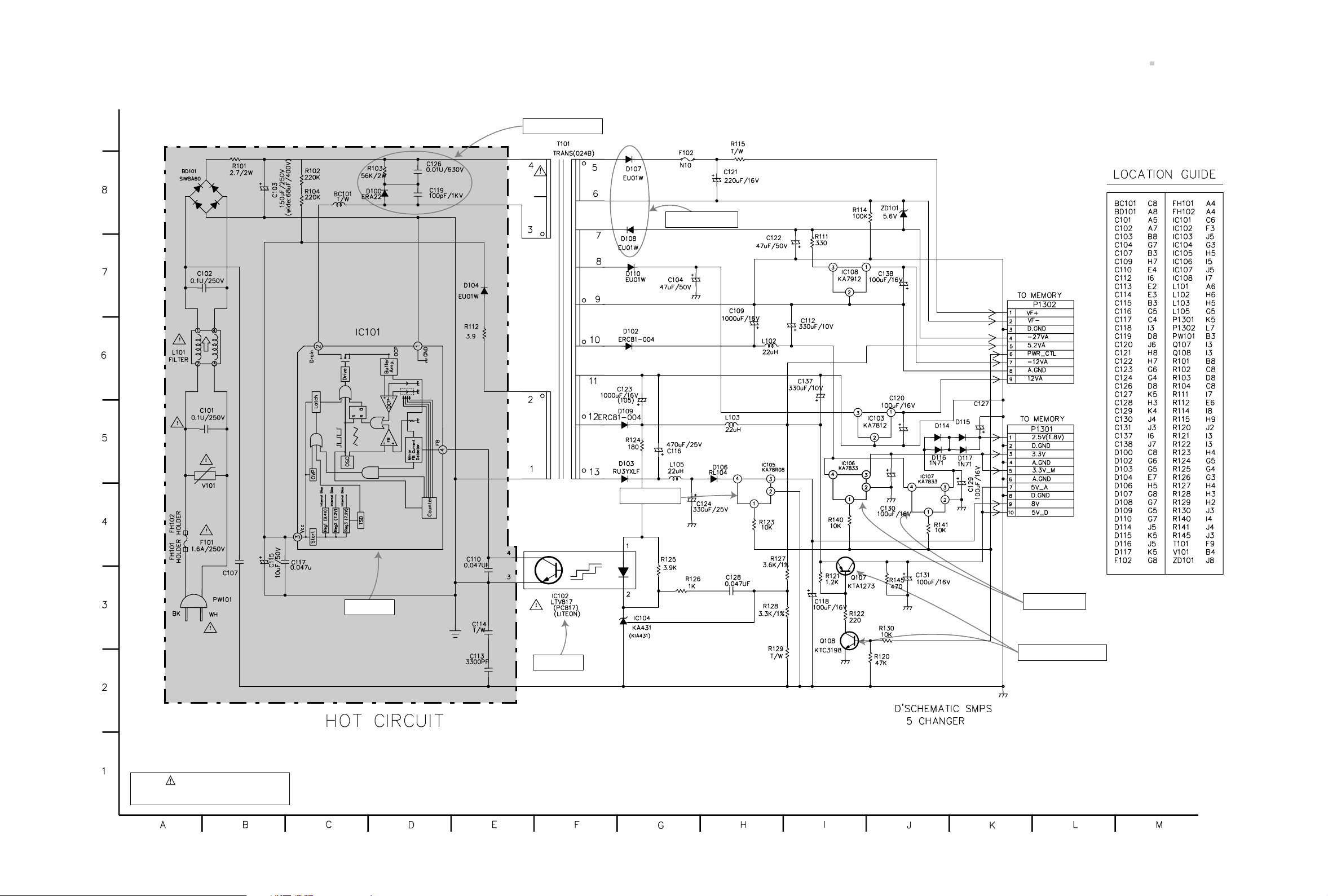
1. POWER(SMPS) CIRCUIT DIAGRAM
NOTE :
1. Shaded( ) parts are critical for safety. Replace only
with specified part number.
2. Voltages are DC-measured with a digital voltmeter
during Play mode.
Oscillation abnormal
Digitron no Power
3.3V line dead.
No Power
8V line dead
5V_A/5V_D, No Power
No Power
Page 3
3-19 3-20
5
56
Spindle Servo Loop
RF SIGNAL
Focus Servo Loop
Tracking Servo Loop
Sled Servo Loop
WAVEFORM
T571C/T571AH
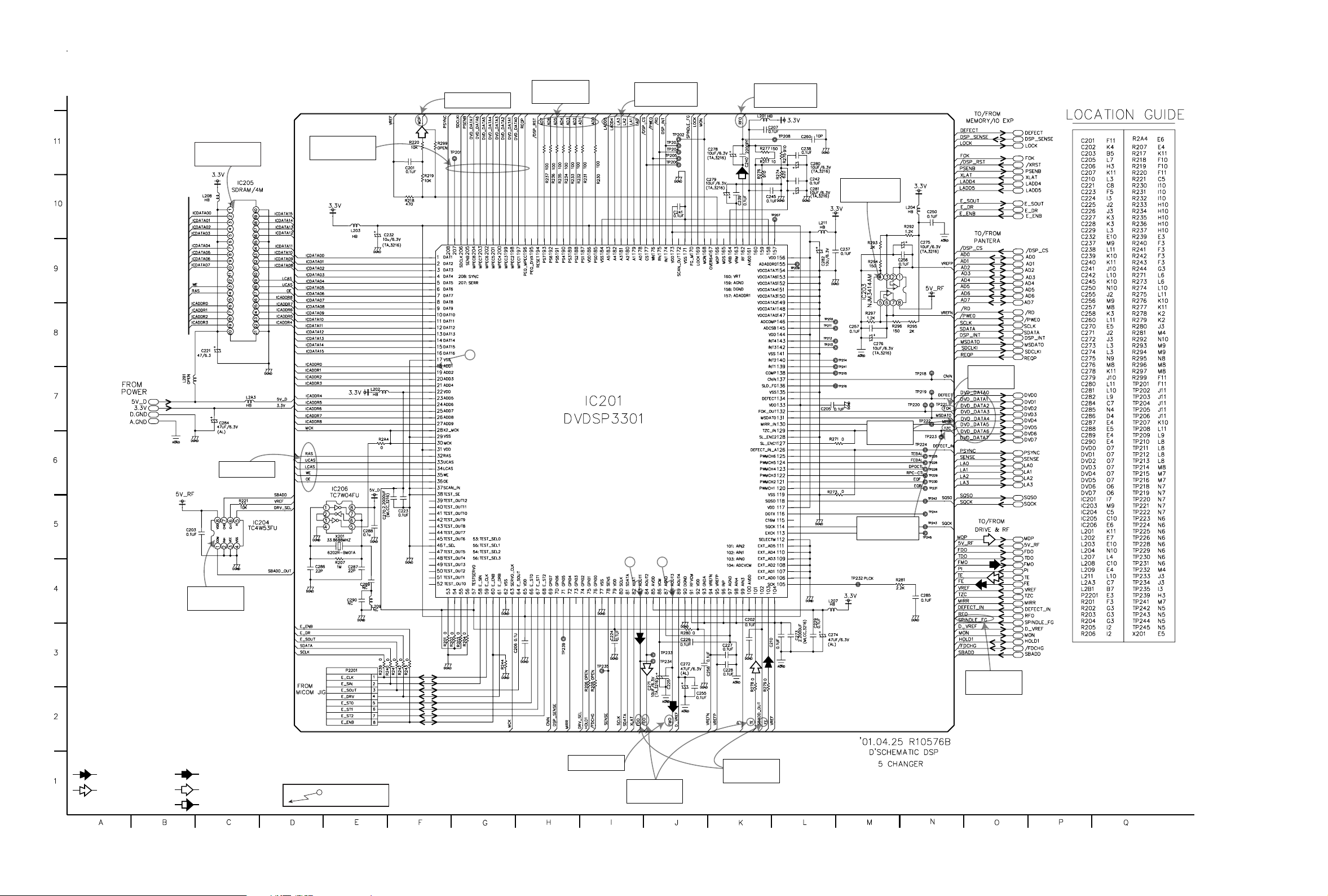
2. DVD DSP CIRCUIT DIAGRAM
DVD/CD picture
audio abnormal
MPEG Interface
Line
µ-com
Interface Data
µ-com
Interface adress
CD/DVD picture
audio abnormal
Tracking/Focus
Servo fail
Tracking
Servo fail
Spindle Motor
abnormal
CD/DVD picture
audio abnormal
Focus Servo
fail
Tracking
Servo fail
Scratched
Disc abnormal
Sled Servo fail
DRAM Control
Disc Detect
Error
Spindle Servo fail
Page 4
3-21 3-22
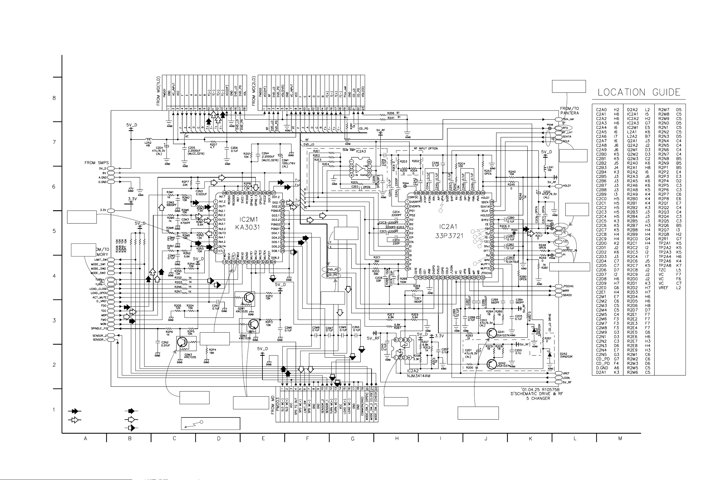
3. DRIVE & RF CIRCUIT DIAGRAM
4
1
6
2
3
1
WAVEFORM
Spindle Servo Loop
Turn Table Loop
Focus Servo Loop
Tracking Servo Loop
Sled Servo Loop
T571C/T571AH
Turntable
not operate
Tray Loading
Speed control
Turn table
speed control
Spindle Motor
unstable
Actuator spindle
sled not operate
DVD laser
not operate
CD laser
not operate
Servo fail
DVD Mode fail DVD
Laser not operate
Tracking Servo fail
Focus
Servo fail
µ-com
Interface line
CD/DVD picture
abnormal
Page 5
4
4
3
7
5
2 6
WAVEFORM
OPTICAL/COAXITAL OUT
Y/Pb/Pr(Component)
Y.c(S-VHS)
Audio L/R OUT
CVBS
T571C/T571AH
3-23 3-24
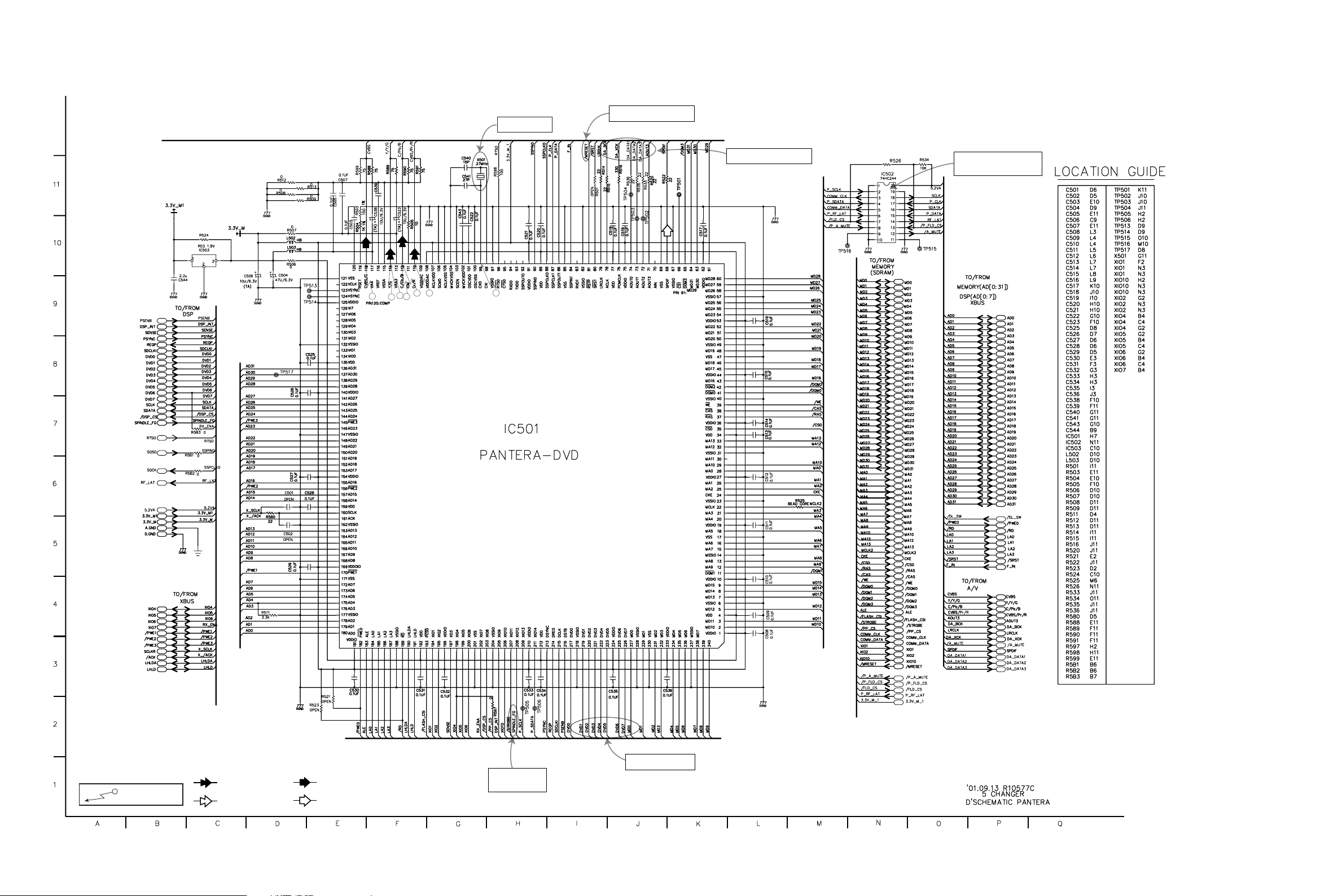
4. PANTERA CIRCUIT DIAGRAM
No Power on
Audio DAC Interface
System not operate
DSP interface line
Spindle Motor
unstable
System not working or
Digitron not display.
Page 6
3-25 3-26
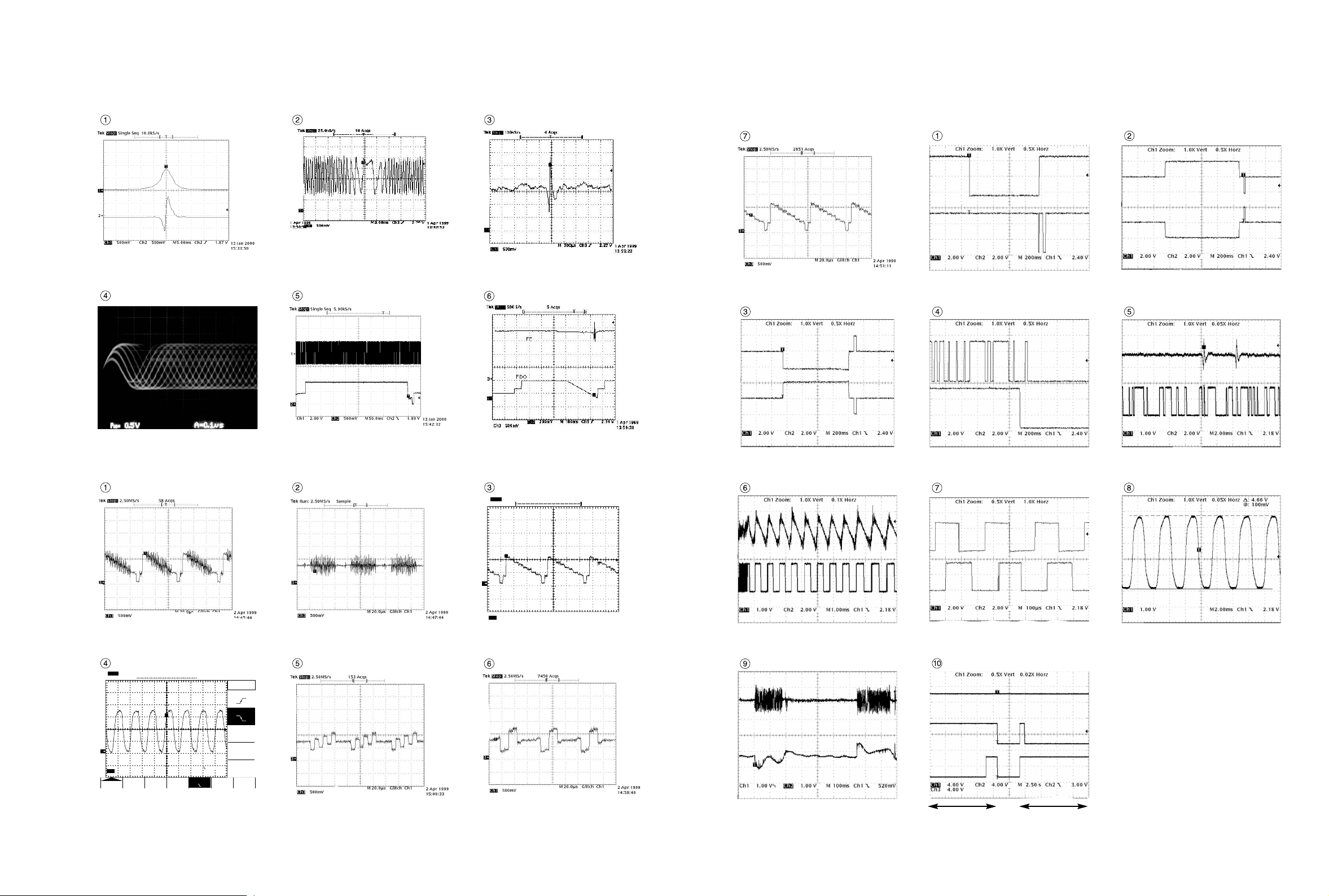
• WAVEFORMS
IC2A1 Pin 42, Focus Error
IC2A1 Pin 36, Pi
IC2A1 Pin 41
Tracking Error
IC501 Pin 114
Component Y
IC2A1 Pin 41
VBR TRACKING Error
IC2A1 Pin 57,
RF
IC201 Pin 88, SLED Drive(FMO)
IC201 Pin 18, SLED FG
IC2A1 Pin42, Focus Error(in Focus Search)
IC201 Pin 83, Focus Drive(FDO)
IC501 Pin 118, Composite IC501 Pin 112, Chrominance
(Super video out Mode)
Tek
Stop :
2.50MS/s
4 Acqs
M20.0µs
2 Apr 1999
14:47:27
Glitch
Ch1
Ch3
500mV
[T ]
T
3
IC501 Pin 114, Luminance
(Super video out Mode)
Tek
Stop :
1 00kS/s
3290 Acqs
M 500µs
CH1
280/mV
Edge Slope
Type
<Edge>
Source
Ch1
Coupling
DC
Level
280mV
Mode
&
Holdoff
3
Ch3
1.00V
[ T ][ T ]
Slope
T
IC501 Pin 99,
PANTER MAIN
IC501 Pin 112
Component Pb
IC501 Pin 110
Component Pr
TURN(+)(-) from Motor Drive
Reverse turn
Sensor 1 (disc position)
Sensor 2 (disc ready)
TURN(+)(-) Signal from µ-com
TE/TZC After tracking
servo ON (Play mode)
TURN(+)(-) from Motor Drive
Forward turn
TE/TZC Before tracking
servo ON
TZC/MIRR (Search mode) FG Signal from M/D
(Play mode)
TE/SLD(+) Search mode
(outter & inner) Tray open Tray closed
Page 7
3-27 3-28
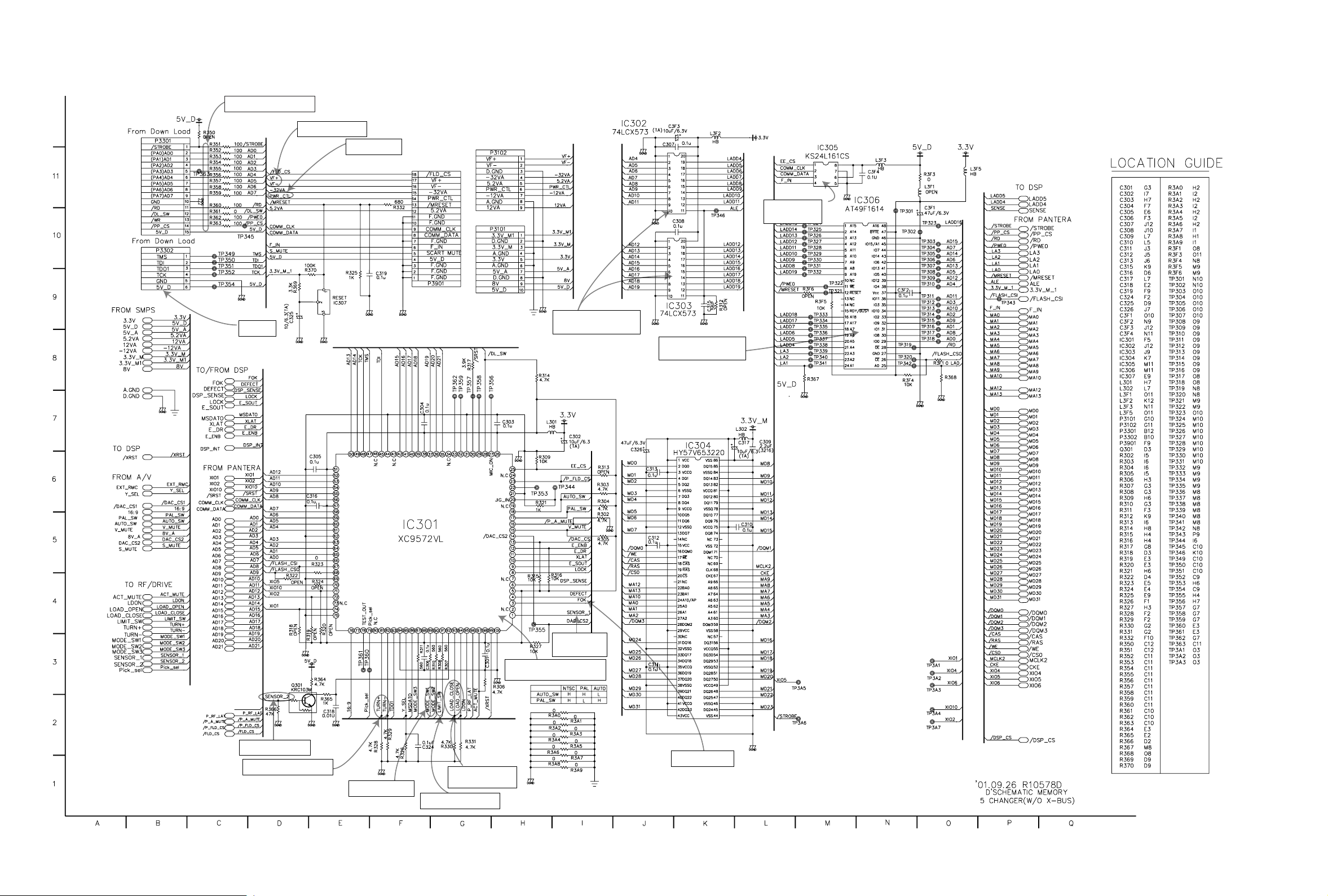
5. MEMORY CIRCUIT DIAGRAM
T571C/T571AH
Program download fail
Digitron abnormal
Not used
Not power on
Not memoried
setup Menu
Turntable not operating
“No Disc” display
Tray not open/close
Tray not closed
Pick-up not initial
operating
Disc Detec Error
Disc number
detect error
Digitron all not display and
system not operate
Digitron all not display
System not working
Digitron all not display
System not working
Page 8
3-29 3-30
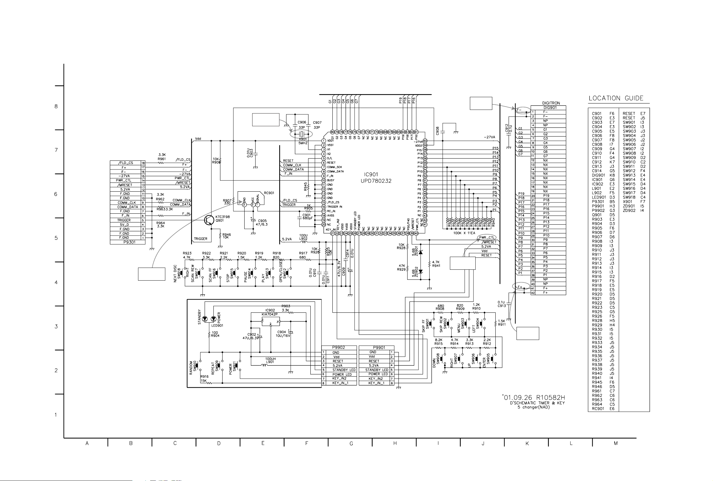
6. TIMER & KEY CIRCUIT DIAGRAM
T571C/T571AH
System not
operate
Remocon
not operate
Power not
control
Digitron
abnormal
Digitron
abnormal
Page 9
3-31 3-32
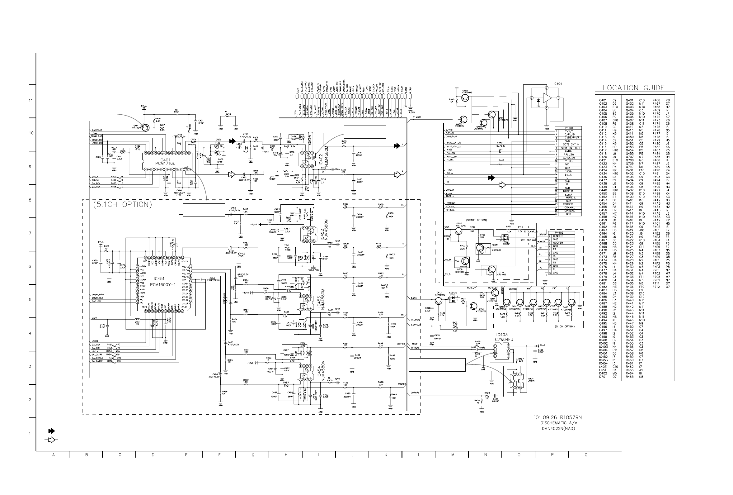
7. A/V CIRCUIT DIAGRAM
L
R
T571C/T571AH
Q401 is defective 2CH.
Audio out bad.
IC401 is defective.
2CH Audio out bad.
IC401 is defective.
2CH Audio out bad.
IC403, Q404 are defective.
Digital data out bad.
Page 10
3-33 3-34
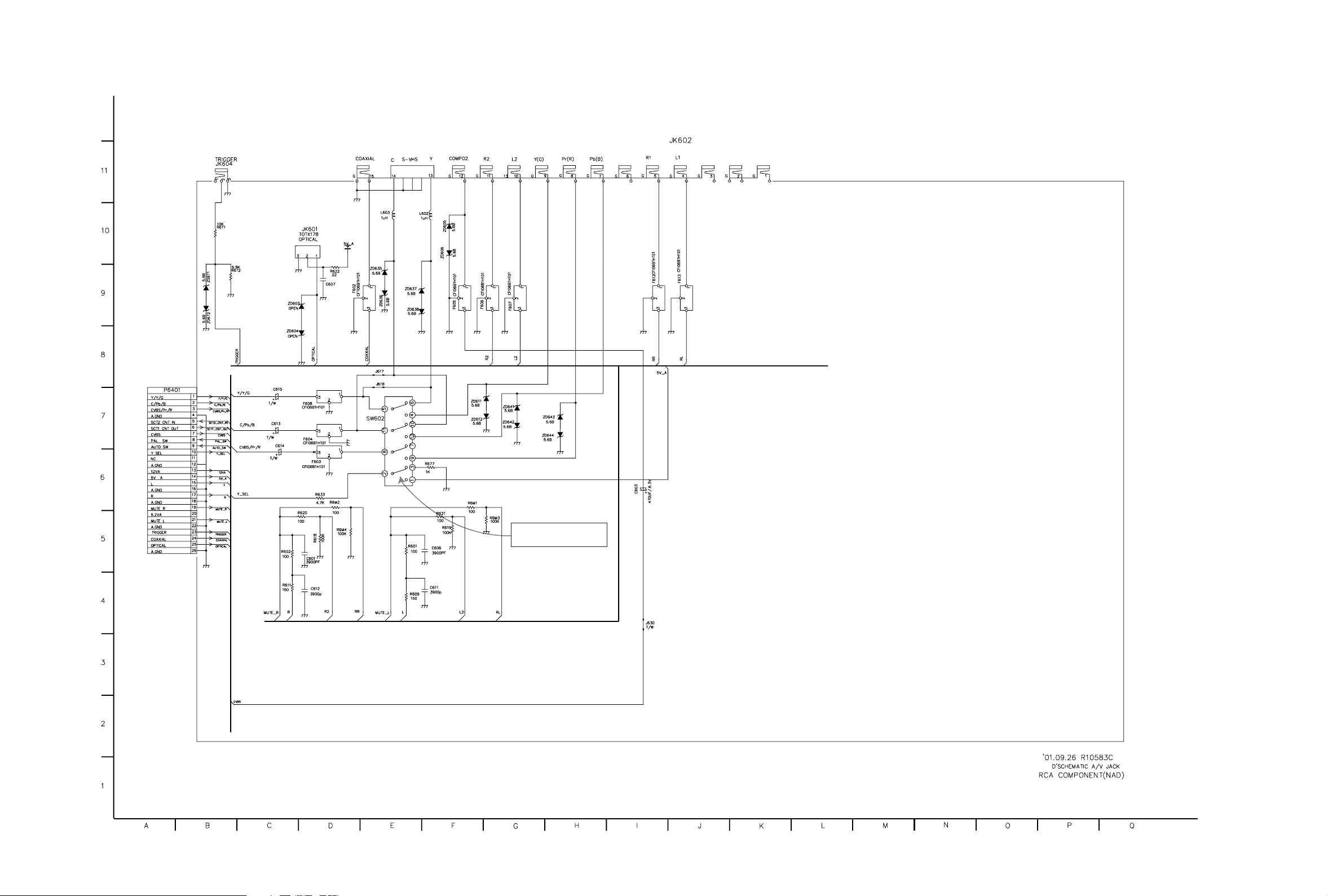
8. A/V JACK CIRCUIT DIAGRAM (T571AH ONLY)
T571C/T571AH
Component, S-Video out
can,t be changed.
Page 11
3-35 3-36
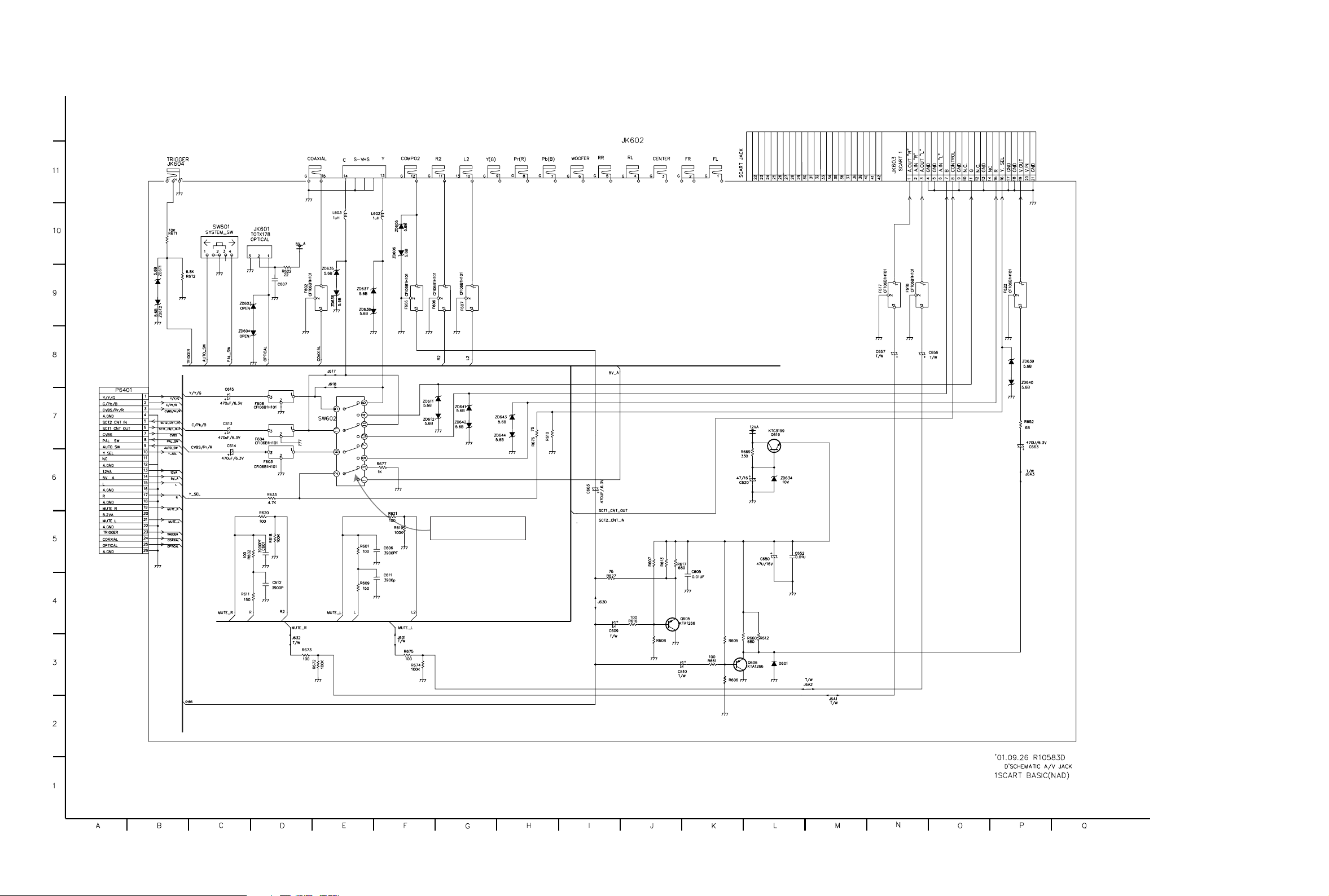
9. SCART CIRCUIT DIAGRAM (T571C ONLY)
T571C/T571AH
Component, S-Video out
can,t be changed.
Page 12
3-37 3-38
LEVEL(V)
MODE
PIN NO.
1
2
3
4
5
6
7
8
9
10
11
12
13
14
15
16
17
18
19
20
21
22
23
24
25
26
27
28
29
30
31
32
33
34
35
36
37
38
39
40
41
42
43
44
45
46
47
48
49
50
51
52
53
3.18
1.3
1.4
2.2
1.5
0
1.5
1.4
1.6
3.1
0.7
0.15
0.15
0
0
1.7
1.4
0
1.5
1.6
0
1.6
0
3.1
1.7
1.4
3.1
1.5
0.15
0
0.7
1.5
2.2
2
3.1
2.9
2.2
2.9
0
0
0
1.6
3.1
1.6
1.5
0
1.4
0
1.5
1.7
1.2
3.1
LEVEL(V)
MODE
PIN NO.
54
55
56
57
58
59
60
61
62
63
64
65
66
67
68
69
70
71
72
73
74
75
76
77
78
79
80
81
82
83
84
85
86
87
88
89
90
91
92
93
94
95
96
97
98
99
100
101
102
103
104
105
106
107
108
1.6
1.4
1.5
0
1.6
1.4
1.5
1.4
3.1
1
1.5
0.005
0.5
0.003
1.58
0
3.1
1.2
1.2
1.2
1.2
3.1
1.65
2.2
1.5
1.5
3.1
3.1
0.001
3.1
3.7
0
3.1
3.1
2.1
0.004
3.1
0
0
0
2.1
3.1
0
0
0
0
2.1
2.1
LEVEL(V)
MODE
PIN NO.
109
110
111
112
113
114
115
116
117
118
119
120
121
122
123
124
125
126
127
128
129
130
131
132
133
134
135
136
137
138
139
140
141
142
143
144
145
146
147
148
149
150
151
152
153
154
155
156
157
158
159
160
161
162
163
0
0.8
0.9
1.3
3.1
0.78
0
1.26
2.38
0.08
1.2
2
0
3.1
3.1
3.1
3.1
0
2.2
3.1
3.1
3.1
3.1
3.1
3.1
3.1
3.1
3.1
3.1
0
3.1
3.1
3.1
3.1
3.1
3.1
3.1
3.1
3.1
3.1
3.1
2.2
1.5
3.1
0
LEVEL(V)
MODE
PIN NO.
164
165
166
167
168
169
170
171
172
173
174
175
176
177
178
179
180
181
182
183
184
185
186
187
188
189
190
191
192
193
194
195
196
197
198
199
200
201
202
203
204
205
206
207
208
209
210
211
212
213
214
215
216
217
218
3.1
3.1
3.1
3.1
3.1
3.1
3.1
0
3.1
3.1
3.1
1.5
3.1
0
3.1
3.1
3.1
3.1
3.18
0.086
3
2.4
2.3
0
0
3.1
0
0.017
2.2
3.1
3.1
0
3.18
1.3
3.1
3.1
3.1
0
2.3
3.1
0.001
3.1
3.1
3.1
1.6
3.1
3.18
0.018
2.2
3.19
2.69
1.5
2.9
2.59
0
LEVEL(V)
MODE
PIN NO.
219
220
221
222
223
224
225
226
227
228
229
230
231
232
233
234
235
236
237
238
239
240
2.29
2.08
2.29
2.29
2.49
3.1
2.39
2.45
1.5
0
1.52
0
1.61
1.6
3.1
1.6
1.6
1.5
0
1.6
1.4
1.5
LEVEL(V)
MODE
PIN NO.
1
2
3
4
5
6
7
8
9
10
11
12
13
14
15
16
17
18
19
20
21
22
23
24
25
26
27
28
29
30
31
32
33
34
35
36
37
38
39
40
41
42
43
44
45
46
47
48
49
50
51
52
53
4.3
3.1
0
3.2
2
3.1
0.01
3.1
3.2
3.2
3.2
3.2
0
3.1
3.1
3.1
0
0
0
3
0.625
3.2
0.705
3.2
3.1
0
3.1
3.1
2.39
3.2
1.49
1.5
3.09
1.69
0
3.1
3.1
2.5
3.1
3.1
3.2
3.1
3.1
LEVEL(V)
MODE
PIN NO.
54
55
56
57
58
59
60
61
62
63
64
65
66
67
68
69
70
71
72
73
74
75
76
77
78
79
80
81
82
83
84
85
86
87
88
89
90
91
92
93
94
95
96
97
98
99
100
3.1
3.1
3.1
3.1
3.1
3.1
3.1
0.5
0
3.1
3.1
3.1
3.1
3.1
1.6
0
0
3.1
0
3.1
0
3.2
0
3.1
0.3
0
0
2.5
0
3.19
3.19
4.4
3.19
4.4
0
4.4
0
0
0
0
0
3.17
3.17
3.1
0
PANTERA MEMORY
IC301IC501
EE PLAY
MODE
PIN NO.
DSP
IC201 SP3301
1
2
3
4
5
6
7
8
9
10
11
12
13
14
15
16
17
18
19
20
21
22
23
24
25
26
27
28
29
30
31
32
33
34
35
36
37
38
39
40
41
42
43
44
45
46
47
48
49
50
51
52
53
2.00
2.00
2.00
2.00
2.00
2.00
2.00
2.00
2.00
2.00
2.00
2.00
2.00
2.00
2.00
2.00
0.00
0.00
0.00
0.00
0.00
3.10
0.00
0.00
0.00
0.00
0.00
2.10
0.00
2.10
3.10
3.10
3.10
3.10
2.10
1.10
0.00
0.00
0.00
3.10
0.00
3.10
0.00
0.00
3.10
0.00
0.00
0.00
0.00
0.00
0.00
3.10
0.00
1.30
1.30
1.30
1.30
1.30
1.30
1.30
1.30
1.30
1.30
1.30
1.30
1.30
1.30
1.30
1.30
0.00
1.50
1.50
1.50
1.50
3.00
1.50
1.50
1.50
1.50
1.50
1.50
0.00
2.00
3.00
1.50
2.50
2.50
1.30
1.80
0.00
0.00
0.00
3.00
0.00
3.00
0.00
0.00
3.00
0.00
0.00
0.00
3.00
0.00
0.00
1.80
0.00
EE PLAY
MODE
PIN NO.
54
55
56
57
58
59
60
61
62
63
64
65
66
67
68
69
70
71
72
73
74
75
76
77
78
79
80
81
82
83
84
85
86
87
88
89
90
91
92
93
94
95
96
97
98
99
100
101
102
103
104
105
106
107
108
3.10
3.10
0.00
0.00
5.00
0.00
0.00
5.00
0.00
2.10
0.00
3.10
0.00
3.10
0.00
0.00
0.00
3.10
0.00
0.00
3.10
0.00
0.00
0.00
0.00
3.10
5.00
0.00
5.00
2.10
2.10
3.10
1.40
0.00
2.10
2.10
0.00
1.50
3.10
1.60
1.10
2.00
1.55
0.00
1.55
1.56
3.10
1.55
1.55
1.62
1.55
1.50
0.00
0.00
0.00
3.00
3.00
0.00
3.13
4.98
0.00
0.00
4.98
0.00
2.10
0.00
3.00
0.00
3.12
0.00
0.20
0.00
3.10
0.20
0.00
3.10
0.00
0.00
0.00
2.30
3.10
5.00
0.00
5.00
2.00
2.10
3.10
1.40
0.00
2.00
2.00
0.00
1.55
3.12
1.55
1.11
2.00
1.55
0.00
1.55
2.15
3.10
1.58
1.55
1.64
1.55
1.50
0.00
0.00
0.00
EE PLAY
MODE
PIN NO.
109
110
111
112
113
114
115
116
117
118
119
120
121
122
123
124
125
126
127
128
129
130
131
132
133
134
135
136
137
138
139
140
141
142
143
144
145
146
147
148
149
150
151
152
153
154
155
156
157
158
159
160
161
162
163
0.00
0.00
0.00
0.00
3.40
5.00
1.50
1.50
3.10
0.00
0.00
3.50
3.25
3.45
3.50
3.50
3.50
0.00
3.60
0.00
3.60
0.00
0.00
0.00
3.10
0.00
0.00
3.10
0.00
0.00
3.10
3.00
0.00
3.00
3.10
3.10
3.10
3.50
0.00
0.00
0.00
0.00
0.00
0.00
0.00
0.00
1.55
3.10
1.50
0.00
0.00
2.60
3.10
2.00
2.00
0.00
0.00
0.00
0.00
4.70
5.00
1.50
1.53
3.10
0.00
0.00
4.20
4.20
4.30
4.30
4.30
4.50
0.00
2.60
0.00
2.60
0.20
0.00
3.10
3.10
0.00
0.00
2.20
0.00
0.00
3.10
3.10
0.00
3.00
3.10
3.10
0.90
4.50
0.00
0.00
0.00
0.00
0.00
0.00
0.00
0.00
1.55
3.10
1.50
0.00
0.00
2.60
3.10
2.00
2.00
• CIRCUIT VOLTAGE CHART
Page 13

3-39 3-40
EE PLAY
MODE
PIN NO.
164
165
166
167
168
169
170
171
172
173
174
175
176
177
178
179
180
181
182
183
184
185
186
187
188
189
190
191
192
193
194
195
196
197
198
199
200
201
202
203
204
205
206
207
208
1
2
3
4
5
6
7
8
1.40
3.20
1.60
0.00
0.00
0.00
5.00
0.00
3.10
3.10
3.10
3.10
2.53
4.24
5.00
2.70
3.26
3.10
2.40
3.66
2.40
0.00
2.26
3.10
2.20
1.75
2.20
1.80
2.20
1.25
1.00
5.00
0.00
0.00
0.00
0.00
0.00
0.00
0.00
0.00
0.00
3.10
1.50
3.10
3.10
3.44
3.12
2.50
2.51
3.50
3.46
3.47
3.47
1.40
0.00
1.75
0.00
3.10
3.10
2.50
2.50
0.00
3.10
3.10
3.10
1.30
4.97
5.00
0.20
2.30
2.50
2.50
2.80
2.50
0.00
2.00
3.10
2.40
1.90
1.80
1.80
2.20
1.30
1.10
5.00
2.25
1.60
1.50
1.50
1.50
1.50
1.50
1.50
1.50
2.60
1.50
3.10
3.10
3.38
3.40
2.50
2.53
3.44
3.44
3.45
3.44
EE PLAY
MODE
PIN NO.
9
10
11
12
13
14
15
16
17
18
19
20
21
22
23
24
25
26
27
28
29
30
31
32
33
34
35
36
37
38
39
40
41
42
43
44
45
46
47
48
49
50
51
52
53
54
55
56
57
58
59
60
61
62
63
3.48
3.43
2.52
2.52
2.52
2.52
2.56
2.48
2.98
0.00
4.50
0.00
0.00
4.96
0.00
4.95
5.00
2.52
1.55
4.97
0.00
2.55
2.51
4.90
0.00
0.00
0.00
1.56
3.58
2.62
0.00
2.50
1.55
1.46
1.58
2.52
4.92
4.99
0.00
0.00
3.59
0.00
2.35
2.37
3.51
3.51
0.61
1.67
2.95
4.98
3.48
3.48
3.71
3.75
0.27
3.44
3.41
2.70
2.70
2.60
2.60
2.70
2.50
3.30
0.00
4.58
0.00
0.20
3.85
0.00
4.92
0.00
2.50
1.55
4.93
0.40
2.63
2.56
4.65
0.20
2.60
2.50
2.15
0.00
3.20
2.60
2.60
1.60
1.65
1.64
2.50
4.97
5.00
0.00
0.00
0.00
0.00
0.00
2.30
3.47
3.46
0.00
2.42
2.88
4.93
3.40
3.40
3.70
3.70
0.36
EE PLAY
MODE
PIN NO.
64 2.40 0.90
SERVO
IC2A1 33P3721
Page 14

3-41 3-42
PRINTED CIRCUIT DIAGRAMS
1. MAIN P.C.BOARD
LOCATION GUIDE
Page 15

3-43 3-44
LOCATION GUIDE
2. AV JACK P.C.BOARD
4. FRONT P.C.BOARD
LOCATION GUIDE
3. SMPS P.C.BOARD
Page 16

CONTENTS
SECTION 1 . . . .SUMMARY
SECTION 2 . . . .CABINET & MAIN CHASSIS
SECTION 3 . . . .ELECTRICAL
SECTION 4 . . . .MECHANISM
SECTION 5 . . . .REPLACEMENT PARTS LIST
Page 17

SECTION 1
SUMMARY
CONTENTS
PRODUCT SAFETY SERVICING GUIDELINES FOR VIDEO PRODUCTS
........................... 1-3
SERVICING PRECAUTIONS .................................................................................................. 1-4
• General Servicing Precautions
• Insulation Checking Prodedure
• Electrostatically Sensitive Devices
SPECIFICATIONS ...................................................................................................................... 1-5
Page 18

1-3
Prior to shipment from the factory, the products are strictly inspected to conform with the recognized product
safety and electrical codes of the countries in which they are to be sold. However, in order to maintain such compliance, it is equally important to implement the following precautions when a set is being serviced.
• Precautions during Servicing
1. Locations requiring special caution are denoted by labels and inscriptions on the cabinet, chassis and
certain parts of the product. When performing service, be sure to read and comply with these and other
cautionary notices appearing in the operation and service manuals.
2. Parts identified by the symbol and shaded (
Y
) parts are critical for safety.
Replace only with specified part numbers.
Note : Parts in this category also include those specified to comply with X-ray emission standards for
products using cathode ray tubes and those specified for compliance with various regulations
regarding spurious radiation emission.
3. Use Specified internal wiring. Note especially:
1) Double insulated wires
2) High voltage leads
4. Use specified insulating materials for hazardous live parts. Note especially:
1) Insulation Tape
2) PVC tubing
3) Spacers
4) Insulation sheets for transistor
5. Observe that wires do not contact heat producing
parts (heatsinks, oxide metal film resistors, fusible
resistors, etc.)
6. Check that replaced wires do not contact sharp edged
or pointed parts.
7. 1) When a power cord has been replaced, check
that A mark is made on the cord, under strain,
near the aperture, and the flexible cord is
subjected 100 times to a pull of 40N for a duration
of 1 second each.
2) During the test, the cord shall not be displaced by
more than 2mm
8. Also check areas surrounding repaired locations.
IMPORTANT SAFETY PRECAUTIONS
Fig. 1
Power cord
Page 19

1-4
Fig. 3
SAFETY CHECK AFTER SERVICING
Examine the area surrounding the repaired location for damage or deterioration. Observe that screws, parts and
wires have been returned to original positions. Afterwards, perform the following tests and confirm the specified
values in order to verify compliance with safety standards.
• Insulation resistance test
confirm the specified insulation resistance or greater between power cord plug prongs and externally exposed
parts of the set (RF terminals, antenna terminals, video and audio input and output terminals, microphone
jacks, earphone jacks, etc.) See table below.
• Dielectric strength test
Confirm specified dielectric strength or greater between power cord prongs and exposed accessible parts of
the set (RF terminals, antenna terminals, video and
audio input and output terminals, microphone jacks,
earphone jacks, etc.) See table below.
• Clearance distance
When replacing primary circuit components, confirm
specified clearance distance (d), (d') between soldered terminals, and between terminals and surrounding metallic parts. See table below.
Table 1 : Ratings for selected areas
* Class II model only.
Note. This table is unofficial and for reference only. Be sure to confirm the precise values for your particular
country and locality.
• Leakage Current test
Confirm specified or lower leakage current between B(earth ground, power cord plug prongs) and externally
exposed accessible parts (RF terminals, antenna terminals, video and audio input and output terminals, microphone jacks, earphone jacks, etc.)
Measuring Method: (Power ON)
Insert load Z between B(earth ground, power cord
plug prongs) and exposed accessible parts. Use an
AC voltmeter to measure across both terminals of
load Z. See figure and following table.
Table 2:Leakage current ratings for selected areas.
Note. This table is for IEC member only. Be sure to confirm the precise values for your particular country and
Note. locality.
Fig. 2
AC Line Voltage
AC Line Voltage
200 to 240 V
100 to 130 V
*200 to 240 V
*100 to 130 V
Europe
Australia
Europe
Australia
Other terminals
Antenna earth
terminals
i
E 0.7m A peak
i E 2m A DC
i E 0.7m A peak
i E 2m A DC
F 10 MΩ/500 V DC
4kV 1 minute
F 6mm(d)
F 8mm(d)
(a Power cord)
Region
Load Z Leakage Current(i)
Earth Ground
(B) to :
Region
Insulation
Resistance
Dielectric
Strength
Clearance
Distance(d),(d)
2k
Ω
50k
Ω
d
Primary circuit terminals
Chassis
a
Exposed
accessible
part
Load
Z
Earth Ground,
Power cord plug prongs
B
AC Voltmeter
Page 20

1-5
SPECIFICATIONS
DVD VIDEO PLAYER
Power supply AC 120 V, 60 Hz (T571AH)
AC 110~240 V, 50/60 Hz (T571C)
Power consumtion 16 W
Mass 5.7 kg(12.6 lbs)
External dimensions 440 x 118 x 423 mm (W x H x D)
Signal system NTSC (T571AH)
PAL (T571C)
Laser (DVD) Semiconductor laser, wavelength 650 nm
(CD) 780 nm
Frequency range (audio) DVD : fs = 96 kHz 4 Hz - 44 kHz
fs = 48 kHz 4 Hz - 22 kHz
CD: 4 Hz - 20 kHz
Signal-to-noise ratio (audio) More than 105dB (EIAJ)
Audio dynamic range (audio) More than 100dB (EIAJ)
Harmonic distortion(audio) 0.003%
Wow and flutter Below measurable level (less than +0.001%(W.PEAK)) (EIAJ)
Operations Temperature : 5˚C(41˚F) to 35˚C(95˚F),
Operation status : Horizontal
OUTPUTS
Video outputs 1.0V(p-p), 75Ω, negative sync., RCA jack x 1/
SCART(TO TV) (T571C ONLY)
S-video outputs (Y)1.0V(p-p), 75Ω, negative sync.,Mini DIN 4-pin x 1
(C)0.286V(p-p), 75Ω
Component video output (Y)1.0V(p-p), 75Ω,negative sync., RCA jack x 1
(Pb)/(Pr) 0.7V(p-p), 75Ω
Audio output(digital audio) 0.5V(p-p), 75Ω, RCA jack X 1/SCART(TO TV) (T571C ONLY)
Audio output(analog audio) 2.0Vrms (1kHz, 0dB), 330Ω, RCA jack (L, R) x 2/
SCART(TO TV) (T571C ONLY)
*Designs and specifications are subject to change without notice.
Page 21

2-1
SECTION 2
CABINET & MAIN CHASSIS
CONTENTS
1. DISASSEMBLY.........................................................................................................................2-2
CABINET DISASSEMBLY ............................................................................................................2-2
CIRCUIT BOARD DISASSEMBLY ...............................................................................................2-3
2. EXPLODED VIEWS ................................................................................................................2-4
1. Cabinet and Main Frame Section...........................................................................................2-4
2. Packing Accessory Section ....................................................................................................2-5
Page 22

2-2
DISASSEMBLY
CAUTION BEFORE STARTING SERVICING
Electronic parts are susceptible to static electricity and may easily and damaged, so do not forget to take a
proper grounding treatment as required.
Many screws are used inside the unit. To prevent missing, dropping, etc. of the screws, always use a
magnetized screw driver in servicing. Several kinds of screws are used and some of them need special
cautions. That is, take care of the tapping screws securing molded parts and fine pitch screws used to secure
metal parts. If they are used improperly , the screw holes will be easily damaged and the parts can not be fixed.
Top Case
(A)
(A)
(A)
(A)
(A)
(A)
(A)
Disc Tray
Tray Door
Front Panel
Stopper
Stopper
CABINET DISASSEMBLY
1. Top Case
1. Release 7 screws (A). (See Fig. 2-1)
2. Lift the top case with holding the back of it,
and remove it in the direction of the arrow.
Fig. 2-1
Fig. 2-2
Fig. 2-3
3. Front Panel
1. Eject the disc tray. (See Fig. 2-2)
2. Remove the tray door. (See Fig. 2-2)
3. Pull the front panel toward you while pressing
5 stoppers to disengage, and remove the front
panel. (See Fig. 2-3)
2.Tray Door
1. Eject the disc tray.
2. Lift up the tray door in the direction of the
arrow.
Page 23

2-3
(L1)
(L1)
(B)
(B)
(C)
(C)
(C)
Power Code
Power
Circuit
Board
Main Chassis
MA Ass'y Dpm1
Bracket Main
Jack Circuit Board
(F)
(F)
(F)
(F)
Main Circuit Board
(B)
(B)
(D)
(E)
(D)
(D)
(D)
(E)
(E)
(B)
(B)
Fig. 2-4
Fig. 2-5
1. Disassemble Main circuit board, Jack
circuit board, Power circuit board and
MD Ass'y DPM1.
1. Remove the top case.(See Fig. 2-1)
2. Remove 10 screws (B).
3. Disassemble Main circuit board and Jack circuit
board from Bracket Main.
4. Unscrew 3 screws(C) at Bracket Main.
5. Disassemble Bracket Main from Main chassis.
6. Unscrew 4 screws(D) at MD Ass'y DPM1.
7. Turn the portion the direction of arrow to move
the Base Assembly Tray in front of you.
8. Release the other 3 screws(E).
9. Disassemble MD Ass'y DPM1 from Main chassis.
10. Unscrew 4 screws(F) at Power circuit.
11. Disassemble power circuit board from Main
chassis.
CIRCUIT BOARD DISASSEMBLY
Note: Before removing the main circuit board, be sure to shortcircuit the laserdiode output land.
After replacing the main circuit board, open the land after inserting the flexible connector.
(Refer to Mechanism Disassembly)
2. Digitron and Key Circuit Board
1. Remove the front panel.(See Fig. 2-3)
2. Release 6 screws (G), and remove the digitron
circuit board.
(G)
(G)
(G)
(G)
(G)
(G)
Page 24

2-4
EXPLODED VIEWS
1. Cabinet and Main Frame Section
465
465
250
462
462
300
465
260
465
A46
A47
463
463
275
463
463
463
467
A48
463
463
463
463
463
A00
A43
280
285
262
452
452
DIG901
PBTOO
283
A
5
4
3
2
1
BCD
Page 25

2-5
2.Packing Accessory Section
BATTERY
808
PACKING SHEET
804
PACKING
OPTIONAL PARTS
803
811
812
OWNER'S MANUAL
810
CABLE SET ASS'Y
801
REMOCON
900
BOX CARTON
802
PACKING
803
Page 26

3-1
SECTION 3
ELECTRICAL
CONTENTS
ELECTRICAL TROUBLESHOOTING GUIDE......................................................................3-2
1. Power(SMPS) Circuit...............................................................................................................3-2
2. µ-com Circuit............................................................................................................................3-3
3. MPEG Circuit............................................................................................................................3-6
4. Front Circuit(Digitron & Key) ................................................................................................3-7
5. RF/Servo Circuit ......................................................................................................................3-8
BLOCK DIAGRAMS..................................................................................................................3-12
1. Overall Block Diagram ..........................................................................................................3-12
2. Power (SMPS) Block Diagram..............................................................................................3-13
3. RF/CD DSP/DVD DSP/DVD servo Block Diagram ..............................................................3-14
4. Audio Block Diagram ............................................................................................................3-15
5. MPEG Block Diagram...........................................................................................................3-16
CIRCUIT DIAGRAMS................................................................................................................3-17
1. Power (SMPS) Circuit Diagram ............................................................................................3-17
2. DVD DSP Circuit Diagram.....................................................................................................3-19
3. Drive & RF Circuit Diagram ..................................................................................................3-21
4. MPEG Circuit Diagram ..........................................................................................................3-23
• WAVEFORMS ...........................................................................................................................3-25
5. Audio DM & 5.1CH Circuit Diagram.....................................................................................3-27
6. TIMER & Key Circuit Diagram ..............................................................................................3-29
7. A/V Circuit Diagram...............................................................................................................3-31
8. A/V Jack Circuit Diagram......................................................................................................3-33
9. SCART Circuit Diagram.........................................................................................................3-35
• CIRCUIT VOLTAGE CHART.........................................................................................................3-37
PRINTED CIRCUIT DIAGRAMS............................................................................................3-41
1. MAIN P.C.BOARD...................................................................................................................3-41
2. AV JACK P.C.BOARD ........................................................................................................... ..3-43
3. SMPS P.C.BOARD..................................................................................................................3-44
4. FRONT P.C.BOARD ................................................................................................................3-43
Page 27

3-2
ELECTRICAL TROUBLESHOOTING GUIDE
No 5V_D
or 5V_A .
No 5.2VA.
Is 5.2VA section working?
(Is the POWER CTL at
Pin6 High/low?)
Is oscillation present at the
Base of Q108?
Replace Q108.
Check D109, C123, R125,
R124.
Replace R102.
Replace BD101.
(Bridge rectifier)
Is R102(R104) normal?
Is about AC 100V app;ied to
IC101 Pin 3.
Check IC101.
Is 5.2V applied to IC102
Pin 1?
Is there a DC voltage at the
(+) terminal of BD101?
Check R127, 128.
(SHUTDOWN CKT)
1. Power(SMPS) Circuit
No FLD
Is 5.2VA section working?
Replace SMPS trans(T101).
Replace the inferior
components.
Are D109, L103 open?
NO
NO
NO
NO
NO
NO
YES
YES
YES
YES
YES
YES
YES
A. B.
NO
NO
Page 28

3-3
Replace Main B/D
Refer to Front Part
Replace IC502
Reconnect it.
2. µ-COM Circuit
A. No Power
Does Logo appear
on the screen?
Is oscillation of
X501 normal?
Are IC501 Pins 193, 808
and 81 normal?
Do “Hello” appear at FLD?
Is P3901
connected normally?
Is P3901 Pin 8, 9, 18 normal?
The waveform
on 3, 5, 7 pin of IC502
normal?
Check the oscillation
Check short.
OK
Replace IC501
or IC306.
Check power.
(Refer to power)
If power is
normal
OK
POWER ON
1
1
YES
YES
YES
YES
NO
YES
YES
YES
A
NO
NO
NO
NO
NO
NONO
YES
A
Page 29

3-4
B. Audio abnormal
D. Open/Close abnormal
Check the
connection of P3901.
Check IC301 Pins 93, 94.
Check Audio jack.
YES (If OK)
YES
NO
NO
YES
YES
(If OK)
YES
YES
(If OK)
YES (If OK)
YES (If OK)
Refer to Audio part.
Refer to Decoder part.
Refer to PANTERApart.
Replace B/D.
Check Front.
Reconnect it.
Refer to SERVO part.
Check the connection of MD.
AUDIO ABNORMAL
OPEN/CLOSE ABNORMAL
C. Video abnormal
Check Video jack.
YES (If OK)
YES (If OK)
YES (If OK)
Refer to Video part.
Refer to PANTERApart.
Replace B/D.
VIDEO ABNORMAL
Page 30

3-5
E. Picture abnormal
Check the disc.
If OK
YES (If OK)
YES (If OK)
Refer to Servo part
Check DSP
Check PANTERA
Replace B/D
PICTURE ABNORMAL
F. Disc Error
Check Disc
YES (If OK)
YES (If OK)
Refer to Servo part
Replace B/D
DISC ERROR
Page 31

3-6
Power is on
Does TOSHIBA Logo appear
on the screen?
Does the
moving picture of the DVD Disc
play on the screen
normally?
Is PANTERA
data signal normal?
Is error signal normal?
Is PANTERAdata
signal normal?
Is Clock normal?
Does the audio
sound output from PANTERA
decoder?
Does the
moving picture of the video
CD play on the screen
normally?
Does the audio sound
output normally?
END
Check power & clock.
Check CD/DVD DSP output
signal.
Check CD/DVD DSP output
signal.
Check CD/DVD DSP output
signal.
Check clock signal
Check clock signal
YES
YES
YES
YES
YES
YES
YES
YES
YES
YES
NO
NO
NO
OK
NO
NO
NO
NO
NO
3. PANTERA Circuit
_ OPTION
_ If included VCD function.
Page 32

3-7
NO
NO
NO
START
Does remote control
work normally?
Do all the
buttons work
normally?
Check waveform of
IC901 Pin 21, 22.
Check waveform
of IC901 Pin 27.
Is Digitron on normally?
LED ON?
Check waveform
of IC901 Pin 6.
Is oscillation of
X901 normal?
Is waveform of IC901
Pin 40 normal?
Check waveform
of IC901 Pin 22.
Does pulse
waveform of RC901 Pin 1
appear?
Is IC901
Pin 17 connected to
RC901 Pin 1 ?
Is RC901 Pin 2 5V?
Power on.
Check and replace
R926, R925.
Solder defective parts again.
Solder defective parts
Replace IC901.
Solder Key part.
Check Power.
Replace IC902.
Replace IC901.
Replace LED901.
Replace RC901.
Re-solder.
Recheck
Replace IC901.Complete repairing Front B/D.
NO
NO
NO
NO
NO
NONONO
NO
YES
YES YES
YES
YES YES
YES
YES
YES
YES
YES
YES
YES
YES
YES
YES
CD
4. Front Circuit (Digitron & key)
Page 33

3-8
Does signal pulse
input to IC201 Pins 58, 59 when
the power is on?
Does signal goes
"High" to IC201 Pin194 when the
power is on?
Does
TTL pulse output to
IC201 Pins 140, 142?
Does
33.8688MHz clock input
to IC201 Pin 63?
Is IC201
Pins 83, 84, 88, 89 voltage
about 2.2V?
Replace IC201
(IC206 soldering or IC defect).
Check power circuit.
Check "2.PANTERAPart".
Replace X201 or IC206
(30MHz clock defect)
CHECK POINT(General)
5. RF/Servo Circuit
A.
END
NO
NO
NO NO
NO
YES
YES
YESYES
YES
Page 34

3-9
Does tray open or close?
Does the pick-up
slide inner or outer
track?
Fig.1. SLED Driver waveform
Fig.2. Focus Driver waveform
Does
the voltage change
at PMD03 Pins 15, 16 more than
2V on the basis of
3.8V?
Pressing
the open/close key
repeatedly, check the voltage of IC2M1
Pins 13, 14 change
0V to 5V
Does
PMD03 Pin 6 change
high to low?
Does
the pick-up lens move up
and down?
Check Focus Driver output.
(IC201 Pin 83, IC2M1 Pins 37, 38)
Check SLED Driver output.
IC201 Pin 88 IC2M1 Pins 28, 29.
IC201 Pin 88 no output : IC201 is defective
IC2M1 Pins 28, 29 no output : IC2M1 is defective
IC201 Pin 83 no output : IC201 is defective
IC2M1 Pins 37,38 no output : IC2M1 is defective
DECK assembly is defective.
Slide the pick-up to
inner track.
Power on
Check loading Part.
Push Pick-up to inner track to
the end by hand.
DECK assembly is defective.
(Limit sw)
check PANTERAPart.
Replace IC2M1.
No disc
B.
END
NO
NO
NO
NO
NO
NO
YES
YES
YES
YES
YES
YES
Page 35

3-10
FOCUS ON?
Check
the focus error moving the
lens up and down.
(IC2A1 Pin 42)
Does the
TTL level change at IC201
Pin 78 and 132 moving
the lens?
Does the disc turn?
IC201 Pin169 is "High"?
Is OK the track jump.
Does the signal
pulse appear at IC2A1 Pins
39, 29?
Does the screen appear?
OPEN/CLOSE
Replace IC501 or IC201.
Replace IC201.
Check IC2A1 Pin 11,12,13,14
in DVD Mode
Fig.3. FOCUS ERROR waveform
IC201 no output : Pick-up is defective.
Check IC201 and IC2M1 when PMD03 Pin 5 is abnormal
Check IC2M1 Pin 21, PMD03
Pin 5 turn when the IC2M1
Pin 21 is less than 2.2V.
Check A
Video Part is defective.
Check "PANTERACircuit."
Check "7.OSD/Video Circuit."
Replace PANTERApart.
IC2A1 is defective.
DISC IN
C.
END
NO
NO
NO
NO NO
NO
NO
NO
YES
YES
YES
YES
YES
YES YES
YES
Page 36

3-11
See the eye-pattern vivid?
Does the
sawtooth waveform emit
at IC2A1 Pin 41?
Does the 1.6V emit?
Check RF Eye-Pattern.
RF : 1.5-1.6V(IC2A1 Pin 57)
Fig.5. RF
waveform
Check IC2A1 Pins 5, 6, 7, 8.
No signal: Pick-up is defective
Replace IC201.
Check IC201 Pin84.
No signal at IC201 : IC201 is defective
• Check IC201 Pin 162.
• Check the clock at the IC201 Pins 28, 30.
• Both are normal : IC201 is defective
Replace IC2A1.
CHECK A
D.
END
NO
NO NO NO
YES
YES YES YES
Page 37

3-12
BLOCK DIAGRAMS
1. Overall Block Diagram
M
M
DISC
SPINDLE
MOTOR
LOADING
MOTOR
DECK M ECHANISM
CD: A,B, E, F
DVD: A,B,C,D,
DVD; RF
CD: A,B, E, F
DVD: A,B,C,D,
DVD; RF
PICK
UP
IC205
DRAM
16bit
4M
IC201
HY25D801C
CD / DVD DSP
IC501
PANTERA -II/2E
IC901
Upd78032
FROM
FL DISPLAY
KEY Input
REMOCON
RECEIVER
5MHz
X-TAL
Pb
IC301
XC9572VL
CPLD
I/O PORT 72
IC304
SDRAM
16/32BIT
64M
IC502
93C46
EEPROM
IC2M1
KA3032
MOTOR
DRIVER
IC2A1
TA33P3721
RF
ICDATA
[00:15]
ICADD
[0:8]
LOADING
FOCUS,TRA CKING,SLED
SPINDL E
MIRR,TZC,PI,TE
FE,DFECT_IN
RFO
SCLK,SDATA
SCOR,SQCK,SQSO
XLAT,E_STI ,E_ENB,E_DR
RF_XLAT , LDON
IC401
PCM1716
DAC
XIO1,XIO2
,XIO10
F_CLK
F_OUT
PCMCLK
SPINDLE_FG
MSDATO
MDP1
FOK
DEFECT
DSP_SENSE
LOCK
E_SOUT
ZISENB
/XRST
DAC_RST
16
:9,PAL_SW ,AUTO_SW,MIC_ON
Y_SEL
/A_MUTE
/DAC_CS1
/DAC_CS2
V_MUTE
DAC_CLK
DAC_OUT
ADCCLK
ACT_MUTE , LOAD_OPEN , LOAD_CLOSE
MIRR
AD[00:19]
PSENB
FLD
/FLD_CS
FLD_CLK
FLD_OUT
/FLD_CS
COMM_CLK
COMM_OUT
CPLD
EE_CS , EE_CLK , EE _OUT
F_IN
IC3F1
FLASH
ROM
F_IN
/MRESET
74573
/FLASH_CS, /RDPWEO
LA0
LA1
LA2
LA3
ALE
AD[
04:19
]
LADD
[04:19]
MD[00:31]
MCLK2
CKE
MA[00:10]
MA12,13
/CS0
/RAS
/CAS
/WE
DQM0`3
REQP
SDCLKI , PSYNC
DVD[1:7]
DSP_INT
SENSE
/DSP_CS
LRCK
DAC-CS
AOUT3
L
Compos ite
FILTER
Y
Pr
SW602
Video SW
CVBS/Pr/R , C/Pb/, Y/G
Y
C
L/R
-VF
AC 240V,
60Hz
POWER
BOARD
-VF
-24VA
+8V
+5.2VA
+5V_D
+5V_A
+12VA
+3.3V_M
AD[0:7]
LADD4~5 , LA0~3
AD[00:15]
MDP,FDO,TDO,FMO,MON
OPEN_SW
CLOSE_SW
LIMIT_SW
CPLD
SBA DD ,
27MHz
X-TAL
33.8688MHz
X-TAL
+3.3V
POWER_CTL
/SRST
R
AMP
Page 38

3-13
2. Power(SMPS) Block Diagram
5V_D
5V_A
-27VA
VF+
RECTIFIER
LINE FILTER
SWITCHING TR
TRANS
FEED B.
REG(8V)
8V
5.2VA
VF-
RECTIFIER(FLD)
RECTIFIER(9V)
RECTIFIER(5.2V)
LPF
LPF
RECTIFIER(14V)
LPF
12VA
PWR ON/OFF
REG(3.3V)
REG(3.3V)
3.3V
3.3V,3.3V_M
RECTIFIER(3.8V) LPF
-12VA
Page 39

3-14
88
SENS, FOK, SLD_FG,
MSDAT0, DEFECT,DSP_SENSE
IC2M1
KA3017
SpindleMotor,LoadingMotor,
Actuator Driver
CD: A,B,C,D / E, F
44
44
MIRR,TZC
88
55
33
33
SQSO, SQCK,
SCOR
SCOR
66
XLAT, S_CLK, S_DATA
UCOM
I/F
focus, tracking, loading, sled
Spindle
M/D
PICK
UP
MCK
IC206
DVDSP-3301
CD / DVD DSP
DVD SERVO
IC2A1
33P3721
RF Signal
Processor
FDO,TDO,FMO
Load open/close(loading control)
UCOM
I/F
DVD: A,B,C,D,
FE,TE,PI,SBADD
44
DVD/CD RF
DRAM
256K x 16bit
16
9
ICADDR[0:8]
ICDATA[00:15]
DO[0:7]
AO[0:5]
DVD_DATA[0:7]
MON,MDP
SPINDLE_FG
MPEG
I/F
22
DSP_CS, /WR, /RD33
88
3. RF/CD DSP/DVD DSP/DVD SERVO Block Diagram
Page 40

3-15
4. Audio Block Diagram
IC401
PCM1716
Audio DAC
IC402
LPF & Buffer
NJM4580D
OP AMP
U-COM
I/F
A_0WT3
/SRST
DAC
COMM_DATA
COMM_CLK
DAC_CS
LRCK
DA_BCK
DA_XCK
L
R
L
R
MPEG
I/F
Page 41

3-16
5. MPEG Block Diagram
IC501
PANTERA-2
IC301
XC9572VL
CPLD
I/O PORT 72
IC304
SDRAM
16/32BIT
64M
IC502
93C46
EEPROM
IC3F1
FLASH
MEMORY
IC302/IC303
LATCH
AD[0:7] 8
DSP
I/F
DVD[0:7]
8
LA[0:3]
4
SCLK,SDATA
SQCK,SQS0
REQP
SDCLK1,PSYNC
DSP_INT
SENSE
/DSP_CS
AD[00:19]
RF &
MOTOR
I/F
MIRR
LDON
S
C
L
K
,
S
D
A
T
A
EE_CS
F_IN
32
MD[00:31]
MCLK2
CKE
MA[00:10]
MA12,13
/CS0
/RAS/
/CAS
/WE
/DQM[0:3]
SPINDLE_FG
ALE
AD[04:19]
16
LADD[04:19]
16
LA[0:3]
4
AD[00:15]
16
AUDIO
I/F
DA_DATA
DA_BCK,DA_LRCK,DA_XCK
DAC_L0,DAC_L1
DAC_RST
A/V
JACK
I/F
C/R(B)
CVBS/G(R)
Y/B(G)
CVBS
V_MUTE,16:9
ZISENB
/RD
/PWED
 Loading...