

Page 1

SERVICE MANUAL
MODELS : T517C/T517CT SERVICE MANUAL
© NAD 2008
NAD ELECTRONICS INTERNATIONAL
TORONTO
SERVICE MANUAL
T517AH/T517AHT
T517C/T517CT/
DVD VIDEO PLAYER
T517C/T517CT/
T517C/T517CT
DVD VIDEO PLAYER
T517AH/T517AHT
DVD VIDEO PLAYER
Page 2

CONTENTS
SECTION 1.........SUMMARY
SECTION 2.........CABINET & MAIN CHASSIS
SECTION 3.........ELECTRICAL
SECTION 4.........MECHANISM (DP-12V)
SECTION 5.........REPLACEMENT PARTS LIST
Page 3

SECTION 1
SUMMARY
CONTENTS
PRODUCT SAFETY SERVICING GUIDELINES FOR DVD PRODUCTS..................................1-3
SERVICING PRECAUTIONS....................................................................................................................1-4
• GENERAL SERVICING PRECAUTIONS
• INSULATION CHECKING PRODEDURE
• ELECTROSTATICALLY SENSITIVE (ES) DEVICES
THE PROCESS OF DISC DOWNLOAD ...............................................................................................1-5
SPECIFICATIONS ........................................................................................................................................1-7
1-2
Page 4
PRODUCT SAFETY SERVICING GUIDELINES FOR DVD PRODUCTS
IMPORTANT SAFETY NOTICE
This manual was prepared for use only by properly trained audio-video service
technicians.
When servicing this product, under no circumstances should the original design be
modified or altered without permission from NAD. All components should be replaced
only with types identical to those in the original circuit and their physical location, wiring
and lead dress must conform to original layout upon completion of repairs.
Special components are also used to prevent x-radiation, shock and fire hazard.
These components are indicated by the letter “x” included in their component
designators and are required to maintain safe performance. No deviations are allowed
without prior approval by NAD.
Circuit diagrams may occasionally differ from the actual circuit used. This way,
implementation of the latest safety and performance improvement changes into the set
are not delayed until the new service literature is printed.
CAUTION
customized installations without manufacturer’s approval. Unauthorized modifications
will not only void the warranty, but may lead to property damage or user injury.
Service work should be performed only after you are thoroughly familiar with these
safety checks and servicing guidelines.
GRAPHIC SYMBOLS
SERVICE INFORMATION
While servicing, use an isolation transformer for protection from AC line shock. After the
original service problem has been corrected, make a check of the following:
FIRE AND SHOCK HAZARD
1. Be sure that all components are positioned to avoid a possibility of adjacent
2. Verify that all protective devices such as insulators, barriers, covers, shields, strain
3. Soldering must be inspected to discover possible cold solder joints, solder splashes,
4. Check for physical evidence of damage or deterioration to parts and components,
5. No lead or component should touch a high current device or a resistor rated at 1 watt
6. After reassembly of the set, always perform an AC leakage test on all exposed
: Do not attempt to modify this product in any way. Never perform
The exclamation point within an equilateral triangle is intended to alert
the service personnel to important safety information in the service
literature.
The lightning flash with arrowhead symbol within an equilateral triangle
is intended to alert the service personnel to the presence of noninsulated
“dangerous voltage” that may be of sufficient magnitude to constitute a
risk of electric shock.
The pictorial representation of a fuse and its rating within an equilateral
triangle is intended to convey to the service personnel the following fuse
replacement caution notice:
CAUTION: FOR CONTINUED PROTECTION AGAINST RISK OF
FIRE, REPLACE ALL FUSES WITH THE SAME TYPE AND RATING
AS MARKED NEAR EACH FUSE.
component shorts. This is especially important on items trans-ported to and from the
repair shop.
reliefs, power supply cords, and other hardware have been reinstalled per the
original design. Be sure that the safety purpose of the polarized line plug has not
been defeated.
or sharp solder points. Be certain to remove all loose foreign particles.
for frayed leads or damaged insulation (including the AC cord), and replace if
necessary.
or more. Lead tension around protruding metal surfaces must be avoided.
metallic parts of the cabinet (the channel selector knobs, antenna terminals, handle
and screws) to be sure that set is safe to operate without danger of electrical shock.
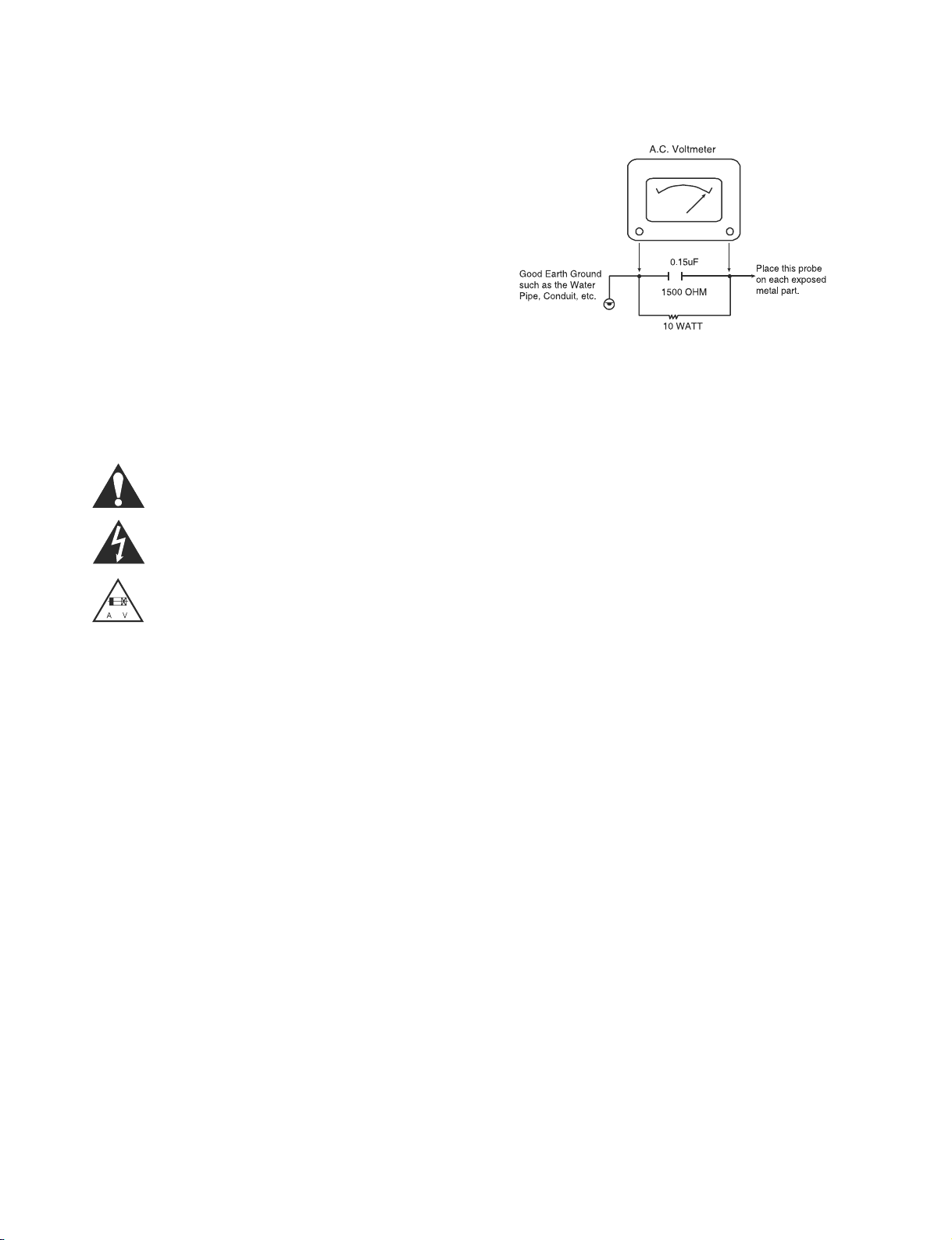
DO NOT USE ALINE ISOLATION TRANSFORMER DURING THIS TEST. Use an
AC voltmeter having 5000 ohms per volt or more sensitivity in the following manner:
Connect a 1500 ohm, 10 watt resistor, paralleled by a .15 mfd 150V AC type
capacitor between a known good earth ground water pipe, conduit, etc.) and the
exposed metallic parts, one at a time. Measure the AC voltage across the
combination of 1500 ohm resistor and .15 mfd capacitor. Reverse the AC plug by
using a non-polarized adaptor and repeat AC voltage measurements for each
exposed metallic part. Voltage measured must not exceed 0.75 volts RMS. This
corresponds to 0.5 milliamp AC. Any value exceeding this limit constitutes a potential
shock hazard and must be corrected immediately.
TIPS ON PROPER INSTALLATION
1. Never install any receiver in a closed-in recess, cubbyhole, or closely fitting shelf
space over, or close to, a heat duct, or in the path of heated air flow.
2. Avoid conditions of high humidity such as: outdoor patio installations where dew is a
factor, near steam radiators where steam leakage is a factor, etc.
3. Avoid placement where draperies may obstruct venting. The customer should also
avoid the use of decorative scarves or other coverings that might obstruct ventilation.
4. Wall- and shelf-mounted installations using a commercial mounting kit must follow
the factory-approved mounting instructions. A product mounted to a shelf or platform
must retain its original feet (or the equivalent thickness in spacers) to provide
adequate air flow across the bottom. Bolts or screws used for fasteners must not
touch any parts or wiring. Perform leakage tests on customized installations.
5. Caution customers against mounting a product on a sloping shelf or in a tilted
position, unless the receiver is properly secured.
6. A product on a roll-about cart should be stable in its mounting to the cart.
Caution the customer on the hazards of trying to roll a cart with small casters across
thresholds or deep pile carpets.
7. Caution customers against using extension cords. Explain that a forest of
extensions, sprouting from a single outlet, can lead to disastrous consequences to
home and family.
1-3
Page 5

SERVICING PRECAUTIONS
CAUTION: Before servicing the DVD covered by this service
data and its supplements and addends, read and follow the
SAFETY PRECAUTIONS. NOTE: if unforeseen circumstances
create conflict between the following servicing precautions
and any of the safety precautions in this publication, always
follow the safety precautions.
Remember Safety First :
General Servicing Precautions
1. Always unplug the DVD AC power cord from the AC power
source before:
(1) Removing or reinstalling any component, circuit board,
module, or any other assembly.
(2) Disconnecting or reconnecting any internal electrical
plug or other electrical connection.
(3) Connecting a test substitute in parallel with an
electrolytic capacitor.
Caution: A wrong part substitution or incorrect polarity
installation of electrolytic capacitors may result in an
explosion hazard.
2. Do not spray chemicals on or near this DVD or any of its
assemblies.
3. Unless specified otherwise in this service data, clean
electrical contacts by applying an appropriate contact
cleaning solution to the contacts with a pipe cleaner, cottontipped swab, or comparable soft applicator.
Unless specified otherwise in this service data, lubrication of
contacts is not required.
4. Do not defeat any plug/socket B+ voltage interlocks with
which instruments covered by this service manual might be
equipped.
5. Do not apply AC power to this DVD and / or any of its
electrical assemblies unless all solid state device heat sinks
are correctly installed.
6. Always connect the test instrument ground lead to an
appropriate ground before connecting the test instrument
positive lead. Always remove the test instrument ground
lead last.
Insulation Checking Procedure
Disconnect the attachment plug from the AC outlet and turn
the power on. Connect an insulation resistance meter (500V)
to the blades of the attachment plug. The insulation resistance
between each blade of the attachment plug and accessible
conductive parts (Note 1) should be more than 1Mohm.
Note 1: Accessible Conductive Parts include Metal panels,
Input terminals, Earphone jacks,etc.
Electrostatically Sensitive (ES) Devices
Some semiconductor (solid state) devices can be damaged
easily by static electricity. Such components commonly are
called Electrostatically Sensitive (ES) Devices. Examples of
typical ES devices are integrated circuits and some field effect
transistors and semiconductor chip components.
The following techniques should be used to help reduce the
incidence of component damage caused by static electricity.
1. Immediately before handling any semiconductor component
or semiconductor-equipped assembly, drain off any
electrostatic charge on your body by touching a known earth
ground. Alternatively, obtain and wear a commercially
available discharging wrist strap device, which should be
removed for potential shock reasons prior to applying power
to the unit under test.
2. After removing an electrical assembly equipped with ES
devices, place the assembly on a conductive surface such
as aluminum foil, to prevent electrostatic charge buildup or
exposure of the assembly.
3. Use only a grounded-tip soldering iron to solder or unsolder
ES devices.
4. Use only an anti-static solder removal device. Some solder
removal devices not classified as “anti-static” can generate
electrical charges sufficient to damage ES devices.
5. Do not use freon-propelled chemicals. These can generate
an electrical charge sufficient to damage ES devices.
6. Do not remove a replacement ES device from its protective
package until immediately before you are ready to install it.
(Most replacement ES devices are packaged with leads
electrically shorted together by conductive foam, aluminum
foil, or comparable conductive material).
7. Immediately before removing the protective material from
the leads of a replacement ES device, touch the protective
material to the chassis or circuit assembly into which the
device will be installed.
Caution: Be sure no power is applied to the chassis or
circuit, and observe all other safety precautions.
8.Minimize bodily motions when handling unpackaged
replacement ES devices. (Normally harmless motion such
as the brushing together of your clothes fabric or the lifting
of your foot from a carpeted floor can generate static
electricity sufficient to damage an ES device.)
1-4
Page 6
THE PROCESS OF DISC DOWNLOAD
Please follow the below process to download a program with disc
1. Turn on the DVD-player.
(Note. Be sure that there is no disc in DVD-player)
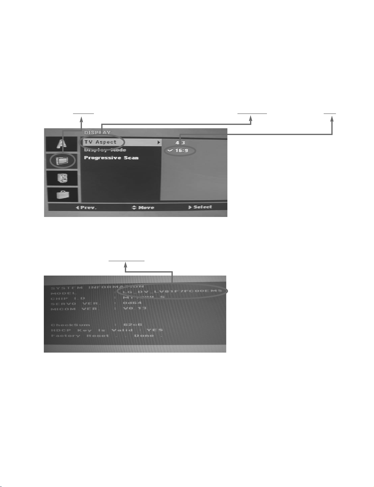
2. Press “SETUP” button on Remote control.
3. Choose a “display” menu by using the cursor button and then choose a “TV Aspect” menu. And choose “16:9”
menu.
4. Press the 1 --> 3 --> 9 --> 7 --> 1 --> 3 --> 9(numerical button) --> Enter key on remote control to confirm the
system information.
5. Remember or write the model name.
6. Change the program file name of new version to the model name
Ex> New ver. program file->LG_DV_LV80F7FC10EMSMIS_V014.ROM
Model name -> LG_DV_LV81F7FC00EMS
Change New ver. program file like this --> LG_DV_LV81F7FC00EMSMIS.ROM
(NOTICE) You must add “MIS” at the end of model name
If you don”t change the file name like that, Disc download isn”t be worked.
1-5
Page 7
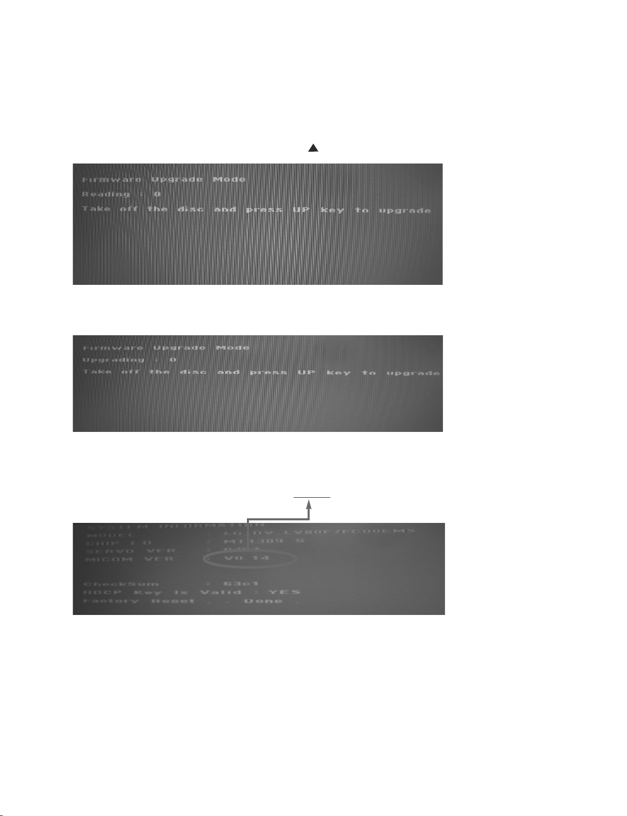
7. Copy the changed file to a disc.
8. Insert the copied disc to DVD-player.
9. If the below picture appears on the screen, Press “ ” key.
10.After the below picture appears on the screen, Disc will emerge from DVD-player automatically.
Take the disc out of the DVD-player.
11.After Disc download is completed, DVD-player turns off and then turns on automatically.
12.Do it again the process 1, 2, 3, 4 to confirm the version.
1-6
Page 8

SPECIFICATIONS
• GENERAL
Power requirements: AC 100 V ~ 240 V, 50 Hz / 60 Hz
Power consumption: 9 W
Dimensions (Approx.): 430 x 39 x 192 mm (17 x 1.5 x 7.6 inches) (W x H x D) without foot
Net weight (Approx.): 1.5 kg (3.3 lbs)
Operating temperature: 5 °C to 35 °C (41 °F to 95 °F)
Operating humidity: 5 % to 90 %
• OUTPUTS
VIDEO OUTPUT: 1.0 V (p-p), 75 , sync negative, RCA jack x 1 / Scart (to TV)
S-VIDEO OUTPUT: (Y) 1.0 V (p-p), 75 , negative sync, Mini DIN 4-pin x 1
(C) 0.3 V (p-p) 75
COMPONENT VIDEO OUTPUT: (Y) 1.0 V (p-p), 75 , negative sync, RCA jack x 1
(Pb)/(Pr) 0.7 V (p-p), 75 , RCA jack x 2
HDMI OUTPUT (Video/Audio): 19 pin (HDMI standard, Type A)
AUDIO OUTPUT: 2.0 Vrms (1 kHz, 0 dB), 600 , RCA jack (L, R) x 1 / Scart (to TV)
DIGITAL AUDIO OUTPUT: COAXIAL: 0.5 V (p-p), 75 , RCA jack x 1
OPTICAL: 3 V (p-p), Optical jack x 1
• SYSTEM
Laser: Semiconductor laser, wavelength 650 nm
Signal system: PAL
Frequency response: DVD (PCM 96 kHz): 8 Hz to 44 kHz
DVD (PCM 48 kHz): 8 Hz to 22 kHz
CD: 8 Hz to 20 kHz
Signal-to-noise ratio: More than 90 dB (ANALOG OUT connectors only)
Harmonic distortion: Less than 0.02 %
Dynamic range: More than 95 dB (DVD/CD)
1-7
Page 9

MEMO
1-8
Page 10

SECTION 2
CABINET & MAIN CHASSIS
CONTENTS
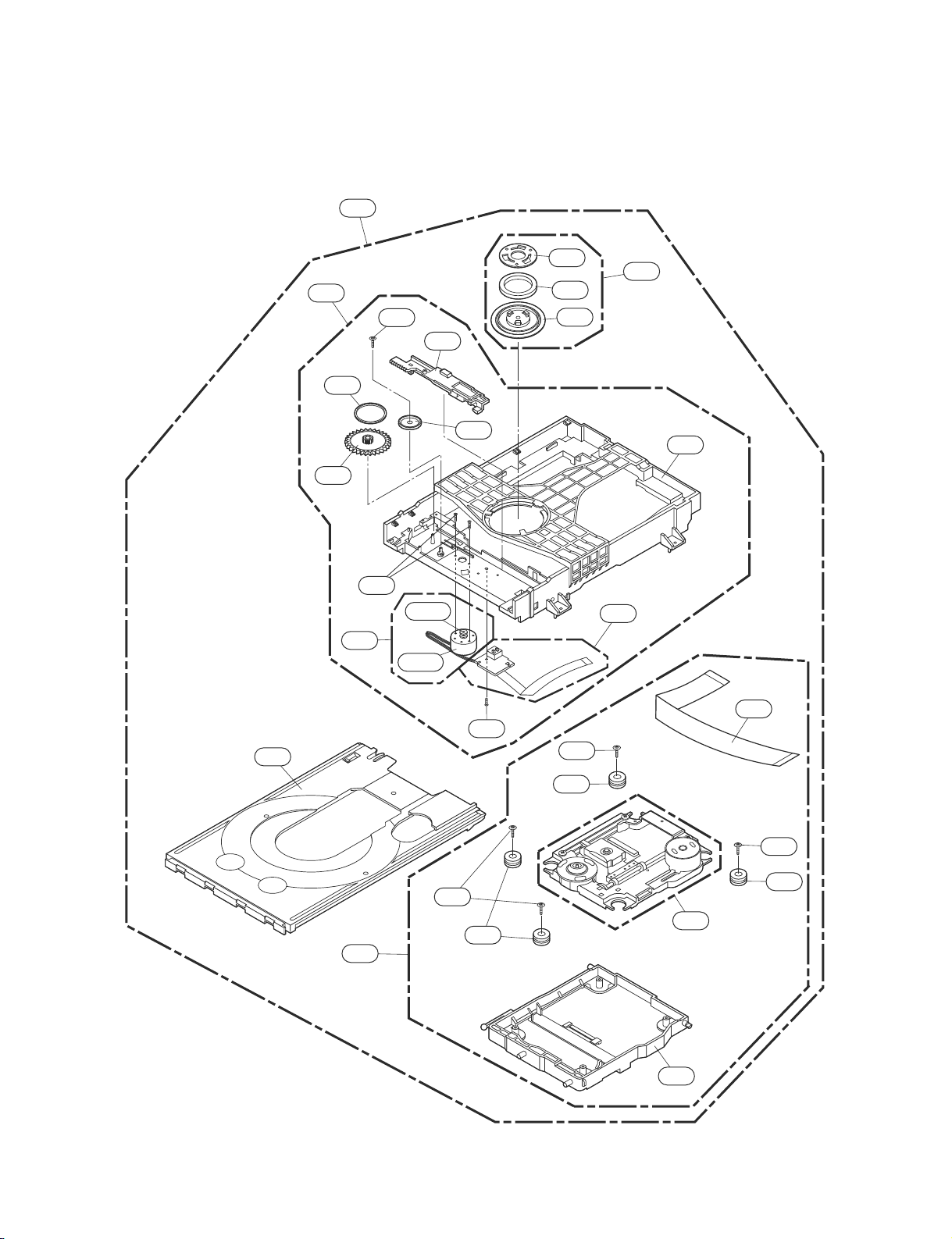
EXPLODED VIEWS .....................................................................................................................................2-2
1. CABINET AND MAIN FRAME SECTION ..................................................................................................2-2
2. DECK MECHANISM SECTION (DP-12V).................................................................................................2-3
3. PACKING ACCESSORY SECTION...........................................................................................................2-4
2-1
Page 11
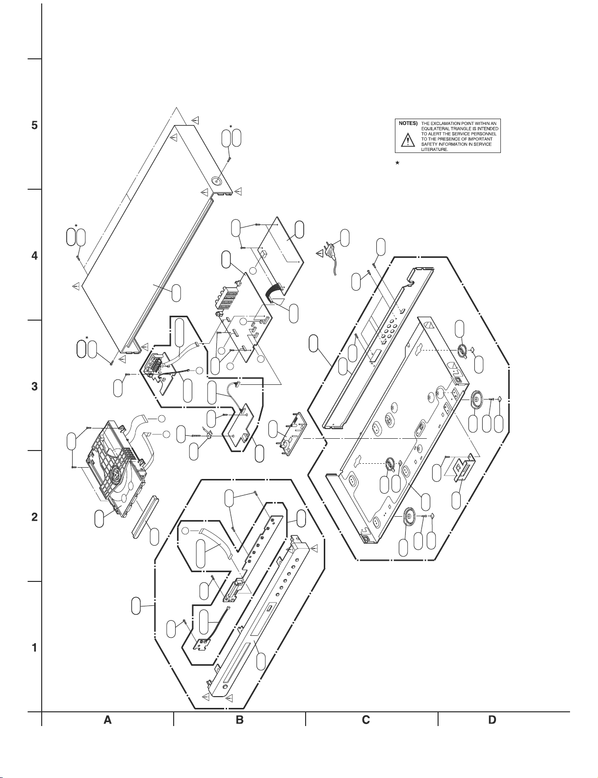
EXPLODED VIEWS
1. CABINET AND MAIN FRAME SECTION
60
463
4
OPTIONAL PART
3
46346346
462
460
3
3
46346346
46346
460
462
462
A46
A
250
MAIN
E
CABLE2
CART
P3702
S
B
C
461
B
62
C
4
E
N801
C
463
5
27
52
4
D
USB
A41
SMPS
276
A47
P101
100V~240V
POWER CORD
A44
20
3
300
467
465
470
261B
261
260
261B
261
62
4
261
261A
62
4
262
A26
A43
283
D
A50
62
261
4
261A
CABLE1
452
52
4
CN903
KEY
TIMER
80
2
2-2
Page 12
2. DECK MECHANISM SECTION (DP-12V)
A26
026
A02
017
013
015
435
439
015B
015A
001
A01
002
003
018
014
020
016
010
440
442
A03
012
442
012
442
037
012
019
2-3
Page 13
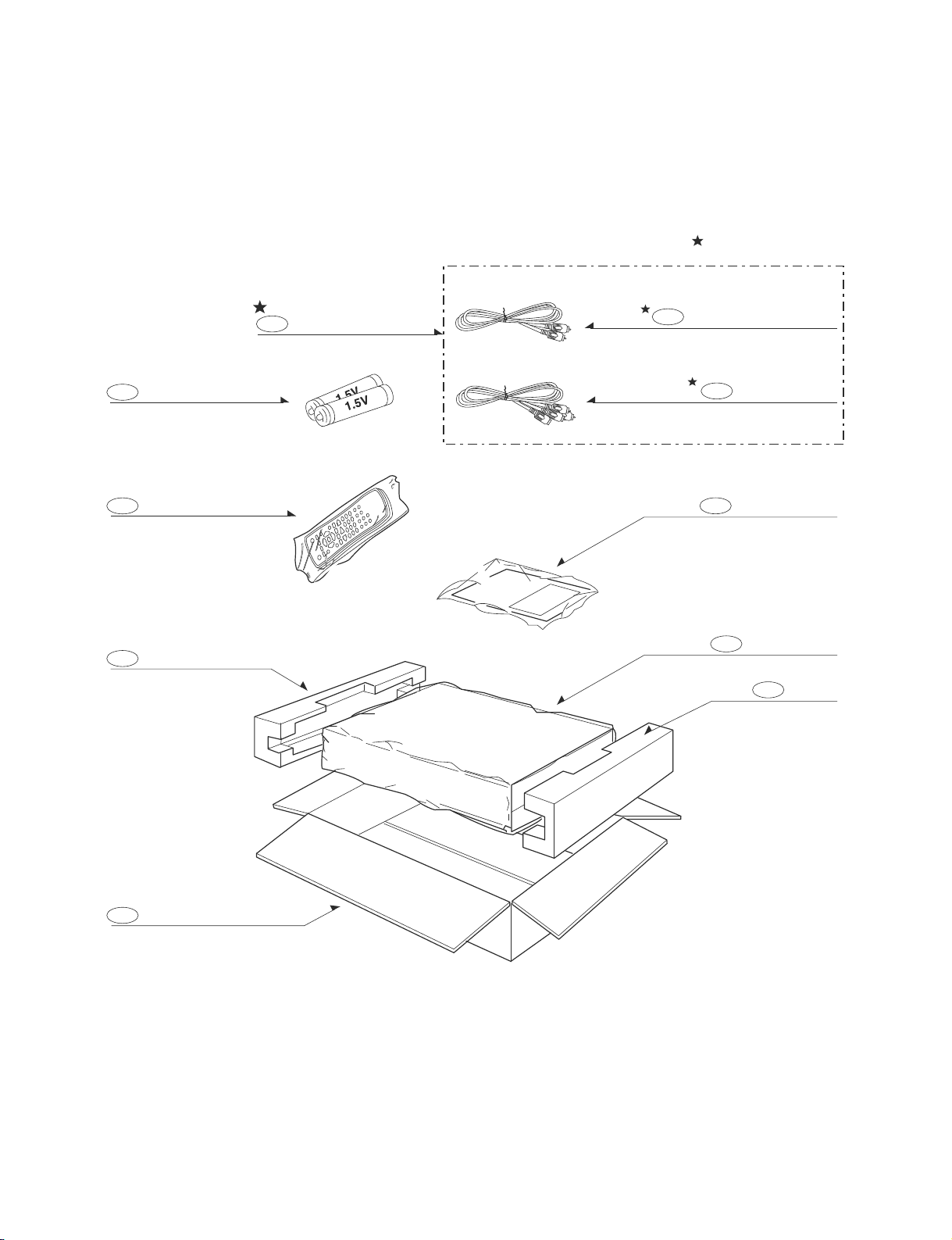
3. PACKING ACCESSORY SECTION
OPTIONAL PARTS
808 Battery
900 Remocon
803 Packing
810 Cable Set Ass'y
811 Plug Ass'y 1way(Yellow)
812 Plug Ass'y 2way
801 Owner's Manual
804
Packing Sheet
803 Packing
802
Box Carton
2-4
Page 14

SECTION 3
ELECTRICAL
CONTENTS
ELECTRICAL TROUBLESHOOTING GUIDE.....................................................................................3-2
1. SMPS TROUBLESHOOTING FLOW ......................................................................................................3-2
2. POWER CHECK FLOW ..........................................................................................................................3-4
3. SYSTEM OPERATION FLOW.................................................................................................................3-5
4. SYSTEM TEST FLOW ...........................................................................................................................3-6
DETAILS AND WAVEFORMS ON SYSTEM TEST AND DEBUGGIBG...................................3-12
1. SYSTEM 27MHZ CLOCK, RESET, FLASH R/W SIGNAL ....................................................................3-12
2. SDRAM CLOCK ...................................................................................................................................3-14
3. TRAY OPEN/CLOSE SIGNAL ...............................................................................................................3-14
4. SLED CONTROL RELATED SIGNAL (NO DISC CONDITION)............................................................3-15
5. LENS CONTROL RELATED SIGNAL (NO DISC CONDITION) ..........................................................3-15
6. LASER POWER CONTROL RELATED SIGNAL (NO DISC CONDITION) ..........................................3-16
7. DISC TYPE JUDGEMENT WAVEFORM...............................................................................................3-16
8. FOCUS ON WAVEFORM ......................................................................................................................3-18
9. SPINDLE CONTROL WAVEFORM (NO DISC CONDITION) ...............................................................3-19
10. TRACKING CONTROL RELATED SIGNAL (SYSTEM CHECKING) ....................................................3-20
11. MT1389S AUDIO OPTICAL AND COAXIAL OUTPUT (SPDIF) ............................................................3-21
12. MT1389S VIDEO OUTPUT WAVEFORM .............................................................................................3-21
13. AUDIO OUTPUT FROM MT1389S........................................................................................................3-22
CONNECTOR PICTURE ..........................................................................................................................3-23
1. ALL CONNECTOR PICTURE ................................................................................................................3-23
2. MAIN BOARD CONNECTOR PICTURE ...............................................................................................3-24
3. CN201 CONNECTOR PICTURE...........................................................................................................3-25
4. CN202 CONNECTOR PICTURE...........................................................................................................3-25
5. CN601 CONNECTOR PICTURE...........................................................................................................3-26
6. CN602 CONNECTOR PICTURE...........................................................................................................3-26
7. CN604 CONNECTOR PICTURE...........................................................................................................3-27
8. CN605 CONNECTOR PICTURE...........................................................................................................3-27
9. CN705 CONNECTOR PICTURE...........................................................................................................3-28
BLOCK DIAGRAMS ..................................................................................................................................3-29
1. OVERALL BLOCK DIAGRAM ...............................................................................................................3-29
2. POWER (SMPS) BLOCK DIAGRAM.....................................................................................................3-30
3. MPEG & MEMORY BLOCK DIAGRAM.................................................................................................3-31
4. SERVO BLOCK DIAGRAM ...................................................................................................................3-32
5. VIDEO & HDMI BLOCK DIAGRAM.......................................................................................................3-33
6. AUDIO BLOCK DIAGRAM.....................................................................................................................3-34
CIRCUIT DIAGRAMS................................................................................................................................3-35
1. POWER (SMPS) CIRCUIT DIAGRAM ..................................................................................................3-35
2. MPEG CIRCUIT DIAGRAM...................................................................................................................3-37
3. SERVO CIRCUIT DIAGRAM.................................................................................................................3-39
4. JACK CIRCUIT DIAGRAM ....................................................................................................................3-41
5. SCART CIRCUIT DIAGRAM (OPTION) ................................................................................................3-43
6. USB CIRCUIT DIAGRAM ......................................................................................................................3-45
7. KEY CIRCUIT DIAGRAM ......................................................................................................................3-46
8. TIMER CIRCUIT DIAGRAM ..................................................................................................................3-47
• CIRCUIT VOLTAGE CHART.........................................................................................................3-49
PRINTED CIRCUIT BOARD DIAGRAMS...........................................................................................3-53
1. MAIN P.C.BOARD..................................................................................................................................3-53
2. POWER (SMPS) P.C.BOARD ...............................................................................................................3-55
3. KEY P.C.BOARD ...................................................................................................................................3-55
4. TIMER P.C.BOARD ...............................................................................................................................3-55
5. SCART P.C.BOARD (OPTION) .............................................................................................................3-57
6. USB P.C.BOARD ...................................................................................................................................3-57
3-1
Page 15
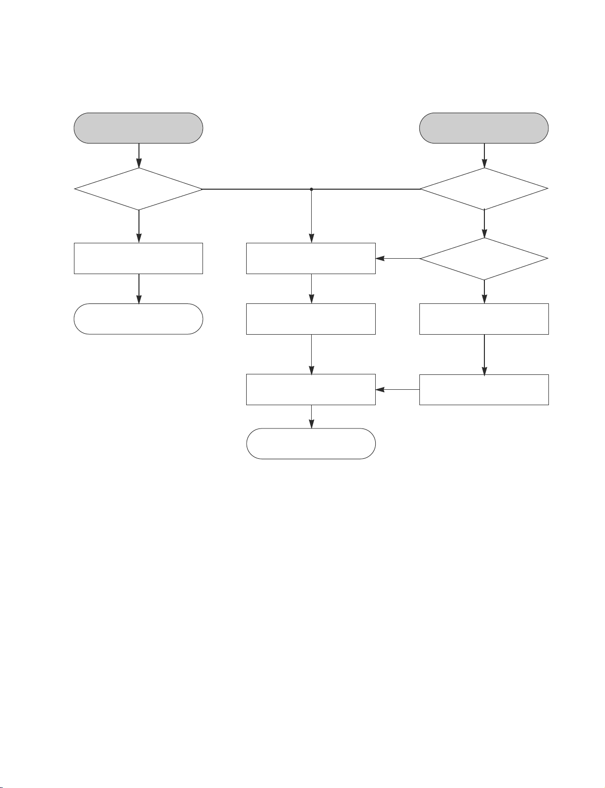
ELECTRICAL TROUBLESHOOTING GUIDE
1. SMPS TROUBLESHOOTING FLOW
No 3.3VA
YES
Is the FR101 normal?
YES
Is the D105/D106/D107/
D108 normal?
YES
Is the Vcc (about 17V)
supplied to IC101 Pin2?
YES
Is the D121 normal?
YES
Is there about 2.5V at the
IC103 Pin1?
YES
NO
NO
NO
NO
NO
Replace the FR101
(Use the same ICW)
Replace the
D105/D106/D107/D108
Check or Replace the IC101
Replace the D121
Replace the IC103
Is the D123 normal?
YES
Is the D125 normal?
YES
Power Line of Main
PCB(DVD) is short
NO
NO
Replace the D123
Replace the D125
3-2
Page 16
ELECTRICAL TROUBLESHOOTING GUIDE
No REG 5.0V
YES
Is the Vcc(=5.6V)
•
•
supplied to Q126
Collector?
YES
Is the Vcc(=12V)
•
•
supplied to Q126
Base?
YES
Check or Replace the Q126
No 12V
YES
Is the Vcc(=14V)
•
•
supplied to Q123
Collector?
NO
NO
NO
Check or Replace the D123
Check the ‘PWR CTL “H”’
signal from μ-com
Check or Replace the D125
YES
Is the Vcc(=12V)
•
•
supplied to Q126
Base?
YES
Check or Replace the Q123
NO
Check the ‘PWR CTL “H”’
signal from μ-com
3-3
Page 17
ELECTRICAL TROUBLESHOOTING GUIDE
2. POWER CHECK FLOW
A. B.
No 5V No 3.3VA.
Is 3.3VA
section working?
YES
Is 5.6V present at
collector of Q126?
YES
Replace Q126. Check FR101 Replace Q121.
NO
No 3.3VA
Is there a DC voltage at
cathode of D105 or D107?
NO
NO
NO
Is 3.3VA
section working?
YES
Is 3.3V
present at emitter
of Q121?
YES
YES
Check D105/D106/D107/
D108 and replace.
YES
Replace IC101.
3-4
Page 18
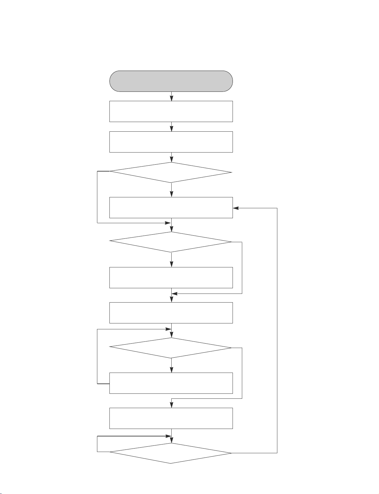
ELECTRICAL TROUBLESHOOTING GUIDE
3. SYSTEM OPERATION FLOW
Power on
1. 8032 initializes SERVO,DSP & RISC registers
2. Write RISC code to SDRAM
3. Reset RISC
Show LOGO
YES
Tray close to closed position
SLED moves to inner position
1. Judge whether have disc and disc type
2. Jump to related disc reading procedure
Recieve OPEN/CLOSE Key?
Tray closed?
NO
SLED at inner side?
NO
YES
YES
NO
1. Execute pressed Key & IR key
2. System operation routine loop
1. Stop playback & open Tray
2. Display tray open message & LOGO
NO
Receive CLOSE Key?
YES
3-5
Page 19
ELECTRICAL TROUBLESHOOTING GUIDE
4. SYSTEM TEST FLOW
TEST
Check the AC
Voltage Power PCBA (110V
or 220V)
YES
Switch on the power PCBA
Is the DC
voltage outputs OK?
(5V, 3.3V, 12V, 5.6V
MOTOR)
YES
Make sure the main PCBA don't
short on VCCs and switch it on.
YES
Is 3.3V
and 1.8V DC outputs normal
on main PCBA?
YES
NO
NO
NO
Replace power PCBA or AC transformer.
Repair or Replace power PCBA
Check the regulators or related diodes.
Connect to PC RS232 cable and
update the FLASH memory code.
Update FLASH
successfully?
YES
A
NO
1. Check 27MHz system clock.
2. Check system reset circuit.
3. Check FLASH R/W enable signal PRD,
RWR.
4. Check RS232 SIGNALS.
5. Check FLASH Memory related circuit.
3-6
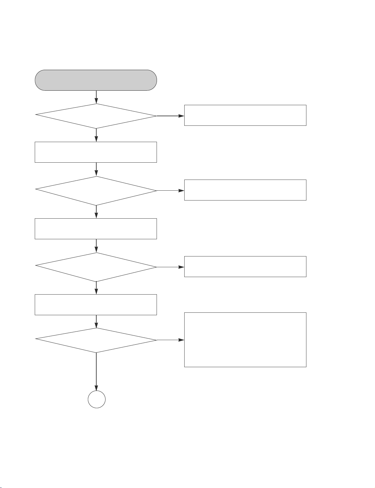
Page 20
ELECTRICAL TROUBLESHOOTING GUIDE
A
RESET or power on.
Show LOGO?
YES
Does
tray move inside
when it is not at closed
position?
NO NO
Flash
memory operates
properly?
YES
SDRAM
NO
works properly?
YES
MT1389S
VIDEO outputs
NO
properly?
YES
Have TV
NO
signal output?
YES
Check AV cable
connection to TV set.
NO
Normal
TROUT & TRIN
NO
signals?
YES
Check connection lines
between FLASH & MT1389S
and the FLASH access time
whether is suitable or not.
Check connection lines
between SDRAM & MT1389S
and the SDRAM is damaged.
Check the related
circuit of MT1389S.
Check the filtering and amp
circuit of TV signal.
Check the load
OPEN & CLOSE switch
B
YES
TRCLOSE & TROPEN
Normal
signal?
YES
Normal
LOAD+ & LOAD-
signal?
YES
Check the cable connection
between main PCBA and loader.
3-7
NO
NO
Check the tray control I/O
pins on MT1389S & AM5890.
Check the tray control
amplifying circuit on Motor driver.
Page 21
ELECTRICAL TROUBLESHOOTING GUIDE
B
Does
the SLED move
to inner side when it is
at outter position?
YES
Do not put in
disc and tray close.
Motor
driver STBY pin
is high?
YES
Is FMSO
DC level higher
than 1.4V?
YES
SL+
and SL- output
properly?
YES
Check the cable
connection with MECHA.
NONO
NO
NO
Check the connection
line of STBY signal.
Check the related
circuit of FMSO.
Check the amp circuit
on motor driver.
Optical Lens
has movements for
searching
focus?
YES
C
Proper
FOSO outputs to
motor driver?
YES
Proper
F+ & F-
outputs?
YES
Check cable connect on
with pick-up head.
3-8
NONO
NO
Check FOSO connection on
MT1389S and motor dirver.
Check the amp circuit
on motor dirver.
Page 22
ELECTRICAL TROUBLESHOOTING GUIDE
C
Laser turns
on when reading
disc?
YES
Put disc in?
YES
Disc ID is
correct?
NO NO
LD01 or LD02
output properly?
YES
Collector
NO
voltage of power transistor
is OK?
YES
Check cable connection
between transistor ouput
and pick-up head.
NO
Laser off
NO
Proper
RFL signal on
NO
MT1389S?
YES
Check the laser power circuit
on MT1389S and connecting
to power transistor.
Check the related circuit on
laser power transistor.
Check the related circuit
on MT1389S RFL signal.
YES
Does
spindle rotate?
YES
D
Check LDO1 & LDO2 signal
NO NO
Proper
DMSO signal on
MT1389S.
YES
SP+ & SP-
NO
output properly?
YES
Check the cable
connection between spindle
and main PCBA.
3-9
Check DMSO related
circuit on MT1389S.
Check the spindle control
amp circuit of motor driver.
Page 23
ELECTRICAL TROUBLESHOOTING GUIDE
D
Focus on OK?
YES
Track on OK?
YES
NO NO
signals on A, B, C, D of
Proper
MT1389S
YES
Check FEO signal
NO
on MT1389S
YES
Check FOSO
signal on MT1389S
NO NO
Normal
TEO Signal on
MT1389S?
YES
Properly
TRSO signal on
NO
MT1389S?
YES
T+ & T- output
NO
properly?
YES
Check connections between
MT1389S and pick-up head.
Check the FOSO connection
on MT1389S and motor driver.
Check the related
circuit on MT1389S
Check the TRSO
connection on MT1389S
and motor dirver.
Check the tracking control
amp circuit on motor driver.
Disc is play?
YES
E
NO
Check cable connection
on pick-up head.
Check RFO & RFLVL
signal waveform.
3-10
Page 24
ELECTRICAL TROUBLESHOOTING GUIDE
E
Normal
Audio output when
disc playback?
YES
Normal
IR.VFD & Front pannel
key functions?
YES
NO
NO
Normal
audio DAC
out?
YES
Check audio filter,
amplify, mute circuit.
Commu-
nications between
IR.VFD Front pannel
key & MT1389S is
normally?
YES
NO
NO
Check the related
circuit of audio DAC.
Check communication
lines on MT1389S.
TEST END
NO
Check the cable
connection on Front pannel.
3-11
Page 25

DETAILS AND WAVEFORMS ON SYSTEM TEST AND DEBUGGIBG
1. SYSTEM 27MHz CLOCK, RESET, FLASH R/W SIGNAL
1) MT1389S main clock is at 27MHz (X601)
1
1
2) MT1389S reset is low active
2
3
4
RESET TIME
FIG 1-1
3.3V
PWR_CTL
2
3
4
IC601
FIG 1-2
3-12
Page 26

3) RS232 waveforn during procedure (Downloading)
5
TXD
6
RXC
FIG 1-3
4) Flash R/W enable signal during download (Downloading)
7
PRD
7
5
6
IC602
8
PWR
8
FIG 1-4
3-13
Page 27

2. SDRAM CLOCK
DCLK = 128MHz, Vp-p=2.2
IC603
9
9
FIG 2-1
3. TRAY OPEN/CLOSE SIGNAL
10
11
12
13
TRIN
TROUT
TRCLOSE
TROPEN
FIG 3-1
IC601
11
10
12
13
3-14
Page 28

4. SLED CONTROL RELATED SIGNAL (NO DISC CONDITION)
15
14
15
16
17
FMSO(1.9V/1.4V/1.1V)
14
STBY(3.3V)
SL+(4.2V/2.8V/1.2V)
SL-(4.2V/2.8V/1.5V)
16
17
FIG 4-1
5. LENS CONTROL RELATED SIGNAL (NO DISC CONDITION)
18
19
20
18
FOSO(1.5V/1.4V/1.3V)
F+(3.2V/2.7V/2.2V)
F-(3.2V/2.7V/2.2V)
20
19
FIG 5-1
3-15
Page 29

6. LASER POWER CONTROL RELATED SIGNAL (NO DISC CONDITION)
IC601
21
22
23
MDI1
(0V/180mV)
LD02
(3.3V/2.3V)
LD01
(3.3V/2.3V)
FIG 6-1
7. DISC TYPE JUDGEMENT WAVEFORM
21
22
23
CN201
24
24
25
26
F+
FE
RFL
FIG 7-1 (DVD)
3-16
IC601
25
26
Page 30

FIG 7-2 (DVD)
F+
FE
RFL
FIG 7-3 (CD)
3-17
F+
FE
RFL
Page 31

8. FOCUS ON WAVEFORM
F+
FE
RFL
FIG 7-4 (CD)
27
28
29
30
IC601
27
FE
28
FOSO
F+
F-
29
30
FIG 8-1 (DVD)
3-18
Page 32

FE
FOSO
F+
F-
FIG 8-2 (CD)
9. SPINDLE CONTROL WAVEFORM (NO DISC CONDITION)
31
32
33
DMSO
(1.4V/1.8V)
SP(3.6V/2.4V)
31
32
SP+
(3.6V/4.8V)
33
FIG 9-1
3-19
Page 33

10. TRACKING CONTROL RELATED SIGNAL (SYSTEM CHECKING)
IC601
34
35
36
37
TE
TRSO
34
T+
T-
FIG 10-1 (DVD)
35
CN201
TE
TRSO
T+
T-
FIG 10-2 (CD)
3-20
36
37
Page 34

11. MT1389S AUDIO OPTICAL AND COAXIAL OUTPUT (SPDIF)
IC601
38
FIG 11-1
38
12. MT1389S VIDEO OUTPUT WAVEFORM
1) Full colorbar signal (CVBS)
FIG 12-1
JK701 2PIN
3-21
Page 35

13. AUDIO OUTPUT FROM MT1389S
FIG 13-1
3-22
Page 36

CONNECTOR PICTURE
1. ALL CONNECTOR PICTURE
3-23
Page 37

2. MAIN BOARD CONNECTOR PICTURE
3-24
Page 38

3. CN201 CONNECTOR PICTURE
CN201 (MD 23PIN)
4. CN202 CONNECTOR PICTURE
CN202 (MD 9PIN)
3-25
Page 39

5. CN601 CONNECTOR PICTURE
CN601 (Front 12PIN)
6. CN602 CONNECTOR PICTURE
3-26
CN602 (POWER 10PIN)
Page 40

7. CN604 CONNECTOR PICTURE
CN604 (USB 4PIN)
8. CN605 CONNECTOR PICTURE
CN605 (KARAOKE 4PIN)
3-27
Page 41

9. CN705 CONNECTOR PICTURE
CN705 (5.1ch 12PIN)
3-28
Page 42

BLOCK DIAGRAMS
JA
CK
1. OVERALL BLOCK DIAGRAM
JACK
3.3V
USB,Karaoke
P
IC604
KA741
OP-AM
A
ADC_DAT
ADC
IC607
CS6340
IC603
64M bit
SDRAM
IC604
3.3VA
FLASH ROM
6M)
(1
ACLK
ABCK
RAMCAS
ROMADD[0:11]
T
ALRCK
ADC_RS
[00:15]
RAMCS1
RAMCS0
RAMRAS
R
RAMBA
IC605
AT24C08A
3.3VA
K
I2CCL
I2CDAT
USBP,USBN
30MHz
ROMDAT
LK
PC
RAMWE
RAMCKE
ROMDATA[0:15]
MEMW
MEMRD
MEMADD[0:19]
3.3VA
1.8VA
EEPROM
L
R
12V
IC702
MC4580
OP-AMP
APWM_R +/=
APWM_L +/=
IC601
MT1389S
RCG_SEL
scart( 16:9)
5V
5V
IC701
S-Video YC
B/
Pb
G/Y
R/Pr
CVBS
SPDIF
27MHz
K
FP CL
FP STB
FP DATA
RF+DSP+5.1ch+karaoke+HDMI Tx + MPEG IC
FFER
VIDEO
BU
RESET
IR RCV
S-VIDEO OPTION
L
COAXIA
OPTICAL
H.H.P.P.D
CK
JA
HDMIHDMI
±
TXC TXC ±
TX[TX[ 0-2-2 ]
Circuit
IRIR
ReceReceiveiver
ToTo F Froront IC IC
DISC
DVD : A,B,C,D,RF
CD : A,B,C,D,E,F,RF
MDI
PICK
MOTOR
SPINDLE
1.8VA
RESET
SO
IC201IC201
A
3.3V
PWR_CTL_H
CDLD,DVDLD,VC20
UP
Pick-up
DP11DP11
M
M
SLED
MOTOR
(FEEDING)
M
MOTOR
LOADING
DECK MECHANISM
TRIN, TROUT
OP(+,-)
FMSO, DMSO,TRSO,FO
STBY, TROPEN, TRCLOSE
TRACK[+,-]
FOCUS[+,-]
SP[+,-]
SLED[+,-]
LOAD[+,-]
e
Voltage
IC201
Motor Driv
AM5890S(5Ch)
5.6VA(M)
5V
ction
dete
BOARD
POWER
50HZ/60Hz
AC 90V~240V
+12V
5.6VA(M)
3.3V
3-29
Page 43

2. POWER (SMPS) BLOCK DIAGRAM
A
12V
OP AMP
LPF
5V
Video Buffer
LPF
Motor Drive IC 1.8V
5.6VA(M)
MPEG
RemoconReceiver
Flash Memory
3.3V
LPF
3.3V
SDRAM
LED Clock,Driver
PWR CTL
RECTIFIER(14V)
RECTIFIER(5.6V)
TRANS
SWITCHING IC
3-30
RECTIFIER(3.3V)
FEED B.
AC100~240V
RECTIFIER
Page 44

3. MPEG & MEMORY BLOCK DIAGRAM
O In
terf
ace
5.5.1C1CH
AL_R
AR_R
OptOption
CENTER
WOOFER
Y_G_OUT
CVBS
R_SY_OUT
B_SC_OUT
VIDVIDEO InO Interfterf aceace
AUDAUDIO
InInterfterface
)
ASPDIF(Optica l
ASPDIF(COAXIAL)
IC605
EEPROM
I2Cdata I2CLK
IC603
SDRAM
64M bit
IC604
: EXCEL, SST, MX
(16 M )
RAMADD[0:11]
RAMCAS -
RAMRAS -
RAMCS1 -
RAMCS0 -
RAMBA
RAMWE -
RAMCKE
RAMDAT[00:15]
PCLK
]
DA[0:15
AD[0:19 ]
RESE T,W R-, CS0 -
FLASH MEMORY
CK
USB
JA
ace
D_MUTE
USBP,US BN
MT1389S
terf
AUDIO In
AR
AL
IC601(M(MPEG + DPEG + DSP + RFSP + RF)
X60X601
27MH27MHz
5V
Y_G_OUT
CVBS
R_SY_OU
B_SC_OUT
IC701
VIDEO
BUFFER
H.P.D
T
TX [0-2 ] , TXC
RESET
IR
POWER,
DIN ,DOUT
IC(IC(IC901)C901)
LED D DRIDRIVE
VIDVIDEO InO Interfterf ace
er
HDMI
IC201
AM5890S(5Ch)
Motor Driv
3-31
Page 45

4. SERVO BLOCK DIAGRAM
L
X601
27MHz
X-TA
IC601
ALPC
MTK1389S
ONE CHIP
DVDPLAYER
P-
RESET
ction
Voltage
dete
OP+, OP-
Y
FMSO,DMSO
FOSO, TRSO
TROPEN,
TRCLOSE,
STB
IC201
,
IOA
MDI1
SEL1
CDLD(LD01),DVDLD(LD02),V20
DVD : A,B,C,D,RF
CD : A,B,C,D,E,F,RF
PICK
TRIN,TROUT
Motor Driver
AM5890S(5Ch)
-
PICK
UP
(IM)
3-32
F+, F-,
T+, T-
SL+, SL-
LOAD+,LOAD
M/D
SP+,S
(DP11)
Page 46

5. VIDEO & HDMI BLOCK DIAGRAM
Y
Pb
Y
RGB_H
16_9_H
V.OUT
B
G
R
CVBS
O
S-VIDE
Pb
Pr
HDMI JACK
Pr
SC
SY
±
±
H.P.D
TX[0- 2] , TXC
Y
Y
CVBS
C
Y_C MIX
Y
C
Y_G
Y(G)
Pb_B_SC
Pr_R_S
Pr(R)
Pb(B)
IC601
Mpeg IC
MT1389S
3-33
Page 47

6. AUDIO BLOCK DIAGRAM
A Out "L"
JACK
A out "R"
2
AMP
IC70
MC4580M
MUTE
S/W
AL_R
AR_R
CENTER
WOOFER
5.1ch
Connector
Option
A_L
A_R
IC601
MT1389S
MPEG
MUTEC
Audio
3-34
8DAC
DIF
COAXl _SP
Coaxial
Serial Stereo
Optical
PDIF
Optical _S
tal Out
Digi
Page 48

CIRCUIT DIAGRAMS
A B C D E F G H I J K L M N O P Q R ST
No Power
D105~D108 is Defective
14VA No Power
D125 is Defective
5.6VA No Power
D123 is Defective
3.3VA No Power
D121 or D122 are Defective
Switching Error
IC101is Defective
Switching Error
IC102,IC103 are Defective
No Power
FR101 is Defective
12V No Power
Q123 is Defective
5.0V No Power
Q126 is Defective
3.3V No Power
Q121 is Defective
1. POWER (SMPS) CIRCUIT DIAGRAM
IMPORTANT SAFETY NOTE :
WHEN SERVICING THIS CHASSIS, UNDER NO CIRCUMSTANCES SHOULD THE ORIGINAL DESIGN BE
MODIFIED OR ALTERED WITHOUT PERMISSION
FROM THE NAD. ALL COMPONENTS SHOULD BE
REPLACED ONLY WITH TYPES IDENTICAL TO
THOSE IN THE ORIGINAL CIRCUIT. SPECIAL COMPONENTS ARE SHADED ON THE SCHEMATIC FOR
EASY IDENTIFICATION. THIS CIRCUIT DIAGRAM MAY
OCCASIONALLY DIFFER FROM THE ACTUAL CIRCUIT USED. THIS WAY, IMPLEMENTATION OF THE
LATEST SAFETY AND PERFORMANCE IMPROVEMENT CHANGES INTO THE SET IS NOT DELAYED
UNTIL THE NEW SERVICE LITERATURE IS PRINTED.
1. Shaded( ) parts are critical for safety. Replace only
with specified part number.
2. Voltages are DC-measured with a digital voltmeter during Play mode.
3-35 3-36
Page 49

2. MPEG CIRCUIT DIAGRAM
3-37 3-38
Page 50

3. SERVO CIRCUIT DIAGRAM
3-39 3-40
Page 51

4. JACK CIRCUIT DIAGRAM
3-41 3-42
Page 52

5. SCART CIRCUIT DIAGRAM (OPTION)
3-43 3-44
Page 53

6. USB CIRCUIT DIAGRAM 7. KEY CIRCUIT DIAGRAM
3-45 3-46
Page 54

8. TIMER CIRCUIT DIAGRAM
3-47 3-48
Page 55

• CIRCUIT VOLTAGE CHART
MODE
PIN NO.
STOP PLAY
IC201(AM5869S)
1 1.392 1.397
2 1.705 1.637
3 1.375 1.436
4 1.393 1.396
5 1.243 1.238
6 0.01 0.01
7 0.02 0.02
8 5.589 5.53
9 0.001 0
10 0.001 0
11 2.729 2.771
12 2.729 2.687
13 2.733 2.686
14 2.733 2.757
15 2.739 2.701
16 2.739 2.725
17 2.734 3.725
18 2.734 1.656
19 5.598 5.55
20 3.277 3.253
21 5.598 5.54
22 0.001 0
23 1.395 1.734
24 3.275 3.251
25 5.574 5.51
26 1.392 1.391
27 1.392 1.391
28 0.019 3.197
29 0 0
30 0 0
IC601(MT1389S)
1 1.728 1.694
2 1.146 1.826
3 0.874 0.883
4 3.259 3.243
5 0.002 0.002
6 0.381 0.381
7 0.391 0.361
8 0.376 0.353
9 0.382 0.346
10 1.741 1.708
11 2.004 2.048
12 2.001 2.045
13 2.003 2.056
14 2.004 2.043
15 0.769 0.439
16 0.769 0.439
17 1.996 1.982
18 1.996 2.241
19 0 0.179
20 0 0.179
21 3.213 2.352
22 3.213 2.352
23 3.237 3.242
24 2.241 2.799
25 0.773 1.367
26 0.002 0.002
27 2.516 2.764
28 1.995 2.003
29 1.389 1.388
30 1.374 1.489
31 1.579 1.364
MODE
PIN NO.
STOP PLAY
32 1.578 1.359
33 2.431 1.824
34 2.593 1.828
35 2.196 1.684
36 1.391 1.834
37 1.391 1.466
38 0.008 0.009
39 1.391 1.391
40 1.388 1.382
41 1.387 1.422
42 0.002 0.001
43 1.859 1.856
44 0.011 0.008
45 0.011 0.008
46 3.281 3.272
47 0.002 0.002
48 0.819 0.794
49 1.859 1.854
50 0.002 0.002
51 0.971 0.864
52 0.971 0.717
53 3.261 0.017
54 3.241 0.022
55 1.848 1.851
56 1.954 2.257
57 1.884 2.054
58 1.947 2.239
59 1.694 1.604
60 1.785 1.783
61 1.816 2.346
62 1.997 1.652
63 0.127 0.125
64 0.012 0.015
65 3.285 3.277
66 3.285 3.276
67 1.393 1.093
68 1.759 1.806
69 1.251 3.043
70 2.245 3.006
71 1.249 3.131
72 0.305 0.712
73 2.466 1.706
74 2.759 1.332
75 0.011 0.013
76 0.011 0.013
77 2.079 1.895
78 0.011 0.012
79 1.369 1.523
80 1.705 1.803
81 0.002 0.002
82 0.585 0.854
83 0.971 0.956
84 1.561 1.616
85 1.547 1.469
86 1.683 0.974
87 0.021 0.024
88 1.171 1.127
89 1.368 1.117
90 0.002 0.002
91 0.025 0.024
92 1.998 1.846
93 1.876 1.828
94 3.254 3.257
MODE
PIN NO.
100 0.128 0.127
101 3.276 3.275
102 3.276 0
103 3.276 3.277
104 3.276 3.278
105 3.251 3.278
106 3.264 3.276
107 0.023 0.024
108 3.295 3.293
109 2.991 3.011
110 0.021 0.024
111 2.293 1.965
112 0.024 0.081
113 0.972 0.659
114 0.859 0.643
115 0.982 0.648
116 1.032 0.667
117 1.507 0.945
118 3.286 3.277
119 1.129 0.876
120 1.119 0.813
121 1.251 1.317
122 0.814 0.547
123 1.731 1.323
124 1.686 1.234
125 1.414 1.245
126 1.229 0.751
127 1.175 0.727
128 1.095 0.775
129 1.326 0.739
130 0.055 0.046
131 3.286 3.276
132 2.296 1.916
133 3.001 2.834
134 3.159 3.093
135 3.065 3.066
136 2.815 2.669
137 1.473 1.532
138 1.667 1.572
139 0.038 0.093
140 0.041 0.612
141 2.061 1.647
142 1.842 1.825
143 2.304 1.994
144 1.372 1.534
145 3.286 3.277
146 1.479 1.431
147 3.261 3.276
148 0.002 0.002
149 0.032 0.039
150 0.079 0.081
151 0.051 0.054
152 1.444 1.529
153 1.489 1.561
154 1.459 1.521
155 1.516 1.503
156 3.288 3.275
157 3.127 3.125
STOP PLAY
95 3.256 3.252
96 3.286 3.276
97 0.021 0.078
98 3.227 3.232
99 3.159 3.151
MODE
PIN NO.
158 3.266 3.258
159 4.82 4.82
160 1.842 1.829
161 4.84 4.84
162 0.021 0.017
163 0.002 0.002
164 1.331 1.33
165 3.099 3.086
166 3.099 3.086
167 0.345 0.208
168 0.001 0.001
169 0.001 0.001
170 0.001 0.001
171 0.003 0.004
172 1.842 1.831
173 0.002 0.001
174 0.002 0.002
175 0.001 0.001
176 0.002 0.003
177 0.002 0.002
178 1.845 1.832
179 0.002 0.002
180 0.002 0.002
181 0.002 0.002
182 0.637 0.032
183 0.701 0.034
184 0.003 0.003
185 0.496 0.127
186 3.251 3.237
187 2.614 2.567
188 0.003 0.002
189 0.676 0.659
190 3.251 3.238
191 0.498 0.281
192 0.002 0.002
193 1.212 1.207
194 1.289 1.203
195 3.251 3.239
196 0.016 0.018
197 0.016 0.018
198 0.024 0.022
199 0.024 0.022
200 0.024 0.023
201 0.128 3.248
202 0.027 0.023
203 0.024 1.523
204 0.023 1.608
205 0.023 1.635
206 2.915 1.321
207 3.266 3.256
208 0.023 0.024
209 0.023 0.024
210 0.018 0.021
211 0.019 3.218
212 1.831 1.829
213 0 0
214 2.945 2.936
215 1.539 1.533
216 3.241 3.251
217 1.892 1.698
218 0.002 0.002
219 0.002 0.002
220 0.002 0.002
STOP PLAY
MODE
PIN NO.
221 1.617 1.615
222 2.261 2.249
223 1.617 1.613
224 0 0
225 1.619 1.611
226 1.617 1.611
227 1.616 1.61
228 3.286 3.249
229 3.286 3.248
230 1.618 1.614
231 1.616 1.611
232 0.003 0.003
233 3.286 3.249
234 1.841 1.827
235 0.002 0.002
236 0.003 0.003
237 1.841 1.827
238 0.871 0.868
239 0.887 0.868
240 1.071 0.864
241 1.035 0.822
242 0.002 0.002
243 3.202 3.179
244 1.636 1.641
245 0.321 1.549
246 1.986 1.543
247 0.221 1.517
248 3.259 3.244
249 0.002 0.002
250 3.259 2.243
251 0.691 1.711
252 1.375 1.366
253 3.236 1.424
254 1.368 1.788
255 0.002 0.002
256 1.723 1.718
STOP PLAY
IC602(ES29LV160ET)
1 1.392 0.118
2 2.326 0.339
3 0.883 3.065
4 1.468 0.338
5 1.247 3.163
6 0.299 0.619
7 2.478 1.645
8 2.767 1.648
9 0.012 0.014
10 0.021 0.014
11 3.274 3.242
12 3.266 3.239
13 3.268 3.244
14 3.268 3.244
15 1.204 0.776
16 0.014 0.015
17 0.102 3.085
18 2.006 1.765
19 1.114 1.354
20 2.285 2.265
21 1.698 2.084
22 1.953 2.118
23 1.891 1.945
24 1.964 2.175
25 2.087 1.869
26 0.012 0.014
MODE
PIN NO.
27 0.002 0.001
28 0.012 0.013
29 1.376 1.561
30 0.528 0.202
31 1.706 1.766
32 0.436 0.775
33 0.961 1.188
34 0.441 0.587
35 0.588 1.134
36 0.365 0.729
37 3.267 3.241
38 1.383 1.442
39 0.432 1.291
40 1.505 1.536
41 0.413 0.847
42 1.637 1.527
43 0.447 1.028
44 1.339 1.142
45 2.012 1.846
46 0.001 0.001
47 0.001 0.001
48 0.014 0.026
STOP PLAY
IC603(HY57V64)
1 3.281 3.239
2 1.264 1.141
3 3.281 3.239
4 1.154 1.055
5 1.145 1.077
6 0.002 0
7 1.504 1.021
8 1.005 1.241
9 3.281 3.241
10 1.003 1.069
11 0.843 0.633
12 0.002 0
13 0.968 0.782
14 3.284 3.241
15 2.316 1.389
16 3.181 3.001
17 3.022 2.748
18 3.098 2.934
19 2.856 3.239
20 1.485 1.233
21 1.679 1.229
22 0.039 0.097
23 0.411 0.715
24 2.076 1.238
25 2.318 1.775
26 1.384 1.507
27 3.279 3.241
28 0.002 0.001
29 1.511 1.381
30 1.543 1.649
31 1.651 1.539
32 1.705 1.508
33 0.054 0.084
34 0.087 0.083
35 0.033 0.036
36 0 0
37 3.271 3.246
38 1.518 1.462
39 2.316 1.538
40 0 0
MODE
PIN NO.
41 0.002 0.001
42 1.339 0.796
43 3.278 3.267
44 1.117 0.885
45 1.217 1.009
46 0.002 0
47 1.231 1.144
48 1.473 0.745
49 3.279 3.267
50 1.742 1.127
51 1.786 1.281
52 0.002 0.001
53 0.828 1.051
54 0.002 0.001
STOP PLAY
IC606(S524C80D80-SCB1)
1 0.002 0
2 0.002 0
3 0.002 0
4 0.002 0
5 3.285 3.252
6 3.285 3.251
7 0.002 0
8 3.289 3.252
IC607(CS5340)
1 3.283 3.247
2 0.026 0.024
3 3.287 3.251
4 2.929 2.909
5 0.001 0.001
6 4.911 4.88
7 0.022 0.025
8 0.022 0.025
9 3.286 3.253
10 2.448 2.439
11 2.448 2.437
12 2.442 2.434
13 4.89 4.89
14 0.002 0
15 0.346 0.346
16 3.283 3.246
IC701(MM1692XVBE)
1 4.859 4.83
2 2.284 2.276
3 2.436 2.427
4 1.851 1.786
5 4.861 4.84
6 1.847 1.691
7 0.014 0.013
8 2.282 2.271
9 2.255 2.271
10 0.003 0.003
11 2.245 2.252
12 2.229 2.239
13 1.961 1.729
14 1.945 1.727
15 1.901 1.701
16 2.231 2.242
IC703(MC4580)
1 5.57 5.54
2 5.57 5.54
3 5.57 5.54
4 0.001 0.001
5 5.57 5.54
MODE
PIN NO.
STOP PLAY
6 5.57 5.54
7 5.57 5.54
8 12.21 12.13
Q201
Emitter 3.297 3.266
Collector 0.384 0.034
Base 3.237 3.221
Q202
Emitter 3.301 3.039
Collector 0.385 2.328
Base 3.242 2.305
Q205
Emitter 0 0.002
Collector 0.008 4.887
Base 0.651 0.019
Q206
Emitter 0 0.001
Collector 0 0.179
Base 3.234 0.022
Q207
Emitter 0 0.001
Collector 0 0.001
Base 0.008 4.839
Q208
Emitter 1.751 1.705
Collector 1.885 1.886
Base 2.482 2.461
Q601
Drain 3.296 3.271
Gate 3.107 3.093
Source 4.912 4.912
Q702
Emitter 0.001 0.001
Collector 0.005 0.002
Base 0.716 0.667
Q703
Emitter 3.269 3.257
Collector 3.239 3.115
Base 2.558 3.247
Q705
Emitter 0.001 0.001
Collector 0.005 0.003
Base 0.726 0.671
Q706
Emitter 0.002 0.002
Collector 0.082 0.083
Base 0.729 0.727
Q707
Emitter 0.001 0.001
Collector 0.085 0.081
Base 0.728 0.728
Q708
Emitter 0.001 0.001
Collector 0.034 0.035
Base 0.728 0.727
Q709
Emitter 2.271 2.254
Collector 4.86 4.86
Base 2.921 2.902
3-49 3-50
Page 56

LOCATION SPEC
C642 33μ F/16V 1.858 0.002
C666 100μ F/6.3V 3.244 0.003
C6C1 10μ F/16V 12.251 0
C6C2 10μ F/16V 11.556 0
C6C6 10μ F/16V 3.257 0.001
C6C9 220μ F/16V 3.259 0.001
C6E0 47μ F/6.3V 2.758 0.001
C6E1 10μ F/16V 1.372 0.002
C6E2 47μ F/6.3V 1.396 0.002
C6E3 220μ F/6.3V 3.239 0.003
C6E4 220μ F/6.3V 3.268 0
C6E5 10μ F/16V 3.261 0.002
C6E6 100μ F/6.3V 3.165 0.003
C6E7 47μ F/6.3V 2.012 0.002
C6E8 10μ F/16V 1.852 0.002
C6E9 10μ F/16V 3.227 0.002
C202 220μ F/6.3V 3.257 0.001
C205 47μ F/6.3V 3.252 3.209
C206 47μ F/6.3V 3.252 2.254
C217 100μ F/6.3V 4.884 0.002
C220 220μ F/16V 5.515 0.016
C240 220μ F/6.3V 1.888 0.001
C242 10μ F/16V 3.266 0.002
C703 22μ F/16V 2.438 0.002
C704 47μ F/6.3V 4.859 0.002
C706 10μ F/16V 4.817 0.002
C728 47μ F/16V 12.256 0.145
C730 22μ F/16V 5.595 1.609
C731 47μ F/16V 5.599 0.002
C732 22μ F/16V 5.595 1.611
C734 22μ F/16V 5.595 0.006
C735 22μ F/16V 5.595 0.006
PLAY
+
-
3-51 3-52
Page 57

PRINTED CIRCUIT BOARD DIAGRAMS
1. MAIN P.C.BOARD
(TOP VIEW) (BOTTOM VIEW)
3-53 3-54
Page 58

2. POWER (SMPS) P.C.BOARD
(TOP VIEW) (BOTTOM VIEW)
3. KEY P.C.BOARD
(TOP VIEW)
(BOTTOM VIEW) (BOTTOM VIEW)
4. TIMER P.C.BOARD
(TOP VIEW)
3-55 3-56
Page 59

5. SCART P.C.BOARD (OPTION)
(TOP VIEW) (BOTTOM VIEW)
6. USB P.C.BOARD
(TOP VIEW) (BOTTOM VIEW)
3-57 3-58
Page 60

SECTION 4
MECHANISM (DP-12V)
CONTENTS
DECK MECHANISM PARTS LOCATIONS
• Top View......................................................................................................................................4-2
• Top View(without Tray Disc) .....................................................................................................4-2
• Bottom View ...............................................................................................................................4-2
DECK MECHANISM DISASSEMBLY
1. Main Base ....................................................................................................................4-3
1-1. Clamp Assembly Disc .........................................................................................................4-3
1-1-1. Plate Clamp ..............................................................................................................4-3
1-1-2. Magnet Clamp ..........................................................................................................4-3
1-1-3. Clamp Upper ............................................................................................................4-3
2. Tray Disc ......................................................................................................................4-3
3. Base Assembly Sled...................................................................................................4-4
3-1. Gear Feed...........................................................................................................................4-4
3-2. Gear Middle ........................................................................................................................4-4
3-3. Gear Rack...........................................................................................................................4-4
4. Rubber Rear.................................................................................................................4-4
5. Frame Assembly Up/Down.........................................................................................4-5
6. Belt Loading ................................................................................................................4-5
7. Gear Pulley ..................................................................................................................4-5
8. Gear Loading ...............................................................................................................4-5
9. Guide Up/Down ...........................................................................................................4-5
10. PWB Assembly Loading...........................................................................................4-5
11. Base Main...................................................................................................................4-5
EXPLODED VIEW
1. Deck Mechanism Exploded View ..............................................................................4-7
4-1
Page 61

DECK MECHANISM PARTS LOCATION
• TOP VIEW (WITHOUT TRAY)
• TOP VIEW (WITH TRAY)
Procedure
Starting No.
1 Main Base 4-1
12
1, 2 3 Plate Clamp 4-1
1, 2, 3 4 Magnet Clamp 4-1
1, 2, 3, 4 5 Clamp Upper 4-1
1 6 Tray Disc 4-2
1, 6 7 Base Assembly Sled 4-3
1, 2, 6 8 Gear Feed 1 Connector 4-3
1, 2, 6, 8 9 Gear Middle
1, 2, 6, 8,
9
1, 2, 7 11 Rubber Rear 4-3
1, 2, 7 12
1, 2 13 Belt Loading 1 Locking Tab 4-4
1, 2 ,13 14 Gear Pulley 4-4
1, 2, 13, 14 15 Gear Loading 1 Locking Tab 4-4
1, 2, 7, 12,
13, 14
1, 2, 13 17 PWB Assembly
1, 2, 7, 12,
13, 14, 15, 18 Base Main 2 Locking Tabs 4-4
16, 17
10 Gear Rack 1 Screw 4-3
16 Guide Up/Down 4-4
Parts Fixing Type
Clamp Assembly
Disc
Frame Assembly
Up/Down
Loading
4 Screws,
1 Locking Tabs
1 Screw Bottom 4-4
1 Locking Tab
1 Hook
2 Screw
Disass Fig-
embly ure
4-1
Bottom 4-4
• BOTTOM VIEW
Note
When reassembling, perform the procedure in
reverse order.
The “Bottom” on Disassembly column of above
Table indicates the part should be disassembled
at the Bottom side.
4-2
Page 62

DECK MECHANISM DISASSEMBLY
MAIN BASE
PLATE CLAMP
MAGNET CLAMP
CLAMP UPPER
HOLDER
BASE MAIN
(Fig. A)
DISC CLAMP ASSEMBLY
TRAY DISC
BASE MAIN
LEVER
FIG. 4-1 FIG. 4-2
1. MAIN BASE (FIG. 4-1)
1-1. Clamp Assembly Disc
1) Place the Clamp Assembly Disc as Fig. (A)
2) Lift up the Clamp Assembly Disc in direction of
arrow(A).
3) Separate the Clamp Assembly Disc from the
Holder Clamp.
1-1-1. Plate Clamp
1) Turn the Plate Clamp to counterclockwise
1-1-2. Magnet Clamp
1-1-3. Clamp Upper
direction and then lift up the Plate Clamp.
BASE MAIN
BOTTOM SIDE VIEW
2. TRAY DISC (FIG. 4-2)
1) Insert and push a Driver in the emergency eject
hole(A) at the right side, or put the Driver on the
Lever(B) of the Gear Emergency and pull the
Lever(B) in direction of arrow so that the Tray
Disc is ejected about 15~20mm.
2) Pull the Tray Disc until it is separated from the
Base Main completely.
4-3
Page 63

RUBBER DAMPER
(S2)
RUBBER D
Distinguish upper and
lower sides
(Assemble with care)
AMPER
(S2)
GENERAL PICK UP ASSEMBLY
GEAR RACK
SPINDLE MOTOR ASSEMBLY
(S2)
(S2)
BASE PU
RUBBER DAMPER
Distinguish upper and
lower sides
(Assemble with care)
FIG. 4-3
3. BASE ASSEMBLY SLED (FIG. 4-3)
1) Release 4 Screw (S2).
2) Disconnect the FFC Connector (C1)
3-1. Gear Feed
3-2. Gear Middle
3-3. Gear Rack
1) Release the Scerw (S3)
4. RUBBER REAR (FIG. 4-3)
4-4
Page 64

SCREW INSERTION
TORGUE CONTROL
(800gf DOWN)
GEAR PULLEY
(L4)
BELT LOADING
GEAR LOADING
PWB ASSEMBLY LOADING
BASE MAIN
GUIDE UP/DOWN
BASE MAIN
(H1)
(C2)
(S5)
(A)
(B)
GUIDE UP/DOWN
FIG. 4-4
GUIDE UP/DOWN
(A)
(L5)
FIG. (A)
(B)
(C)
FIG. (C)
5. FRAME ASSEMBLY UP/DOWN (FIG. 4-4)
Note
Put the Base Main face down (Bottom Side)
1) Release the screw (S4)
2) Unlock the Locking Tab (L3) in direction of arrow
and then lift up the Frame Assembly Up/Down to
separate it from the Base Main.
Note
• When reassembling move the Guide Up/Down in
direction of arrow(C) until it is positioned as
Fig.(C).
• When reassembling insert (A) portion of the
Frame Assembly Up/Down in the (B) portion of
the Guide Up/Down as Fig.(B)
6. BELT LOADING(FIG. 4-4)
Note
Put the Base Main on original position(Top Side)
7. GEAR PULLEY (FIG. 4-4)
1) Unlock the Locking Tab(L4) in direction of
arrow(B) and then separate the Gear Pulley from
the Base Main
(A)
(B)
GUIDE UP/DOWN
UP/DOWN FRAME ASSEMBLY
FIG. (B)
8. GEAR LOADING (FIG. 4-4)
9. GUIDE UP/DOWN (FIG. 4-4)
1) Move the Guide Up/Down in direction of
arrow(A) as Fig.(A)
2) Push the Locking Tab(L5) down and then lift up
the Guide Up/Down to separate it from the Base
Main.
Note
When reassembling place the Guide Up/Down as
Fig.(C) and move it in direction arrow(B) until it is
locked by the Locking Tab(L5). And confirm the Guide
Up/Down as Fig.(A)
10. PWB ASSEMBLY LOADING (FIG. 4-4)
Note
Put the Base Main face down(Bottom Side)
1) Release 1 Screws(S5)
2) Unlock the Loading Motor (C2) from the Hook
(H1) on the Base Main.
3) Unlock 2 Locking Tabs(L6) and separate the
PWB Assembly Loading from the Base Main.
11. BASE MAIN (FIG. 4-4)
4-5
Page 65

MEMO
4-6
Page 66

EXPLODED VIEW
1. DECK MECHANISM EXPLODED VIEW
DP-12V
A26
026
A02
017
013
015
435
439
015B
015A
001
A01
002
003
018
014
020
016
010
440
442
A03
012
442
012
442
037
012
019
4-7 4-8
Page 67

MEMO MEMO
4-9 4-10
Page 68

NOTES)
)
If you want to purchase
Flash memory, you must order
" IC602A "
NOTES)
Warning
Parts that are shaded are critical with
respect to risk of fire or electrical
shock.
SECTION REPLACEMENT PARTS LIST
MODEL :5T517C/T517CT(NAD,SWEDEN
RUN DATE : 17-JUNE-08
SALLOCA. NO. PART NO. DESCRIPTION SPECIFICATION REMARKS
*** INDIVIDUAL PARTS ***
250 MBN42830502 Case PRESS PCM 0.825 DV302H-NE PRES T517C
250 MBN42830501 Case PRESS PCM 0.825 DV302H-NE PRES T517CT
275 MGJ37320101 Plate,Ground PRESS STS 301 0.2mm MDD102 USB
276 MEG40359801 Holder MOLD HIPS 60HR DVD DV300 MOLD
283 3580R-T229C Door,Case MOLD ABS HF-380 DVD DVN156 (GR T517C
283 3580R-T229D Door,Case MOLD ABS HF-380 DVD DVN156 (TI T517CT
300 6410RCHP04A Power Cord Assembly HIT-101/H03VVH2-F/2X0.75MM2/70
460 1SZZR-0098H Screw,Customized - + 3MM 8MM MSWR FZW SIN JIN T517C
463 1SZZR-0098G Screw,Customized 1SZZR-0098G FH + 3MM 8MM MSWR T517CT
461 1SZZR-0098L Screw,Customized - + 3MM 16MM MSWR NI PLT SIN
462 1SZZR-0098J Screw,Customized 1SZZ0098J BH + 3MM 6.5MM MSWR
463 1SZZR-0098G Screw,Customized 1SZZR-0098G FH + 3MM 8MM MSWR
465 1SZZR-0097N Screw,Customized - + 3MM 8MM MSWR FZB SIN JIN
470 353-022S Screw,Customized BZN BK (CR +3) SPECIAL + 3MM 6
801 AFN52750438 Manual Assembly,Owners DVD DV302H-E.BSWENNK/T ASS'Y
802 MAY46749440 Box,Master BOX SW3 519 136 299 2 COLOR DV T517C
802 MAY46749442 Box,Master BOX SW3 519 136 299 2 COLOR DV T517CT
803 MFZ47272604 Packing CUTTING EPS DVD DV300-N_NAD 91
804 3880SCS001G Bag CUTTING HDPE 100 100 0.05 BAG NSP
808 534-008C Dry Cell Battery AAA(R03) 1PAIR 1.5V 50MAH AAA
900 6711R2N124D Remote Controller Assembly NAD DV302H-NE 08 DVD-P NAD
*** Accessory Assembly ***
810 6851R-0074B Accessory Assembly VCR LGEIN 1WAY YELLOW 1.2M + 2
811 6850R-PAA2F Cable,Assembly RCA PLUG RCA PLUG 1.2M 1P YELL
812 6850R-PBA2H Cable,Assembly RCA PLUG RCA PLUG 1.2M 2P RED/
*** Deck Assembly,DVD(MD) ***
A26 EAZ38311314 Deck Assembly,DVD DECK/MECHA DP-12V player (IN) NSP
A02 AAN34279702 Base Assembly DP-12 Loading 430mm
013 4400R-0010A Belt MOLD RUBBER DVD DP-9 OTHER LOA
014 4470R-0154A Gear COMPLEX DVD DECK/MECHA DP8 PUL
015 4681R-A015C Motor Assembly,DC DVD DP-9 loading
017 4470R-0176A Gear MOLD POM DVD DP-9 LOADING MO
435 1SZZR-0011A Screw,Customized MACHINE
439 1SZZR-0075A Screw,Customized - + 1.7MM 10MM SWRCH FZW SIN
440 1SZZH-1007B Screw,Customized + D2.0 6MM SWRCH16A/ZNBK 4MM 1
015A 4680R-E008A Motor,DC RF-300EA-1D390(80MM) 2V 90MA 2 NSP
015A EAU36590901 Motor,DC FC08I20TLG-1 2V 100MA 0A 1.37K NSP
015A EAU43506801 Motor,DC JQ24-35H390 2V 90A 28A 0RPM 0R NSP
015B 4560R-0008A Pulley MOLD POM DVD MD MOLD -
016 EBR34880104 PCB Assembly DP-12 FEEDING/LOADING -430mm
018 MEA32088501 Guide MOLD POM(LUCEL N109-LD) DVD PO
020 MAM38555601 Base MOLD ABS XR-401 DP-13 MOLD mai NSP
A03 AAN34281204 Base Assembly DP-12V Sled 430mm
010 EAD34861101 Cable,FFC AT10023270D01 270MM 1.00MM 23P
012 MCQ38556902 Damper EXTRUSION BUTYL RUBBER DECK/ME
019 MDQ38556002 Frame MOLD ABS XR-401 DP-12 MOLD up
037 EAZ40060202 Pick Up Assembly CMS-S77RFV(1) CMS-S77RFV(1) IM
Not Service Part
1-5
Page 69

SALLOCA. NO. PART NO. DESCRIPTION SPECIFICATION REMARKS
r
(
442 FAB30124101 Screw,Taptite 1szzr-0064 PWH + B 2.6MM 7MM S
A01 ACA34280801 Clamp Assembly DECK/MECHA DP-12/13 ferrite ty
001 MGJ38556601 Plate PRESS SECC 0.8 dp-13 PRESS upp NSP
002 RAB30611501 Magnet,Ferrite FERRITE 50G NSP
003 MBU38556801 Clamp MOLD POM DECK/MECHA dp-13 MOLD NSP
026 MJS31956302 Tray MOLD ABS XR-401 DVD dp-12 MOLD
*** PCB Assembly,Powe
A47 EBR42200724 PCB Assembly,Power DV300'S SMPS IN WIDE NAD Total
BC101 636-004C Filter,Bead BFS3550R2FD8 70OHM 9X3.5X7.5MM
C101 624-088F Capacitor,Film,DIP PCX2 335 M9663 100nF 10% 275V
C101 624-088J Capacitor,Film,Box ECQU2A104ML 0.1uF 20% 250V MPE ALTERNATE
C101 624-088L Capacitor,Film,DIP 435D UL 250V/ VDE 275V 104 K 1 ALTERNATE
C101 624-088N Capacitor,Film,Box MPX104K2YL UL 250V/ VDE 275V 0 ALTERNATE
C103 0CZZR00011B Capacitor,Unclassified SAMYOUNG,SAMWHA,G-LUXON E-CAP
C104 0CZZR00011B Capacitor,Unclassified SAMYOUNG,SAMWHA,G-LUXON E-CAP
C105 0CQ1031Y519 Capacitor,Film,DIP 230S 2J 103 K 10nF 10% 630V MP
C106 624-087S Capacitor,Unclassified 47PF D 1KV 10% TR B(Y5P)
C108 0CN1040K948 Capacitor,Ceramic,Axial CH UP050 F104Z-A-B Z 100nF -20
C109 624-085D Capacitor,AL,Radial KME5.0TP50VB47M 47uF 20% 50V 1
C111 0CG2220U630 Capacitor,Ceramic,Radial SDE2G222M12BW1 2200pF 20% 400V
C113 0CQ1521N409 Capacitor,Film,DIP HPE 2A 152J TP 1.5nF 5% 100V P
C114 0CQ4721N409 Capacitor,Film,DIP 310M 2A 472 J 4.7nF 5% 100V PE
C121 0CE108BD630 Capacitor,AL,Radial RUS1A102MIS 1000uF 20% 10V 626
C122 0CE3376D638 Capacitor,AL,Radial SMS5.0TP10VB330M 330uF 20% 10V
C123 0CE108EF630 Capacitor,AL,Radial KMG5.0MC16VB1000M 1000uF 20% 1
C123 0CE108BF630 Capacitor,AL,Radial KME4.0CC16VB1000M 1000uF 20% 1 ALTERNATE
C124 0CE3376D638 Capacitor,AL,Radial SMS5.0TP10VB330M 330uF 20% 10V
C126 624-085D Capacitor,AL,Radial KME5.0TP50VB47M 47uF 20% 50V 1
C128 0CQ1042K409 Capacitor,Film,DIP 310M 1H 104 J 100nF 5% 50V PE
C153 0CE4754K638 Capacitor,AL,Radial ESS475M050T1A5B07G 4.7uF 20% 5
C154 0CE1054K638 Capacitor,AL,Radial ESS105M050T1A5B07G 1uF 20% 50V
C155 0CE1076F638 Capacitor,AL,Radial SMS5.0TP16VB100M 100uF 20% 16V
C156 0CN223AK948 Capacitor,Ceramic,Axial CH UP050 F223Z-A-B Z 22nF -20T
C157 0CN223AK948 Capacitor,Ceramic,Axial CH UP050 F223Z-A-B Z 22nF -20T
D101 0DRRE00163A Diode,Rectifier 1F7 1KV 1.3V 5UA 25A 500NSEC R
D101 0DD221009AA Diode,Rectifier ERA22-10 1KV 1.5V 10UA 10A 400 ALTERNATE
D101 0DR400709AA Diode,Rectifier 10SP07U(SUF4007SP) 1KV 1.7V 5U ALTERNATE
D104 0DR104009BA Diode,Rectifier RL104F 400V 1.3V 5UA 30A 150NS
D104 0DRGF00239A Diode,Rectifier FR104E 400V 1.3V 5UA 30A 150NS
D104 0DD010009AC Diode,Rectifier EU01W(R-FORM) 400V 2.5V 10UA 1
D105 0DRRE00203A Diode,Rectifier 1A7 600V 1.1V 5UA 25A - R1 TP
D105 0DRGF00309A Diode,Rectifier 1A5 600V 1.1V 1A 25A 1NSEC R1
D106 0DRRE00203A Diode,Rectifier 1A7 600V 1.1V 5UA 25A - R1 TP
D106 0DRGF00309A Diode,Rectifier 1A5 600V 1.1V 1A 25A 1NSEC R1
D107 0DRRE00203A Diode,Rectifier 1A7 600V 1.1V 5UA 25A - R1 TP
D107 0DRGF00309A Diode,Rectifier 1A5 600V 1.1V 1A 25A 1NSEC R1
D108 0DRRE00203A Diode,Rectifier 1A7 600V 1.1V 5UA 25A - R1 TP
D108 0DRGF00309A Diode,Rectifier 1A5 600V 1.1V 1A 25A 1NSEC R1
D121 0DR158220AA Diode,Schottky 1N5822 950MV 40V 3A 1NSEC 250p
D123 0DR202000AB Diode,Rectifier HER202 100V 1V 5UA 60A 50NSEC
D123 0DSTW00070A Diode,Rectifier HER202-TSC 100V 1V 5UA 60A 50N ALTERNATE
D125 0DR104009BA Diode,Rectifier RL104F 400V 1.3V 5UA 30A 150NS
D125 0DRGF00239A Diode,Rectifier FR104E 400V 1.3V 5UA 30A 150NS
D125 0DD010009AC Diode,Rectifier EU01W(R-FORM) 400V 2.5V 10UA 1
D151 0DS141489BB Diode,Switching 1N4148(26MM) 1V 100V 150MA 500
D151 0DD133009AA Diode,Switching 1SS133 1.2V 90V 400MA 600MA 4N ALTERNATE
FR101 0RM0221K634 Resistor,Cement ICW02M22R20J 2.2OHM 5% 2W 27X1
POWER) ***
2-5
Page 70

SALLOCA. NO. PART NO. DESCRIPTION SPECIFICATION REMARKS
y
(
IC101 EAN34789801 IC,PWM Controller STR-A6259H 12.9V TO 15.7V 10V
IC102 6500RDB011B Sensor,Position K1010B 5V DIP BK 4P 4PIN PHOTO
IC102 657-063A Sensor,Position LTV-817B 5V DIP BK 2P PHOTO CO ALTERNATE
IC103 0IPMGUC004B IC,LDO Voltage Regulator TL431 MAX12V 3.3V 600MW TO92 T
IC103 0IKE431000A IC,Voltage Regulator KIA431 36V 36V 700MW TO92 TP 3 ALTERNATE
IC103 0ISS431000A IC,Voltage Regulator KA431AZ 2.495TO36V 36V 770MW T ALTERNATE
L101 EAM34728301 Filter,Line Noise LFU1116H2-01300 35MH 19X18X16M
L121 633-088G Coil,Choke 22KS 22uH - - 8X17MM LEAD - G
L121 6200J000147 Filter,Unclassified LPL0813T-220K ABCO TAPING
L121 6140R-C011A Coil,RF 6140R-C011A 22uH - - 8X17MM LE
L122 633-088G Coil,Choke 22KS 22uH - - 8X17MM LEAD - G
L122 6200J000147 Filter,Unclassified LPL0813T-220K ABCO TAPING
L122 6140R-C011A Coil,RF 6140R-C011A 22uH - - 8X17MM LE
P101 6631R-E078Q Harness,Single GIL-S10/9073 10ST 60mm GIL-S-1
PW101 6630V90108A Connector,Wafer JE202-2L-03 2P 3.96MM 1R ANGLE
Q121 0TR127109AA TR,Bipolar KTA1271Y PNP -5V -35V -30V -0.
Q122 0TR319809AC Transistor Assembly KTC3198 KTC3198 TP KEC - - -BL
Q122 0TR319909AF TR,Bipolar KTC3199-BL NPN 5V 50V 50V 150M ALTERNATE
Q122 0TR534309BA TR,Bipolar 2SC5343L NPN 5V 60V 50V 150MA ALTERNATE
Q123 0TR320309AA TR,Bipolar KTC3203 NPN 5V 35V 30V 800MA 1
Q123 0TR534409AA TR,Bipolar 2SC5344Y NPN 5V 35V 30V 800MA ALTERNATE
Q124 0TR220309AF TR,Bipolar SRA2203 PNP -40V - -50V -0.1A
Q124 0TR103009AF TR,Bipolar KRA103M(KRA2203) PNP -40V 0V - ALTERNATE
Q126 0TR320509AB Transistor Assembly KTC3205-Y(KTC2236A) KTC3205-Y(
Q126 0TR232809AB TR,Bipolar KSC2328A-Y NPN 5V 30V 30V 2A 1 ALTERNATE
Q126 0TR186209AB TR,Bipolar STD1862LY-AT NPN 5V 30V 30V 2A ALTERNATE
R102 0RS0101K619 Resistor,Metal Oxide Film RSD02R1J1R00 1OHM 5% 2W 12.0X4
R103 0RS5602K619 Resistor,Metal Oxide Film SML02R0J56K0 56KOHM 5% 2W 8.6X
R105 0RD0472F608 Resistor,Carbon Film RD-96S1J47R0 47OHM 5% 1/6W 3.2
R121 0RD1001F608 Resistor,Carbon Film RD-96S1J1K00 1KOHM 5% 1/6W 3.2
R122 0RD5600F608 Resistor,Carbon Film RD-96S1J560R 560OHM 5% 1/6W 3.
R123 0RD4702F608 Resistor,Carbon Film RD-96S1J47K0 47KOHM 5% 1/6W 3.
R124 0RD1800F608 Resistor,Carbon Film RD-96S1J180R 180OHM 5% 1/6W 3.
R125 0RD2201F608 Resistor,Carbon Film RD-96S1J2K20 2.2KOHM 5% 1/6W 3
R126 0RD1001F608 Resistor,Carbon Film RD-96S1J1K00 1KOHM 5% 1/6W 3.2
R127 0RN1001F408 Resistor,Metal Film RN-96S1F1K00 1KOHM 1% 1/6W 3.2
R128 0RN3001F408 Resistor,Metal Film RN-96S1F3K00 3KOHM 1% 1/6W 3.2
R130 0RD1002F608 Resistor,Carbon Film RD-96S1J10K0 10KOHM 5% 1/6W 3.
R140 0RD2200F608 Resistor,Carbon Film RD-96S1J220R 220OHM 5% 1/6W 3.
R143 0RD2200F608 Resistor,Carbon Film RD-96S1J220R 220OHM 5% 1/6W 3.
R144 0RD1001F608 Resistor,Carbon Film RD-96S1J1K00 1KOHM 5% 1/6W 3.2
R145 0RD1001F608 Resistor,Carbon Film RD-96S1J1K00 1KOHM 5% 1/6W 3.2
R151 0RD1003F608 Resistor,Carbon Film RD-96S1J100K 100KOHM 5% 1/6W 3
R152 0RD2202F608 Resistor,Carbon Film RD-96S1J22K0 22KOHM 5% 1/6W 3.
T101 6170RNGW05S Transformer,Switching 6170RNGW05S EE2532S 4OHM 2.5mH
V101 656-004C Varistor SVC681D-10A 680V 10% 250pF 10M
ZD101 0DZ330009CA Diode,Zener MTZJT-7733B 33V 30.32TO31.88V
ZD101 0DZ332609AA Diode,Zener GDZJ33B 33V 30.32TO31.88V 65OH ALTERNATE
ZD102 0DZ100009AA Diode,Zener MTZJT-7710B 10V 9.41TO9.9V 30O
ZD102 0DZ102609AB Diode,Zener GDZJ10B(26mm) 10V 9.41TO9.9V 3 ALTERNATE
ZD151 0DZ130009AA Diode,Zener MTZJT-7713A 13V 12.11TO12.75V
ZD151 0DZ132609BB Diode,Zener UZ-13BSA 13V 12.18TO12.71V 13O ALTERNATE
ZD152 0DZ560009CB Diode,Zener MTZJT-775.6C 5.6V 5.61TO5.91V
*** Board Assembl
A43 AAX65660901 Board Assembly DVD DV302H-NE BSWENNK Timer+Fr T517C
A43 AAX65660902 Board Assembly DVD DV302H-NE BSWENNT Timer+Fr T517CT
452 1SZZR-0098A Screw,Customized 1SZZR-0098A BH + 3MM 10MM MSWR
FRONT) ***
3-5
Page 71

SALLOCA. NO. PART NO. DESCRIPTION SPECIFICATION REMARKS
y
(
280 AGL37044005 Panel Assembly,Front DVD DV302H-NE BSWENNK NAD play T517C
280 AGL37044006 Panel Assembly,Front DVD DV302H-NE BSWENNT NAD play T517CT
A50 EBR50464802 PCB Assembly 08 DVD-P NAD TIMER IN _
C901 0CN1040K948 Capacitor,Ceramic,Axial CH UP050 F104Z-A-B Z 100nF -20
C902 0CN1010K518 Capacitor,Ceramic,Axial CH UP025 B101K-A-B Z 100pF 10%
C903 0CN1010K518 Capacitor,Ceramic,Axial CH UP025 B101K-A-B Z 100pF 10%
C905 0CN1020K518 Capacitor,Ceramic,Axial CH UP025 B102K-A-B Z 1nF 10% 5
C906 0CE2274C638 Capacitor,AL,Radial ESS227M6R3T1A5E07G 220uF 20% 6
C907 0CN1020K518 Capacitor,Ceramic,Axial CH UP025 B102K-A-B Z 1nF 10% 5
C908 0CE4764C638 Capacitor,AL,Radial ESS476M6R3T1A5C07G 47uF 20% 6.
R901 0RD4701F608 Resistor,Carbon Film RD-96S1J4K70 4.7KOHM 5% 1/6W 3
R904 0RD3300F608 Resistor,Carbon Film RD-96S1J330R 330OHM 5% 1/6W 3.
R905 0RD5102F608 Resistor,Carbon Film RD-96S1J51K0 51KOHM 5% 1/6W 3.
R908 0RD0391F608 Resistor,Carbon Film CR1/8TA3R9J 3.9OHM 5% 1/8W 3.2
SW901 556-219B Switch,Tact THVV502GAA 1C1P 12VDC 0.05A HO
SW901 556-219D Switch,Tact TSTB-2(THVV502) 1C1P 12VDC 0.0 ALTERNATE
SW901 6600R000036 Switch,Tact EVQ22505R 1C1P 15VDC 0.02A VER ALTERNATE
SW901 EBF40098801 Switch,Tact SKRGAED010 1C1P 12VDC 0.05A VE ALTERNATE
SW902 556-219B Switch,Tact THVV502GAA 1C1P 12VDC 0.05A HO
SW902 556-219D Switch,Tact TSTB-2(THVV502) 1C1P 12VDC 0.0
SW902 6600R000036 Switch,Tact EVQ22505R 1C1P 15VDC 0.02A VER
SW902 EBF40098801 Switch,Tact SKRGAED010 1C1P 12VDC 0.05A VE
SW903 556-219B Switch,Tact THVV502GAA 1C1P 12VDC 0.05A HO
SW903 556-219D Switch,Tact TSTB-2(THVV502) 1C1P 12VDC 0.0
SW903 6600R000036 Switch,Tact EVQ22505R 1C1P 15VDC 0.02A VER
SW903 EBF40098801 Switch,Tact SKRGAED010 1C1P 12VDC 0.05A VE
SW904 556-219B Switch,Tact THVV502GAA 1C1P 12VDC 0.05A HO
SW904 556-219D Switch,Tact TSTB-2(THVV502) 1C1P 12VDC 0.0
SW904 6600R000036 Switch,Tact EVQ22505R 1C1P 15VDC 0.02A VER
SW904 EBF40098801 Switch,Tact SKRGAED010 1C1P 12VDC 0.05A VE
SW905 556-219B Switch,Tact THVV502GAA 1C1P 12VDC 0.05A HO
SW905 556-219D Switch,Tact TSTB-2(THVV502) 1C1P 12VDC 0.0
SW905 6600R000036 Switch,Tact EVQ22505R 1C1P 15VDC 0.02A VER
SW905 EBF40098801 Switch,Tact SKRGAED010 1C1P 12VDC 0.05A VE
SW906 556-219B Switch,Tact THVV502GAA 1C1P 12VDC 0.05A HO
SW906 556-219D Switch,Tact TSTB-2(THVV502) 1C1P 12VDC 0.0
SW906 6600R000036 Switch,Tact EVQ22505R 1C1P 15VDC 0.02A VER
SW906 EBF40098801 Switch,Tact SKRGAED010 1C1P 12VDC 0.05A VE
SW907 556-219B Switch,Tact THVV502GAA 1C1P 12VDC 0.05A HO
SW907 556-219D Switch,Tact TSTB-2(THVV502) 1C1P 12VDC 0.0
SW907 6600R000036 Switch,Tact EVQ22505R 1C1P 15VDC 0.02A VER
SW907 EBF40098801 Switch,Tact SKRGAED010 1C1P 12VDC 0.05A VE
CABLE1 EAD42078701 Cable,FFC AT10012180D02 180MM 1.00MM 12P
CN901 6630R-FB10L Connector,FFC/FPC/PIC 00-6232-012-006-800 12P 1.00MM
CN902 561-712B Connector,Wafer GIL-S-02P-S2L2-EF 2P 2.00MM 1R
CN903 EAD34876602 Harness,Single 2P-150MM (DV3) GIL-S 9073-AN 1
DIG901 6301R2U017U LED Assembly TOF-2504AW-B4 LED CLOCK OASIS
DIG901 6301R2U017R LED Assembly TOF-2504AG-B4 LED CLOCK OASIS ALTERNATE
IC901 EAN48862801 IC,LED Driver PT6962-TX 7 0.5 500MW SOP R/TP
RC901 EAV41920401 Receiver Module AT138ARF1(346HF6N2-B)(ND5100)
RC901 6712R1238HA Receiver Module AT138ARF1(346HF6N2-B) 2.7TO6V ALTERNATE
*** Option Code Assembl
A46 EBR42880784 Option Code Assembly DV302H-NE.BSWENNT . .
C202 0CE2274C638 Capacitor,AL,Radial ESS227M6R3T1A5E07G 220uF 20% 6
C205 0CE4764C638 Capacitor,AL,Radial ESS476M6R3T1A5C07G 47uF 20% 6.
C206 0CE4764C638 Capacitor,AL,Radial ESS476M6R3T1A5C07G 47uF 20% 6.
C217 0CE1074C638 Capacitor,AL,Radial SRA5.0TP6.3VM100M 100uF 20% 6.
MAIN) ***
4-5
Page 72

SALLOCA. NO. PART NO. DESCRIPTION SPECIFICATION REMARKS
C220 0CE2274F638 Capacitor,AL,Radial SRA5.0TP16VM220M 220uF 20% 16V
C240 0CE1074C638 Capacitor,AL,Radial SRA5.0TP6.3VM100M 100uF 20% 6.
C242 0CE1064F638 Capacitor,AL,Radial ESS106M016T1A5B07G 10uF 20% 16
C642 0CE3364F638 Capacitor,AL,Radial ESS336M016T1A5E07G 33uF 20% 16
C666 0CE1074C638 Capacitor,AL,Radial SRA5.0TP6.3VM100M 100uF 20% 6.
C6C6 0CE1064F638 Capacitor,AL,Radial ESS106M016T1A5B07G 10uF 20% 16
C6C9 0CE2274C638 Capacitor,AL,Radial ESS227M6R3T1A5E07G 220uF 20% 6
C6E0 0CE4764C638 Capacitor,AL,Radial ESS476M6R3T1A5C07G 47uF 20% 6.
C6E1 0CE1064F638 Capacitor,AL,Radial ESS106M016T1A5B07G 10uF 20% 16
C6E2 0CE4764C638 Capacitor,AL,Radial ESS476M6R3T1A5C07G 47uF 20% 6.
C6E3 0CE2274C638 Capacitor,AL,Radial ESS227M6R3T1A5E07G 220uF 20% 6
C6E4 0CE2274C638 Capacitor,AL,Radial ESS227M6R3T1A5E07G 220uF 20% 6
C6E5 0CE1064F638 Capacitor,AL,Radial ESS106M016T1A5B07G 10uF 20% 16
C6E6 0CE1074C638 Capacitor,AL,Radial SRA5.0TP6.3VM100M 100uF 20% 6.
C6E7 0CE4764C638 Capacitor,AL,Radial ESS476M6R3T1A5C07G 47uF 20% 6.
C6E8 0CE1064F638 Capacitor,AL,Radial ESS106M016T1A5B07G 10uF 20% 16
C6E9 0CE1064F638 Capacitor,AL,Radial ESS106M016T1A5B07G 10uF 20% 16
C6Y2 0CE1064F638 Capacitor,AL,Radial ESS106M016T1A5B07G 10uF 20% 16
C703 0CE2264F638 Capacitor,AL,Radial ESS226M016T1A5B07G 22uF 20% 16
C704 0CE4764C638 Capacitor,AL,Radial ESS476M6R3T1A5C07G 47uF 20% 6.
C706 0CE1064F638 Capacitor,AL,Radial ESS106M016T1A5B07G 10uF 20% 16
C728 0CE4764F638 Capacitor,AL,Radial ESS476M016T1A5C07G 47uF 20% 16
C730 0CE2264F638 Capacitor,AL,Radial ESS226M016T1A5B07G 22uF 20% 16
C731 0CE4764F638 Capacitor,AL,Radial ESS476M016T1A5C07G 47uF 20% 16
C732 0CE2264F638 Capacitor,AL,Radial ESS226M016T1A5B07G 22uF 20% 16
C734 0CE2264F638 Capacitor,AL,Radial ESS226M016T1A5B07G 22uF 20% 16
C735 0CE2264F638 Capacitor,AL,Radial ESS226M016T1A5B07G 22uF 20% 16
D201 0DR104009AB Diode,Rectifier RL104R 400V 1.1V 5UA 30A 1NSEC
L201 0LR0102J025 Inductor,Wire Wound,Radial EL0405RA-100J-3 10UH 5% 0V 353
L202 0LR0102J025 Inductor,Wire Wound,Radial EL0405RA-100J-3 10UH 5% 0V 353
Q208 0TR127109AA TR,Bipolar KTA1271Y PNP -5V -35V -30V -0.
C201 0CH1104K942 Capacitor,Ceramic,Chip 0603F104Z500CT 100nF -20TO+80%
C207 0CH1104K942 Capacitor,Ceramic,Chip 0603F104Z500CT 100nF -20TO+80%
C218 0CH1104K942 Capacitor,Ceramic,Chip 0603F104Z500CT 100nF -20TO+80%
C219 0CH1104K942 Capacitor,Ceramic,Chip 0603F104Z500CT 100nF -20TO+80%
C221 0CH1104K942 Capacitor,Ceramic,Chip 0603F104Z500CT 100nF -20TO+80%
C222 0CH1104K942 Capacitor,Ceramic,Chip 0603F104Z500CT 100nF -20TO+80%
C230 0CH1222K562 Capacitor,Ceramic,Chip 0603B222K500CT 2.2nF 10% 50V X
C231 0CH1222K562 Capacitor,Ceramic,Chip 0603B222K500CT 2.2nF 10% 50V X
C235 0CH1104K942 Capacitor,Ceramic,Chip 0603F104Z500CT 100nF -20TO+80%
C236 0CH1104K942 Capacitor,Ceramic,Chip 0603F104Z500CT 100nF -20TO+80%
C241 0CH1104K942 Capacitor,Ceramic,Chip 0603F104Z500CT 100nF -20TO+80%
C602 0CH1104K942 Capacitor,Ceramic,Chip 0603F104Z500CT 100nF -20TO+80%
C603 0CH1682K512 Capacitor,Ceramic,Chip 0603B682K500CT 6.8nF 10% 50V Y
C604 0CH1473K942 Capacitor,Ceramic,Chip C1608Y5V1H473ZT 47nF -20TO+80%
C605 0CH1104K942 Capacitor,Ceramic,Chip 0603F104Z500CT 100nF -20TO+80%
C606 0CH1104K942 Capacitor,Ceramic,Chip 0603F104Z500CT 100nF -20TO+80%
C607 0CH1152K562 Capacitor,Ceramic,Chip 0603B152K500CT 1.5nF 10% 50V X
C608 0CH1104K942 Capacitor,Ceramic,Chip 0603F104Z500CT 100nF -20TO+80%
C609 0CH1562K562 Capacitor,Ceramic,Chip 0603B562K500CT 5.6nF 10% 50V X
C611 0CH1104K942 Capacitor,Ceramic,Chip 0603F104Z500CT 100nF -20TO+80%
C613 0CH1104K942 Capacitor,Ceramic,Chip 0603F104Z500CT 100nF -20TO+80%
C614 0CH1104K942 Capacitor,Ceramic,Chip 0603F104Z500CT 100nF -20TO+80%
C615 0CH1104K942 Capacitor,Ceramic,Chip 0603F104Z500CT 100nF -20TO+80%
C619 0CH1104K942 Capacitor,Ceramic,Chip 0603F104Z500CT 100nF -20TO+80%
C620 0CH1104K942 Capacitor,Ceramic,Chip 0603F104Z500CT 100nF -20TO+80%
C621 0CH1104K942 Capacitor,Ceramic,Chip 0603F104Z500CT 100nF -20TO+80%
5-5
Page 73

SALLOCA. NO. PART NO. DESCRIPTION SPECIFICATION REMARKS
C622 0CH1104K942 Capacitor,Ceramic,Chip 0603F104Z500CT 100nF -20TO+80%
C623 0CK105CD94A Capacitor,Ceramic,Chip 0603F105Z100CT 1uF -20TO+80% 1
C624 0CK105CD94A Capacitor,Ceramic,Chip 0603F105Z100CT 1uF -20TO+80% 1
C625 0CK105CD94A Capacitor,Ceramic,Chip 0603F105Z100CT 1uF -20TO+80% 1
C626 0CK105CD94A Capacitor,Ceramic,Chip 0603F105Z100CT 1uF -20TO+80% 1
C627 0CK105CD94A Capacitor,Ceramic,Chip 0603F105Z100CT 1uF -20TO+80% 1
C628 0CH1104K942 Capacitor,Ceramic,Chip 0603F104Z500CT 100nF -20TO+80%
C629 0CH1104K942 Capacitor,Ceramic,Chip 0603F104Z500CT 100nF -20TO+80%
C630 0CH4271K412 Capacitor,Ceramic,Chip C1608C0G1H271JT 270pF 5% 50V C
C631 0CH4221K412 Capacitor,Ceramic,Chip 0603N221J500LT 220pF 5% 50V C0
C632 0CH1104K942 Capacitor,Ceramic,Chip 0603F104Z500CT 100nF -20TO+80%
C633 0CH1223K562 Capacitor,Ceramic,Chip 0603B223K500CT 22nF 10% 50V X7
C634 0CH1104K942 Capacitor,Ceramic,Chip 0603F104Z500CT 100nF -20TO+80%
C635 0CH1104K942 Capacitor,Ceramic,Chip 0603F104Z500CT 100nF -20TO+80%
C636 0CH4150K412 Capacitor,Ceramic,Chip 0603N150J500LT 15pF 5% 50V C0G
C637 0CH4180K412 Capacitor,Ceramic,Chip 0603N180J500LT 18pF 5% 50V C0G
C638 0CH1104K942 Capacitor,Ceramic,Chip 0603F104Z500CT 100nF -20TO+80%
C639 0CH1104K942 Capacitor,Ceramic,Chip 0603F104Z500CT 100nF -20TO+80%
C640 0CH1104K942 Capacitor,Ceramic,Chip 0603F104Z500CT 100nF -20TO+80%
C644 0CH1104K942 Capacitor,Ceramic,Chip 0603F104Z500CT 100nF -20TO+80%
C645 0CH1104K942 Capacitor,Ceramic,Chip 0603F104Z500CT 100nF -20TO+80%
C646 0CH1104K942 Capacitor,Ceramic,Chip 0603F104Z500CT 100nF -20TO+80%
C649 0CH1104K942 Capacitor,Ceramic,Chip 0603F104Z500CT 100nF -20TO+80%
C650 0CH1104K942 Capacitor,Ceramic,Chip 0603F104Z500CT 100nF -20TO+80%
C651 0CH1102K562 Capacitor,Ceramic,Chip 0603B102K500CT 1nF 10% 50V X7R
C653 0CH1104K942 Capacitor,Ceramic,Chip 0603F104Z500CT 100nF -20TO+80%
C655 0CH1473K942 Capacitor,Ceramic,Chip C1608Y5V1H473ZT 47nF -20TO+80%
C656 0CH1104K942 Capacitor,Ceramic,Chip 0603F104Z500CT 100nF -20TO+80%
C657 0CH1104K942 Capacitor,Ceramic,Chip 0603F104Z500CT 100nF -20TO+80%
C658 0CH1104K942 Capacitor,Ceramic,Chip 0603F104Z500CT 100nF -20TO+80%
C659 0CH1104K942 Capacitor,Ceramic,Chip 0603F104Z500CT 100nF -20TO+80%
C660 0CH1104K942 Capacitor,Ceramic,Chip 0603F104Z500CT 100nF -20TO+80%
C661 0CH1104K942 Capacitor,Ceramic,Chip 0603F104Z500CT 100nF -20TO+80%
C662 0CH1102K562 Capacitor,Ceramic,Chip 0603B102K500CT 1nF 10% 50V X7R
C663 0CH4200K412 Capacitor,Ceramic,Chip C1608C0G1H021JT 20pF 5% 50V C0
C664 0CH1104K942 Capacitor,Ceramic,Chip 0603F104Z500CT 100nF -20TO+80%
C665 0CH1333K562 Capacitor,Ceramic,Chip 0603B333K500CT 33nF 10% 50V X7
C667 0CH1104K942 Capacitor,Ceramic,Chip 0603F104Z500CT 100nF -20TO+80%
C668 0CH1104K942 Capacitor,Ceramic,Chip 0603F104Z500CT 100nF -20TO+80%
C669 0CH1104K942 Capacitor,Ceramic,Chip 0603F104Z500CT 100nF -20TO+80%
C670 0CH1104K942 Capacitor,Ceramic,Chip 0603F104Z500CT 100nF -20TO+80%
C671 0CH1104K942 Capacitor,Ceramic,Chip 0603F104Z500CT 100nF -20TO+80%
C672 0CH1104K942 Capacitor,Ceramic,Chip 0603F104Z500CT 100nF -20TO+80%
C673 0CH1104K942 Capacitor,Ceramic,Chip 0603F104Z500CT 100nF -20TO+80%
C674 0CH1104K942 Capacitor,Ceramic,Chip 0603F104Z500CT 100nF -20TO+80%
C675 0CH1103K562 Capacitor,Ceramic,Chip 0603B103K500CT 10nF 10% 50V X7
C676 0CH1222K562 Capacitor,Ceramic,Chip 0603B222K500CT 2.2nF 10% 50V X
C677 0CH1104K942 Capacitor,Ceramic,Chip 0603F104Z500CT 100nF -20TO+80%
C678 0CH1104K942 Capacitor,Ceramic,Chip 0603F104Z500CT 100nF -20TO+80%
C679 0CH1104K942 Capacitor,Ceramic,Chip 0603F104Z500CT 100nF -20TO+80%
C681 0CH1104K942 Capacitor,Ceramic,Chip 0603F104Z500CT 100nF -20TO+80%
C683 0CH1104K942 Capacitor,Ceramic,Chip 0603F104Z500CT 100nF -20TO+80%
C684 0CH1104K942 Capacitor,Ceramic,Chip 0603F104Z500CT 100nF -20TO+80%
C685 0CH1104K942 Capacitor,Ceramic,Chip 0603F104Z500CT 100nF -20TO+80%
C686 0CH1104K942 Capacitor,Ceramic,Chip 0603F104Z500CT 100nF -20TO+80%
C687 0CH1104K942 Capacitor,Ceramic,Chip 0603F104Z500CT 100nF -20TO+80%
C689 0CH1104K942 Capacitor,Ceramic,Chip 0603F104Z500CT 100nF -20TO+80%
6-5
Page 74

SALLOCA. NO. PART NO. DESCRIPTION SPECIFICATION REMARKS
C690 0CH1104K942 Capacitor,Ceramic,Chip 0603F104Z500CT 100nF -20TO+80%
C692 0CH1104K942 Capacitor,Ceramic,Chip 0603F104Z500CT 100nF -20TO+80%
C694 0CH4221K412 Capacitor,Ceramic,Chip 0603N221J500LT 220pF 5% 50V C0
C695 0CH4560K412 Capacitor,Ceramic,Chip 0603N560J500LT 56pF 5% 50V C0G
C696 0CH4221K412 Capacitor,Ceramic,Chip 0603N221J500LT 220pF 5% 50V C0
C6A5 0CH4100K412 Capacitor,Ceramic,Chip 0603N100J500LT 10pF 5% 50V C0G
C6A6 0CH4100K412 Capacitor,Ceramic,Chip 0603N100J500LT 10pF 5% 50V C0G
C6B1 0CK475CD64A Capacitor,Ceramic,Chip C1608Y5V1A475MT 4.7uF 20% 10V
C6B7 0CH1104K942 Capacitor,Ceramic,Chip 0603F104Z500CT 100nF -20TO+80%
C6Y1 0CH1473K942 Capacitor,Ceramic,Chip C1608Y5V1H473ZT 47nF -20TO+80%
C701 0CH1104K942 Capacitor,Ceramic,Chip 0603F104Z500CT 100nF -20TO+80%
C707 0CH1105F942 Capacitor,Ceramic,Chip 0603F105Z160CT 1uF -20TO+80% 1
C708 0CH1105F942 Capacitor,Ceramic,Chip 0603F105Z160CT 1uF -20TO+80% 1
C709 0CH1105F942 Capacitor,Ceramic,Chip 0603F105Z160CT 1uF -20TO+80% 1
C710 0CH1105F942 Capacitor,Ceramic,Chip 0603F105Z160CT 1uF -20TO+80% 1
C711 0CH1105F942 Capacitor,Ceramic,Chip 0603F105Z160CT 1uF -20TO+80% 1
C714 0CH1104K942 Capacitor,Ceramic,Chip 0603F104Z500CT 100nF -20TO+80%
C715 0CH4101K412 Capacitor,Ceramic,Chip 0603N101J500LT 100pF 5% 50V C0
C716 0CH4270K412 Capacitor,Ceramic,Chip 0603N270J500LT 27pF 5% 50V C0G
C718 0CH1104K942 Capacitor,Ceramic,Chip 0603F104Z500CT 100nF -20TO+80%
C719 0CH4101K412 Capacitor,Ceramic,Chip 0603N101J500LT 100pF 5% 50V C0
C722 0CH4681K412 Capacitor,Ceramic,Chip 0603N681J500LT 680pF 5% 50V C0
C723 0CH4101K412 Capacitor,Ceramic,Chip 0603N101J500LT 100pF 5% 50V C0
C724 0CH4681K412 Capacitor,Ceramic,Chip 0603N681J500LT 680pF 5% 50V C0
C726 0CH1104K942 Capacitor,Ceramic,Chip 0603F104Z500CT 100nF -20TO+80%
C733 0CH4101K412 Capacitor,Ceramic,Chip 0603N101J500LT 100pF 5% 50V C0
C736 0CH4681K412 Capacitor,Ceramic,Chip 0603N681J500LT 680pF 5% 50V C0
C737 0CH4681K412 Capacitor,Ceramic,Chip 0603N681J500LT 680pF 5% 50V C0
CN201 6630XE00123 Connector,FFC/FPC/PIC 04-6232-023-010-000 23P 1.00MM
CN202 6630XE00109 Connector,FFC/FPC/PIC 04-6232-009-010-000 9P 1.00MM
CN705 6630XE00112 Connector,FFC/FPC/PIC JE500-B1.0-T12 12P 1.00MM FFC
D6Y1 0DSRM00118A Diode,Switching DAP202K 1.2V 80V 300MA 4A 4NSE
IC201 EAN33860001 IC,Motor Driver AM5890 5ch dvd-p 4.3to13.2v 9v
IC601 EAN36805202 IC,Digital Signal Processors MT1389S/DE 0.3V 3.6mA 27MHz NO
IC603 0IMMREO001C IC,SDRAM EM638165TS - 6G 64MBIT 1MX16BI
IC606 EAN37730101 IC,EEPROM S-24CS08AFJ-V-1GE 8KBIT 1K X 8
IC6Y1 0ISTL00104A IC,CMOS 74LV86PW 1.0TO3.6V 20mA EXCLUS
IC701 0ILNR00048A IC,Display Driver MM1692XVBE 7V 2.4V 1W TSOP R/T
IC703 EAN52653401 IC,OP Amplifier SA5532ADR 5V TO 15V 0.5mV 0.1%
L204 6200HJC102A Filter,Bead HB-1M2012-102JT 1000OHM 2X1.25
L205 6200HJC102A Filter,Bead HB-1M2012-102JT 1000OHM 2X1.25
L206 6200HJC102A Filter,Bead HB-1M2012-102JT 1000OHM 2X1.25
L207 6200HJC102A Filter,Bead HB-1M2012-102JT 1000OHM 2X1.25
L601 6200HJC102A Filter,Bead HB-1M2012-102JT 1000OHM 2X1.25
L602 6200HJC102A Filter,Bead HB-1M2012-102JT 1000OHM 2X1.25
L603 6200HJC102A Filter,Bead HB-1M2012-102JT 1000OHM 2X1.25
L604 6200HJC102A Filter,Bead HB-1M2012-102JT 1000OHM 2X1.25
L605 6200HJC102A Filter,Bead HB-1M2012-102JT 1000OHM 2X1.25
L606 6200HJC102A Filter,Bead HB-1M2012-102JT 1000OHM 2X1.25
L608 6200HJC102A Filter,Bead HB-1M2012-102JT 1000OHM 2X1.25
L612 6200HJC102A Filter,Bead HB-1M2012-102JT 1000OHM 2X1.25
L613 6200HJC102A Filter,Bead HB-1M2012-102JT 1000OHM 2X1.25
L614 6200HJC102A Filter,Bead HB-1M2012-102JT 1000OHM 2X1.25
L615 6200HJC102A Filter,Bead HB-1M2012-102JT 1000OHM 2X1.25
L620 0LC11608D01 Filter,Bead HB-1M1608-121JT 120OHM 1.6X0.8
L625 6200HJC102A Filter,Bead HB-1M2012-102JT 1000OHM 2X1.25
L626 6200HJC102A Filter,Bead HB-1M2012-102JT 1000OHM 2X1.25
7-5
Page 75

SALLOCA. NO. PART NO. DESCRIPTION SPECIFICATION REMARKS
L627 6200HJC102A Filter,Bead HB-1M2012-102JT 1000OHM 2X1.25
L701 6200HJC102A Filter,Bead HB-1M2012-102JT 1000OHM 2X1.25
L702 6200HJC102A Filter,Bead HB-1M2012-102JT 1000OHM 2X1.25
L703 0LCCE00004E Inductor,Multilayer,Chip FI-C2012-103KJT 10UH 10% - 25M
L704 0LCCE00004E Inductor,Multilayer,Chip FI-C2012-103KJT 10UH 10% - 25M
Q201 0TR103709BB TR,Bipolar 2SA1037AK-Q PNP -6V -60V -50V
Q201 0TR150409AC TR,Bipolar KTA1504S-GR PNP -5V -50V -50V
Q201 0TRON80008A TR,Bipolar MSA1162YT1G PNP -7V -60V -50V
Q201 0TRAU80008A TR,Bipolar 2SA1980SY PNP -5V -50V -50V -0
Q202 0TR103709BB TR,Bipolar 2SA1037AK-Q PNP -6V -60V -50V
Q202 0TR150409AC TR,Bipolar KTA1504S-GR PNP -5V -50V -50V
Q202 0TRON80008A TR,Bipolar MSA1162YT1G PNP -7V -60V -50V
Q202 0TRAU80008A TR,Bipolar 2SA1980SY PNP -5V -50V -50V -0
Q205 0TR387509AC TR,Bipolar KTC3875S-GR(ALG) NPN 5V 60V 50
Q205 0TRON80009A TR,Bipolar BC846ALT1 NPN 6V 80V 65V 100MA ALTERNATE
Q205 0TRAU80017A TR,Bipolar 2SC5343SG NPN 5V 60V 50V 150MA ALTERNATE
Q206 0TRRH80042A FET 2SK3018-T106 N-CHANNEL MOSFET
Q207 0TRRH80042A FET 2SK3018-T106 N-CHANNEL MOSFET
Q601 0TRRH80042A FET 2SK3018-T106 N-CHANNEL MOSFET
Q6Y1 0TR387509AC TR,Bipolar KTC3875S-GR(ALG) NPN 5V 60V 50
Q702 0TR387509AC TR,Bipolar KTC3875S-GR(ALG) NPN 5V 60V 50
Q702 0TRON80009A TR,Bipolar BC846ALT1 NPN 6V 80V 65V 100MA
Q702 0TRAU80017A TR,Bipolar 2SC5343SG NPN 5V 60V 50V 150MA
Q703 0TR103709BB TR,Bipolar 2SA1037AK-Q PNP -6V -60V -50V
Q703 0TR150409AC TR,Bipolar KTA1504S-GR PNP -5V -50V -50V
Q703 0TRON80008A TR,Bipolar MSA1162YT1G PNP -7V -60V -50V
Q703 0TRAU80008A TR,Bipolar 2SA1980SY PNP -5V -50V -50V -0
Q705 0TR387509AC TR,Bipolar KTC3875S-GR(ALG) NPN 5V 60V 50
Q705 0TRON80009A TR,Bipolar BC846ALT1 NPN 6V 80V 65V 100MA
Q705 0TRAU80017A TR,Bipolar 2SC5343SG NPN 5V 60V 50V 150MA
Q706 0TR387509AC TR,Bipolar KTC3875S-GR(ALG) NPN 5V 60V 50
Q706 0TRON80009A TR,Bipolar BC846ALT1 NPN 6V 80V 65V 100MA
Q706 0TRAU80017A TR,Bipolar 2SC5343SG NPN 5V 60V 50V 150MA
Q707 0TR387509AC TR,Bipolar KTC3875S-GR(ALG) NPN 5V 60V 50
Q707 0TRON80009A TR,Bipolar BC846ALT1 NPN 6V 80V 65V 100MA
Q707 0TRAU80017A TR,Bipolar 2SC5343SG NPN 5V 60V 50V 150MA
Q708 0TR387509AC TR,Bipolar KTC3875S-GR(ALG) NPN 5V 60V 50
Q708 0TRON80009A TR,Bipolar BC846ALT1 NPN 6V 80V 65V 100MA
Q708 0TRAU80017A TR,Bipolar 2SC5343SG NPN 5V 60V 50V 150MA
Q709 0TR387509AC TR,Bipolar KTC3875S-GR(ALG) NPN 5V 60V 50
Q709 0TRON80009A TR,Bipolar BC846ALT1 NPN 6V 80V 65V 100MA
Q709 0TRAU80017A TR,Bipolar 2SC5343SG NPN 5V 60V 50V 150MA
Q711 0TR103709BB TR,Bipolar 2SA1037AK-Q PNP -6V -60V -50V
Q711 0TR150409AC TR,Bipolar KTA1504S-GR PNP -5V -50V -50V
Q711 0TRON80008A TR,Bipolar MSA1162YT1G PNP -7V -60V -50V
Q711 0TRAU80008A TR,Bipolar 2SA1980SY PNP -5V -50V -50V -0
R201 0RH0471C622 Resistor,Chip MCR03EZPJ4R7 4.7OHM 5% 1/10W 1
R202 0RH0471C622 Resistor,Chip MCR03EZPJ4R7 4.7OHM 5% 1/10W 1
R203 0RH5100C422 Resistor,Chip MCR03EZPF511 510OHM 1% 1/10W 1
R204 0RH1001C422 Resistor,Chip MCR03EZPF102 1KOHM 1% 1/10W 16
R205 0RH1002C622 Resistor,Chip MCR03EZPJ103 10KOHM 5% 1/10W 1
R206 0RH1003C622 Resistor,Chip MCR03EZPJ104 100KOHM 5% 1/10W
R208 0RH1002C622 Resistor,Chip MCR03EZPJ103 10KOHM 5% 1/10W 1
R209 0RH1003C622 Resistor,Chip MCR03EZPJ104 100KOHM 5% 1/10W
R210 0RH0101D622 Resistor,Chip MCR10EZHJ1R0 1OHM 5% 1/8W 2012
R211 0RJ7503C677 Resistor,Chip MCR03EZPJ754 750KOHM 5% 1/10W
R212 0RH3903C622 Resistor,Chip MCR03EZPJ394 390KOHM 5% 1/10W
8-5
Page 76

SALLOCA. NO. PART NO. DESCRIPTION SPECIFICATION REMARKS
R213 0RH3903C622 Resistor,Chip MCR03EZPJ394 390KOHM 5% 1/10W
R214 0RJ7503C677 Resistor,Chip MCR03EZPJ754 750KOHM 5% 1/10W
R220 EBC40167001 Wire Pad WIRE PAD WIRE PAD 1 ALMIT
R221 0RH1002C622 Resistor,Chip MCR03EZPJ103 10KOHM 5% 1/10W 1
R222 0RH1002C622 Resistor,Chip MCR03EZPJ103 10KOHM 5% 1/10W 1
R223 0RH1002C622 Resistor,Chip MCR03EZPJ103 10KOHM 5% 1/10W 1
R243 0RH2201C622 Resistor,Chip MCR03EZPJ222 2.2KOHM 5% 1/10W
R245 0RH2701C622 Resistor,Chip MCR03EZPJ272 2.7KOHM 5% 1/10W
R269 0RH3301C622 Resistor,Chip MCR03EZPJ332 3.3KOHM 5% 1/10W
R601 0RH5101C622 Resistor,Chip MCR03EZPJ512 5.1KOHM 5% 1/10W
R602 0RH2701C422 Resistor,Chip MCR03EZPF272 2.7KOHM 1% 1/10W
R603 0RH2702C622 Resistor,Chip MCR03EZPJ273 27KOHM 5% 1/10W 1
R605 0RH2201C622 Resistor,Chip MCR03EZPJ222 2.2KOHM 5% 1/10W
R607 0RJ7503C677 Resistor,Chip MCR03EZPJ754 750KOHM 5% 1/10W
R608 0RH1003C622 Resistor,Chip MCR03EZPJ104 100KOHM 5% 1/10W
R610 0RH1002C622 Resistor,Chip MCR03EZPJ103 10KOHM 5% 1/10W 1
R612 0RH5600C622 Resistor,Chip MCR03EZPJ561 560OHM 5% 1/10W 1
R613 0RH2202C622 Resistor,Chip MCR03EZPJ223 22KOHM 5% 1/10W 1
R614 0RH4701C622 Resistor,Chip MCR03EZPJ472 4.7KOHM 5% 1/10W
R620 0RH0332C622 Resistor,Chip MCR03EZPJ330 33OHM 5% 1/10W 16
R621 0RH0332C622 Resistor,Chip MCR03EZPJ330 33OHM 5% 1/10W 16
R622 0RH0332C622 Resistor,Chip MCR03EZPJ330 33OHM 5% 1/10W 16
R624 0RH0332C622 Resistor,Chip MCR03EZPJ330 33OHM 5% 1/10W 16
R625 0RH0332C622 Resistor,Chip MCR03EZPJ330 33OHM 5% 1/10W 16
R627 0RH1502C622 Resistor,Chip MCR03EZPJ153 15KOHM 5% 1/10W 1
R628 0RH5602C622 Resistor,Chip MCR03EZPJ563 56KOHM 5% 1/10W 1
R629 EBC40167001 Wire Pad WIRE PAD WIRE PAD 1 ALMIT
R630 EBC40167001 Wire Pad WIRE PAD WIRE PAD 1 ALMIT
R631 0RH4701C622 Resistor,Chip MCR03EZPJ472 4.7KOHM 5% 1/10W
R632 0RH4701C622 Resistor,Chip MCR03EZPJ472 4.7KOHM 5% 1/10W
R633 EBC40167001 Wire Pad WIRE PAD WIRE PAD 1 ALMIT
R638 0RH0681C622 Resistor,Chip MCR03EZPJ6R8 6.8OHM 5% 1/10W 1
R641 0RH0332C622 Resistor,Chip MCR03EZPJ330 33OHM 5% 1/10W 16
R646 0RH0332C622 Resistor,Chip MCR03EZPJ330 33OHM 5% 1/10W 16
R651 0RH2200C622 Resistor,Chip MCR03EZPJ221 220OHM 5% 1/10W 1
R652 0RH0562C622 Resistor,Chip MCR03EZPJ560 56OHM 5% 1/10W 16
R653 0RH2200C622 Resistor,Chip MCR03EZPJ221 220OHM 5% 1/10W 1
R654 0RH3300C622 Resistor,Chip MCR03EZPJ331 330OHM 5% 1/10W 1
R655 0RH0332C622 Resistor,Chip MCR03EZPJ330 33OHM 5% 1/10W 16
R656 0RH0332C622 Resistor,Chip MCR03EZPJ330 33OHM 5% 1/10W 16
R666 0RH1003C622 Resistor,Chip MCR03EZPJ104 100KOHM 5% 1/10W
R667 EBC40167001 Wire Pad WIRE PAD WIRE PAD 1 ALMIT
R669 0RH0332C622 Resistor,Chip MCR03EZPJ330 33OHM 5% 1/10W 16
R670 EBC40167001 Wire Pad WIRE PAD WIRE PAD 1 ALMIT
R696 0RH2201C622 Resistor,Chip MCR03EZPJ222 2.2KOHM 5% 1/10W
R697 0RH2201C622 Resistor,Chip MCR03EZPJ222 2.2KOHM 5% 1/10W
R698 0RH2201C622 Resistor,Chip MCR03EZPJ222 2.2KOHM 5% 1/10W
R6Y1 0RH2201C622 Resistor,Chip MCR03EZPJ222 2.2KOHM 5% 1/10W
R6Y2 0RH1501C622 Resistor,Chip MCR03EZPJ152 1.5KOHM 5% 1/10W
R6Y3 0RH1002C622 Resistor,Chip MCR03EZPJ103 10KOHM 5% 1/10W 1
R6Y4 0RH1001C622 Resistor,Chip MCR03EZPJ102 1KOHM 5% 1/10W 16
R6Y5 0RH1002C622 Resistor,Chip MCR03EZPJ103 10KOHM 5% 1/10W 1
R6Y6 0RH3301C622 Resistor,Chip MCR03EZPJ332 3.3KOHM 5% 1/10W
R6Y7 0RH1502C622 Resistor,Chip MCR03EZPJ153 15KOHM 5% 1/10W 1
R701 0RH1000C622 Resistor,Chip MCR03EZPJ101 100OHM 5% 1/10W 1
R702 0RH1000C622 Resistor,Chip MCR03EZPJ101 100OHM 5% 1/10W 1
R703 0RH1100C622 Resistor,Chip MCR03EZPJ111 110OHM 5% 1/10W 1
9-5
Page 77

SALLOCA. NO. PART NO. DESCRIPTION SPECIFICATION REMARKS
R704 0RH0752C422 Resistor,Chip MCR03EZPF750 75OHM 1% 1/10W 16
R705 0RH0752C422 Resistor,Chip MCR03EZPF750 75OHM 1% 1/10W 16
R706 0RH0752C422 Resistor,Chip MCR03EZPF750 75OHM 1% 1/10W 16
R707 0RH0752C422 Resistor,Chip MCR03EZPF750 75OHM 1% 1/10W 16
R708 0RH0752C422 Resistor,Chip MCR03EZPF750 75OHM 1% 1/10W 16
R709 0RH0752C622 Resistor,Chip MCR03EZPJ750 75OHM 5% 1/10W 16
R715 0RH0752C422 Resistor,Chip MCR03EZPF750 75OHM 1% 1/10W 16
R716 0RH1003C622 Resistor,Chip MCR03EZPJ104 100KOHM 5% 1/10W
R718 0RH1003C622 Resistor,Chip MCR03EZPJ104 100KOHM 5% 1/10W
R720 0RH0752C422 Resistor,Chip MCR03EZPF750 75OHM 1% 1/10W 16
R721 0RH0752C422 Resistor,Chip MCR03EZPF750 75OHM 1% 1/10W 16
R722 0RH0752C422 Resistor,Chip MCR03EZPF750 75OHM 1% 1/10W 16
R727 0RH0752C422 Resistor,Chip MCR03EZPF750 75OHM 1% 1/10W 16
R728 0RH0752C422 Resistor,Chip MCR03EZPF750 75OHM 1% 1/10W 16
R729 0RH0752C422 Resistor,Chip MCR03EZPF750 75OHM 1% 1/10W 16
R730 0RH0752C422 Resistor,Chip MCR03EZPF750 75OHM 1% 1/10W 16
R743 0RH2202C622 Resistor,Chip MCR03EZPJ223 22KOHM 5% 1/10W 1
R744 0RH5101C622 Resistor,Chip MCR03EZPJ512 5.1KOHM 5% 1/10W
R746 0RH1001C622 Resistor,Chip MCR03EZPJ102 1KOHM 5% 1/10W 16
R747 0RH0102C622 Resistor,Chip MCR03EZPJ100 10OHM 5% 1/10W 16
R748 0RH5601C622 Resistor,Chip MCR03EZPJ562 5.6KOHM 5% 1/10W
R749 0RH5101C622 Resistor,Chip MCR03EZPJ512 5.1KOHM 5% 1/10W
R750 0RH1001C622 Resistor,Chip MCR03EZPJ102 1KOHM 5% 1/10W 16
R751 0RH7501C622 Resistor,Chip MCR03EZPJ752 7.5KOHM 5% 1/10W
R752 0RH4701C622 Resistor,Chip MCR03EZPJ472 4.7KOHM 5% 1/10W
R753 0RH1001C622 Resistor,Chip MCR03EZPJ102 1KOHM 5% 1/10W 16
R762 0RH7501C622 Resistor,Chip MCR03EZPJ752 7.5KOHM 5% 1/10W
R763 0RH2202C622 Resistor,Chip MCR03EZPJ223 22KOHM 5% 1/10W 1
R764 0RH3300C622 Resistor,Chip MCR03EZPJ331 330OHM 5% 1/10W 1
R765 0RH3300C622 Resistor,Chip MCR03EZPJ331 330OHM 5% 1/10W 1
R766 0RH1001C622 Resistor,Chip MCR03EZPJ102 1KOHM 5% 1/10W 16
R769 0RH0752C422 Resistor,Chip MCR03EZPF750 75OHM 1% 1/10W 16
R770 0RH0752C422 Resistor,Chip MCR03EZPF750 75OHM 1% 1/10W 16
R771 0RH0222C622 Resistor,Chip MCR03EZPJ220 22OHM 5% 1/10W 16
R774 0RH1801C622 Resistor,Chip MCR03EZPJ182 1.8KOHM 5% 1/10W
R775 0RH1801C622 Resistor,Chip MCR03EZPJ182 1.8KOHM 5% 1/10W
R776 0RH1001C622 Resistor,Chip MCR03EZPJ102 1KOHM 5% 1/10W 16
R786 EBC40167001 Wire Pad WIRE PAD WIRE PAD 1 ALMIT
R787 EBC40167001 Wire Pad WIRE PAD WIRE PAD 1 ALMIT
R788 0RH0752C422 Resistor,Chip MCR03EZPF750 75OHM 1% 1/10W 16
R789 0RH0752C422 Resistor,Chip MCR03EZPF750 75OHM 1% 1/10W 16
R790 0RH0752C422 Resistor,Chip MCR03EZPF750 75OHM 1% 1/10W 16
R791 0RH0752C422 Resistor,Chip MCR03EZPF750 75OHM 1% 1/10W 16
R792 0RH0752C422 Resistor,Chip MCR03EZPF750 75OHM 1% 1/10W 16
R793 0RH2200C622 Resistor,Chip MCR03EZPJ221 220OHM 5% 1/10W 1
R794 0RH2200C622 Resistor,Chip MCR03EZPJ221 220OHM 5% 1/10W 1
R795 0RH3301C622 Resistor,Chip MCR03EZPJ332 3.3KOHM 5% 1/10W
R796 0RH1001C622 Resistor,Chip MCR03EZPJ102 1KOHM 5% 1/10W 16
RN701 EBC41813701 Resistor,Array MNR14E0APJ4R7 4.7OHM 5% 1/16W
RN702 EBC41813701 Resistor,Array MNR14E0APJ4R7 4.7OHM 5% 1/16W
CN601 6630R-FB10L Connector,FFC/FPC/PIC 00-6232-012-006-800 12P 1.00MM
CN602 561-711J Connector,Wafer GIL-S-10P-S2T2-EF 10P 2.00MM 1
CN611 561-711D Connector,Wafer GIL-S-04P-S2T2-EF 4P 2.00MM 1R
CN6Y1 561-711B Connector,Wafer GIL-S-02P-S2T2-EF 2P 2.00MM 1R
JK701 6612K00003D Jack,Fiber Optic JST1164 3P TX 2.54MM ANGLE 13.
JK702 EAG41396503 Jack,RCA RCA-707AG-00-01 15.0MM 2RX4C A
JK705 EAG40562101 Connector,DSUB HMR24-AK5F10 HDMI 19P 1.5MM AN
10-5
Page 78

SALLOCA. NO. PART NO. DESCRIPTION SPECIFICATION REMARKS
y
(
X601 6212AA2270G Crystal HC-49/S 27MHZ 20PPM (SOUTH STA
IC602A SAA33179508 S/W,Firmware NAD_DV_NV80F72E402MS.ROM DVD-P
*** Frame Assembly ***
A44 ADV32453214 Frame Assembly DVD DV302H-NE(MTK1389S) CHASSI
260 MBS32047605 Chassis PRESS SECC 0.6 DV302H-NN(NAD) NSP
261 MCQ32325001 Damper CUTTING RUBBER DVD 07 DVD PLAY
261A MEG42830301 Holder MOLD ABS HF-380 DVD DV300-N MO
261B MEG42830401 Holder MOLD ABS HF-380 DVD DV300-N MO
262 MAZ32047801 Bracket PRESS SECC 1.0 DVD DV290 PRESS
320 MGC35824114 Panel,Rear PRESS SECC 0.6 DVD DV302H-NE E
462 1SZZR-0098J Screw,Customized 1SZZ0098J BH + 3MM 6.5MM MSWR
467 1SZZR-0097N Screw,Customized - + 3MM 8MM MSWR FZB SIN JIN
*** PCB Assembl
A41 EBR50660002 PCB Assembly 08 DVD-P NAD SCART&IR _
C305 0CE477CC618 Capacitor,AL,Radial SMS5.0TP6.3VB470M 470uF 20% 6.
C306 0CE477CC618 Capacitor,AL,Radial SMS5.0TP6.3VB470M 470uF 20% 6.
C307 0CE477CC618 Capacitor,AL,Radial SMS5.0TP6.3VB470M 470uF 20% 6.
CABLE2 EAD35665101 Cable,FFC AT10012060C03 60MM 1.00MM 12P
CN801 EAD42070202 Harness,Single 4P-70MM SHIELD (DV398) GIL-S 9
F301 0LA0101K018 Inductor,Wire Wound,Axial LAL02TA1R0K 1UH 10% - 270MA 0.
F302 0LA0101K018 Inductor,Wire Wound,Axial LAL02TA1R0K 1UH 10% - 270MA 0.
F303 0LA0101K018 Inductor,Wire Wound,Axial LAL02TA1R0K 1UH 10% - 270MA 0.
JK301 6612M00003B Jack,Scart RGB-16B 21P 21P/1C 3.81MM ANGL
JK302 6612F00007A Jack,Phone PJ-308-01 1P 2P ANGLE TR 3.6MM
JK803 EAG35130502 Connector,USB U250FD004S113BY A 1P 2.00/2.50
L301 0LR0102J025 Inductor,Wire Wound,Radial EL0405RA-100J-3 10UH 5% 0V 353
L302 0LR0102J025 Inductor,Wire Wound,Radial EL0405RA-100J-3 10UH 5% 0V 353
P3701 6630R-FB10L Connector,FFC/FPC/PIC 00-6232-012-006-800 12P 1.00MM
P3702 6631R-E108M Harness,Single 2P-180MM GIL-S 9073ST 180MM 2.
Q301 0TR120309AE TR,Bipolar SRC1203 NPN 40V - 50V 100MA 50
Q301 0TR103009AE TR,Bipolar KRC103M(KRC1203) NPN 40V 1V 50 ALTERNATE
R301 0RD2200F608 Resistor,Carbon Film RD-96S1J220R 220OHM 5% 1/6W 3.
R302 0RD2200F608 Resistor,Carbon Film RD-96S1J220R 220OHM 5% 1/6W 3.
R303 0RD1003F608 Resistor,Carbon Film RD-96S1J100K 100KOHM 5% 1/6W 3
R304 0RD1003F608 Resistor,Carbon Film RD-96S1J100K 100KOHM 5% 1/6W 3
R305 0RD0752F608 Resistor,Carbon Film RD-96S1J75R0 75OHM 5% 1/6W 3.2
R306 0RD1003F608 Resistor,Carbon Film RD-96S1J100K 100KOHM 5% 1/6W 3
R307 0RD1001F608 Resistor,Carbon Film RD-96S1J1K00 1KOHM 5% 1/6W 3.2
R308 0RD1001F608 Resistor,Carbon Film RD-96S1J1K00 1KOHM 5% 1/6W 3.2
SCART & USB) ***
11-5
 Loading...