


i
MSI-5149
Pentium TR10
Mainboard
Version 2.41
Intel and Pentium are registered trademarks of Intel Corporation.
PS/2 and OS/2 are registered trademarks of IBM Corporation.
Windows 95 and Windows NT are registered trademarks of Microsoft.
Netware is a registered trademark of Novell.
AMI is a registered trademark of American Megatrends Inc.
Award is a registered trademark of Award Software Inc.
AMD is a registered trademark of AMD.
Cyrix is a registered trademark of Cyrix.
Other brand, product names and trademarks are the properties of their respective
owners.

ii
Manual Rev: 2.41
Release Date: September, 1997
FCC-B Radio Frequency Interference Statement
This equipment has been tested and found to comply with the limits for a
class B digital device, pursuant to part 15 of the FCC rules. These limits are
designed to provide reasonable protection against harmful interference when
the equipment is operated in a commercial environment. This equipment
generates, uses and can radiate radio frequency energy and, if not installed
and used in accordance with the instruction manual, may cause harmful
interference to radio communications. Operation of this equipment in a
residential area is likely to cause harmful interference, in which case the
user will be required to correct the interference at his own expense.
Notice 1
The changes or modifications not expressly approved by the party
responsible for compliance could void the user's authority to operate the
equipment.
Notice 2
Shielded interface cables and A.C. power cord, if any, must be used in order
to comply with the emission limits.
VOIR LA NOTICE D'INSTALLATION AVANT DE RACCORDER
AU RESEAU.

iii
Edition
September 1997
Copyright Notice
This manual is copyrighted. No guarantee is given as to the
correctness of its contents. We reserve the right to make changes
without notification.
Trademarks
All trademarks used in this manual are the property of their respective
owners.

iv
Table of Contents
Chapter 1: Introduction
System Board Features ----------------------------------------------- 1-2
System Board Layout-------------------------------------------------- 1-3
Chapter 2: Hardware Installation
Central Processing Unit: CPU--------------------------------------- 2-1
CPU Installation Procedure------------------------------------- 2-1
CPU Voltage Setting : JV1 - JV4, JV5------------------------ 2-3
CPU Speed and Voltage Setting:: SW1 & JV1-JV4, JV5 -- 2-4
CPU Fan Power Connector: JFAN----------------------------- 2-8
CMOS RAM Clear: JRTC-------------------------------------- 2-9
Memory Installation--------------------------------------------------- 2-10
Memory Bank Configuration----------------------------------- 2-10
Memory Installation Procedures--------------------------------- 2-11
Case Connector (JFP)------------------------------------------------- 2-15
Power Saving Switch Connector: JGS1----------------------------- 2-17
Power Saving LED Connector: JGL1------------------------------- 2-17
Serial Port Connectors: COM1 & COM2------------------------- 2-18
Parallel Port Connector: LPT-------------------------------------- 2-19
Floppy Disk Connector: FDD--------------------------------------- 2-20

v
Hard Disk Connectors: IDE1 & IDE2------------------------------ 2-21
Power Supply Connector: JPW1------------------------------------- 2-22
Keyboard Connector: ATKBD--------------------------------------- 2-23
Mouse Connector: JM1----------------------------------------------- 2-24
IrDA Infrared Module Connector: IR------------------------------- 2-25
USB Connector: USB (Reserved)----------------------------------- 2-25
Chapter 3 AMI BIOS USER’S GUIDE
Entering BIOS Setup-------------------------------------------------- 3-2
Standard CMOS Setup------------------------------------------------ 3-4
Advanced CMOS Setup----------------------------------------------- 3-5
Advanced Chipset Setup---------------------------------------------- 3-9
Power Management Setup-------------------------------------------- 3-11
PCI/Plug and Play Setup---------------------------------------------- 3-14
Peripheral Setup-------------------------------------------------------- 3-17
Chapter 4 AWARD BIOS USER’S GUIDE
Entering Setup --------------------------------------------------------- 4-2
The Main Menu ------------------------------------------------------- 4-3
Standard CMOS Setup------------------------------------------------ 4-4
BIOS Features Setup -------------------------------------------------- 4-5

vi
Chipset Features Setup ----------------------------------------------- 4-8
Power Management Setup ------------------------------------------- 4-9
PNP/PCI Configuration ---------------------------------------------- 4-11
Load Setup Defaults -------------------------------------------------- 4-12
Integrated Peripherals------------------------------------------------- 4-13
Supervisor/User Password Setting----------------------------------- 4-15
IDE HDD Auto Detection-------------------------------------------- 4-16

CHAPTER 1 INTRODUCTION
Chapter 1
Introduction
The MS-5149 is a high-performance personal computer mainboard. This
mainboard supports Intel® Pentium® processors/Pentium® processor with
MMX™ technology , Cyrix® 6x86/6x86L/6x86MX processors and AMD® K5/
K6 processors.The system board supports the Peripheral Component
Interconnect (PCI) Local Bus standard and provides four 32-bit PCI bus
master slots.
It has a cache subsytem that can be configured for 256K or 512 K cache
memory to improve overall throughput.
The system board uses the highly integrated Intel® 83430VX Chipset to
support the PCI/ISA and Green standards, and to provide the Host/PCI
bridge. The Intel® 82430VX chipset integrates all system control functions.
1-1

CHAPTER 1 INTRODUCTION
1.1 System Board Features
CPU
l Socket 7 supports Intel
®
Pentium® processors and Pentium® processor
with MMXTM technology
l The Cyrix
®
6x86/6x86L/6x86MX and AMD® K5/K6 processors are also
supported.
Chip Set
l Intel
®
82430 VX chip set.
Cache Memory
l Supports 256K/512K pipelined burst cache memory.
l Supports Directed Map Organization and Write-Back cache policy .
Main Memory
l Supports four memory banks using four 72-pin SIMM sockets and two
168-pin DIMM sockets.
l Up to 128 Mbytes main memory.
l Supports EDO Hyper Page Mode DRAM or Standard Fast Page mode
DRAM and SDRAM
Slots
l Four 32-bit Master PCI Bus slots and three 16-bit ISA bus slots wherein
one shared slot that can be used as ISA or PCI.
On-Board Peripherals
l On-Board Peripherals include:
- 1 floppy port supports 2FDD
- 2 serial ports (COMA + COMB)
- 1 parallel port supports ECP or EPP mode
- 2 PCI Bus Master IDE ports (up to four IDE HDD)
- USB (reserved)
Dimensions
l Baby-AT
®
form factor
l 26cm(L) x 22cm(W) x 4 layer PCB
Mounting
l 5 mounting holes
1-2
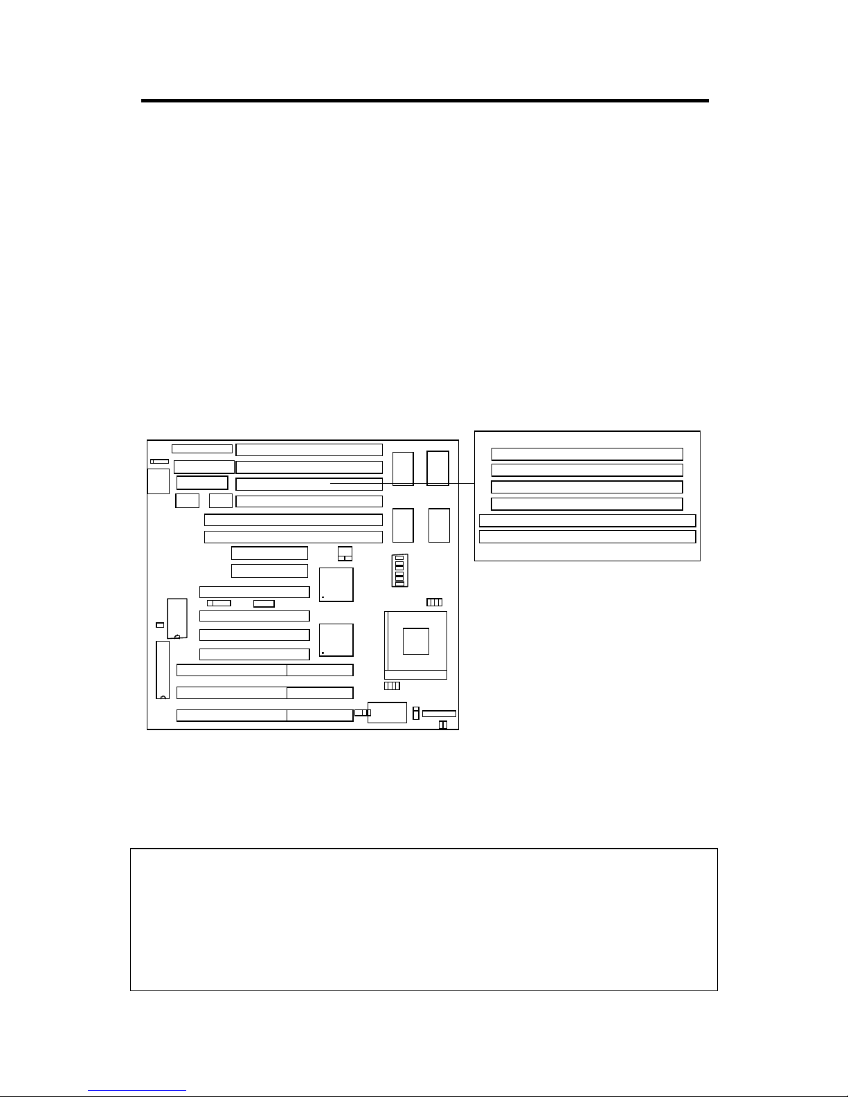
CHAPTER 1 INTRODUCTION
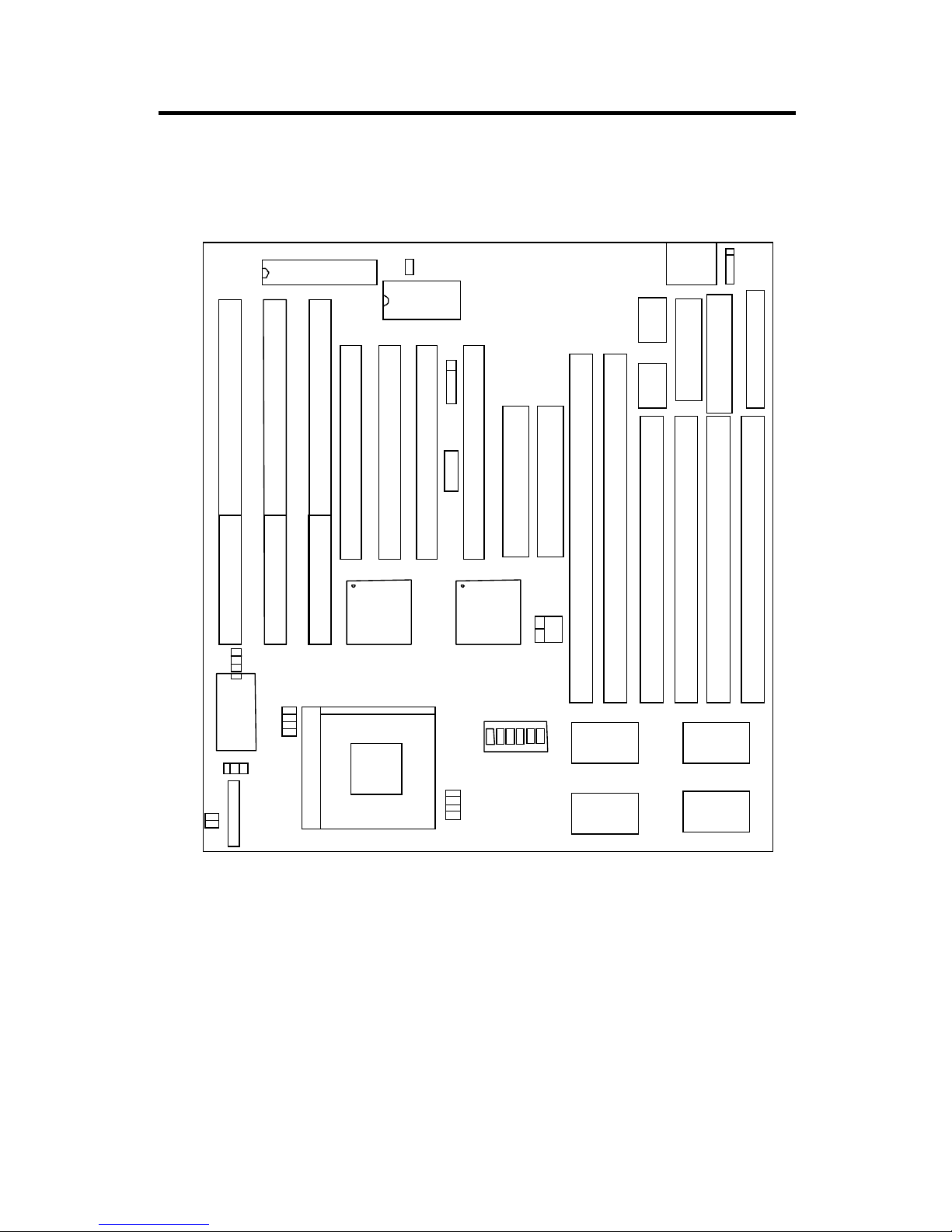
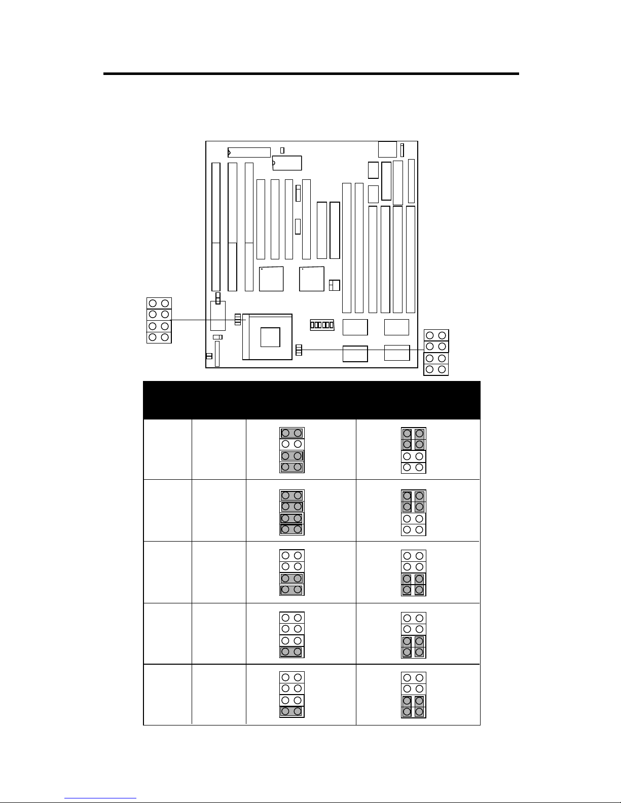
1.3 System Board Layout
1-3
SIMM1
FDD
PRN
COM1
DIMM2
DIMM1
HDD1
HDD2
437VX
JFAN
371SB
+ -
438VX
SRAM
438VX
SRAM
KBC
RTC
ATKBD
ISA 3
USB1
IR
JRTC1
+5V +3V
J2
JGL 1
JGS1
JFM1
JM1
SOCKET 7
ON
DIP
121
3
415
6
1
BIOS
SIMM2
SIMM3
SIMM4
COM2
Power Connector
JP1
JV1
JV2
JV3
JV4
1
SW1
ISA 2
ISA 1
PCI 3
PCI 4
PCI 2
PCI 1
JV5
MS-5149
CHAPTER 2 HARDWARE INSTALLATION
Chapter 2
Hardware Installation
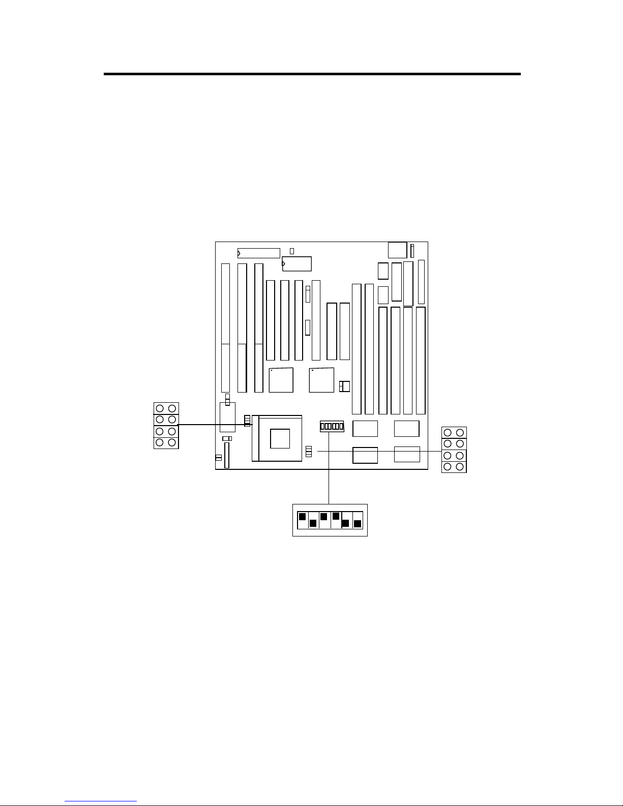
2.1 Central Processing Unit: CPU
The MS-5149 motherboard operates with Intel® Pentium® processors/
Pentium® processor with MMX technology, Cyrix® 6x86/6x86L/6x86MX,
and AMD® 5K86/K6 processors. It could operate with 2.8V to 3.52V
processors. The motherboard provides a 321-pin ZIF Socket 7 for easy CPU
installation, a DIP switch (SW1) to set the proper speed for the CPU and a
Jumper block (JV1 - JV4, JV5) for setting the CPU voltage. The CPU should
always have a cooling fan attached to prevent overheating.
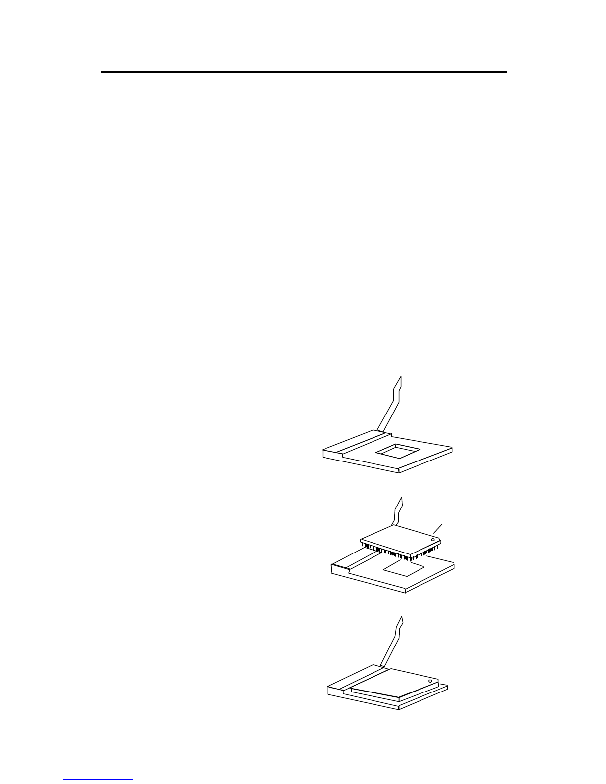
2.1-1 CPU Installation Procedure
1 . Pull the lever sideways away
from the socket. Then raise
the lever up to a 90-degree
angle.
3. Press the lever down to
complete the installation.
2 . Locate Pin 1 in the socket
and look for the white dot or
cut edge in the CPU. Match
Pin 1 with the white dot/cut
edge. Then insert the CPU.
It should insert easily.
CPU
CPU
Open Lever
Pin 1
Sliding
Plate
White dot/
Cut edge
Close
Lever
2-1
CHAPTER 2 HARDWARE INSTALLATION
1. The 4 CPU clock frequencies that the system supports are 50 MHz,
55MHz, 60MHz and 66.6MHz (To adjust SW1 pin 1, 2 , and 3). See the
following chart to set the different Host Clock Frequencies.
1 2 3 CLOCK
ON ON OFF 50MHz
OFF O N OFF 55MHz
ON OFF OFF 60MHz
OFF OFF OFF 66.6MHz
SW1 CPU
2 . The DIP Switch SW1 (4, 5 and 6) is used to set the Core/Bus (Fraction)
ratio of the CPU. The actual core speed of the CPU is the Host Clock
Frequency multiplied by the Core/Bus ratio. For example:
If CPU Clock = 66.6MHz
Core/Bus ratio = 3/ 2
then CPU core speed = Host Clock x Core/Bus ratio
= 66.6MHz x 3/2
= 100MHz
3. The PCI Bus Clock is the CPU Clock Frequency divided by 2.
2.1-2 CPU Core Speed Derivation Procedure
2-2
4 5 6 Core/Bus Ratio
OFF OFF OFF 1.5
ON OFF OFF 2
ON ON OFF 2.5
OFF ON OFF 3
OFF ON OFF 3
OFF OFF OFF 3.5
SW1
CPU
Shaded Part are used by Intel® Pentium® processor
with MMXTM technology and AMD® K6
Note:
CHAPTER 2 HARDWARE INSTALLATION
2.1-3 CPU Voltage Setting: JV1 - JV4, JV5
JV1~JV4VcoreV I/O
3.3 3.3
3.5
3.5
3.3
3.2
SIMM1
FDD
PRN
COM1
DIMM2
DIMM1
HDD1
HDD2
437VX
JFAN
371SB
+ -
438VX
SRAM
438VX
SRAM
KBC
RTC
ATKBD
ISA 3
USB1
IR
JRTC1
+5V +3V
J2
JGL 1
JGS1
JFM1
JM1
SOCKET 7
ON
DIP
121
3
4
1
5
6
1
BIOS
SIMM2
SIMM3
SIMM4
COM2
Power Connector
JP1
JV1
JV2
JV3
JV4
JV5
SW1
ISA 2
ISA 1
PCI 3
PCI 4
PCI 2
PCI 1
JV1
JV2
JV3
JV4
JV5
JV5
3.3
2.8
3.3 2.9
JV1
JV2
JV3
JV4
JV1
JV2
JV3
JV4
JV1
JV2
JV3
JV4
JV1
JV2
JV3
JV4
2-3
12
7
8
1
2
78
12
7
8
1
2
7
8
1
2
7
8
JV1
JV2
JV3
JV4
CHAPTER 2 HARDWARE INSTALLATION
2.1-3 CPU Speed and Voltage Setting: SW1 & JV1-JV4, JV5
To adjust the speed and voltage of the CPU, you must know the specification of your CPU (always ask the vendor for CPU specificaton). Then refer
to Table 2.1 (Intel® processors), T able 2.2 (Cyrix® processors) and T able
2.3 (AMD® processors) for proper setting.
SW1
1 2 3 4 5 6
ON
ON
OFF
Speed Setting
SIMM1
FDD
PRN
COM1
DIMM2
DIMM1
HDD1
HDD2
437VX
JFAN
371SB
+ -
438VX
SRAM
438VX
SRAM
KBC
RTC
ATKBD
ISA 3
USB1
IR
JRTC1
+5V +3V
J2
JGL 1
JGS1
JFM1
JM1
SOCKET 7
ON
DIP
121
3
4
1
5
6
1
BIOS
SIMM2
SIMM3
SIMM4
COM2
Power Connector
JP1
JV1
JV2
JV3
JV4
JV5
SW1
ISA 2
ISA 1
PCI 3
PCI 4
PCI 2
PCI 1
JV1
JV2
JV3
JV4
JV5
2-4
CHAPTER 2 HARDWARE INSTALLATION
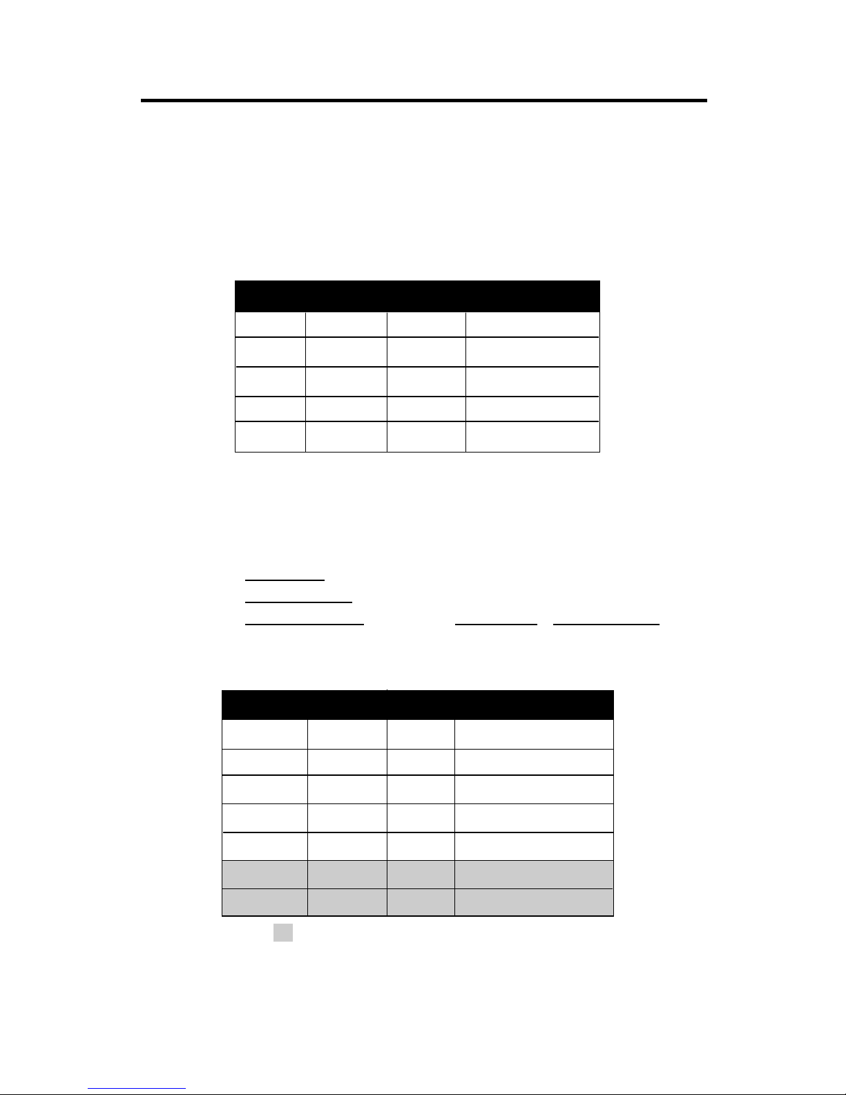
Table 2.1 Intel® Pentium® processors
ON DIP
123 456
ON
OFF
90MHz
100MHz
120MHz
133MHz
150MHz
166MHz
200MHz
3.3
3.5
3.5
3.3
3.3
3.5
3.5
ON DIP
123 456
ON
OFF
ON DIP
123 456
ON
OFF
ON DIP
123 456
ON
OFF
ON DIP
123 456
ON
OFF
ON DIP
123 456
ON
OFF
75MHz
3.3
CPU Type
CPU SpeedCPU Voltage
SW1
JV1~JV4
VI/O Vcore
JV5
2-5
12
7
8
12
78
12
78
12
78
JV1
JV2
JV3
JV4
JV1
JV2
JV3
JV4
JV1
JV2
JV3
JV4
JV1
JV2
JV3
JV4
ON DIP
123 456
ON
OFF
166MHz
200MHz
233MHz
3.5
ON DIP
123 456
ON
OFF
3.3
2.8
12
78
ON DIP
123 456
ON
OFF
ON DIP
123 456
ON
OFF
JV1
JV2
JV3
JV4
ON DIP
123 456
ON
OFF
a. Intel® Pentium
®
processors
b. Intel® Pentium
®
processors with MMXTM technology

CHAPTER 2 HARDWARE INSTALLATION
Table 2.2 Cyrix® 6x86 processor
Cyrix® processor uses PR to rate the speed of their processors based on
Intel® processor core speed. For example P120+ (100MHz) has 120MHz core
speed of an Intel® processor but has 100MHz core speed in Cyrix® processor .
Cyrix® processor should always uses a more powerful fan (ask vendor for
proper cooling fan).
ON DIP
123 456
ON
OFF
3.5
ON DIP
123 456
ON
OFF
ON DIP
123 456
ON
OFF
P120+
(100MHz)
CPU Type
CPU SpeedCPU Voltage
SW1
JV1~JV4
VI/O Vcore
P133+
(110MHz)
P150+
(120MHz)
P166+
(133MHz)
ON DIP
123 456
ON
OFF
JV5
Cyrix® 6x86L processor
3.3
PR166
(166MHz)
ON DIP
123 456
ON
OFF
2.8
2-6
12
78
12
78
JV1
JV2
JV3
JV4
JV1
JV2
JV3
JV4
Cyrix® 6x86MX processor
3.3
PR166
2.9
12
78
JV1
JV2
JV3
JV4
*PR200
*PR233
ON DIP
123 456
ON
OFF
ON DIP
123 456
ON
OFF
ON DIP
123 456
ON
OFF
Note: * This CPU type is reserved for future support.
CHAPTER 2 HARDWARE INSTALLATION
Table 2.3 AMD® K5 processor
AMD® K5 processor uses PR to rate the speed of their processors based on
Intel® processor core speed. For example: P133+ (100MHz) has 133MHz core
speed of Intel® processor but has 100MHz core speed in AMD® processor.
AMD® processor should always uses a more powerful fan (ask vendor for
proper cooling fan).
ON DIP
123 456
ON
OFF
3.5
ON DIP
123 456
ON
OFF
ON DIP
123 456
ON
OFF
CPU Type
CPU SpeedCPU Voltage
SW1JV1~JV4VI/O Vcore
PR90
(90MHz)
PR100
(100MHz)
PR133
(133MHz)
ON DIP
123 456
ON
OFF
PR166
(166MHz)
JV5
AMD® K6 processor
3.3
PR166
(166MHz)
ON DIP
123 456
ON
OFF
PR200
(200MHz)
2.9
2-7
ON DIP
123 456
ON
OFF
12
78
12
78
JV1
JV2
JV3
JV4
JV1
JV2
JV3
JV4

CHAPTER 2 HARDWARE INSTALLATION
2.1-4 CPU Fan Power Connector: JFAN
This connector supports CPU cooling fan with +12V. It supports both two
and three pin head connector. When connecting the wire to the connector,
always take note that the red wire is the positive and should be connected to
the +12V .
JFAN
Connector
+12V
GND
GND
Recommended CPU cooling fan specification:
- Metallic Clip
- RPM 5000
- CFM 10
- +12V
- 52x52x10mm
- Ball Bearing
Note: Always consult vendor for
proper CPU cooling fan.
2-8
SIMM1
FDD
PRN
COM1
DIMM2
DIMM1
HDD1
HDD2
437VX
JFAN
371SB
+ -
438VX
SRAM
438VX
SRAM
KBC
RTC
ATKBD
ISA 3
USB1
IR
JRTC1
+5V +3V
J2
JGL 1
JGS1
JFM1
JM1
SOCKET 7
ON
DIP
121
3
4
1
5
6
1
BIOS
SIMM2
SIMM3
SIMM4
COM2
Power Connector
JP1
JV1
JV2
JV3
JV4
1
SW1
ISA 2
ISA 1
PCI 3
PCI 4
PCI 2
PCI 1
JV5
CHAPTER 2 HARDWARE INSTALLATION
2.1-5 CMOS RAM Clear: JRTC
This jumper is for clearing the R TC data.
JRTC
keep Data
(default)
clear
SIMM1
FDD
PRN
COM1
DIMM2
DIMM1
HDD1
HDD2
437VX
JFAN
371SB
+ -
438VX
SRAM
438VX
SRAM
KBC
RTC
ATKBD
ISA 3
USB1
IR
JRTC1
+5V +3V
J2
JGL 1
JGS1
JFM1
JM1
SOCKET 7
ON
DIP
121
3
4
1
5
6
1
BIOS
SIMM2
SIMM3
SIMM4
COM2
Power Connector
JP1
JV1
JV2
JV3
JV4
JV5
SW1
ISA 2
ISA 1
PCI 3
PCI 4
PCI 2
PCI 1
2-9
CHAPTER 2 HARDWARE INSTALLATION
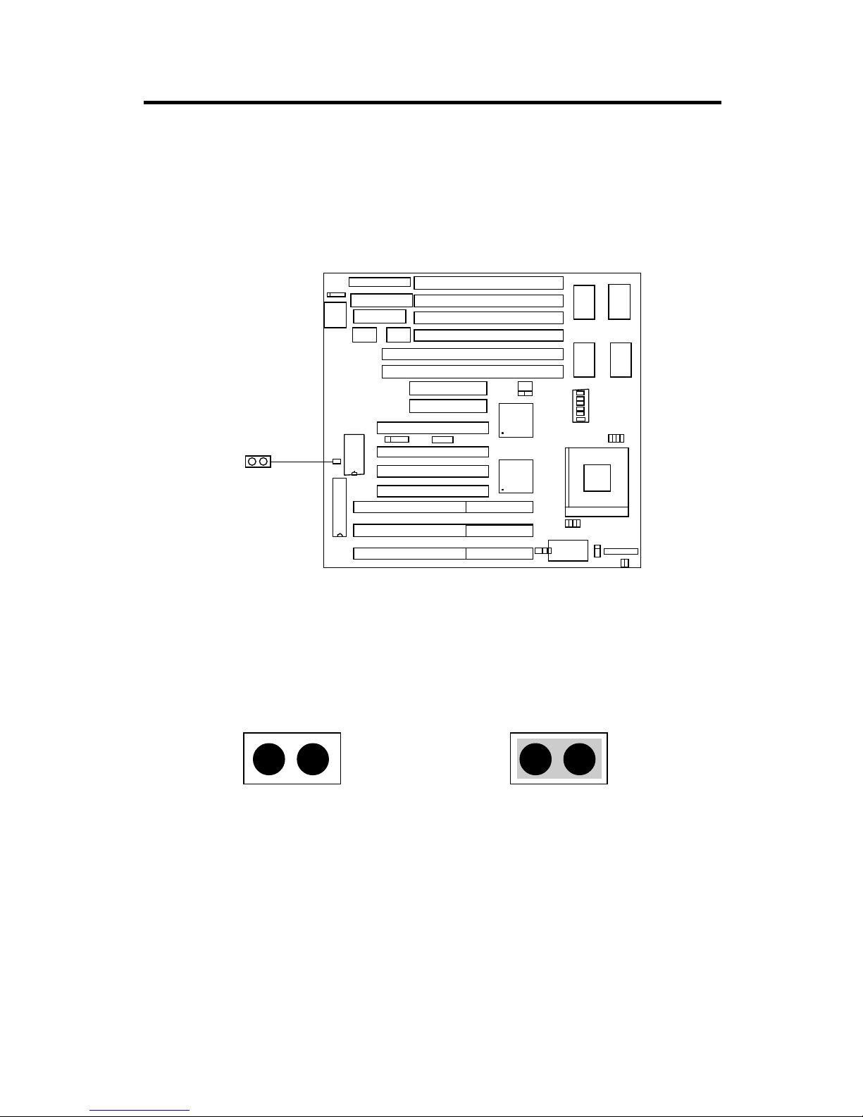
2.2 Memory Installation
2.2-1 Memory Bank Configuration
The system board supports a maximum of 128M of memory . It provides four
72-pin SIMMs (Single In-Line Memory Module) and two 168-pin DIMM
sockets. This board supports 4 banks wherein each bank supports memory
ranging from 4MB to 32MB. A Bank always has a pair of SIMM or a single
DIMM. Each bank supports 4M, 8M, 16M and 32M. The 2MB is the
minimum and the 16MB is the maximum for one 72-pin single sided memory
module.
W arning! SIMM Socket 1-4 power level is 5 volts. DIMM Socket 1 & 2
power level is 3.3 V/5V. W e suggest not to install both the SIMM
& DIMM at the same time. But if you want to install both SIMM
& DIMM slot, you must use a 3.3 volt DIMM with 5 volt I/O
signal tolerance or use a full 5 volt DIMM module. Otherwise it
may cause damage to the DIMM.
SIMM4(Bank 2/3) RAS2+ RAS3
SIMM3(Bank 2/3) RAS2+ RAS3
SIMM2(Bank 0/1) RAS0+ RAS1
SIMM1(Bank 0/1) RAS0+ RAS1
DIMM2(Bank 0/1) RAS1+ RAS0
DIMM1(Bank 2/3) RAS3+ RAS2
SIMM1
FDD
PRN
COM1
DIMM2
DIMM1
HDD1
HDD2
437VX
JFAN
371SB
+ -
438VX
SRAM
438VX
SRAM
KBC
RTC
ATKBD
ISA 3
USB1
IR
JRTC1
+5V +3V
J2
JGL 1
JGS1
JFM1
JM1
SOCKET 7
ON
DIP
121
3
4
1
5
6
1
BIOS
SIMM2
SIMM3
SIMM4
COM2
Power Connector
JP1
JV1
JV2
JV3
JV4
JV5
SW1
ISA 2
ISA 1
PCI 3
PCI 4
PCI 2
PCI 1
2-10
CHAPTER 2 HARDWARE INSTALLATION
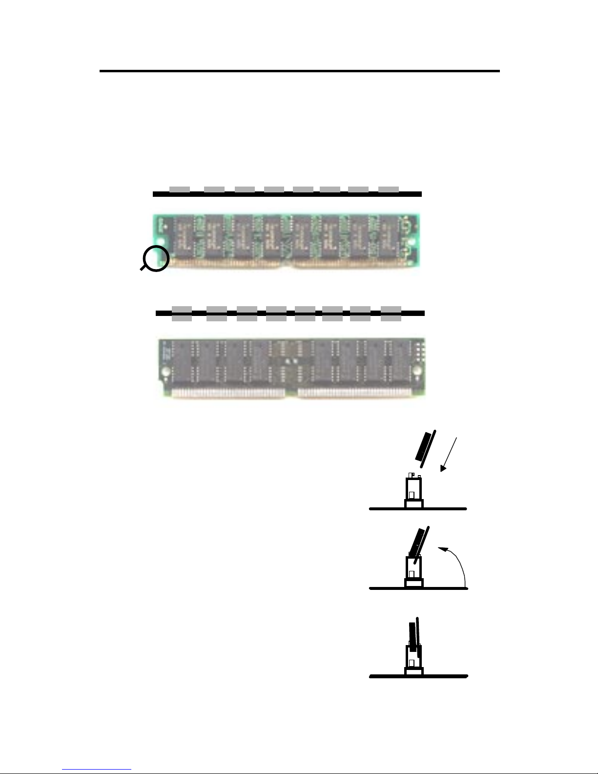
2.2-2 Memory Installation Procedures:
1. The SIMM slot has a “Plastic Safety
Tab” and the SIMM memory module
has a “Notched End”, so the SIMM
memory module can only fit in one
direction.
2. Insert the SIMM memory modules into
the socket at 45-degree angle. Then
push into a vertical position so that it
will snap into place.
3. The Mounting Holes and Metal Clips
should fit over the edge and hold the
SIMM memory modules in place.
A. How to install a SIMM Module
Single Sided SIMM
Double Sided SIMM
Note: Always use a 5 volts SIMM with 70 ns
or above(Fast Page or EDO)
Notched
End
2-11
CHAPTER 2 HARDWARE INSTALLATION
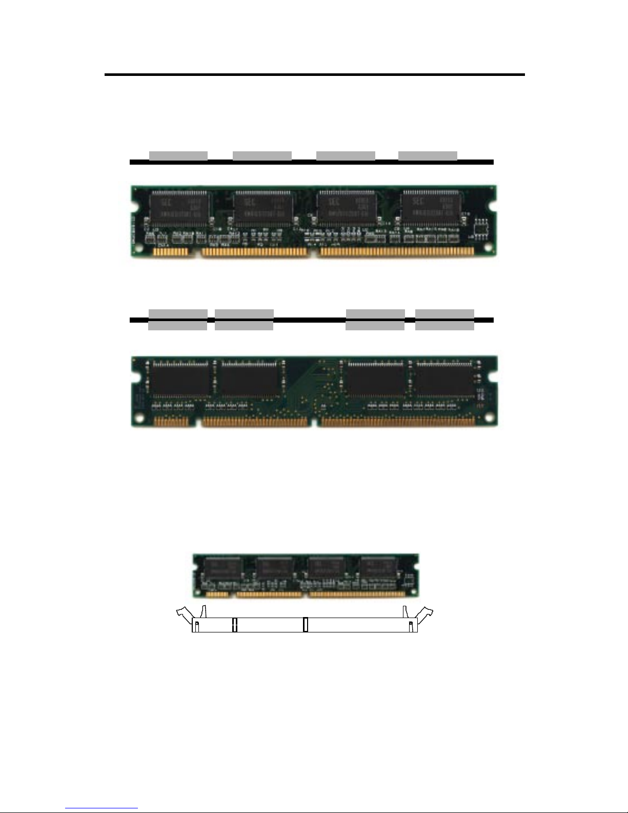
B. How to install a DIMM Module
1. The DIMM slot has a two key mark “VOLT and DRAM” , so the
DIMM memory module can only fit in one direction.
2. Insert the DIMM memory module vertically into the DIMM slot.
Then, push it in.
3. Close the plastic clip at the side of the DIMM slot.
Single Sided DIMM
Double Sided DIMM
2-12
Note: If you have installed SIMM and DIMM at the same time, you must
use a 3.3 volt DIMM with 5 volt I/O signal tolerance or a full 5 volt
DIMM module (EDO, FP or SDRAM). Look for J2 to select the
DIMM voltage.
 Loading...