

Page 1
Edit
martinhuang
Data
November. 16, 2007
Ver
0A
0
GGXX77220
Trouble Shooting Guide
PPrroojjeecctt NNaammee:: MMSS--11772222
MMaarrkkeettiinngg NNaammee:: GGXX772200
Page 2

1
Contents
1. Introduction………………………………………………………………………………………………2
1.1 Overview
1.2 MS-1722 Product Specification (Intel Penryn / Quad core processor
(45 nm; dual core)+Cantiga + ICH9M MXM)
2. System Architecture……………………………………………………………………………………6
2.1 Block Diagram
2.2 PCB Assembly Description
3. Power Map & Repair Flow Chart………………………………………………………………………8
3.1 Power Map
3.2 Repair Flow Chart
4. Clock Map & Repair Flow Chart………………………………………………………………………18
4.1 Clock Map
4.2 Repair Flow Chart
5. System Reset Map & Repair Flow Chart……………………………………………………………25
6. Power On Sequence……………………………………………………………………………………27
7. AMI BIOS Check Point List ……………………………………………………………………………29
Page 3
2
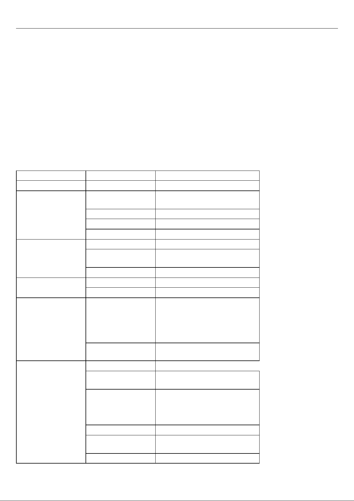
Item
H/W Spec
Model
Spindle
2
Support Processor @
Launch
Intel Penryn / Quad core
processor (45 nm; dual core)
L2 Cache
3MB/ 6MB,
FSB Speed
support 667/800/1066 MHz
Socket
478 pins
Memory
Technology
DDRII 667 / 800
Memory
DDRII SO-DIMM X 2 slot
512/1024/2048 MB
(Max.)
4GB (2GB DDRII SO-DIMM x 2)
CoreChip
North Bridge
Cantiga
South Bridge
ICH9M
Display
LCD Type
17” 1. WUXGA (1920x1200)-non
glare 2. WSXGA
(1680x1050)-glare 3. WXGA+
(1440 x 900) TFT LCD
display-Glare.
Brightness
Brightness controlled by K/B
hot-keys
Video (MXM spec)
Controller
NB-9E GS
VRAM
16Mx32 -1.4ns by 8 pcs = 512M
GDDR3
LCD
1. WSXGA (1680x1050) 2.
WXGA+ (1440 x 900) 3. WUXGA
(1920x1200) waiting for
spec ,9/E
HDMI
HDMI 1.3 support
DVI-D
DVI can use HDMI adapter to
transfer
CRT
waiting for spec ,9/E
1、Introduction
1.1 Overview
MS-1722 notebook computer provide Intel® Montevina platform design contains: Celeron processor
on 45 nanometer process and Crestline chipset Cantiga + ICH9M MXM.
Intel® processor , 17" TFT ,removable HDD , build in Combo /DVDRW ,USB2.0,on board Giga LAN,
MDC , Bluetooth, Mini card for Intel 802.11b/g/n wireless LAN,IEEE1394 , 6 in 1 Card reader, Audio….
1.2 MS-1722 Product Specification (Cantiga + ICH9M MXM)
Page 4
3
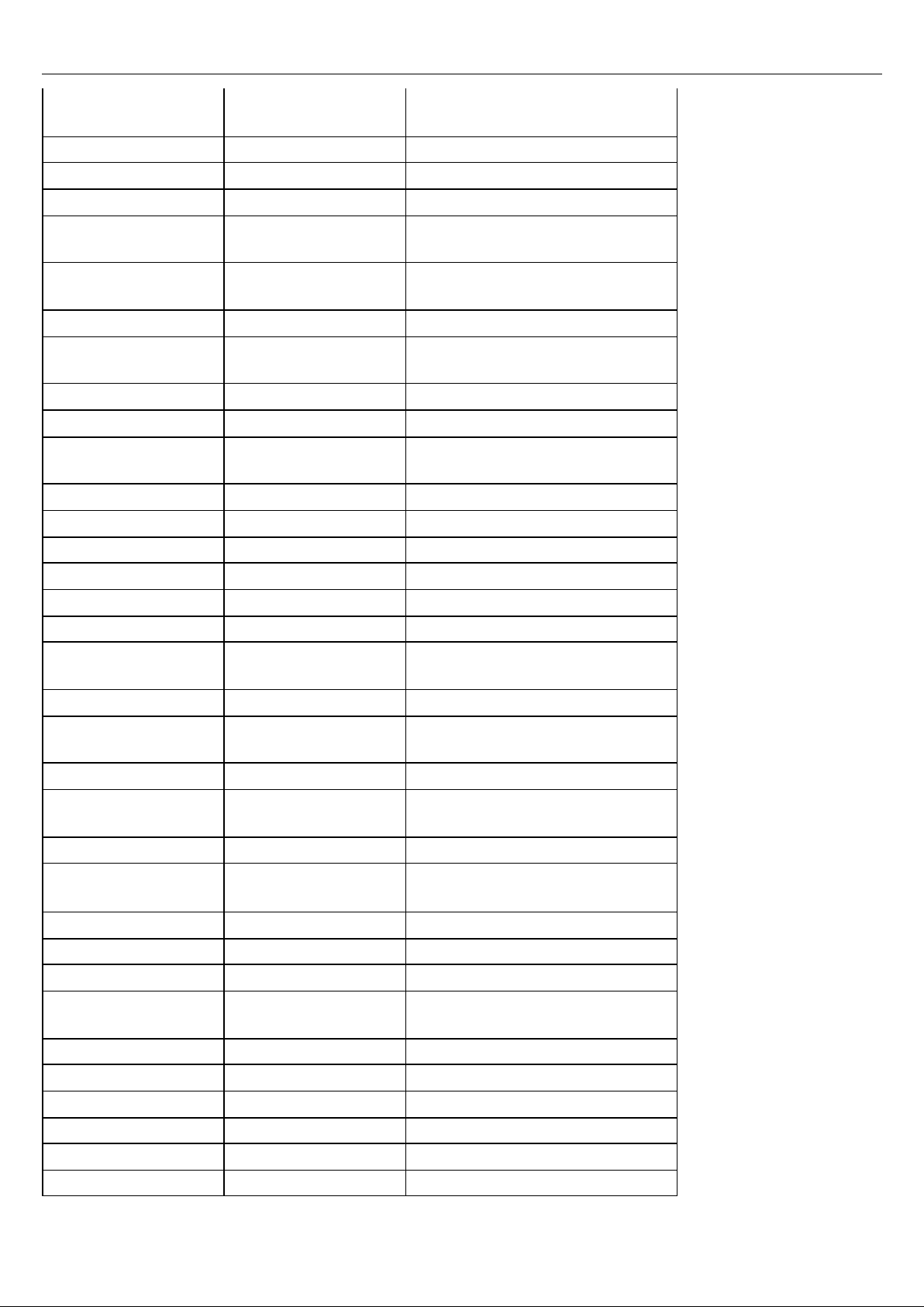
Dual-View functions
CRT + DVI/HDMI, LCD+CRT,
LCD+HDMI
Audio
Sound Codec chip
Azalia interface,ALC 888
Internal Speaker
4 Speakers 2Wx4 + subwoofer
HW Wave Table MIDI
S/W wave table
4 connectors,
definition ->
Analog 7.1 channel
output
Support
Digit 7.1
SPDIF by Headphone out
Sound Volume
Adjust by volume button, K/B
function-key & SW
Line-In
x 1
Mic-in
x 1
Headphone out
/SPDIF out
x 1
Side out
x 1
Internal macrophone
x 1 ("Analog" Mic)
MDC
56K Fax/MODEM
MDC ML3054
I/F
Azalia Modem
Controller
Azalia Embedded
Wake on Ring
Support on S3/S4/S5 state, AC
Module only
PTT Approval
Yes (FCC/CTR21/JATE)
Wake on LAN
Support on S3/S4/S5 state , AC
module only
WfM
Wfm 2.0 support
LAN
10/100/1000 Base on board
LAN
Communication Port
optional
Wireless Lan
TWINHAN AW-GE780 /Intel
solutions(WIFI)
optional
Bluetooth
EDR 2.0
RJ45
x 1
RJ11
x 1
Card Reader
4 in 1 Card Reader SD MMC MS
XD
IEEE1394
x 1
Express Card
x 1
USB
x 4 (Ver. 2.0)
Camera 2.0M pixel
x 1
E-SATA
x 1
Mini PCI-E Card
x 3
Page 5
4
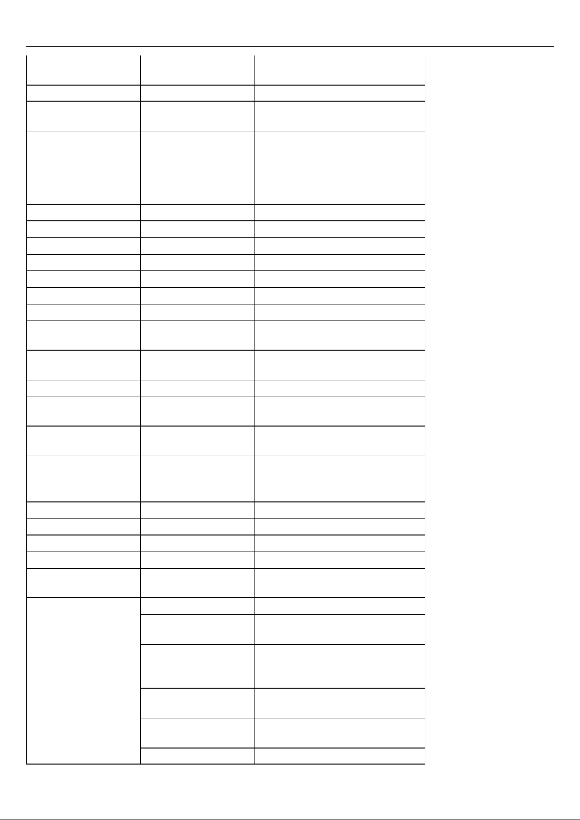
optional
TV-tuner
x 1 (PCI-Express I/F) , support
Analog/Digit/Hybrid TV-tuner
Storage
HDD form factor
2.5" 9.5mm height, SATA
interface 5400/7200RPM
Optical drive
5.25" 12.7 mm height DVD
Super Multi , Blu-Ray, HD-DVD
(SATA)
(need to confirm cost difference)
Remote Controll
IR Receive
Infrared Frequency 38Khz
optional
IR Decode
yes (supported by ENE 3925)
Remote Controller
Vista Slim Express Card Type
Keyboard
Controller (KBC)
ENE (3925)
KeyPitch/Stroke
19mm Pitch / 2.5mm stroke
MS Standard key
code
Support
Number of Keys
Gaming k/b 103 (same as 163A)
Dual Display
Fn + F2
Touch Pad enable /
disable
Fn + F3
LCD brightness Down
Fn + F4
LCD brightness UP
Fn + F5
Speaker Volume
Down
Fn + F7
Speaker Volume UP
Fn + F8
Speaker ON/OFF
Fn + F9
Sleep Button(S3)
Fn + F12
Short-cut Keys
Hot key
PWR, WLAN/BT, Turbo ,
Webcam, P1
Power
AC Adapter
19V 120w
1st Battery
9 cell, 7200 mAh
6 cell, 4800 mAh
1st Battery Life
(battery life based on
Anne's definition)
6 Cell / 9 cell TBD
Battery Life in stand
by mode
72 hr (S3, battery, by 9 cell)
S4/S5: 1 month, Hibernation
mode
RTC Battery
Yes , 3 yrs
Page 6
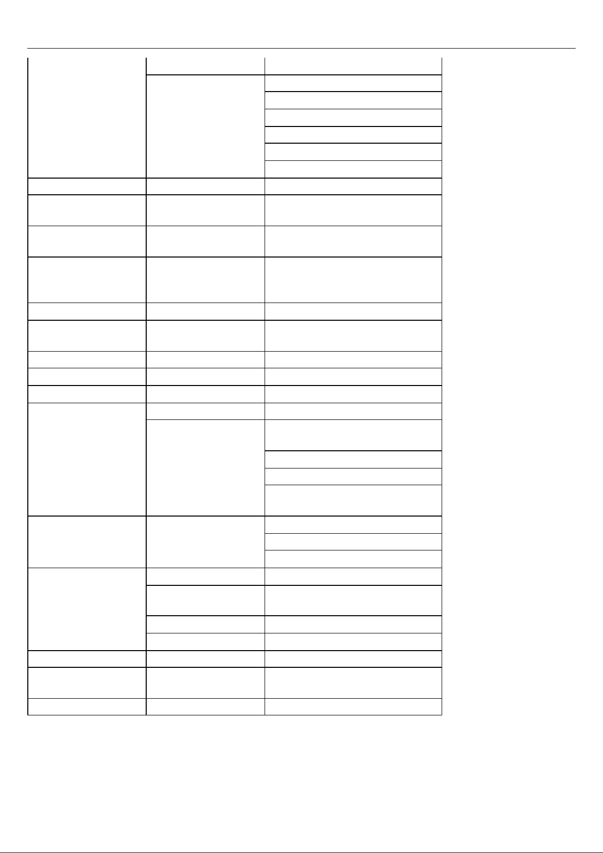
5
Status Indicator
Indicator
Power
ask EC to define
indicator
HDD
Battery
Number Lock
Caps Lock
Scroll Lock
WI-FI/BT
Other
USB connecters
Supply Power (S0 ~S1)
Physical
Characteristics
Dimension
395.0(W) x 278.0(D) x
33.5(H)mm/39.5 mm
Weight
Target under 3.6Kg with 6 cell
Battery
Compliance
WHQL
Windows Vista Home
Basic/Home Peruim/Business
Software
Support OS
Vista , 32-bit & 64-bit OS
USB Flash boot
Yes, USB floppy boot up DOS
only (MSI USB dongle/ MP3)
BIOS
Fast Boot Support
Yes (Win Vista)
Power Management
ACPI 1.0b & 2.0
Yes
SMBIOS
2.3X
EMC
EMS
CE Mark (Europe)
EMI (ask Sale to
commit a q'ty)
FCC Class B Certified (USA &
Canada)
BSMI (Taiwan)
CE Mark / C-tick/ A-tick
CCC (PRC), MIC (Korea), Gost
(Russia), VCCI (Japan)
Safety
Safety (ask Sale to
commit a q'ty)
UL, (CUL) (USA & Canada)
TUV(Germany)
TUV-CB Report (Europe)
RF
USA, Canada, Taiwan, China,
Europe (Germany, France, Italy,
Spain, UK)
Telecomm.
FCC Part 68 (USA & Canada)
CTR 21 (Europe), JATE (Japan)
1st priority
US, Canada
2nd priority
UK, GR, FR, Italy, Spain, China,
Korea, JP
Energy Star
Supported
Page 7
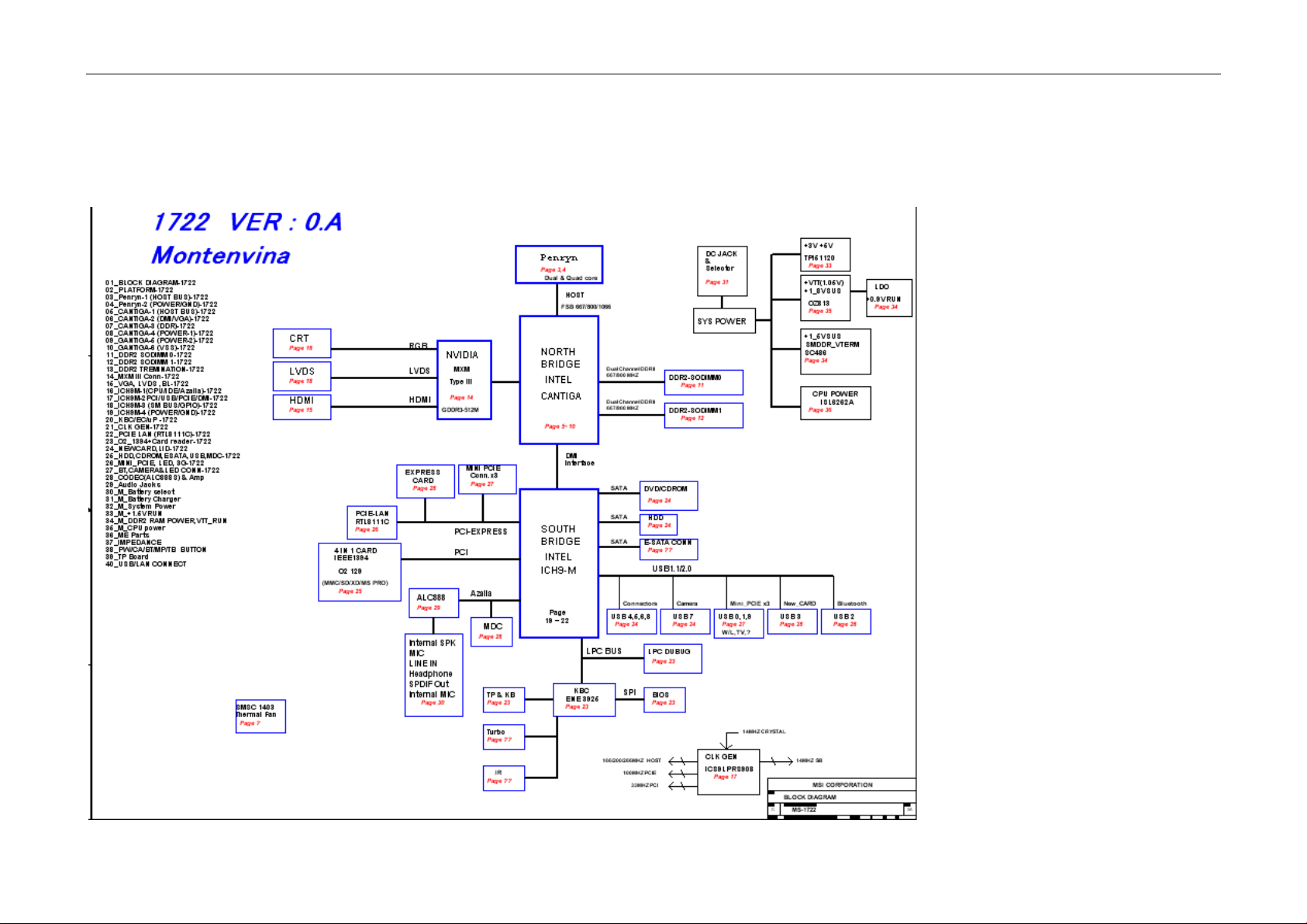
6
2、System Architecture
2.1 Block Diagram
Page 8
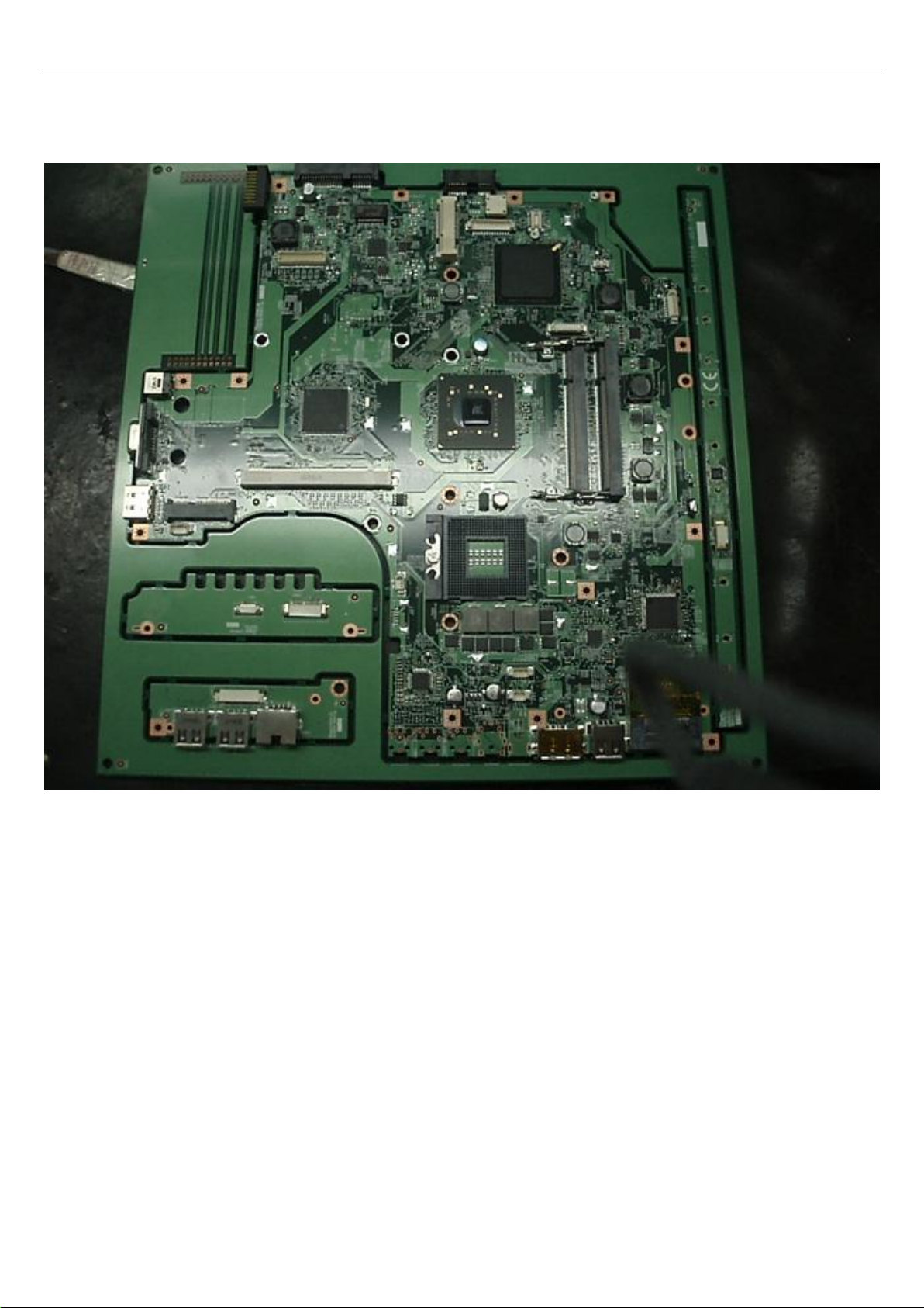
7
2.2 PCB Assembly Description
Top View
Page 9
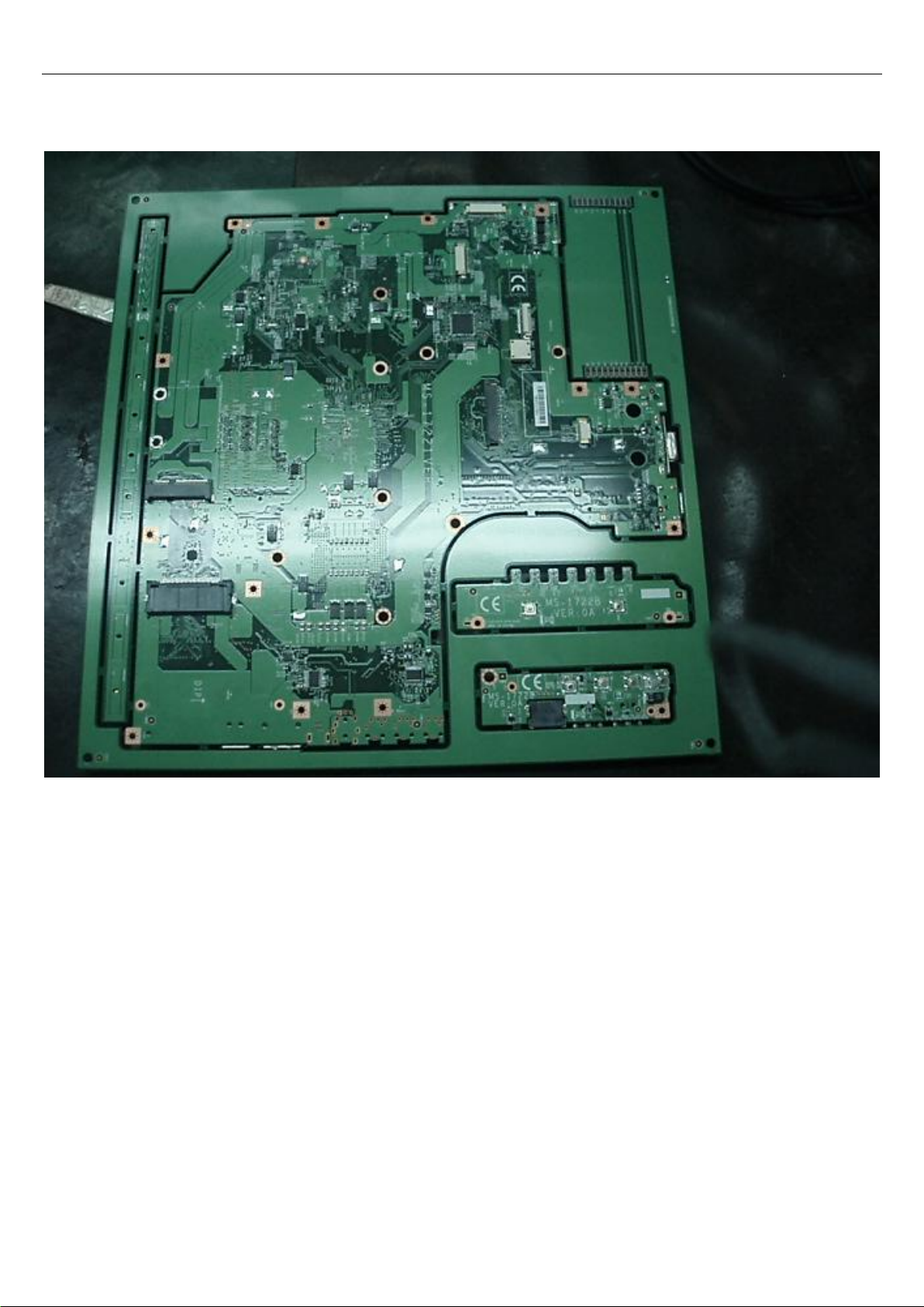
8
Bottom View
Page 10
9
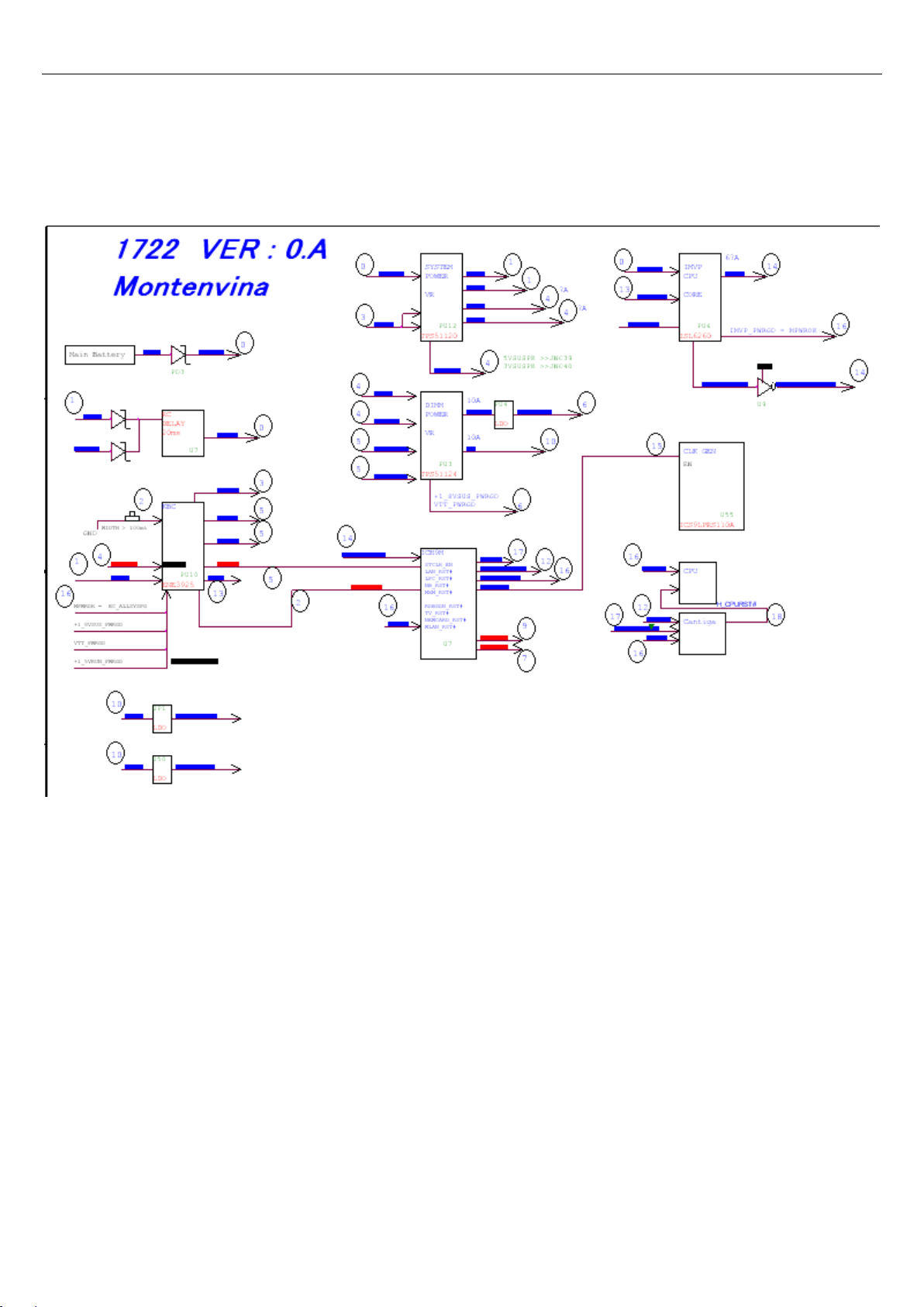
3、Power Map & Repair Flow Chart
3.1、POWER MAP
Page 11
10
Item
Name
Description
Check Component
(related signal)
Note
1-1
ADAPTER_IN
DC19V
PJ1 : PIN1
1-2
DACKING_IN
DC9.5V
PQ24 : PIN 5
1-3
DC_IN+
DC19V
PQ1 : PIN 5
1-4
SDC_IN+
DC19V
PQ7 : PIN 5
1-5
V_CHG
DC0V
PQ4B : PIN 5
When battery charge, the voltage value is
DC12.6V
1-6
PWR_SRC
DC19V
PQ24 : PIN 1
Item
Name
Description
Check Component
(related signal)
Note
2-1
+5VALW
DC5V
PD6 : PIN3
2-2
+3VALW
DC3.3V
PU2 : PIN19
2-3
RTCVCC
DC3.3V
D3 : PIN3
2-4
RTCRST
L>H(DC3.3V)
U7: PIN25
2-6
Y1
32.768KHZ
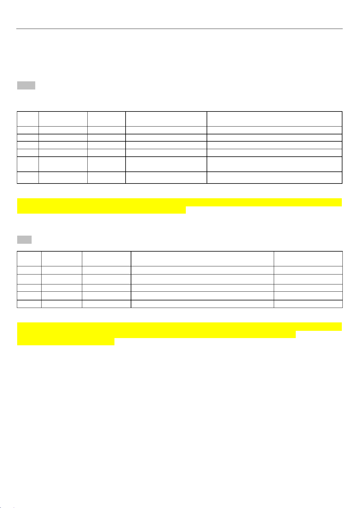
3.2 Repair Flow Chart
Debug by power sequence(Only insert adapter):
Please follow below step to check power source
Step 1、MAIN Power(PWR_SRC)
Note 1:It is recommendation to check the PWR_SRC (Power) first. If the power is right, you can check the next step
directly. If the power is fault, please check the related signal.
Step 2、3VALW & 5VALW & RTCVCC
Note 1:It is recommendation to check the +5VALW、+3VALW、RTCVCC(Power) & Y2 (clock) first. If these power are
right, you can check the next step directly. If these signals are fault, please check the related signal.
Note 2: The L > H signal is H level.
Page 12
11
Item
Name
Description
Check Component
(related signal)
Note
3-1
PWR_SW-
Push bottom at least 50ms
H > L( DC0V)
U10: PIN43
3-3
SUS_ON
L > H(DC3.3V)
U10: PIN108
3-4
+5VSUS
DC5V
PQ14 : PIN 5
3-5
+3VSUS
DC3.3V
PQ15 : PIN 5
3-6
SUSPWROK
SUS Power OK
L > H(DC3.3V)
R283
Item
Name
Description
Check Component
(related signal)
Note
4-1
RSMRST#
L > H(DC3.3V)
R159
4-2
PM_SLP_S5#
L > H(DC3.3V)
U7(TP53)
Have not used
4-3
PM_SLP_S4#
L > H(DC3.3V)
Jnc18
4-4
+1_8VDIMM
DC1.8V
PQ19 : PIN 5
4-6
SMDDR_VTERM
DC0.9V
Pc83
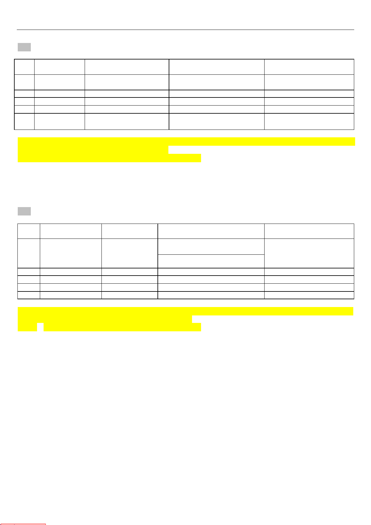
Step3、SUS Power
Note 1:It is recommendation to check the SUSPWROK first. If this signal is right, you can check the next step directly.
If this signal is fault, please check the related signal.
Note 2:The L > H signal is H level;The H > L signal is L level
Step4、DDR2 Power
Note 1:It is recommendation to check the SMDDR_VTERM first. If this signal is right, you can check the next step
directly. If this signal is fault, please check the related signal.
Note 2:The L > H signal is H level;The H > L signal is L level
Page 13
12
Item
Name
Description
Check Component
(related signal)
Note
5-1
PM_SLP_S3#
L > H(DC3.3V)
JNC17
5-2
CLK_PWRGD
DC
U7 : PIN R5
5-3
RUND
DC 17.75V
PR50
5-4
+1_2VSUS
DC1.20V
U50 : PIN 4
5-5
VTT
DC1.05V
PC210
5-6
VTT_PWRGD &
+1_8VSUS_PW
RGD
Power Good
L > H(DC3.3V)
PR91/PR86
5-7
MPWROK
Power OK
L > H(DC3.3V)
R654
5-8
ALLSYSPG
ALL Power Good
L > H(DC3.3V)
R170
5-9
+1_5VRUN
DC1.5V
PC206
5-10
+3VCLKGEN
DC3.3V
R722
5-11
ADD5V
DC5V
L94(Codec Power)
5-12
+1.2VRUN
DC1.2V
PR141
5-13
+3VRUN
DC3.3V
PQ15,PIN 1
5-14
+5VRUN
DC5V
PQ14,PIN 1
5-15
+1_5VRUN_PW
RGD
Power Good
L > H(DC3.3V)
PR76
At the same time change the
status
Item
Name
Description
Check Component
(related signal)
Note
6-1
VR_ON
L > H(DC3.3V)
JNC52
6-2
V_CORE
Control by VID[6:0]
PC148(CPU Power)
6-3
VR_PWRGD_CLKEN#
H > L(DC0V)
U9,PIN 2
6-4
IMVP_PWRGD
PWROK
L > H(DC3.3V)
PR80
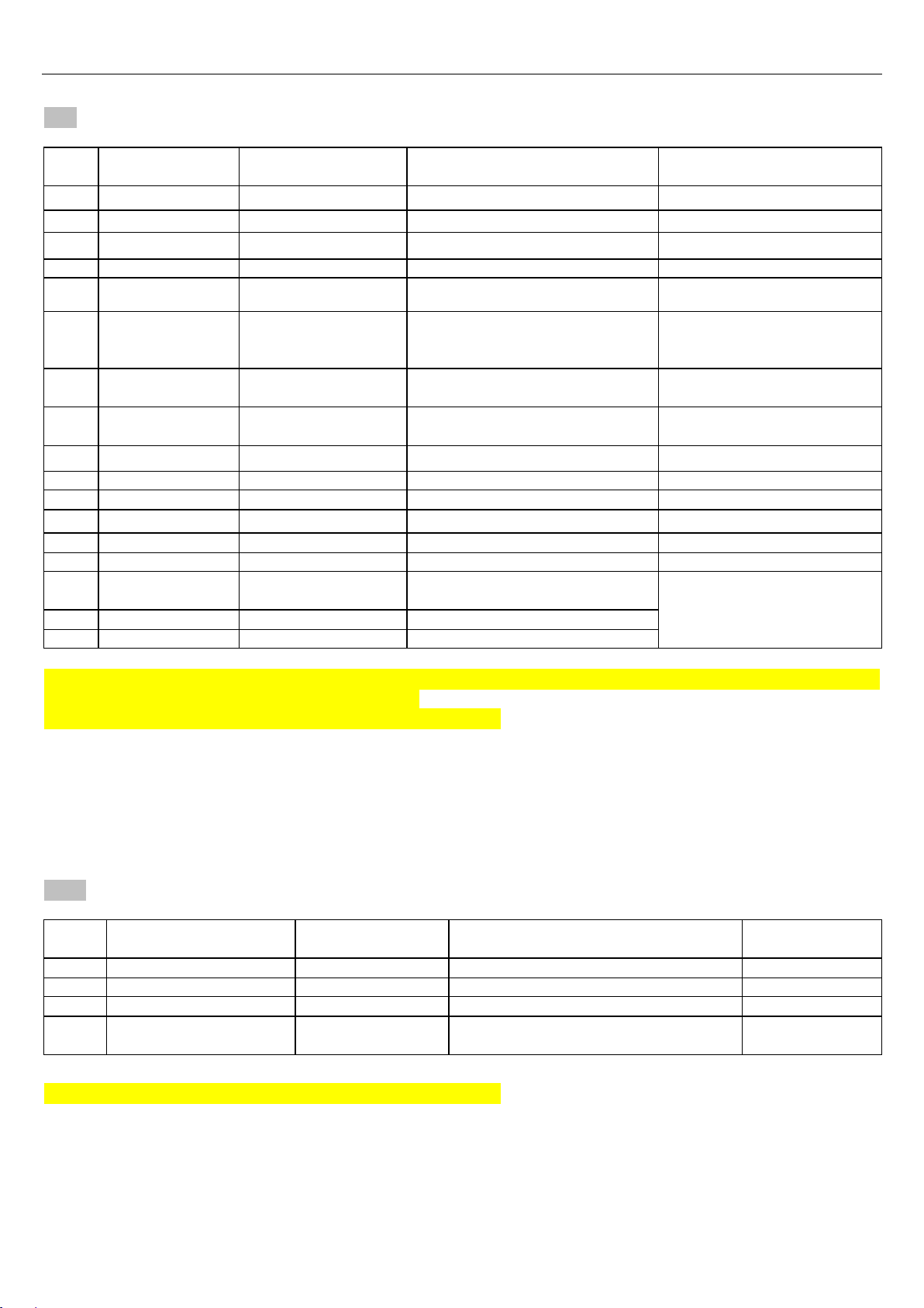
Step5、RUN POWER
Note 1:It is recommendation to check the ALLSYSPG first. If this signal is right, you can check the next step directly.
If this signal is fault, please check the related signal.
Note 2:The L > H signal is H level;The H > L signal is L level
Step6、CPU Power
Note 1:The L > H signal is H level;The H > L signal is L level
Page 14
13
4、Clock Map & Repair Flow Chart
4.1、CLOCK MAP
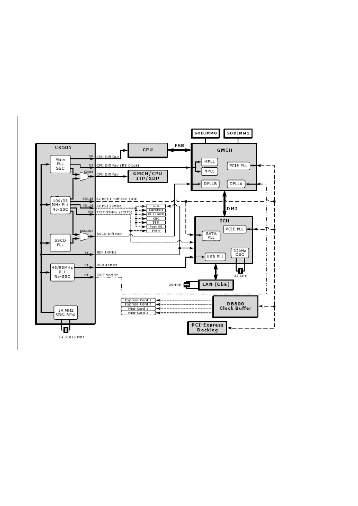
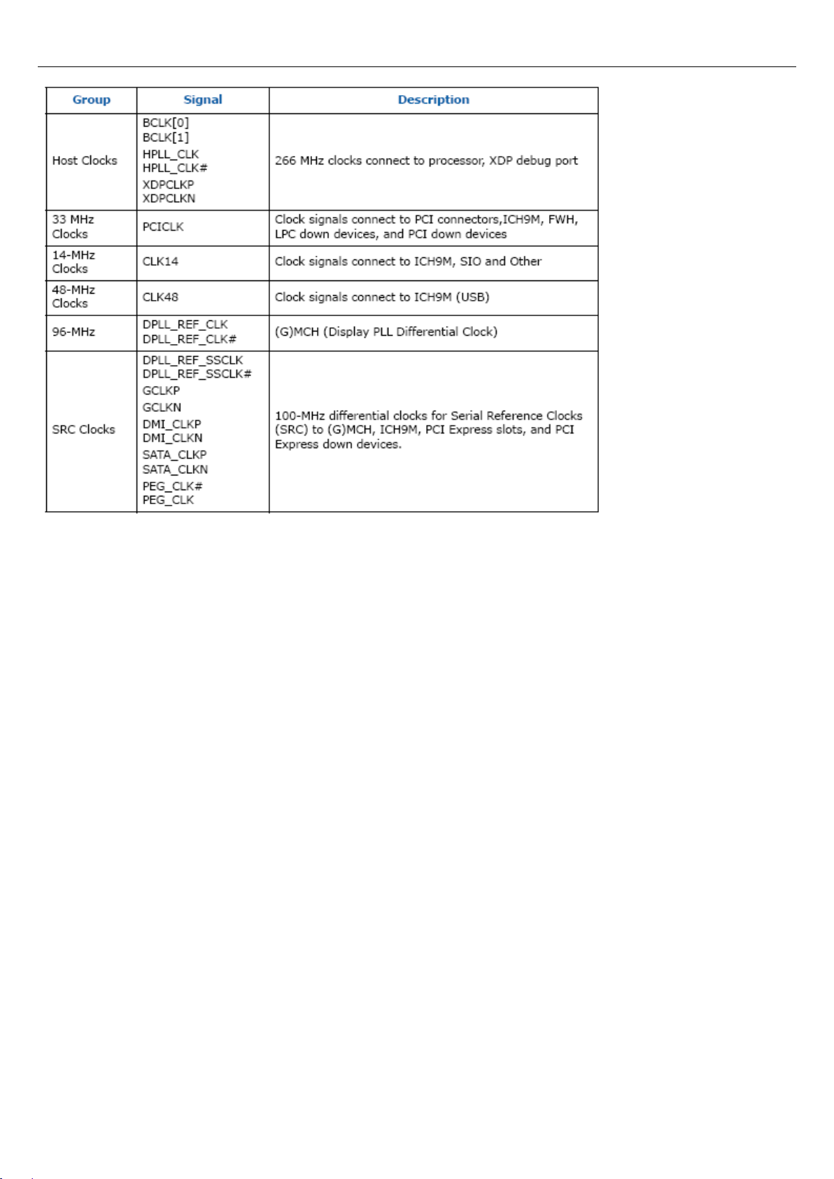
Montevina platform uses the CK505 single-chip clock solution. Figure 1 and Figure 2 show the implementation of the clocks for a
typical platform, with an internal graphics solution
Figure 1 Clock Distribution Diagram- Internal Graphics
Figure 2 (G)MCH Chipset Clock Groups
Page 15
14
Page 16
15
Item
Subject
Net name
Level
Measure Point
1
Power
+3VALW
+3.3V
U10,PIN11
2
Clock
EC_XIN
32.768KHZ
U10,PIN138
3
Clock
EC_XOUT
32.768KHZ
U10,PIN139
Item
Subject
Net name
Level
Measure Point
1
Clock
RTCX1
32.768KHZ
Y1,PIN2
2
Clock
RTCX2
32.768KHZ
Y1,PIN1
Item
Subject
Net name
Level
Measure Point
1
Clock
XTAL_IN
14.318MHZ
Y6,PIN3
2
Clock
XTAL_OUT
14.318MHZ
Y6,PIN1
Item
Subject
Net name
Level
Measure Point
1
Control Signal
CLK_PG
V
U55,PIN23
Item
Subject
Net name
Level
Measure Point
Notice
1
PCI Clocks
LPC_DEBUG
33.3MHZ
RN26,PIN6
2
PCI Clocks
PCLK_CARD
33.3MHZ
RN26,PIN8
3
PCI Clocks
LPC_EC_CLK
33.3MHZ
RN26,PIN4
4
5
SRC clocks
CLK_MINI_PCIE3
100MHZ
R734
6
SRC clocks
CLK_MINI_PCIE3#
100MHZ
R735
7
14MHZ Clocks
CLK_REF_ICH
14.318MHZ
R721
8
48MHZ Clocks
CLK_USB48
48MHZ
R719
9
Host clocks
CLK_CPU_BCLK
533 MHZ
R714
CPU_BSEL(2,1,0)=0,0,1
10
Host clocks
CLK_CPU_BCLK#
533 MHZ
R723
CPU_BSEL(2,1,0)=0,0,1
11
Host clocks
CLK_MCH_BCLK
533 MHZ
R724
CPU_BSEL(2,1,0)=0,0,1
4.2 Repair Flow
If we find all power of system is ready, we must follow below steps for checking clocks whether is correct or not.
1. Check power (+3VALW) & clock of EC whether is active or not.
2. Check RTC clock whether is active or not.
3. Check power (+3VMCLK&VDDIO_CLK) & clock of CLK Gen whether is active or not.
4. Check CLK_PWRGD whether is active or not.
5. Check clocks of all frequency whether are active or not.
Page 17
16
12
Host clocks
CLK_MCH_BCLK#
533 MHZ
R717
CPU_BSEL(2,1,0)=0,0,1
13
SRC clocks
CLK_PCIE_3GPLL#
100MHZ
R741
14
SRC clocks
CLK_PCIE_3GPLL
100MHZ
R740
15
SRC clocks
CLK_PCIE_ICH
100MHZ
R736
16
SRC clocks
CLK_PCIE_ICH#
100MHZ
R737
17
SRC clocks
CLK_MINI_PCIE1
100MHZ
R716
18
SRC clocks
CLK_MINI_PCIE1#
100MHZ
R718
19
SRC clocks
CLK_MINI_PCIE2
100MHZ
R728
20
SRC clocks
CLK_MINI_PCIE2#
100MHZ
R730
21
SRC clocks
CLK_PCIE_SATA
100MHZ
R742
22
SRC clocks
CLK_PCIE_SATA #
100MHZ
R743
Page 18

17
Page 19
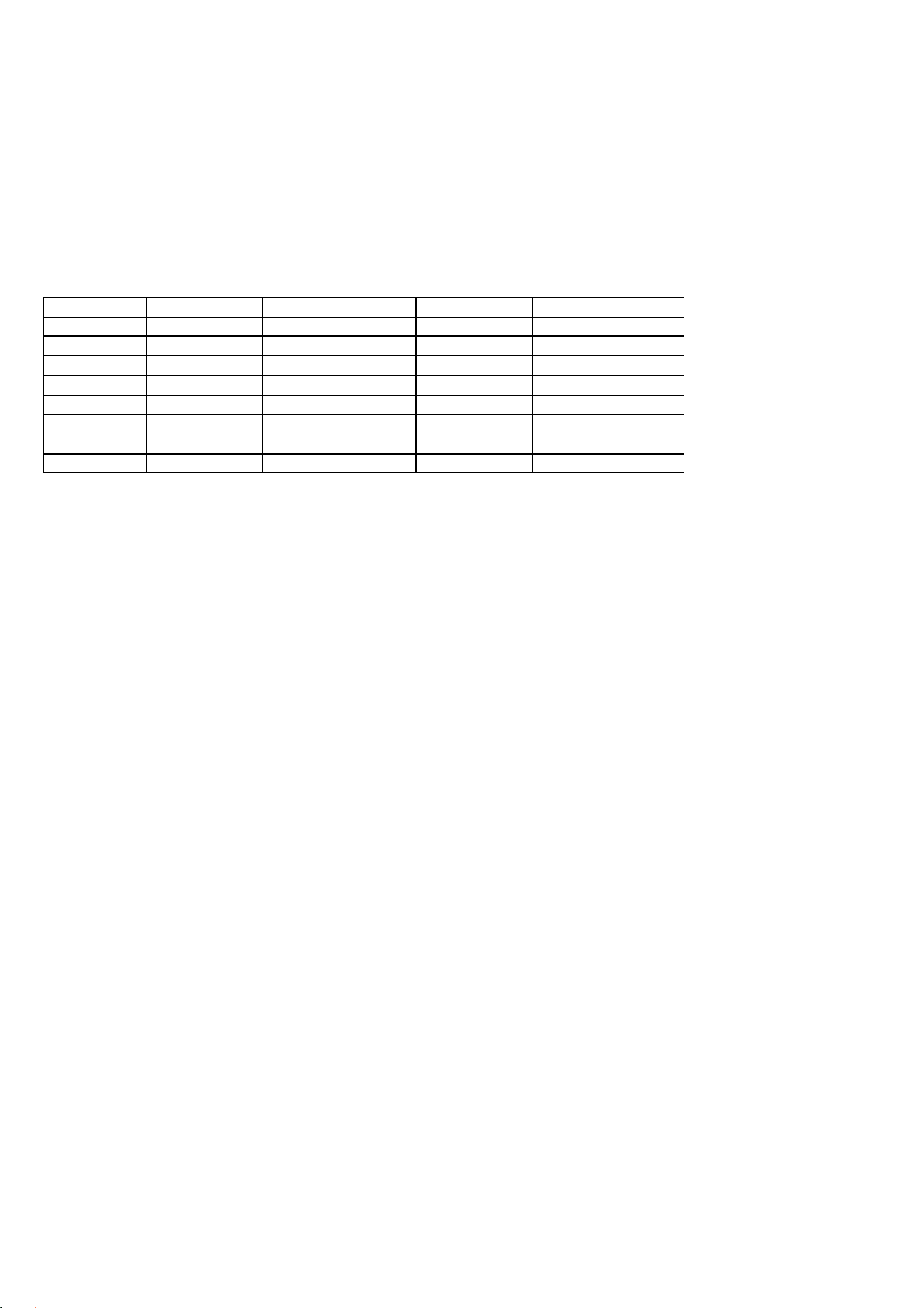
18
Item
Subject
Net name
Level
Measure Point
1
RST#
PLT_RST#
V
R835
2
RST#
LPC_RST#
V
RN23,PIN4
3
RST#
TV_RST#
V
RN16,PIN4
4
RST#
ROBSON_RST#
V
RN16,PIN2
5
RST#
NEWCARD_RST#
V
RN16,PIN6
6
RST#
MXM_RST#
V
RN23,PIN8
7
RST#
NB_RST#
V
RN23,PIN6
8
RST#
WLAN_RST#
V
RN16,PIN8
5、System Reset Map & Repair Flow Chart
If we find all power good signals of system is ready ,we must follow below steps for checking reset signals(RST#)
whether is correct or not.
1. Check PLT_RST# and RST# of other devices from SB whether is active or not.
SB(U28) schematic
Page 20

19
Item
Subject
Net name
Level
Measure Point
1
RST#
H_CPURST#
V
As below
via,U3,PIN C12
2. Check H_CPURST# for CPU whether is active or not.
CPU(U25) schematic
Page 21
20
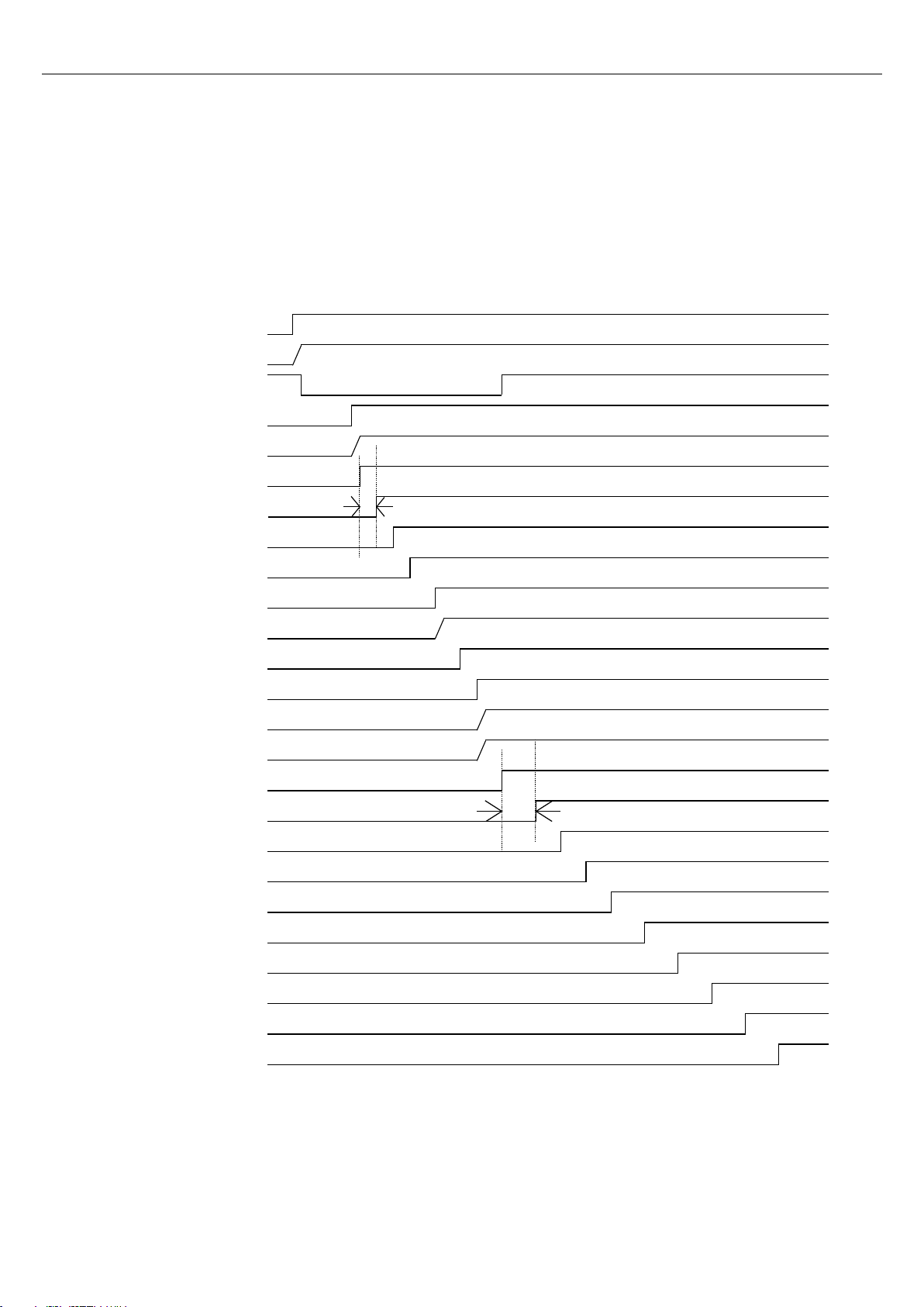
6、Power On Sequence
Power Up
H_CPURST-
>99ms
IMVP_PWRGD
CLK_PWRGD
PM_SLP_S5-
RSMRST-
+3VSUSPWROK
H_PWRGD
>=10ms
RUN_ON
1.8VDIMM/SMDDR_VTERM
DIMM_ON
PM_SLP_S3-
PM_SLP_S4-
+1_5VRUN/VTT
+3VRUN/+5VRUN
VR_ON
VR_PWRGD_CLKEN
V_CORE
SUS_ON
PCI_RST-
PLT_RST-
+3VALW/+5VALW
PWRSW-
PWR_SRC
+3VSUS/+5VSUS
ALLSYSPG
6.1 S5 S0
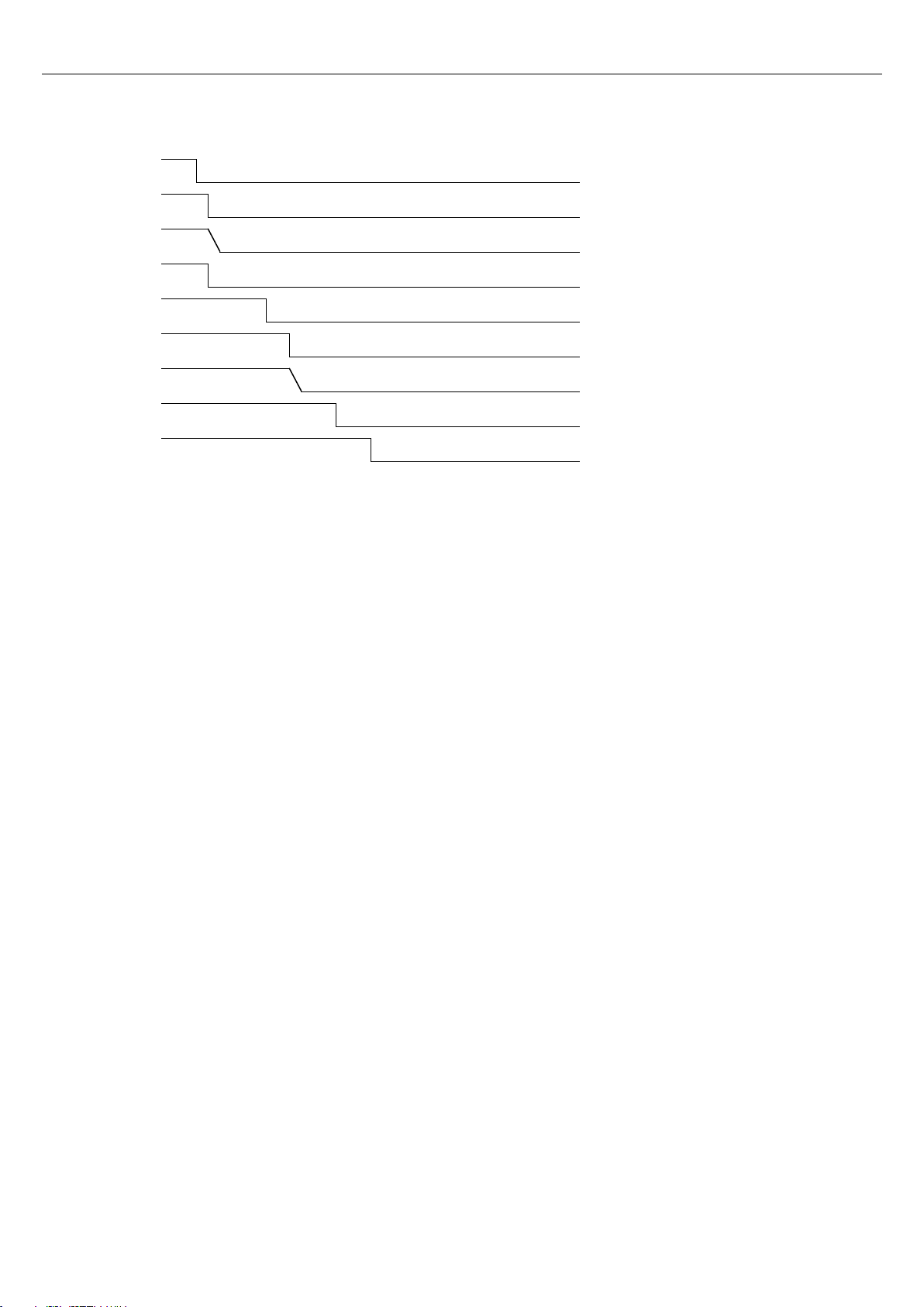
6.2 S0 S5
Page 22
21
PM_SLP_S3-
PM_SLP_S4-
VR_ON
RUN Power
RUN_ON
RSMRST-
PM_SLP_S5-
Dimm Power
DIMM_ON
Power Down
Page 23
22
Checkpoint
Description
D0
NMI is Disabled. CPU ID saved. Init code Checksum verification starting.
D1
To do DMA init, Keyboard controller BAT test, start memory refresh and going to 4GB flat mode.
D3
To start Memory sizing.
D4
To comeback to real mode. Execute OEM patch. Set stack.
D5
E000 ROM enabled. Init code is copied to segment 0 and control to be transferred to segment 0.
D6
Control is in segment 0. To check <CTRL><HOME> key and verify main BIOS checksum. If either
<CTRL><HOME> is pressed or main BIOS checksum is bad, go to check point E0 else go to check
point D7.
D7
To pass control to Interface Module.
D8
Main BIOS runtime code is to be decompressed.
D9
Control to be passed to main BIOS in shadow RAM.
Checkpoint
Meaning
E0
On Board Floppy Controller (if any) is initialized. To start base 512K memory test.
E1
To initialize interrupt vector table.
E2
To initialize DMA and interrupt controllers.
E6
To enable floppy and timer IRQ, enable internal cache.
ED
Initialize floppy drive.
EE
Start looking for a diskette in drive A: and read 1st sector of the diskette.
EF
Floppy read error.
F0
Start searching AMIBOOT.ROM file in root directory.
F1
AMIBOOT.ROM file not present in root directory.
F2
Start reading FAT table and analyze FAT to find the clusters occupied by AMIBOOT.ROM file.
F3
Start reading AMIBOOT.ROM file cluster by cluster.
F4
AMIBOOT.ROM file not of proper size.
F5
Disable internal cache.
FB
Detect Flash type present.
FC
Erase Flash.
FD
Program Flash.
FF
Flash program successful. BIOS is going to restart.
Checkpoint
Meaning
03
NMI is Disabled. To check soft reset/power-on.
05
BIOS stack set. Going to disable Cache if any.
06
POST code to be uncompressed.
07
CPU init and CPU data area init to be done.
08
CMOS checksum calculation to be done next.
0B
Any initialization before keyboard BAT to be done next.
0C
KB controller I/B free. To issue the BAT command to keyboard controller.
0E
Any initialization after KB controller BAT to be done next.
0F
Keyboard command byte to be written.
10
Going to issue Pin-23,24 blocking/unblocking command.
11
Going to check pressing of <INS> , <END> key during power-on.
12
To init CMOS if nit CMOS in every boot” is set or <END> key is pressed. Going to disable DMA and
Interrupt controllers.
13
Video display is disabled and port-B is initialized. Chipset init about to begin.
14
8254 timer test about to start.
19
About to start memory refresh test.
7、AMI BIOS Check Point list
Following is the checkpoint list in AMIBIOS in order of execution.
1.Uncompressed INIT code checkpoints
2. Boot Block Recovery Code Check Points
3.Runtime code is uncompressed in F000 shadow ram
Page 24
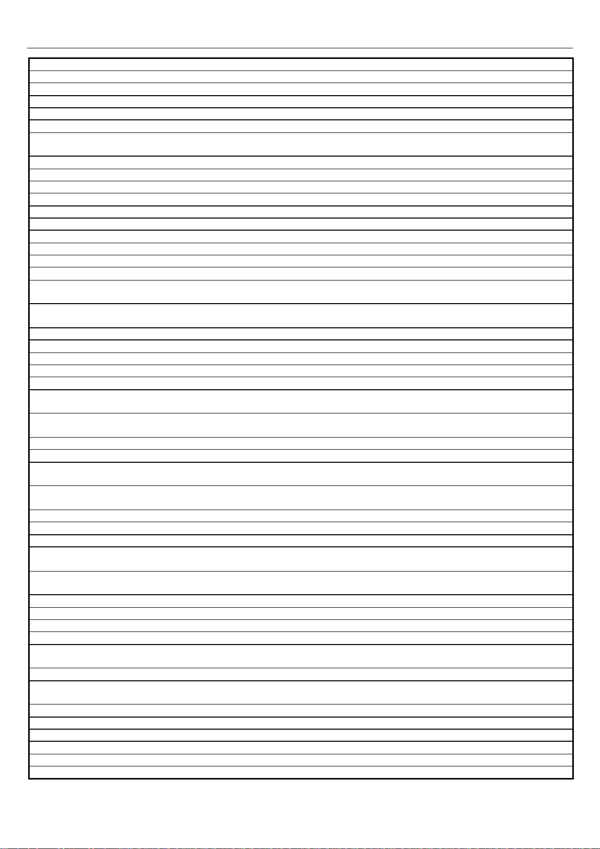
23
1A
Memory Refresh line is toggling. Going to check 15us ON/OFF time.
23
To read 8042 input port and disable Megakey Green PC feature. Make BIOS code segment writeable.
24
To do any setup before Int vector init.
25
Interrupt vector initialization about to begin. To clear password if necessary.
27
Any initialization before setting video mode to be done.
28
Going for monochrome mode and color mode setting.
2A
Different BUSes init (system, static, output devices) to start if present. (Please see Appendix for details
of different BUSes).
2B
To give control for any setup required before optional video ROM check.
2C
To look for optional video ROM and give control.
2D
To give control to do any processing after video ROM returns control.
2E
If EGA/VGA not found then do display memory R/W test.
2F
EGA/VGA not found. Display memory R/W test about to begin.
30
Display memory R/W test passed. About to look for the retrace checking.
31
Display memory R/W test or retrace checking failed. To do alternate Display memory R/W test.
32
Alternate Display memory R/W test passed. To look for the alternate display retrace checking.
34
Video display checking over. Display mode to be set next.
37
Display mode set. Going to display the power on message.
38
Different BUSes init (input, IPL, general devices) to start if present. (Please see Appendix for details of
different BUSes).
39
Display different BUSes initialization error messages. (Please see Appendix for details of different
BUSes).
3A
New cursor position read and saved. To display the Hit <DEL> message.
40
To prepare the descriptor tables.
42
To enter in virtual mode for memory test.
43
To enable interrupts for diagnostics mode.
44
To initialize data to check memory wrap around at 0:0.
45
Data initialized. Going to check for memory wrap around at 0:0 and finding the total system memory
size.
46
Memory wrap around test done. Memory size calculation over. About to go for writing patterns to test
memory.
47
Pattern to be tested written in extended memory. Going to write patterns in base 640k memory.
48
Patterns written in base memory. Going to find out amount of memory below 1M memory.
49
Amount of memory below 1M found and verified. Going to find out amount of memory above 1M
memory.
4B
Amount of memory above 1M found and verified. Check for soft reset and going to clear memory below
1M for soft reset. (If power on, go to check point# 4Eh).
4C
Memory below 1M cleared.(SOFT RESET) Going to clear memory above 1M.
4D
Memory above 1M cleared.(SOFT RESET) Going to save the memory size. (Goto check point# 52h).
4E
Memory test started. (NOT SOFT RESET) About to display the first 64k memory size.
4F
Memory size display started. This will be updated during memory test. Going for sequential and random
memory test.
50
Memory testing/initialization below 1M complete. Going to adjust displayed memory size for relocation/
shadow.
51
Memory size display adjusted due to relocation/ shadow. Memory test above 1M to follow.
52
Memory testing/initialization above 1M complete. Going to save memory size information.
53
Memory size information is saved. CPU registers are saved. Going to enter in real mode.
54
Shutdown successful, CPU in real mode. Going to disable gate A20 line and disable parity/NMI.
57
A20 address line, parity/NMI disable successful. Going to adjust memory size depending on
relocation/shadow.
58
Memory size adjusted for relocation/shadow. Going to clear Hit <DEL> message.
59
Hit <DEL> message cleared. <WAIT...> message displayed. About to start DMA and interrupt controller
test.
60
DMA page register test passed. To do DMA#1 base register test.
62
DMA#1 base register test passed. To do DMA#2 base register test.
65
DMA#2 base register test passed. To program DMA unit 1 and 2.
66
DMA unit 1 and 2 programming over. To initialize 8259 interrupt controller.
7F
Extended NMI sources enabling is in progress.
80
Keyboard test started. clearing output buffer, checking for stuck key, to issue keyboard reset command.
Page 25
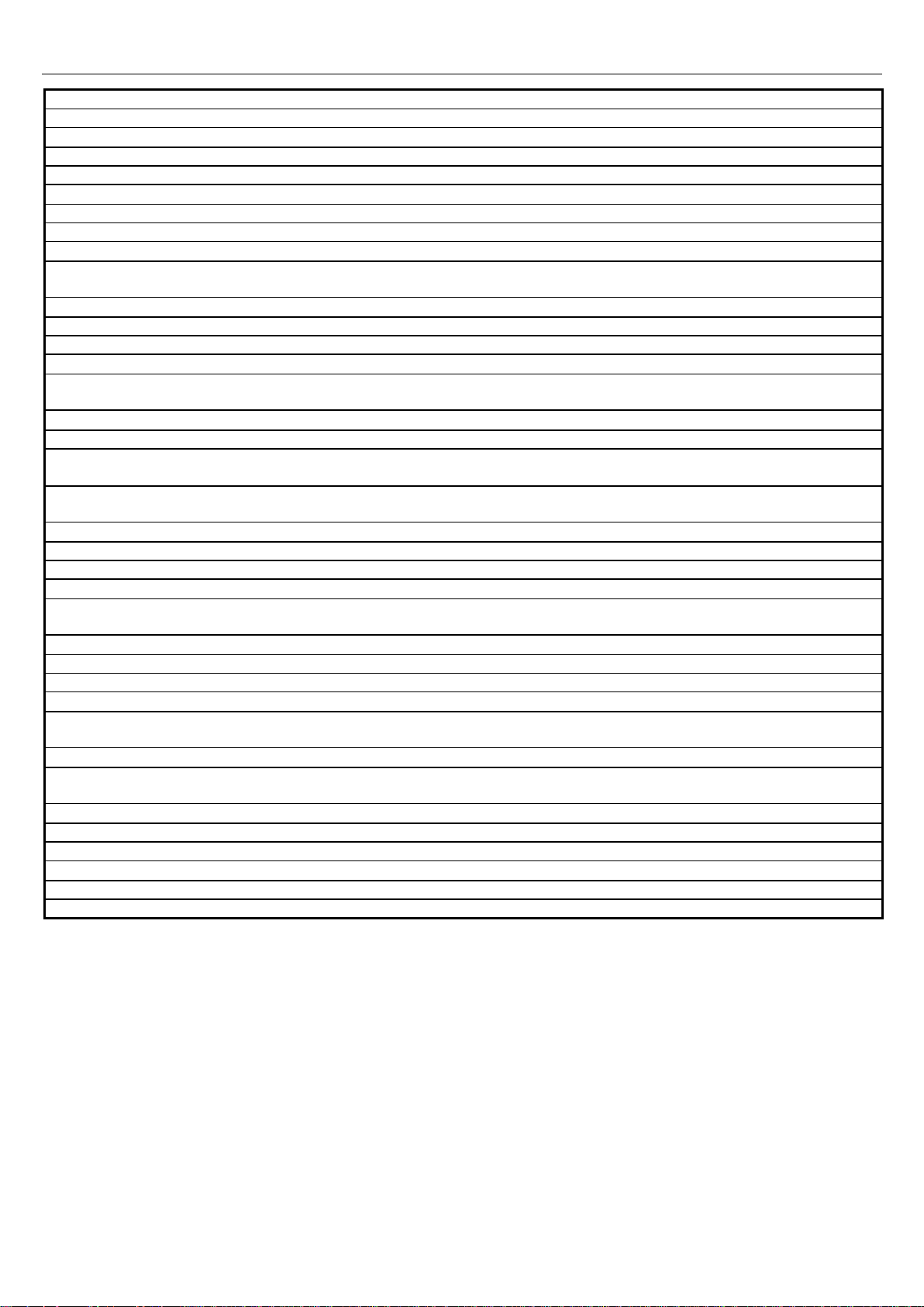
24
81
Keyboard reset error/stuck key found. To issue keyboard controller interface test command.
82
Keyboard controller interface test over. To write command byte and init circular buffer.
83
Command byte written, Global data init done. To check for lock-key.
84
Lock-key checking over. To check for memory size mismatch with CMOS.
85
Memory size check done. To display soft error and check for password or bypass setup.
86
Password checked. About to do programming before setup.
87
Programming before setup complete. To uncompress SETUP code and execute CMOS setup.
88
Returned from CMOS setup program and screen is cleared. About to do programming after setup.
89
Programming after setup complete. Going to display power on screen message.
8B
First screen message displayed. <WAIT...> message displayed. PS/2 Mouse check and extended BIOS
data area allocation to be done.
8C
Setup options programming after CMOS setup about to start.
8D
Going for hard disk controller reset.
8F
Hard disk controller reset done. Floppy setup to be done next.
91
Floppy setup complete. Hard disk setup to be done next.
95
Init of different BUSes optional ROMs from C800 to start. (Please see Appendix-I for details of different
BUSes).
96
Going to do any init before C800 optional ROM control.
97
Any init before C800 optional ROM control is over. Optional ROM check and control will be done next.
98
Optional ROM control is done. About to give control to do any required processing after optional ROM
returns control and enable external cache.
99
Any initialization required after optional ROM test over. Going to setup timer data area and printer base
address.
9A
Return after setting timer and printer base address. Going to set the RS-232 base address.
9B
Returned after RS-232 base address. Going to do any initialization before Coprocessor test.
9C
Required initialization before Coprocessor is over. Going to initialize the Coprocessor next.
9D
Coprocessor initialized. Going to do any initialization after Coprocessor test.
9E
Initialization after Coprocessor test is complete. Going to check extd keyboard, keyboard ID and
num-lock. Keyboard ID command to be
A2
Going to display any soft errors.
A3
Soft error display complete. Going to set keyboard typematic rate.
A4
Keyboard typematic rate set. To program memory wait states.
A5
Going to enable parity/NMI.
A7
NMI and parity enabled. Going to do any initialization required before giving control to optional ROM at
E000.
A8
Initialization before E000 ROM control over. E000 ROM to get control next.
A9
Returned from E000 ROM control. Going to do any initialization required after E000 optional ROM
control.
AA
Initialization after E000 optional ROM control is over. Going to display the system configuration.
AB
To build MP table if needed.
AC
To uncompress DMI data and execute DMI POST init.
B0
System configuration is displayed.
B1
Going to copy any code to specific area.
00
Copying of code to specific area done. Going to give control to INT-19 boot loader.
 Loading...