


查询M68TC08GR8FA32供应商
Freescale Semiconductor, Inc.
MC68HC908GR8
MC68HC908GR4
nc...
I
Technical Data
cale Semiconductor,
Frees
M68HC08
Microcontrollers
WWW.MOTOROLA.COM/SEMICONDUCTORS
MC68HC908GR8/D
Rev. 4, 6/2002
For More Information On This Product,
Go to: www.freescale.com

Freescale Semiconductor, Inc.
nc...
I
cale Semiconductor,
Frees
For More Information On This Product,
Go to: www.freescale.com

Freescale Semiconductor, Inc.
MC68HC908GR8
MC68HC908GR4
nc...
I
cale Semiconductor,
Frees
Technical Data — Rev 4.0
Motorola reserves the righ t to make changes without further notice to any products
herein. Motorola makes no warranty, representation or guarantee regarding the
suitability of i ts products for any partic ular purpose, nor does Moto rola assume any
liability arising out of the application or use of any prod uct or circuit, and s pecifically
disclaims any an d all liability, including withou t limitation consequential or inc idental
damages. "Typical" parameters which may be provided in Motorola data sheets and/or
specifications can an d do vary in different applications and actua l performance may
vary over time. A ll operating parameters, i ncluding "Typicals" must be validated for
each customer application by customer’s technical experts. Motorola does not convey
any license under i ts patent rights nor the rig hts of others. Motorola prod ucts are not
designed, intended, or authorized for use as components in systems intended for
surgical implant into the body, or other applications intended to support or sustain life,
or for any other applicat ion in wh ich the failure of the Mo torola pr oduct could cr eate a
situation where personal injury or death may oc cur. Should Buyer purchase o r use
Motorola products for any such unintended or una uthorized application, Buye r shall
indemnify and hold Motorola and its officers, employees, subsid iaries, affiliates, and
distributors harmless against all claims, costs, damages, and expenses, and
reasonable attorney fees arising out of, directly or indirectly, any claim of personal
injury or death associated with such unintended or unauthorized use, even if such claim
alleges that Motorola was negligent reg arding the design o r manufacture of the p art.
Motorola, Inc. is an Equal Opportunity/Affirmative Action Employer.
Motorola and are registered trademarks of Motorola, Inc.
DigitalDNA is a trademark of Motorola, Inc. © Motorola, Inc., 2002
MC68HC908GR8 — Rev 4.0 Technical Data
MOTOROLA 3
For More Information On This Product,
Go to: www.freescale.com

Freescale Semiconductor, Inc.
nc...
I
cale Semiconductor,
Frees
Technical Data MC68HC908GR8 — Rev 4.0
4 MOTOROLA
For More Information On This Product,
Go to: www.freescale.com

Freescale Semiconductor, Inc.
Technical Data — MC68HC908GR8
List of Paragraphs. . . . . . . . . . . . . . . . . . . . . . . . . . . . . . . .5
Table of Contents . . . . . . . . . . . . . . . . . . . . . . . . . . . . . . . .7
List of Tables. . . . . . . . . . . . . . . . . . . . . . . . . . . . . . . . . . .17
List of Paragraphs
nc...
I
cale Semiconductor,
Frees
List of Figures . . . . . . . . . . . . . . . . . . . . . . . . . . . . . . . . . .19
Section 1. General Description . . . . . . . . . . . . . . . . . . . .25
Section 2. Memory Map . . . . . . . . . . . . . . . . . . . . . . . . . .35
Section 3. Low Power Modes. . . . . . . . . . . . . . . . . . . . . .49
Section 4. Resets and Interrupts. . . . . . . . . . . . . . . . . . .61
Section 5. Analog-to-Digital Converter (ADC) . . . . . . . .79
Section 6. Break Module (BRK) . . . . . . . . . . . . . . . . . . . .91
Section 7. Clock Generator Module (CGMC) . . . . . . . . .99
Section 8. Configuration Register (CONFIG) . . . . . . . .129
Section 9. Computer Operating Properly (COP) . . . . .133
Section 10. Central Processing Unit (CPU) . . . . . . . . .139
Section 11. Flash Memory . . . . . . . . . . . . . . . . . . . . . . .157
Section 12. External Interrupt (IRQ) . . . . . . . . . . . . . . .167
Section 13. Keyboard Interr upt (KBI) . . . . . . . . . . . . . .175
Section 14. Low-Voltage Inhibit (LVI) . . . . . . . . . . . . . .183
Section 15. Monitor ROM (MON) . . . . . . . . . . . . . . . . . .189
Section 16. Input/Output Ports (I/O) . . . . . . . . . . . . . . .205
MC68HC908GR8 — Rev 4.0 Technical Data
MOTOROLA List of Paragraphs 5
For More Information On This Product,
Go to: www.freescale.com

List of Paragraphs
nc...
I
Freescale Semiconductor, Inc.
Section 17. RAM . . . . . . . . . . . . . . . . . . . . . . . . . . . . . . .229
Section 18. Serial Communications Interface (SCI). . .231
Section 19. System Integration Module (SIM) . . . . . . .271
Section 20. Serial Peripheral Interface (SPI). . . . . . . . .297
Section 21. Timebase Module (TBM). . . . . . . . . . . . . . .329
Section 22. Timer Interface Module (TIM). . . . . . . . . . .335
Section 23. Electrical Specificatio ns. . . . . . . . . . . . . . .361
Section 24. Mechanical Specifications . . . . . . . . . . . . .387
Section 25. Ordering Information . . . . . . . . . . . . . . . . .391
cale Semiconductor,
Frees
Glossary. . . . . . . . . . . . . . . . . . . . . . . . . . . . . . . . . . . . . .395
Revision History . . . . . . . . . . . . . . . . . . . . . . . . . . . . . . .405
Technical Data MC68HC908GR8 — Rev 4.0
6 List of Paragraphs MOTOROLA
For More Information On This Product,
Go to: www.freescale.com

Freescale Semiconductor, Inc.
Technical Data — MC68HC908GR8
Table of Contents
List of Paragraphs
Table of Contents
nc...
I
cale Semiconductor,
Frees
List of Tables
List of Figures
Section 1. General Description
1.1 Contents. . . . . . . . . . . . . . . . . . . . . . . . . . . . . . . . . . . . . . . . . .25
1.2 Introduction. . . . . . . . . . . . . . . . . . . . . . . . . . . . . . . . . . . . . . . .25
1.3 Features . . . . . . . . . . . . . . . . . . . . . . . . . . . . . . . . . . . . . . . . . .26
1.4 MCU Block Diagram. . . . . . . . . . . . . . . . . . . . . . . . . . . . . . . . .28
1.5 Pin Assignments. . . . . . . . . . . . . . . . . . . . . . . . . . . . . . . . . . . .30
1.6 Pin Functions . . . . . . . . . . . . . . . . . . . . . . . . . . . . . . . . . . . . . .31
Section 2. Memory Map
2.1 Contents. . . . . . . . . . . . . . . . . . . . . . . . . . . . . . . . . . . . . . . . . .35
2.2 Introduction. . . . . . . . . . . . . . . . . . . . . . . . . . . . . . . . . . . . . . . .35
2.3 Unimplemented Memory Locations . . . . . . . . . . . . . . . . . . . . . .35
2.4 Reserved Memory Locations . . . . . . . . . . . . . . . . . . . . . . . . . .36
2.5 Input/Output (I/O) Section. . . . . . . . . . . . . . . . . . . . . . . . . . . . .36
MC68HC908GR8 — Rev 4.0 Technical Data
MOTOROLA Table of Contents 7
For More Information On This Product,
Go to: www.freescale.com

Table of Contents
Freescale Semiconductor, Inc.
Section 3. Low Power Modes
3.1 Contents. . . . . . . . . . . . . . . . . . . . . . . . . . . . . . . . . . . . . . . . . .49
3.2 Introduction. . . . . . . . . . . . . . . . . . . . . . . . . . . . . . . . . . . . . . . .49
3.3 Analog-to-Digital Converter (ADC). . . . . . . . . . . . . . . . . . . . . .50
3.4 Break Module (BRK). . . . . . . . . . . . . . . . . . . . . . . . . . . . . . . . .51
3.5 Central Processor Unit (CPU). . . . . . . . . . . . . . . . . . . . . . . . . .51
3.6 Clock Generator Module (CGM). . . . . . . . . . . . . . . . . . . . . . . . 52
3.7 Computer Operating Properly Module (COP). . . . . . . . . . . . . .52
nc...
I
cale Semiconductor,
Frees
3.8 External Interrupt Module (IRQ) . . . . . . . . . . . . . . . . . . . . . . . .53
3.9 Keyboard Interrupt Module (KBI) . . . . . . . . . . . . . . . . . . . . . . .53
3.10 Low-Voltage Inhibit Module (LVI) . . . . . . . . . . . . . . . . . . . . . . .54
3.11 Serial Communications Interface Module (SCI) . . . . . . . . . . . .54
3.12 Serial Peripheral Interface Module (SPI) . . . . . . . . . . . . . . . . .55
3.13 Timer Interface Module (TIM1 and TIM2). . . . . . . . . . . . . . . . .55
3.14 Timebase Module (TBM) . . . . . . . . . . . . . . . . . . . . . . . . . . . . .56
3.15 Exiting Wait Mode. . . . . . . . . . . . . . . . . . . . . . . . . . . . . . . . . . .57
3.16 Exiting Stop Mode. . . . . . . . . . . . . . . . . . . . . . . . . . . . . . . . . . .58
Section 4. Resets and Interrupts
4.1 Contents. . . . . . . . . . . . . . . . . . . . . . . . . . . . . . . . . . . . . . . . . .61
4.2 Introduction. . . . . . . . . . . . . . . . . . . . . . . . . . . . . . . . . . . . . . . .61
4.3 Resets. . . . . . . . . . . . . . . . . . . . . . . . . . . . . . . . . . . . . . . . . . . .61
4.4 Interrupts. . . . . . . . . . . . . . . . . . . . . . . . . . . . . . . . . . . . . . . . . .66
Section 5. Analog-to-Digital Converter (ADC)
5.1 Contents. . . . . . . . . . . . . . . . . . . . . . . . . . . . . . . . . . . . . . . . . .79
5.2 Introduction. . . . . . . . . . . . . . . . . . . . . . . . . . . . . . . . . . . . . . . .79
Technical Data MC68HC908GR8 — Rev 4.0
8 Table of Conten ts MOTOROLA
For More Information On This Product,
Go to: www.freescale.com

Freescale Semiconductor, Inc.
5.3 Features . . . . . . . . . . . . . . . . . . . . . . . . . . . . . . . . . . . . . . . . . .80
5.4 Functional Description . . . . . . . . . . . . . . . . . . . . . . . . . . . . . . .80
5.5 Interrupts. . . . . . . . . . . . . . . . . . . . . . . . . . . . . . . . . . . . . . . . . .83
5.6 Low-Power Modes . . . . . . . . . . . . . . . . . . . . . . . . . . . . . . . . . . 83
5.7 I/O Signals . . . . . . . . . . . . . . . . . . . . . . . . . . . . . . . . . . . . . . . .83
5.8 I/O Registers. . . . . . . . . . . . . . . . . . . . . . . . . . . . . . . . . . . . . . .85
Table of Contents
Section 6. Break Module (BRK)
nc...
I
cale Semiconductor,
Frees
6.1 Contents. . . . . . . . . . . . . . . . . . . . . . . . . . . . . . . . . . . . . . . . . .91
6.2 Introduction. . . . . . . . . . . . . . . . . . . . . . . . . . . . . . . . . . . . . . . .91
6.3 Features . . . . . . . . . . . . . . . . . . . . . . . . . . . . . . . . . . . . . . . . . .91
6.4 Functional Description . . . . . . . . . . . . . . . . . . . . . . . . . . . . . . .92
6.5 Low-Power Modes . . . . . . . . . . . . . . . . . . . . . . . . . . . . . . . . . . 94
6.6 Break Module Registers. . . . . . . . . . . . . . . . . . . . . . . . . . . . . .94
Section 7. Clock Generator Module (CGMC)
7.1 Contents. . . . . . . . . . . . . . . . . . . . . . . . . . . . . . . . . . . . . . . . . .99
7.2 Introduction. . . . . . . . . . . . . . . . . . . . . . . . . . . . . . . . . . . . . . . .99
7.3 Features . . . . . . . . . . . . . . . . . . . . . . . . . . . . . . . . . . . . . . . . .100
7.4 Functional Description . . . . . . . . . . . . . . . . . . . . . . . . . . . . . .100
7.5 I/O Signals . . . . . . . . . . . . . . . . . . . . . . . . . . . . . . . . . . . . . . .112
7.6 CGMC Registers. . . . . . . . . . . . . . . . . . . . . . . . . . . . . . . . . . .114
7.7 Interrupts. . . . . . . . . . . . . . . . . . . . . . . . . . . . . . . . . . . . . . . . .123
7.8 Special Modes . . . . . . . . . . . . . . . . . . . . . . . . . . . . . . . . . . . .123
7.9 Acquisition/Lock Time Specifications . . . . . . . . . . . . . . . . . . .125
MC68HC908GR8 — Rev 4.0 Technical Data
MOTOROLA Table of Contents 9
For More Information On This Product,
Go to: www.freescale.com

Table of Contents
Freescale Semiconductor, Inc.
Section 8. Configuration Register (CONFIG)
8.1 Contents. . . . . . . . . . . . . . . . . . . . . . . . . . . . . . . . . . . . . . . . .129
8.2 Introduction. . . . . . . . . . . . . . . . . . . . . . . . . . . . . . . . . . . . . . .129
8.3 Functional Description . . . . . . . . . . . . . . . . . . . . . . . . . . . . . .129
Section 9. Computer Operating Properly (COP)
9.1 Contents. . . . . . . . . . . . . . . . . . . . . . . . . . . . . . . . . . . . . . . . .133
9.2 Introduction. . . . . . . . . . . . . . . . . . . . . . . . . . . . . . . . . . . . . . .133
nc...
I
cale Semiconductor,
Frees
9.3 Functional Description . . . . . . . . . . . . . . . . . . . . . . . . . . . . . .133
9.4 I/O Signals . . . . . . . . . . . . . . . . . . . . . . . . . . . . . . . . . . . . . . .135
9.5 COP Control Register. . . . . . . . . . . . . . . . . . . . . . . . . . . . . . .136
9.6 Interrupts. . . . . . . . . . . . . . . . . . . . . . . . . . . . . . . . . . . . . . . . .136
9.7 Monitor Mode . . . . . . . . . . . . . . . . . . . . . . . . . . . . . . . . . . . . .137
9.8 Low-Power Modes . . . . . . . . . . . . . . . . . . . . . . . . . . . . . . . . . 1 37
9.9 COP Module During Break Mode. . . . . . . . . . . . . . . . . . . . . .137
Section 10. Central Processing Unit (CPU)
10.1 Contents . . . . . . . . . . . . . . . . . . . . . . . . . . . . . . . . . . . . . . . . .1 39
10.2 Introduction. . . . . . . . . . . . . . . . . . . . . . . . . . . . . . . . . . . . . . .139
10.3 Features . . . . . . . . . . . . . . . . . . . . . . . . . . . . . . . . . . . . . . . . .139
10.4 CPU registers . . . . . . . . . . . . . . . . . . . . . . . . . . . . . . . . . . . . .140
10.5 Arithmetic/logic unit (ALU) . . . . . . . . . . . . . . . . . . . . . . . . . . .145
10.6 Low-power modes . . . . . . . . . . . . . . . . . . . . . . . . . . . . . . . . .145
10.7 CPU during break interrupts. . . . . . . . . . . . . . . . . . . . . . . . . .146
10.8 Instruction Set Summary . . . . . . . . . . . . . . . . . . . . . . . . . . . .147
10.9 Opcode Map. . . . . . . . . . . . . . . . . . . . . . . . . . . . . . . . . . . . . .154
Technical Data MC68HC908GR8 — Rev 4.0
10 Table of Contents MOTOROLA
For More Information On This Product,
Go to: www.freescale.com

Freescale Semiconductor, Inc.
Table of Contents
Section 11. Flash Memory
11.1 Contents . . . . . . . . . . . . . . . . . . . . . . . . . . . . . . . . . . . . . . . . .1 57
11.2 Introduction. . . . . . . . . . . . . . . . . . . . . . . . . . . . . . . . . . . . . . .157
11.3 Functional Description . . . . . . . . . . . . . . . . . . . . . . . . . . . . . .157
11.4 FLASH Control Register. . . . . . . . . . . . . . . . . . . . . . . . . . . . .159
11.5 FLASH Page Erase Operation . . . . . . . . . . . . . . . . . . . . . . . .160
11.6 FLASH Mass Erase Operation. . . . . . . . . . . . . . . . . . . . . . . .161
11.7 FLASH Program/Read Operation. . . . . . . . . . . . . . . . . . . . . .162
nc...
I
cale Semiconductor,
Frees
11.8 FLASH Block Protection. . . . . . . . . . . . . . . . . . . . . . . . . . . . .163
11.9 Wait Mode. . . . . . . . . . . . . . . . . . . . . . . . . . . . . . . . . . . . . . . .166
11.10 STOP Mode . . . . . . . . . . . . . . . . . . . . . . . . . . . . . . . . . . . . . .166
Section 12. External Interrupt (IRQ)
12.1 Contents . . . . . . . . . . . . . . . . . . . . . . . . . . . . . . . . . . . . . . . . .1 67
12.2 Introduction. . . . . . . . . . . . . . . . . . . . . . . . . . . . . . . . . . . . . . .167
12.3 Features . . . . . . . . . . . . . . . . . . . . . . . . . . . . . . . . . . . . . . . . .167
12.4 Functional Description . . . . . . . . . . . . . . . . . . . . . . . . . . . . . .168
12.5 IRQ1 Pin. . . . . . . . . . . . . . . . . . . . . . . . . . . . . . . . . . . . . . . . .170
12.6 IRQ Module During Break Interrupts . . . . . . . . . . . . . . . . . . .1 71
12.7 IRQ Status and Control Register . . . . . . . . . . . . . . . . . . . . . .172
Section 13. Keyboard Interrupt (KBI)
13.1 Contents . . . . . . . . . . . . . . . . . . . . . . . . . . . . . . . . . . . . . . . . .1 75
13.2 Introduction. . . . . . . . . . . . . . . . . . . . . . . . . . . . . . . . . . . . . . .175
13.3 Features . . . . . . . . . . . . . . . . . . . . . . . . . . . . . . . . . . . . . . . . .175
13.4 Functional Description . . . . . . . . . . . . . . . . . . . . . . . . . . . . . .176
13.5 Keyboard Initialization. . . . . . . . . . . . . . . . . . . . . . . . . . . . . . .179
MC68HC908GR8 — Rev 4.0 Technical Data
MOTOROLA Table of Contents 11
For More Information On This Product,
Go to: www.freescale.com

Table of Contents
Freescale Semiconductor, Inc.
13.6 Low-Power Modes . . . . . . . . . . . . . . . . . . . . . . . . . . . . . . . . .1 80
13.7 Keyboard Module During Break Interrupts . . . . . . . . . . . . . . . 1 80
13.8 I/O Registers. . . . . . . . . . . . . . . . . . . . . . . . . . . . . . . . . . . . . .181
Section 14. Low-Voltage Inhibit (LVI)
14.1 Contents . . . . . . . . . . . . . . . . . . . . . . . . . . . . . . . . . . . . . . . . .1 83
14.2 Introduction. . . . . . . . . . . . . . . . . . . . . . . . . . . . . . . . . . . . . . .183
14.3 Features . . . . . . . . . . . . . . . . . . . . . . . . . . . . . . . . . . . . . . . . .183
nc...
I
cale Semiconductor,
Frees
14.4 Functional Description . . . . . . . . . . . . . . . . . . . . . . . . . . . . . .184
14.5 LVI Status Register. . . . . . . . . . . . . . . . . . . . . . . . . . . . . . . . .187
14.6 LVI Interrupts . . . . . . . . . . . . . . . . . . . . . . . . . . . . . . . . . . . . .188
14.7 Low-Power Modes . . . . . . . . . . . . . . . . . . . . . . . . . . . . . . . . .1 88
15.1 Contents . . . . . . . . . . . . . . . . . . . . . . . . . . . . . . . . . . . . . . . . .1 89
15.2 Introduction. . . . . . . . . . . . . . . . . . . . . . . . . . . . . . . . . . . . . . .189
15.3 Features . . . . . . . . . . . . . . . . . . . . . . . . . . . . . . . . . . . . . . . . .189
15.4 Functional Description . . . . . . . . . . . . . . . . . . . . . . . . . . . . . .190
15.5 Security. . . . . . . . . . . . . . . . . . . . . . . . . . . . . . . . . . . . . . . . . .202
Section 15. Monitor ROM (MON)
Section 16. Input/Output Ports (I/O)
16.1 Contents . . . . . . . . . . . . . . . . . . . . . . . . . . . . . . . . . . . . . . . . .2 05
16.2 Introduction. . . . . . . . . . . . . . . . . . . . . . . . . . . . . . . . . . . . . . .205
16.3 Port A . . . . . . . . . . . . . . . . . . . . . . . . . . . . . . . . . . . . . . . . . . .209
16.4 Port B . . . . . . . . . . . . . . . . . . . . . . . . . . . . . . . . . . . . . . . . . . .213
16.5 Port C . . . . . . . . . . . . . . . . . . . . . . . . . . . . . . . . . . . . . . . . . . .216
16.6 Port D . . . . . . . . . . . . . . . . . . . . . . . . . . . . . . . . . . . . . . . . . . .220
Technical Data MC68HC908GR8 — Rev 4.0
12 Table of Contents MOTOROLA
For More Information On This Product,
Go to: www.freescale.com

Freescale Semiconductor, Inc.
16.7 Port E . . . . . . . . . . . . . . . . . . . . . . . . . . . . . . . . . . . . . . . . . . .225
Table of Contents
Section 17. RAM
17.1 Contents . . . . . . . . . . . . . . . . . . . . . . . . . . . . . . . . . . . . . . . . .2 29
17.2 Introduction. . . . . . . . . . . . . . . . . . . . . . . . . . . . . . . . . . . . . . .229
17.3 Functional Description . . . . . . . . . . . . . . . . . . . . . . . . . . . . . .229
Section 18. Serial Communications Interface (SCI)
18.1 Contents . . . . . . . . . . . . . . . . . . . . . . . . . . . . . . . . . . . . . . . . .2 31
nc...
I
cale Semiconductor,
Frees
18.2 Introduction. . . . . . . . . . . . . . . . . . . . . . . . . . . . . . . . . . . . . . .231
18.3 Features . . . . . . . . . . . . . . . . . . . . . . . . . . . . . . . . . . . . . . . . .232
18.4 Pin Name Conventions. . . . . . . . . . . . . . . . . . . . . . . . . . . . . .233
18.5 Functional Description . . . . . . . . . . . . . . . . . . . . . . . . . . . . . .233
18.6 Low-Power Modes . . . . . . . . . . . . . . . . . . . . . . . . . . . . . . . . .2 50
18.7 SCI During Break Module Interrupts. . . . . . . . . . . . . . . . . . . .251
18.8 I/O Signals . . . . . . . . . . . . . . . . . . . . . . . . . . . . . . . . . . . . . . .251
18.9 I/O Registers. . . . . . . . . . . . . . . . . . . . . . . . . . . . . . . . . . . . . .252
Section 19. System Integration Module (SIM)
19.1 Contents . . . . . . . . . . . . . . . . . . . . . . . . . . . . . . . . . . . . . . . . .2 71
19.2 Introduction. . . . . . . . . . . . . . . . . . . . . . . . . . . . . . . . . . . . . . .271
19.3 SIM Bus Clock Control and Generation . . . . . . . . . . . . . . . . .275
19.4 Reset and System Initialization. . . . . . . . . . . . . . . . . . . . . . . .276
19.5 SIM Counter . . . . . . . . . . . . . . . . . . . . . . . . . . . . . . . . . . . . . .281
19.6 Exception Control. . . . . . . . . . . . . . . . . . . . . . . . . . . . . . . . . .282
19.7 Low-Power Modes . . . . . . . . . . . . . . . . . . . . . . . . . . . . . . . . .2 90
19.8 SIM Registers. . . . . . . . . . . . . . . . . . . . . . . . . . . . . . . . . . . . .293
MC68HC908GR8 — Rev 4.0 Technical Data
MOTOROLA Table of Contents 13
For More Information On This Product,
Go to: www.freescale.com

Table of Contents
Freescale Semiconductor, Inc.
Section 20. Serial Peripheral Interface (SPI)
20.1 Contents . . . . . . . . . . . . . . . . . . . . . . . . . . . . . . . . . . . . . . . . .2 97
20.2 Introduction. . . . . . . . . . . . . . . . . . . . . . . . . . . . . . . . . . . . . . .297
20.3 Features . . . . . . . . . . . . . . . . . . . . . . . . . . . . . . . . . . . . . . . . .298
20.4 Pin Name Conventions and I/O Register Addresses . . . . . . .298
20.5 Functional Description . . . . . . . . . . . . . . . . . . . . . . . . . . . . . .299
20.6 Transmission Formats . . . . . . . . . . . . . . . . . . . . . . . . . . . . . .303
20.7 Queuing Transmission Data. . . . . . . . . . . . . . . . . . . . . . . . . .309
nc...
I
cale Semiconductor,
Frees
20.8 Error Conditions . . . . . . . . . . . . . . . . . . . . . . . . . . . . . . . . . . .310
20.9 Interrupts. . . . . . . . . . . . . . . . . . . . . . . . . . . . . . . . . . . . . . . . .314
20.10 Resetting the SPI . . . . . . . . . . . . . . . . . . . . . . . . . . . . . . . . . .316
20.11 Low-Power Modes . . . . . . . . . . . . . . . . . . . . . . . . . . . . . . . . . 3 17
20.12 SPI During Break Interrupts . . . . . . . . . . . . . . . . . . . . . . . . . . 3 18
20.13 I/O Signals . . . . . . . . . . . . . . . . . . . . . . . . . . . . . . . . . . . . . . .318
20.14 I/O Registers. . . . . . . . . . . . . . . . . . . . . . . . . . . . . . . . . . . . . .322
Section 21. Timebase Module (TBM)
21.1 Contents . . . . . . . . . . . . . . . . . . . . . . . . . . . . . . . . . . . . . . . . .3 29
21.2 Introduction. . . . . . . . . . . . . . . . . . . . . . . . . . . . . . . . . . . . . . .329
21.3 Features . . . . . . . . . . . . . . . . . . . . . . . . . . . . . . . . . . . . . . . . .329
21.4 Functional Description . . . . . . . . . . . . . . . . . . . . . . . . . . . . . .330
21.5 Timebase Register Description. . . . . . . . . . . . . . . . . . . . . . . .331
21.6 Interrupts. . . . . . . . . . . . . . . . . . . . . . . . . . . . . . . . . . . . . . . . .332
21.7 Low-Power Modes . . . . . . . . . . . . . . . . . . . . . . . . . . . . . . . . .3 33
Section 22. Timer Interface Module (TIM)
22.1 Contents . . . . . . . . . . . . . . . . . . . . . . . . . . . . . . . . . . . . . . . . .3 35
Technical Data MC68HC908GR8 — Rev 4.0
14 Table of Contents MOTOROLA
For More Information On This Product,
Go to: www.freescale.com

Freescale Semiconductor, Inc.
22.2 Introduction. . . . . . . . . . . . . . . . . . . . . . . . . . . . . . . . . . . . . . .335
22.3 Features . . . . . . . . . . . . . . . . . . . . . . . . . . . . . . . . . . . . . . . . .336
22.4 Pin Name Conventions. . . . . . . . . . . . . . . . . . . . . . . . . . . . . .336
22.5 Functional Description . . . . . . . . . . . . . . . . . . . . . . . . . . . . . .337
22.6 Interrupts. . . . . . . . . . . . . . . . . . . . . . . . . . . . . . . . . . . . . . . . .346
22.7 Low-Power Modes . . . . . . . . . . . . . . . . . . . . . . . . . . . . . . . . .3 47
22.8 TIM During Break Interrupts. . . . . . . . . . . . . . . . . . . . . . . . . .348
22.9 I/O Signals . . . . . . . . . . . . . . . . . . . . . . . . . . . . . . . . . . . . . . .348
Table of Contents
nc...
I
cale Semiconductor,
Frees
22.10 I/O Registers. . . . . . . . . . . . . . . . . . . . . . . . . . . . . . . . . . . . . .349
Section 23. Electrical Specifications
23.1 Contents . . . . . . . . . . . . . . . . . . . . . . . . . . . . . . . . . . . . . . . . .3 61
23.2 Absolute Maximum Ratings . . . . . . . . . . . . . . . . . . . . . . . . . .362
23.3 Functional Operating Range. . . . . . . . . . . . . . . . . . . . . . . . . .363
23.4 Thermal Characteristics . . . . . . . . . . . . . . . . . . . . . . . . . . . . .363
23.5 5.0 V DC Electrical Characteristics. . . . . . . . . . . . . . . . . . . . .364
23.6 3.0 V DC Electrical Characteristics. . . . . . . . . . . . . . . . . . . . .366
23.7 5.0 V Control Timing. . . . . . . . . . . . . . . . . . . . . . . . . . . . . . . .368
23.8 3.0 V Control Timing. . . . . . . . . . . . . . . . . . . . . . . . . . . . . . . .369
23.9 Output High-Voltage Characteristics . . . . . . . . . . . . . . . . . . .370
23.10 Output Low-Voltage Characteristics. . . . . . . . . . . . . . . . . . . .373
23.11 Typical Supply Currents . . . . . . . . . . . . . . . . . . . . . . . . . . . . .376
23.12 ADC Characteristics. . . . . . . . . . . . . . . . . . . . . . . . . . . . . . . .378
23.13 5.0 V SPI Characteristics . . . . . . . . . . . . . . . . . . . . . . . . . . . . 3 79
23.14 3.0 V SPI Characteristics . . . . . . . . . . . . . . . . . . . . . . . . . . . . 3 80
23.15 Timer Interface Module Characteristics . . . . . . . . . . . . . . . . .383
MC68HC908GR8 — Rev 4.0 Technical Data
MOTOROLA Table of Contents 15
For More Information On This Product,
Go to: www.freescale.com

Table of Contents
Freescale Semiconductor, Inc.
23.16 Clock Generation Module Characteristics . . . . . . . . . . . . . . .383
23.17 Memory Characteristics . . . . . . . . . . . . . . . . . . . . . . . . . . . . .385
Section 24. Mechanical Specifications
24.1 Contents . . . . . . . . . . . . . . . . . . . . . . . . . . . . . . . . . . . . . . . . .3 87
24.2 Introduction. . . . . . . . . . . . . . . . . . . . . . . . . . . . . . . . . . . . . . .387
24.3 32-Pin LQFP (Case #873A) . . . . . . . . . . . . . . . . . . . . . . . . . .388
24.4 28-Pin PDIP (Case #710). . . . . . . . . . . . . . . . . . . . . . . . . . . .389
nc...
I
cale Semiconductor,
Frees
24.5 28-Pin SOIC (Case #751F). . . . . . . . . . . . . . . . . . . . . . . . . . .390
Section 25. Ordering Information
25.1 Contents . . . . . . . . . . . . . . . . . . . . . . . . . . . . . . . . . . . . . . . . .3 91
25.2 Introduction. . . . . . . . . . . . . . . . . . . . . . . . . . . . . . . . . . . . . . .391
25.3 MC Order Numbers . . . . . . . . . . . . . . . . . . . . . . . . . . . . . . . .392
25.4 Development Tools. . . . . . . . . . . . . . . . . . . . . . . . . . . . . . . . .393
Glossary
Revision History
Contents . . . . . . . . . . . . . . . . . . . . . . . . . . . . . . . . . . . . . . . . .4 05
Introduction. . . . . . . . . . . . . . . . . . . . . . . . . . . . . . . . . . . . . . .405
Changes from Rev 3.0 published in February 2002 to Rev 4.0
published in June 2002. . . . . . . . . . . . . . . . . . . . . . . . . . . . . .405
Changes from Rev 2.0 published in Janu ary 2002 to Rev 3.0 pub-
lished in February 2002 . . . . . . . . . . . . . . . . . . . . . . . . . . . . .406
Changes from Rev 1.0 published in April 2001 to Rev 2.0 pub-
lished in December 2001 . . . . . . . . . . . . . . . . . . . . . . . . . . . .406
Technical Data MC68HC908GR8 — Rev 4.0
16 Table of Contents MOTOROLA
For More Information On This Product,
Go to: www.freescale.com

Freescale Semiconductor, Inc.
Technical Data — MC68HC908GR8
Table Title Page
2-1 Vector Addresses. . . . . . . . . . . . . . . . . . . . . . . . . . . . . . . . . . .47
4-1 Interrupt Sources . . . . . . . . . . . . . . . . . . . . . . . . . . . . . . . . . . .70
4-2 Interrupt Source Flags . . . . . . . . . . . . . . . . . . . . . . . . . . . . . . .75
nc...
I
cale Semiconductor,
Frees
5-1 Mux Channel Select . . . . . . . . . . . . . . . . . . . . . . . . . . . . . . . . .86
5-2 ADC Clock Divide Ratio . . . . . . . . . . . . . . . . . . . . . . . . . . . . . .88
7-1 Numeric Example . . . . . . . . . . . . . . . . . . . . . . . . . . . . . . . . . .109
7-2 PRE 1 and PRE0 Programming. . . . . . . . . . . . . . . . . . . . . . .117
7-3 VPR1 and VPR0 Programming . . . . . . . . . . . . . . . . . . . . . . .117
10-1 Instruction Set Summary . . . . . . . . . . . . . . . . . . . . . . . . . . . .147
10-2 Opcode Map. . . . . . . . . . . . . . . . . . . . . . . . . . . . . . . . . . . . . .155
11-1 Examples of protect start address:. . . . . . . . . . . . . . . . . . . . .166
14-1 LVIOUT Bit Indication. . . . . . . . . . . . . . . . . . . . . . . . . . . . . . .187
15-1 Monitor Mode Signal Requirements and Options. . . . . . . . . .193
15-2 Mode Differences . . . . . . . . . . . . . . . . . . . . . . . . . . . . . . . . . .196
15-3 Monitor Baud Rate Selection . . . . . . . . . . . . . . . . . . . . . . . . .197
15-4 READ (Read Memory) Command . . . . . . . . . . . . . . . . . . . . .199
15-5 WRITE (Write Memory) Command. . . . . . . . . . . . . . . . . . . . .199
15-6 IREAD (Indexed Read) Command. . . . . . . . . . . . . . . . . . . . .200
15-7 IWRITE (Indexed Write) Command . . . . . . . . . . . . . . . . . . . .200
15-8 READSP (Read Stack Pointer) Command. . . . . . . . . . . . . . .201
15-9 RUN (Run User Program) Command. . . . . . . . . . . . . . . . . . .201
16-1 Port Control Register Bits Summary. . . . . . . . . . . . . . . . . . . .208
16-2 Port A Pin Functions. . . . . . . . . . . . . . . . . . . . . . . . . . . . . . . .211
16-3 Port B Pin Functions. . . . . . . . . . . . . . . . . . . . . . . . . . . . . . . .215
16-4 Port C Pin Functions. . . . . . . . . . . . . . . . . . . . . . . . . . . . . . . .218
16-5 Port D Pin Functions. . . . . . . . . . . . . . . . . . . . . . . . . . . . . . . .223
16-6 Port E Pin Functions. . . . . . . . . . . . . . . . . . . . . . . . . . . . . . . .227
18-1 Pin Name Conventions. . . . . . . . . . . . . . . . . . . . . . . . . . . . . .233
18-2 Start Bit Verification . . . . . . . . . . . . . . . . . . . . . . . . . . . . . . . .244
List of Tables
MC68HC908GR8 — Rev 4.0 Technical Data
MOTOROLA List of Tables 17
For More Information On This Product,
Go to: www.freescale.com

List of Tables
nc...
I
cale Semiconductor,
Frees
Freescale Semiconductor, Inc.
18-3 Data Bit Recovery . . . . . . . . . . . . . . . . . . . . . . . . . . . . . . . . . .244
18-4 Stop Bit Recovery. . . . . . . . . . . . . . . . . . . . . . . . . . . . . . . . . .245
18-5 Character Format Selection . . . . . . . . . . . . . . . . . . . . . . . . . .255
18-6 SCI Baud Rate Prescaling . . . . . . . . . . . . . . . . . . . . . . . . . . .266
18-7 SCI Baud Rate Selection . . . . . . . . . . . . . . . . . . . . . . . . . . . .266
18-8 SCI Baud Rate Selection Examples. . . . . . . . . . . . . . . . . . . .268
19-1 Signal Name Conventions . . . . . . . . . . . . . . . . . . . . . . . . . . .273
19-2 PIN Bit Set Timing . . . . . . . . . . . . . . . . . . . . . . . . . . . . . . . . .277
19-3 Interrupt Sources . . . . . . . . . . . . . . . . . . . . . . . . . . . . . . . . . .286
19-4 SIM Registers. . . . . . . . . . . . . . . . . . . . . . . . . . . . . . . . . . . . . 2 93
20-1 Pin Name Conventions. . . . . . . . . . . . . . . . . . . . . . . . . . . . . .299
20-2 SPI Interrupts . . . . . . . . . . . . . . . . . . . . . . . . . . . . . . . . . . . . .314
20-3 SPI Configuration . . . . . . . . . . . . . . . . . . . . . . . . . . . . . . . . . .321
20-4 SPI Master Baud Rate Selection . . . . . . . . . . . . . . . . . . . . . .327
21-1 Timebase Rate Selection for OSC1 = 32.768 kHz. . . . . . . . .331
22-1 Pin Name Conventions. . . . . . . . . . . . . . . . . . . . . . . . . . . . . .336
22-2 Prescaler Selection. . . . . . . . . . . . . . . . . . . . . . . . . . . . . . . . .351
22-3 Mode, Edge, and Level Selection. . . . . . . . . . . . . . . . . . . . . .358
23-1 Absolute Maximum Ratings . . . . . . . . . . . . . . . . . . . . . . . . . .362
23-2 Functional Operation Range. . . . . . . . . . . . . . . . . . . . . . . . . .363
23-3 Thermal Characteristics . . . . . . . . . . . . . . . . . . . . . . . . . . . . .363
23-4 5.0V DC Electrical Characteristics . . . . . . . . . . . . . . . . . . . . .364
23-5 3.0 V DC Electrical Characteristics. . . . . . . . . . . . . . . . . . . . .366
23-6 5.0 V Control Timing. . . . . . . . . . . . . . . . . . . . . . . . . . . . . . . .368
23-7 3.0 V Control Timing. . . . . . . . . . . . . . . . . . . . . . . . . . . . . . . .369
23-8 Timer Interface Module Characteristics . . . . . . . . . . . . . . . . .383
23-9 CGM Component Specifications. . . . . . . . . . . . . . . . . . . . . . .383
25-1 MC Order Numbers . . . . . . . . . . . . . . . . . . . . . . . . . . . . . . . .392
25-2 Development Tool Kits . . . . . . . . . . . . . . . . . . . . . . . . . . . . . .393
25-3 Development Tool Components. . . . . . . . . . . . . . . . . . . . . . .393
Technical Data MC68HC908GR8 — Rev 4.0
18 List of Tables MOTOROLA
For More Information On This Product,
Go to: www.freescale.com

Freescale Semiconductor, Inc.
Technical Data — MC68HC908GR8
Figure Title Page
1-1 MCU Block Diagram. . . . . . . . . . . . . . . . . . . . . . . . . . . . . . . . .29
1-2 QFP Pin Assignments. . . . . . . . . . . . . . . . . . . . . . . . . . . . . . . .30
1-3 DIP And SOIC Pin Assignments. . . . . . . . . . . . . . . . . . . . . . . .31
nc...
I
cale Semiconductor,
Frees
1-4 Power Supply Bypassing . . . . . . . . . . . . . . . . . . . . . . . . . . . . .32
2-1 Memory Map. . . . . . . . . . . . . . . . . . . . . . . . . . . . . . . . . . . . . . . 37
2-2 Control, Status, and Data Registers. . . . . . . . . . . . . . . . . . . . .39
4-1 Internal Reset Timing . . . . . . . . . . . . . . . . . . . . . . . . . . . . . . . .62
4-2 Power-On Reset Recovery. . . . . . . . . . . . . . . . . . . . . . . . . . . .63
4-3 SIM Reset Status Register (SRSR) . . . . . . . . . . . . . . . . . . . . .65
4-4 Interrupt Stacking Order. . . . . . . . . . . . . . . . . . . . . . . . . . . . . .67
4-5 Interrupt Recognition Example. . . . . . . . . . . . . . . . . . . . . . . . .68
4-6 Interrupt Processing . . . . . . . . . . . . . . . . . . . . . . . . . . . . . . . . .69
4-7 Interrupt Status Register 1 (INT1). . . . . . . . . . . . . . . . . . . . . . .76
4-8 Interrupt Status Register 2 (INT2). . . . . . . . . . . . . . . . . . . . . . .76
4-9 Interrupt Status Register 3 (INT3). . . . . . . . . . . . . . . . . . . . . . .77
5-1 ADC Block Diagram . . . . . . . . . . . . . . . . . . . . . . . . . . . . . . . . .81
5-2 ADC Status and Control Register (ADSCR). . . . . . . . . . . . . . .85
5-3 ADC Data Register (ADR) . . . . . . . . . . . . . . . . . . . . . . . . . . . .87
5-4 ADC Clock Register (ADCLK) . . . . . . . . . . . . . . . . . . . . . . . . .88
6-1 Break Module Block Diagram. . . . . . . . . . . . . . . . . . . . . . . . . .92
6-2 I/O Register Summary . . . . . . . . . . . . . . . . . . . . . . . . . . . . . . .93
6-3 Break Status and Control Register (BRKSCR). . . . . . . . . . . . .95
6-4 Break Address Register High (BRKH) . . . . . . . . . . . . . . . . . . .96
6-5 Break Address Register Low (BRKL). . . . . . . . . . . . . . . . . . . .96
6-6 SIM Break Status Register (SBSR) . . . . . . . . . . . . . . . . . . . . .96
6-7 SIM Break Flag Control Register (SBFCR) . . . . . . . . . . . . . . .98
7-1 CGMC Block Diagram . . . . . . . . . . . . . . . . . . . . . . . . . . . . . . 1 01
7-2 CGMC External Connections . . . . . . . . . . . . . . . . . . . . . . . . .111
7-3 CGMC I/O Register Summary . . . . . . . . . . . . . . . . . . . . . . . .114
List of Figures
MC68HC908GR8 — Rev 4.0 Technical Data
MOTOROLA List of Figures 19
For More Information On This Product,
Go to: www.freescale.com

List of Figures
nc...
I
cale Semiconductor,
Frees
Freescale Semiconductor, Inc.
7-4 PLL Control Register (PCTL) . . . . . . . . . . . . . . . . . . . . . . . . .115
7-5 PLL Bandwidth Control Register (PBWC) . . . . . . . . . . . . . . .118
7-6 PLL Multiplier Select Register High (PMSH) . . . . . . . . . . . . .119
7-7 PLL Multiplier Select Register Low (PMSL) . . . . . . . . . . . . . .120
7-8 PLL VCO Range Select Register (PMRS) . . . . . . . . . . . . . . .121
7-9 PLL Reference Divider Select Register (PMDS) . . . . . . . . . .122
7-10 PLL Filter . . . . . . . . . . . . . . . . . . . . . . . . . . . . . . . . . . . . . . . .127
8-1 Configuration Register 2 (CONFIG2) . . . . . . . . . . . . . . . . . . .130
8-2 Configuration Register 1 (CONFIG1) . . . . . . . . . . . . . . . . . . .130
9-1 COP Block Diagram . . . . . . . . . . . . . . . . . . . . . . . . . . . . . . . .134
9-2 COP Control Register (COPCTL). . . . . . . . . . . . . . . . . . . . . .136
10-1 CPU registers. . . . . . . . . . . . . . . . . . . . . . . . . . . . . . . . . . . . .140
10-2 Accumulator (A) . . . . . . . . . . . . . . . . . . . . . . . . . . . . . . . . . . .141
10-3 Index register (H:X). . . . . . . . . . . . . . . . . . . . . . . . . . . . . . . . .141
10-4 Stack pointer (SP). . . . . . . . . . . . . . . . . . . . . . . . . . . . . . . . . .142
10-5 Program counter (PC). . . . . . . . . . . . . . . . . . . . . . . . . . . . . . .143
10-6 Condition code register (CCR) . . . . . . . . . . . . . . . . . . . . . . . . 143
11-1 FLASH Control Register (FLCR) . . . . . . . . . . . . . . . . . . . . . .159
11-2 FLASH Programming Flowchart. . . . . . . . . . . . . . . . . . . . . . .164
11-3 FLASH Block Protect Register (FLBPR). . . . . . . . . . . . . . . . .165
11-4 FLASH Block Protect Start Address. . . . . . . . . . . . . . . . . . . .165
12-1 IRQ Module Block Diagram . . . . . . . . . . . . . . . . . . . . . . . . . .169
12-2 IRQ I/O Register Summary. . . . . . . . . . . . . . . . . . . . . . . . . . .169
12-3 IRQ Status and Control Register (INTSCR). . . . . . . . . . . . . .172
13-1 Keyboard Module Block Diagram. . . . . . . . . . . . . . . . . . . . . .177
13-2 I/O Register Summary . . . . . . . . . . . . . . . . . . . . . . . . . . . . . .177
13-3 Keyboard Status and Cont rol Register (INTKBSCR) . . . . . . .181
13-4 Keyboard Interrupt Enable Register (INTKBIER) . . . . . . . . . .182
14-1 LVI Module Block Diagram. . . . . . . . . . . . . . . . . . . . . . . . . . .185
14-2 LVI I/O Register Summary . . . . . . . . . . . . . . . . . . . . . . . . . . .186
14-3 LVI Status Register (LVISR). . . . . . . . . . . . . . . . . . . . . . . . . .187
15-1 Monitor Mode Circuit. . . . . . . . . . . . . . . . . . . . . . . . . . . . . . . .191
15-2 Low-Voltage Monitor Mode Entry Flowchart. . . . . . . . . . . . . .195
15-3 Monitor Data Format. . . . . . . . . . . . . . . . . . . . . . . . . . . . . . . .196
15-4 Break Transaction. . . . . . . . . . . . . . . . . . . . . . . . . . . . . . . . . .196
15-5 Read Transaction . . . . . . . . . . . . . . . . . . . . . . . . . . . . . . . . . .198
15-6 Write Transaction . . . . . . . . . . . . . . . . . . . . . . . . . . . . . . . . . .198
15-7 Stack Pointer at Monitor Mode Entry . . . . . . . . . . . . . . . . . . .202
Technical Data MC68HC908GR8 — Rev 4.0
20 List of Figures MOTOROLA
For More Information On This Product,
Go to: www.freescale.com

nc...
I
cale Semiconductor,
Frees
Freescale Semiconductor, Inc.
15-8 Monitor Mode Entry Timing. . . . . . . . . . . . . . . . . . . . . . . . . . .2 03
16-1 I/O Port Register Summary. . . . . . . . . . . . . . . . . . . . . . . . . . .206
16-2 Port A Data Register (PTA) . . . . . . . . . . . . . . . . . . . . . . . . . .209
16-3 Data Direction Register A (DDRA) . . . . . . . . . . . . . . . . . . . . .210
16-4 Port A I/O Circuit. . . . . . . . . . . . . . . . . . . . . . . . . . . . . . . . . . .211
16-5 Port A Input Pullup Enable Register (PTAPUE) . . . . . . . . . . .212
16-6 Port B Data Register (PTB) . . . . . . . . . . . . . . . . . . . . . . . . . .213
16-7 Data Direction Register B (DDRB) . . . . . . . . . . . . . . . . . . . . .214
16-8 Port B I/O Circuit. . . . . . . . . . . . . . . . . . . . . . . . . . . . . . . . . . .215
16-9 Port C Data Register (PTC) . . . . . . . . . . . . . . . . . . . . . . . . . .216
16-10 Data Direction Register C (DDRC). . . . . . . . . . . . . . . . . . . . .217
16-11 Port C I/O Circuit. . . . . . . . . . . . . . . . . . . . . . . . . . . . . . . . . . .218
16-12 Port C Input Pullup Enable Register (PTCPUE). . . . . . . . . . .219
16-13 Port D Data Register (PTD) . . . . . . . . . . . . . . . . . . . . . . . . . .220
16-14 Data Direction Register D (DDRD). . . . . . . . . . . . . . . . . . . . .222
16-15 Port D I/O Circuit. . . . . . . . . . . . . . . . . . . . . . . . . . . . . . . . . . .223
16-16 Port D Input Pullup Enable Register (PTDPUE). . . . . . . . . . .224
16-17 Port E Data Register (PTE) . . . . . . . . . . . . . . . . . . . . . . . . . .225
16-18 Data Direction Register E (DDRE) . . . . . . . . . . . . . . . . . . . . .2 26
16-19 Port E I/O Circuit. . . . . . . . . . . . . . . . . . . . . . . . . . . . . . . . . . .227
18-1 SCI Module Block Diagram. . . . . . . . . . . . . . . . . . . . . . . . . . .234
18-2 SCI I/O Register Summary. . . . . . . . . . . . . . . . . . . . . . . . . . .235
18-3 SCI Data Formats. . . . . . . . . . . . . . . . . . . . . . . . . . . . . . . . . .236
18-4 SCI Transmitter. . . . . . . . . . . . . . . . . . . . . . . . . . . . . . . . . . . .237
18-5 SCI Receiver Block Diagram . . . . . . . . . . . . . . . . . . . . . . . . .242
18-6 Receiver Data Sampling. . . . . . . . . . . . . . . . . . . . . . . . . . . . .243
18-7 Slow Data . . . . . . . . . . . . . . . . . . . . . . . . . . . . . . . . . . . . . . . .246
18-8 Fast Data . . . . . . . . . . . . . . . . . . . . . . . . . . . . . . . . . . . . . . . .247
18-9 SCI Control Register 1 (SCC1). . . . . . . . . . . . . . . . . . . . . . . .253
18-10 SCI Control Register 2 (SCC2). . . . . . . . . . . . . . . . . . . . . . . .256
18-11 SCI Control Register 3 (SCC3). . . . . . . . . . . . . . . . . . . . . . . .258
18-12 SCI Status Register 1 (SCS1) . . . . . . . . . . . . . . . . . . . . . . . .260
18-13 Flag Clearing Sequence. . . . . . . . . . . . . . . . . . . . . . . . . . . . .263
18-14 SCI Status Register 2 (SCS2) . . . . . . . . . . . . . . . . . . . . . . . .264
18-15 SCI Data Register (SCDR). . . . . . . . . . . . . . . . . . . . . . . . . . .265
18-16 SCI Baud Rate Register (SCBR) . . . . . . . . . . . . . . . . . . . . . .265
19-1 SIM Block Diagram. . . . . . . . . . . . . . . . . . . . . . . . . . . . . . . . .272
19-2 SIM I/O Register Summary. . . . . . . . . . . . . . . . . . . . . . . . . . .274
List of Figures
MC68HC908GR8 — Rev 4.0 Technical Data
MOTOROLA List of Figures 21
For More Information On This Product,
Go to: www.freescale.com

List of Figures
nc...
I
cale Semiconductor,
Frees
Freescale Semiconductor, Inc.
19-3 CGM Clock Signals. . . . . . . . . . . . . . . . . . . . . . . . . . . . . . . . .275
19-4 External Reset Timing . . . . . . . . . . . . . . . . . . . . . . . . . . . . . .277
19-5 Internal Reset Timing . . . . . . . . . . . . . . . . . . . . . . . . . . . . . . .278
19-6 Sources of Internal Reset. . . . . . . . . . . . . . . . . . . . . . . . . . . .278
19-7 POR Recovery . . . . . . . . . . . . . . . . . . . . . . . . . . . . . . . . . . . .279
19-8 Interrupt Entry Timing. . . . . . . . . . . . . . . . . . . . . . . . . . . . . . .283
19-9 Interrupt Recovery Timing . . . . . . . . . . . . . . . . . . . . . . . . . . .283
19-10 Interrupt Processing . . . . . . . . . . . . . . . . . . . . . . . . . . . . . . . .284
19-11 Interrupt Recognition Example. . . . . . . . . . . . . . . . . . . . . . . .285
19-12 Interrupt Status Register 1 (INT1). . . . . . . . . . . . . . . . . . . . . .288
19-13 Interrupt Status Register 2 (INT2). . . . . . . . . . . . . . . . . . . . . .288
19-14 Interrupt Status Register 3 (INT3). . . . . . . . . . . . . . . . . . . . . .289
19-15 Wait Mode Entry Timing . . . . . . . . . . . . . . . . . . . . . . . . . . . . .291
19-16 Wait Recovery from Interrupt or Break. . . . . . . . . . . . . . . . . .291
19-17 Wait Recovery from Internal Reset. . . . . . . . . . . . . . . . . . . . .292
19-18 Stop Mode Entry Timing. . . . . . . . . . . . . . . . . . . . . . . . . . . . .293
19-19 Stop Mode Recovery from Interrupt or Break. . . . . . . . . . . . .293
19-20 SIM Break Status Register (SBSR) . . . . . . . . . . . . . . . . . . . .294
19-21 SIM Reset Status Register (SRSR) . . . . . . . . . . . . . . . . . . . .295
19-22 SIM Break Flag Control Register (SBFCR) . . . . . . . . . . . . . .296
20-1 SPI I/O Register Summary . . . . . . . . . . . . . . . . . . . . . . . . . . .299
20-2 SPI Module Block Diagram. . . . . . . . . . . . . . . . . . . . . . . . . . .300
20-3 Full-Duplex Master-Slave Connections . . . . . . . . . . . . . . . . .301
20-4 Transmission Format (CPHA = 0) . . . . . . . . . . . . . . . . . . . . .305
20-5 CPHA/SS Timing . . . . . . . . . . . . . . . . . . . . . . . . . . . . . . . . . .305
20-6 Transmission Format (CPHA = 1) . . . . . . . . . . . . . . . . . . . . .306
20-7 Transmission Start Delay (Master). . . . . . . . . . . . . . . . . . . . .308
20-8 .SPRF/SPTE CPU Interrupt Timing . . . . . . . . . . . . . . . . . . . .309
20-9 Missed Read of Overflow Condition. . . . . . . . . . . . . . . . . . . .311
20-10 Clearing SPRF When OVRF Interrupt Is Not Enabled . . . . . .312
20-11 SPI Interrupt Request Generation . . . . . . . . . . . . . . . . . . . . .315
20-12 CPHA/SS Timing . . . . . . . . . . . . . . . . . . . . . . . . . . . . . . . . . .320
20-13 SPI Control Register (SPCR) . . . . . . . . . . . . . . . . . . . . . . . . .322
20-14 SPI Status and Control Register (SPSCR). . . . . . . . . . . . . . .325
20-15 SPI Data Register (SPDR) . . . . . . . . . . . . . . . . . . . . . . . . . . .328
21-1 Timebase Block Diagram . . . . . . . . . . . . . . . . . . . . . . . . . . . .330
21-2 Timebase Control Register (TBCR) . . . . . . . . . . . . . . . . . . . .331
22-1 TIM Block Diagram. . . . . . . . . . . . . . . . . . . . . . . . . . . . . . . . .3 38
Technical Data MC68HC908GR8 — Rev 4.0
22 List of Figures MOTOROLA
For More Information On This Product,
Go to: www.freescale.com

nc...
I
cale Semiconductor,
Frees
Freescale Semiconductor, Inc.
22-2 TIM I/O Register Summary. . . . . . . . . . . . . . . . . . . . . . . . . . . 339
22-3 PWM Period and Pulse Width . . . . . . . . . . . . . . . . . . . . . . . .343
22-4 TIM Status and Control Register (TSC) . . . . . . . . . . . . . . . . .349
22-5 TIM Counter Registers High (TCNTH) . . . . . . . . . . . . . . . . . .352
22-6 TIM Counter Registers Low (TCNTL). . . . . . . . . . . . . . . . . . .352
22-7 TIM Counter Modulo Register High (TMODH) . . . . . . . . . . . .353
22-8 TIM Counter Modulo Register Low (TMODL). . . . . . . . . . . . .353
22-9 TIM Counter Register High (TCNTH) . . . . . . . . . . . . . . . . . . .354
22-10 TIM Counter Register Low (TCNTL). . . . . . . . . . . . . . . . . . . .354
22-11 TIM Channel 0 Status and Control Register (TSC0) . . . . . . .355
22-12 TIM Channel 1 Status and Control Register (TSC1) . . . . . . .355
22-13 CHxMAX Latency . . . . . . . . . . . . . . . . . . . . . . . . . . . . . . . . . .359
22-14 TIM Channel 0 Register High (TCH0H) . . . . . . . . . . . . . . . . .360
22-15 TIM Channel 0 Register Low (TCH0L). . . . . . . . . . . . . . . . . .360
22-16 TIM Channel 1 Register High (TCH1H) . . . . . . . . . . . . . . . . .360
22-17 TIM Channel 1 Register Low (TCH1L). . . . . . . . . . . . . . . . . .360
23-1 Typical High-Side Driver Characteristics –
23-2 Typical High-Side Driver Characteristics –
23-3 Typical High-Side Driver Characteristics –
23-4 Typical High-Side Driver Characteristics –
23-5 Typical High-Side Driver Characteristics – Ports PTB5–PTB0,
23-6 Typical High-Side Driver Characteristics – Ports PTB5–PTB0,
23-7 Typical Low-Side Driver Characteristics –
23-8 Typical Low-Side Driver Characteristics –
23-9 Typical Low-Side Driver Characteristics –
23-10 Typical Low-Side Driver Characteristics –
23-11 Typical Low-Side Driver Characteristics – Port s PTB5–PTB0,
List of Figures
Port PTA3–PTA0 (VDD = 4.5 Vdc) . . . . . . . . . . . . . . . . . . . . .370
Port PTA3–PTA0 (VDD = 2.7 Vdc) . . . . . . . . . . . . . . . . . . . . .370
Port PTC1–PTC0 (VDD = 4.5 Vdc) . . . . . . . . . . . . . . . . . . . . .371
Port PTC1–PTC0 (VDD = 2.7 Vdc) . . . . . . . . . . . . . . . . . . . . .371
PTD6–PTD0, and PTE1–PTE0 (VDD = 5.5 Vdc) . . . . . . . . . .372
PTD6–PTD0, and PTE1–PTE0 (VDD = 2.7 Vdc) . . . . . . . . . .372
Port PTA3–PTA0 (VDD = 5.5 Vdc) . . . . . . . . . . . . . . . . . . . . .373
Port PTA3–PTA0 (VDD = 2.7 Vdc) . . . . . . . . . . . . . . . . . . . . .373
Port PTC1–PTC0 (VDD = 4.5 Vdc) . . . . . . . . . . . . . . . . . . . . .374
Port PTC1–PTC0 (VDD = 2.7 Vdc) . . . . . . . . . . . . . . . . . . . . .374
PTD6–PTD0, and PTE1–PTE0 (VDD = 5.5 Vdc) . . . . . . . . . .375
MC68HC908GR8 — Rev 4.0 Technical Data
MOTOROLA List of Figures 23
For More Information On This Product,
Go to: www.freescale.com

List of Figures
nc...
I
Freescale Semiconductor, Inc.
23-12 Typical Low-Side Driver Characteristics – Port s PTB5–PTB0,
23-13 Typical Operating IDD, with All Modules Turned On
23-14 Typical Wait Mode IDD, with all Modules Disabled
23-15 Typical Stop Mode IDD, with all Modules Disabled
23-16 SPI Master Timing . . . . . . . . . . . . . . . . . . . . . . . . . . . . . . . . .381
23-17 SPI Slave Timing . . . . . . . . . . . . . . . . . . . . . . . . . . . . . . . . . .382
PTD6–PTD0, and PTE1–PTE0 (VDD = 2.7 Vdc) . . . . . . . . . .375
(–40 °C to 125 °C) . . . . . . . . . . . . . . . . . . . . . . . . . . . . . . . . .376
(–40 °C to 125 °C) . . . . . . . . . . . . . . . . . . . . . . . . . . . . . . . . .376
(–40 °C to 125 °C) . . . . . . . . . . . . . . . . . . . . . . . . . . . . . . . . .377
cale Semiconductor,
Frees
Technical Data MC68HC908GR8 — Rev 4.0
24 List of Figures MOTOROLA
For More Information On This Product,
Go to: www.freescale.com

Freescale Semiconductor, Inc.
Technical Data — MC68HC908GR8
1.1 Contents
1.2 Introduction. . . . . . . . . . . . . . . . . . . . . . . . . . . . . . . . . . . . . . . .25
1.3 Features . . . . . . . . . . . . . . . . . . . . . . . . . . . . . . . . . . . . . . . . . .26
Section 1. General Description
nc...
I
1.2 Introduction
cale Semiconductor,
Frees
1.4 MCU Block Diagram. . . . . . . . . . . . . . . . . . . . . . . . . . . . . . . . .28
1.5 Pin Assignments. . . . . . . . . . . . . . . . . . . . . . . . . . . . . . . . . . . .30
1.6 Pin Functions . . . . . . . . . . . . . . . . . . . . . . . . . . . . . . . . . . . . . .31
The MC68HC908GR8 is a member of the low-cost, high-performance
M68HC08 Family of 8- bit micro cont rol ler uni t s (MCU s). All M CUs in th e
family use the enhanced M68HC08 central processor unit (CPU08) and
are available with a variety of modules, memory sizes and types, and
package types.
This document also describes the MC68HC908GR4. The
MC68HC908GR4 is a device identical to the MC68HC908GR8 except
that it has less Flash memory. Only wh en there are differ ences from the
MC68HC908GR8 is the MC68HC908GR4 specifically mentioned in the
text.
MC68HC908GR8 — Rev 4.0 Technical Data
MOTOROLA General Description 25
For More Information On This Product,
Go to: www.freescale.com

Freescale Semiconductor, Inc.
General Description
1.3 Features
For convenie nce, features have been organized to reflect:
• Standard features of the MC68HC908GR8
• Features of the CPU08
1.3.1 Standard Features of the MC68HC908GR8
• High-performance M68HC08 architecture optimized for Ccompilers
nc...
I
cale Semiconductor,
Frees
• Fully upward-com pa tibl e obj ect cod e wi th M 680 5, M 14 68 05, and
M68HC05 Families
• 8-MHz internal bus frequency
• FLASH program memory security
• On-chip programming firmware for use with host personal
computer which does not require high voltage for entry
• In-system programming
• System protection features:
– Optional computer operating properly (COP) reset
– Low-voltage detection with optional reset and selectable trip
points for 3.0 V an d 5.0 V operation
– Illegal opcode detection with reset
– Illegal address detection with reset
• Low-power design; fully static with stop and wait modes
• Standard low-power modes of operation:
(1)
– Wait mode
– Stop mode
• Master reset pin and power-o n reset (POR)
1. No security feature is absolute ly se cure . Howe ve r, Motorola’s strategy is to make reading or
copying the FLASH difficult for unauthorized users.
Technical Data MC68HC908GR8 — Rev 4.0
26 General Description MOTOROLA
For More Information On This Product,
Go to: www.freescale.com

Freescale Semiconductor, Inc.
• 7680 bytes of on-chip FLASH memory on the MC68HC908GR8
• 384 bytes of on-chip random-access memory (RAM)
• Serial peripheral interface module (SPI)
• Serial communications inte rface module (SCI)
• One 16-bit, 2-channel timer (TIM1) and one 16-bit, 1-channel
General Description
Features
and 4096 bytes of on-chip FLASH memory on the
MC68HC908GR4 with in-circuit programming capabilities of
FLASH program memory
timer (TIM2) interface modules with sel ectab le input capture,
output compare, and PWM cap ability on each channel
nc...
I
cale Semiconductor,
Frees
• 6-channel, 8-bit successive approximation analog-to-digital
converter (ADC)
• BREAK module (BRK) to allow single breakpoint setting during incircuit debugging
• Internal pullups on IRQ and RST to reduce customer system cost
• Clock generator module with on-chip 32-kHz crystal compatible
PLL (phase-lock loop)
• Up to 21 general-purpose input/output (I/O) pins, including:
– 19 shared-function I/O pins
– Up to two dedicated I/O pins, depending on package choice
• Selectable pullups on inputs only on ports A, C, and D. Selection
is on an individual port bit basis. During output mode, pullups are
disengaged.
• High current 10-mA sink/10-mA source capab ility on all port pins
• Higher current 15-mA sink/source capability on PTC0–PTC1
• Timebase module with clock prescaler circuitry for eight user
selectable periodic re al- ti me int er rupts with optional active clock
source during stop mode for periodic wakeup from stop using an
external 32-kHz crystal
• Oscillator stop mode enable bit (OSCSTOPENB) in the CONFIG
register to allow user s electio n of havin g the oscill ator enabled or
disabled during stop mode
MC68HC908GR8 — Rev 4.0 Technical Data
MOTOROLA General Description 27
For More Information On This Product,
Go to: www.freescale.com

Freescale Semiconductor, Inc.
General Description
• 4-bit keyboard wakeup port
• 32-pin quad flat pack (QFP) or 2 8-p in pla stic dual- in-line package
• Specific features of the MC68HC908GR8 in 28-pin DIP and 28-p in
1.3.2 Features of the CPU08
(DIP) or 28-pin small outline integrated circuit (SOIC)
SOIC are:
– Port B is only 4 bits: PTB 0–PTB3; 4-channel ADC module
– No Port C bits
nc...
I
cale Semiconductor,
Frees
1.4 MCU Block Diagram
Features of the CPU08 include:
• Enhanced HC05 programming model
• Extensive lo op control functions
• 16 addressing modes (eight more than the HC05)
• 16-bit index register and stack pointer
• Memory-to-memory data transfers
• Fast 8 × 8 multiply instruction
• Fast 16/8 divide instruction
• Binary-coded decimal (BCD) instructions
• Optimization for controller applications
• Efficient C language support
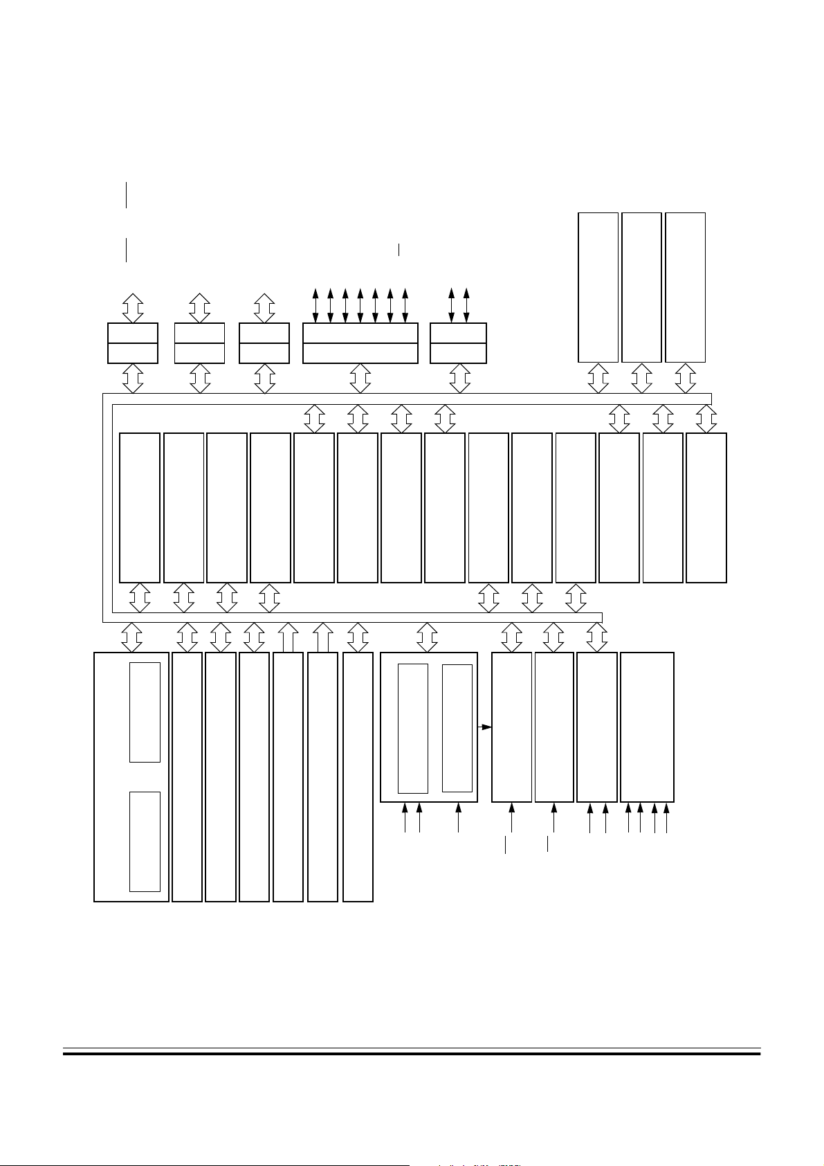
Figure 1-1 shows the struc ture of the MC68HC908GR8.
Technical Data MC68HC908GR8 — Rev 4.0
28 General Description MOTOROLA
For More Information On This Product,
Go to: www.freescale.com
Freescale Semiconductor, Inc.
General Description
MCU Block Diagram
nc...
I
cale Semiconductor,
Frees
–PTA0/KBD0 †
PTD6/T2CH0 †
PTD5/T1CH1 †
PTD4/T1CH0 †
PTA3/KBD3
PORTA
DDRA
INTERNAL BUS
MODULE
PROGR. TIMEBASE
UNIT (ALU)
ARITHMETIC/LOGIC
M68HC08 CPU
PTB5/AD5–PTB0/AD0
PORTB
DDRB
MODULE
SINGLE BRKPT BREAK
DUAL V. LOW-VOLTAGE INH IBI T
PTC1–PTC0 † ‡
PORTC
DDRC
MODULE
4-BIT KEYBOARD
INTERRUPT MODULE
2-CHANNEL TIMER INTERFACE
PTD3/SPSCK †
MODULE 1
MODULE 2
1-CHANNEL TIMER INTERFACE
†
PTE1/RxD
COMPUTER OPERATING
PROPERLY MODULE
PHASE-LOCKED LOOP
PTE0/TxD
PORTE
DDRE
MODULE
POWER-ON RESET
MODULE
DATA BUS SWITCH
INTERFACE MODULE
24 INTR SYSTEM INTEGRATION
MONITOR MODULE
MODULE
MODULE
SINGLE EXTERNAL IRQ
CONVERTER MODULE
8-BIT ANALOG-TO-DIG ITA L
SERIAL PERIPHERAL
MODULE
SECURITY
MODULE
MEMORY MAP
POWER
MODULE
MONITOR MODE ENTRY
MODULE
MASK OPTION REGISTER1
MODULE
MASK OPTION REGISTER2
PTD2/MOSI †
PTD1/MISO †
PTD0/SS
PORTD
DDRD
INTERFACE MODULE
SERIAL COMMUNICATIONS
32-kHz OSCILLATOR
CLOCK GENERATOR MODULE
USER RAM — 384 BYTES
CPU
REGISTERS
MC68HC908GR4 US ER FLA SH — 4096BYTES
MC68HC908GR8 USER FLASH — 7680 BYTES
CONTROL AND STATUS REGISTERS — 64 BYTES
MONITOR ROM — 310 BYTES
OSC1
USER FLASH VECTOR SPACE — 36 BYTES
FLASH PROGRAMMING (BURN-IN) ROM — 544 BYTES
OSC2
CGMXFC
* RST
* IRQ
DD
DDA
SSA
VSSV
REFL
REFH
V
/ V
SSAD
DDAD /
V
V
V
V
† Ports are software configurable with pullup device if input port.
‡ Higher current drive port pins
* Pin contains integrated pullup device
Figure 1-1. MCU Block Diagram
MC68HC908GR8 — Rev 4.0 Technical Data
MOTOROLA General Description 29
For More Information On This Product,
Go to: www.freescale.com
General Description
1.5 Pin Assignments
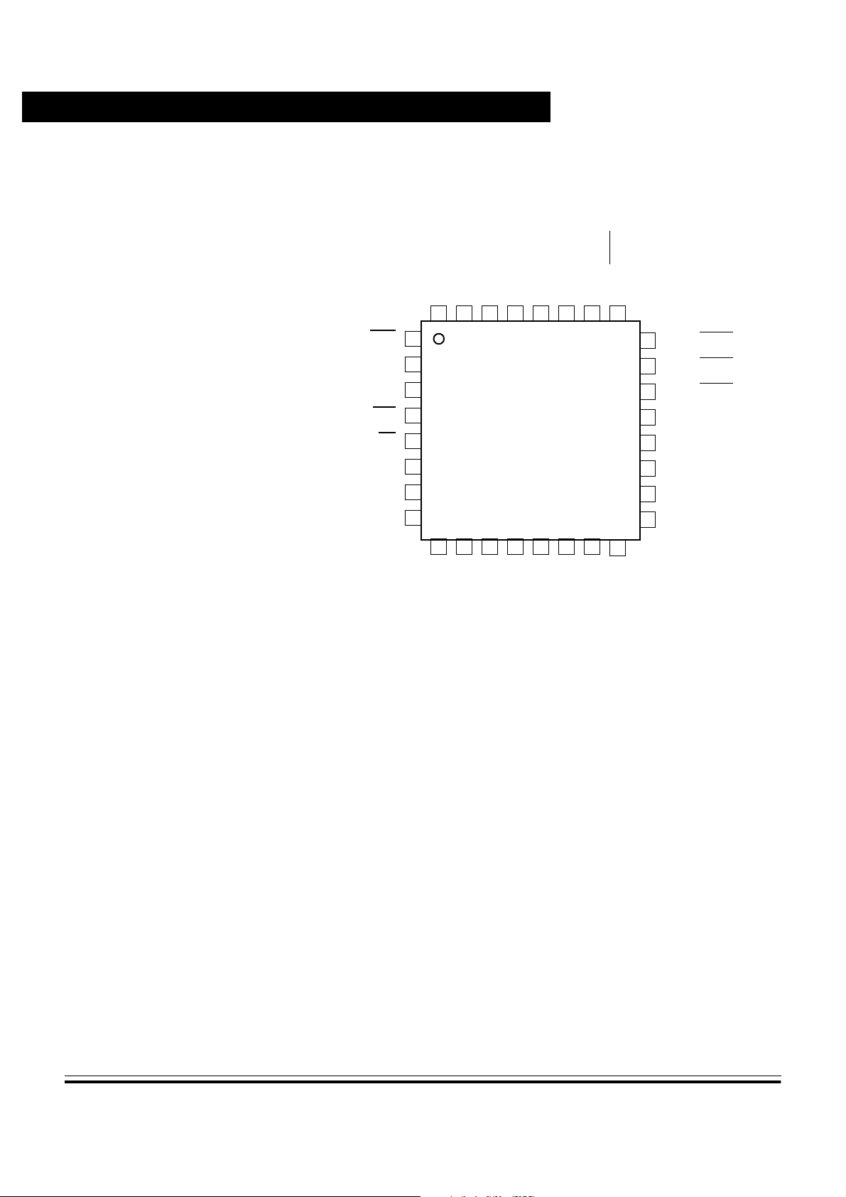
Freescale Semiconductor, Inc.
OSC1
OSC2
32
RST
1
PTE0/TxD
PTE1/RxD
IRQ
nc...
I
PTD0/SS
PTD1/MISO
PTD2/MOSI
PTD3/SPSCK
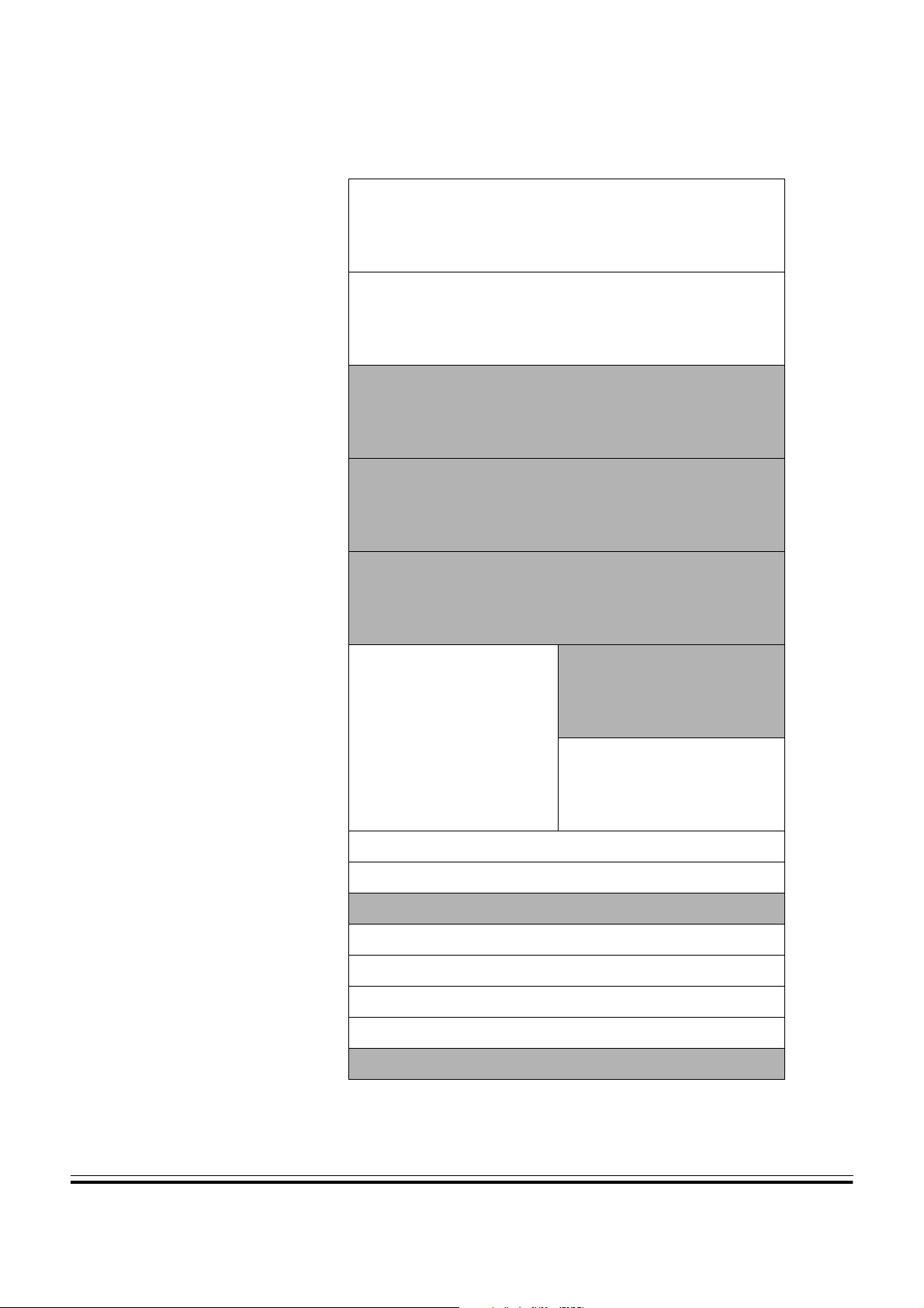
NOTE: Ports PTB4, PTB5, PTC0, and PTC1 are available only with the QFP.
31
2
3
4
5
6
7
8
9
10
SS
DD
V
V
SSAVDDA
CGMXFC
V
29
30
11
12
PTD4/T1CH0
PTD5/T1CH1
28
13
PTD6/T2CH0
PTC1
27
14
PTB0/AD0
Figure 1-2. QFP Pin Assignments
cale Semiconductor,
PTC0
PTB1/AD1
26
15
PTA3/KBD3
25
24
23
22
21
20
19
18
17
16
PTB2/AD2
PTA2/KBD2
PTA1/KBD1
PTA0/KBD0
V
SSAD/VREFL
V
DDAD/VREFH
PTB5/AD5
PTB4/AD4
PTB3/AD3
Frees
Technical Data MC68HC908GR8 — Rev 4.0
30 General Description MOTOROLA
For More Information On This Product,
Go to: www.freescale.com

Freescale Semiconductor, Inc.
General Description
Pin Functions
nc...
I
NOTE: Ports PTB4, PTB5, PTC0, and PTC1 are available only with the QFP.
1.6 Pin Functions
Descriptions of the pin fun cti on s are pr ovide d her e .
1.6.1 Power Supply Pins (VDD and VSS)
VDD and VSS are the power supply and grou nd pins. The MCU opera tes
cale Semiconductor,
Frees
from a single power supply.
Fast signal transitions on MCU pins place high, short-duration current
demands on the power supply. To prevent noise problems, take special
care to provide power supply bypassing at the MCU as Figure 1-4
shows. Place the C1 bypass cap acitor as close to t he MCU as possib le.
Use a high-frequency-response ceramic capacitor for C1. C2 is an
optional bulk current bypass capacitor for use in applications that require
the port pins to source high current levels.
CGMXFC
OSC2
OSC1
RST
PTE0/TxD
PTE1/RxD
IRQ
PTD0/SS
PTD1/MISO
PTD2/MOSI
PTD3/SPSCK
V
V
PTD4/T1CH0
SS
DD
1
2
3
4
5
6
7
8
9
10
11
12
13
14
28
27
26
25
24
23
22
21
20
19
18
17
16
15
V
SSA
V
DDA
PTA3/KBD3
PTA2/KBD2
PTA1/KBD1
PTA0/KBD0
V
SSAD/VREFL
V
DDAD/VREFH
PTB3/AD3
PTB2/AD2
PTB1/AD1
PTB0/AD0
PTD6/T2CH0
PTD5/T1CH1
Figure 1-3. DIP And SOIC Pin Assignments
MC68HC908GR8 — Rev 4.0 Technical Data
MOTOROLA General Description 31
For More Information On This Product,
Go to: www.freescale.com

General Description
Freescale Semiconductor, Inc.
MCU
nc...
I
1.6.2 Oscillator Pins (OSC1 and OSC2)
The OSC1 and OSC2 pins a re the connectio ns for the on-chi p oscillator
circuit. See Clock Generator Module (CGMC).
1.6.3 External Reset Pin (RST)
A logic 0 on the RST pin forces the MCU to a known startup state. RST
is bidirectional, allowing a reset of the entire system. It is driven low when
any internal reset sour ce is asserted. This pin contains an int ernal pullup
resistor that is always activated, even when the reset pin is pulled low.
cale Semiconductor,
1.6.4 External Interrupt Pin (IRQ)
See Resets and Interrupts.
V
DD
C1
µF
0.1
+
C2
V
DD
NOTE: Component values shown represent typical applications.
V
SS
Figure 1-4. Power Supply Bypassing
Frees
IRQ is an asynchronous external interrupt pin. This pin contains an
internal pullup resistor tha t is always activated , even when the re set pin
is pulled low. See External Interrupt (IRQ).
1.6.5 CGM Power Supply Pins (V
V
and V
DDA
and V
DDA
are the power supply pins for the analog portion of the
SSA
SSA
)
clock generator module (CGM). Decoupling of these pins should be as
per the digital supply. See Clock Generator Module (CGMC).
Technical Data MC68HC908GR8 — Rev 4.0
32 General Description MOTOROLA
For More Information On This Product,
Go to: www.freescale.com

Freescale Semiconductor, Inc.
1.6.6 External Filter Capacitor Pin (CGMXFC)
CGMXFC is an external filter capacitor connection for the CGM. See
Clock Generator Module (CGMC).
General Description
Pin Functions
1.6.7 Analog Power Supply/Reference Pins (V
V
DDAD
and V
are the power supply pins for the analog-to-digital
SSAD
DDAD/VREFH
converter. Decoupli n g o f these pins should be as per the digital supp l y.
NOTE: V
internally connected with V
nc...
I
V
V
internally connected wi th V
V
is the high reference supply for the ADC. The V
REFH
DDAD
should be tied to the same potential as VDD via separate traces.
DDAD
is the low reference supply for the ADC. The V
REFL
SSAD
should be tied to the same potential as VSS via separate traces.
SSAD
See Analog-to-Digital Converter (ADC).
1.6.8 Port A Input/Output (I/O) Pins (PTA3/KBD3–PTA0/KBD0)
PTA3–PTA0 are special-function, bidirectional I/O port pins. Any or all of
the port A pins can be progr ammed to ser ve as keybo ard interr upt pins.
See Input/Output Ports (I/O) and External Interrupt (IRQ).
These port pins also have selectable pullups when configured for input
cale Semiconductor,
mode. The pullups are disengaged when configured for output mode.
The pullups are selectable on an individual port bit basis.
When the port pins are configured for special-function mode (KBI),
Frees
pullups will be automatically engaged. As long as the port pins are in
special-function mode, the pullups will always be on.
and V
SSAD/VREFL
)
REFH
signal is
and have the same pote ntial a s V
pin is
REFL
and has the same potential as V
DDAD.
SSAD.
1.6.9 Port B I/O Pins (PTB5/AD5–PTB0/AD0)
PTB5–PTB0 are special-function, bi directional I/O port p ins that can also
be used for anal og-to-digital converter (ADC) inp uts. See Input/Output
Ports (I/O) and Analog-to-Digital Converter (ADC).
There are no pullups associated with this port.
MC68HC908GR8 — Rev 4.0 Technical Data
MOTOROLA General Description 33
For More Information On This Product,
Go to: www.freescale.com

Freescale Semiconductor, Inc.
General Description
1.6.10 Port C I/O Pins (PTC1–PTC0)
PTC1–PTC0 are general-purpose, bidirectional I/O port pins. See
Input/Output Ports (I/O). PTC0 and PTC1 are only available on 32-pin
QFP packages.
These port pins also have selectable pullups when configured for input
mode. The pullups are disengaged when configured for output mode.
The pullups are selectable on an individual port bit basis.
1.6.11 Port D I/O Pins (PTD6/T2CH0–PTD0/SS)
nc...
I
1.6.12 Port E I/O Pins (PTE1/RxD–PTE0/TxD)
PTD6–PTD0 are special-function, bidirectional I/O port pins.
PTD3–PTD0 can be programm ed t o b e seri al p eriph eral i nter fac e (SP I)
pins, while PTD6–PTD4 can be individually programmed to be timer
interface module (TIM1 and TIM2) pins. See Timer Interface Module
(TIM), Serial Peripheral Interface (SPI), and Input/Output Ports (I/O).
These port pins also have selectable pullups when configured for input
mode. The pullups are disengaged when configured for output mode.
The pullups are selectable on an individual port bit basis.
When the port pins are configured for special-function mode (SPI, TIM1,
TIM2), pullups can be selectable on an individual port pin basis.
cale Semiconductor,
PTE1–PTE0 are special-function, bidir ectional I/O po rt pins. These pi ns
can also be programmed to be serial communications interface (SCI)
Frees
pins. See Serial Communications Inte rface (SCI) and Input/Output Ports
(I/O).
NOTE: Any unused inputs and I/O ports should be tied to an appropriate logic
level (either VDD or VSS). Although the I/O ports of the MC68H C908GR8
do not require termination, termination is recommended to reduce the
possibility of electro-static discharge damage.
Technical Data MC68HC908GR8 — Rev 4.0
34 General Description MOTOROLA
For More Information On This Product,
Go to: www.freescale.com

Freescale Semiconductor, Inc.
Technical Data — MC68HC908GR8
2.1 Contents
2.2 Introduction. . . . . . . . . . . . . . . . . . . . . . . . . . . . . . . . . . . . . . . .35
2.3 Unimplemented Memory Locations . . . . . . . . . . . . . . . . . . . . . .35
Section 2. Memory Map
nc...
I
2.2 Introduction
cale Semiconductor,
Frees
2.4 Reserved Memory Locations . . . . . . . . . . . . . . . . . . . . . . . . . .36
2.5 Input/Output (I/O) Section. . . . . . . . . . . . . . . . . . . . . . . . . . . . .36
The CPU08 can address 64K bytes of memory space. The memory
map, shown in Figure 2-1, includes:
• 8K bytes of FLA SH memory, 7680 bytes of user space on the
MC68HC908GR8 or
4K bytes of FLA SH memory, 4096 bytes of user space on the
MC68HC908GR4
• 384 bytes of random-access memory (RAM)
• 36 bytes of user-defined vectors
• 310 bytes of monitor routines in read-only memory (ROM)
• 544 bytes of integrated FLAS H bu rn -i n rout ines in ROM
2.3 Unimplemented Memory Locations
Accessing an unimplemented location can cause an illegal address
reset if illegal address resets are enabled. In the memory map (Figure 2-
1) and in register figures in this document, unimplemented locations are
shaded.
MC68HC908GR8 — Rev 4.0 Technical Data
MOTOROLA Memory Map 35
For More Information On This Product,
Go to: www.freescale.com

Freescale Semiconductor, Inc.
Memory Map
2.4 Reserved Memory Locations
Accessing a reserved location can have unpredictable effects on MCU
operation. In t he Figure 2-1 and in register figures in this document,
reserved locations ar e marke d with the w ord Reser ved or wi th the le tter
R.
2.5 Input/Output (I/O) Section
Most of the control, status, and data registers are in the zero page area
of $0000–$003F. Additional I/O registers have these addresses:
nc...
I
cale Semiconductor,
Frees
• $FE00; SIM break status register, SBSR
• $FE01; SIM reset status register, SRSR
• $FE03; SIM break flag control register, SBFCR
• $FE09; interrupt status register 1, INT1
• $FE0A; interrupt status register 2, INT2
• $FE0B; interrupt status register 3, INT3
• $FE07; reserved FLASH test cont rol register, FLTCR
• $FE08; FLASH control register, FLCR
• $FE09; break address register high, BRKH
• $FE0A; break ad dress register low, BRKL
• $FE0B; break status and control register, BRKSCR
• $FE0C; LVI status register, LVISR
• $FF7E; FLASH block protect reg ister , FL BPR
Data registers are shown in Figure 2-2, and Table 2-1 is a list of vector
locations.
Technical Data MC68HC908GR8 — Rev 4.0
36 Memory Map MOTOROLA
For More Information On This Product,
Go to: www.freescale.com
Freescale Semiconductor, Inc.
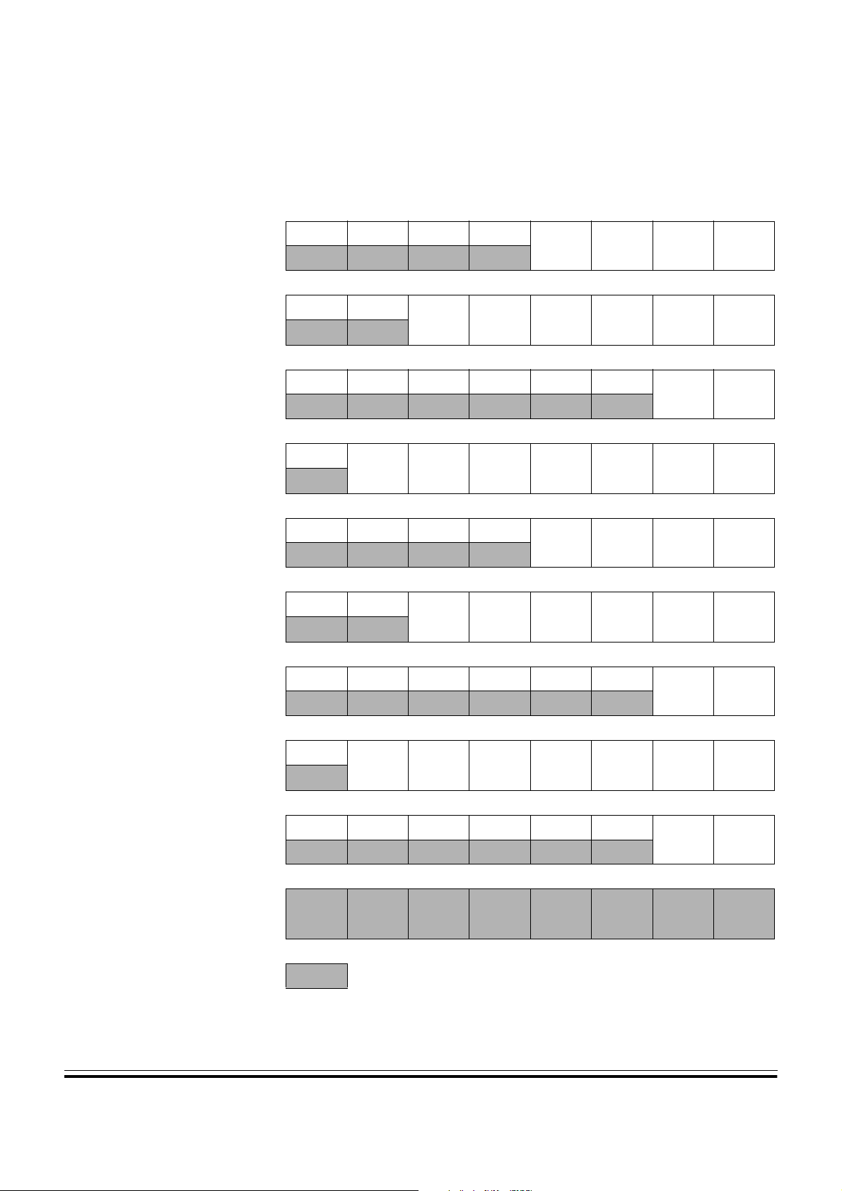
$0000
↓
$003F
$0040
↓
$01BF
$01C0
↓
$1BFF
I/O Registers
64 Bytes
RAM
384 Bytes
Unimplemented
6720 Bytes
Memory Map
Input/Output (I/O) Section
nc...
I
cale Semiconductor,
Frees
$1C00
↓
$1E1F
$1E20
↓
$DFFF
$E000
↓
$EDFF
$EE00
↓
$FDFF
$FE00 SIM Break Status Register (SBSR)
$FE01 SIM Reset Status Register (SRSR)
$FE02
Reserved for Integrated FLASH Burn-in Routines
544 Bytes
Unimplemented
49,632 Bytes
MC68HC908GR4
Unimplemented
MC68HC908GR8
FLASH Memory
7680 Bytes
Reserved
3584 Bytes
MC68HC908GR4
FLASH Memory
4096 Bytes
$FE03 SIM Break Flag Control Register (SBFCR)
$FE09 Interrupt Status Register 1 (INT1)
$FE0A Interrupt Status Register 2 (INT2)
$FE0B Interrupt Status Register 3 (INT3)
$FE07
Reserved for FLASH Test Control Register (FLTCR)
Figure 2-1. Memory Map
MC68HC908GR8 — Rev 4.0 Technical Data
MOTOROLA Memory Map 37
For More Information On This Product,
Go to: www.freescale.com

Memory Map
Freescale Semiconductor, Inc.
$FE08 FLASH Control Register (FLCR)
$FE09 Break Address Register High (BRKH)
$FE0A Break Address Register Low (BRKL)
$FE0B Break Status and Control Register (BRKSCR)
$FE0C LVI Status Register (LVISR)
$FE0D
↓
$FE0F
Reserved
3 Bytes
nc...
I
cale Semiconductor,
Frees
$FE10
↓
$FE1F
$FE20
↓
$FF55
Note: $FFF6–$FFFD
contains
8 security bytes
$FF56
↓
$FF7D
$FF7E FLASH Block Protect Register (FLBPR)
$FF7F
↓
$FFDB
$FFDC
↓
$FFFE
Reserved for Compatibility with Monitor Code
Unimplemented
16 Bytes
for A-Family Parts
Monitor ROM
310 Bytes
Unimplemented
40 Bytes
Unimplemented
93 Bytes
FLASH Vectors
(36 Bytes inluding $FFFF)
$FFFF
Low byte of reset vector when read
COP Control Register (COPCTL)
Figure 2-1. Memory Map (Continued)
Technical Data MC68HC908GR8 — Rev 4.0
38 Memory Map MOTOROLA
For More Information On This Product,
Go to: www.freescale.com
Freescale Semiconductor, Inc.
Memory Map
Input/Output (I/O) Section
Addr.Register Name Bit 7654321Bit 0
nc...
I
cale Semiconductor,
Frees
$0000
$0001
$0002
$0003
$0004
$0005
$0006
$0007
$0008
Port A Data Register
Port B Data Register
Port C Data Register
Port D Data Register
Data Direction Register A
Data Direction Register B
Data Direction Register C
Data Direction Register D
Port E Data Register
(PTA)
(PTB)
(PTC)
(PTD)
(DDRA)
(DDRB)
(DDRC)
(DDRD)
(PTE)
Read: 0000
PTA3 PTA2 PTA1 PTA0
Write:
Reset: Unaffected by reset
Read: 0 0
PTB5 PTB4 PTB3 PTB2 PTB1 PTB0
Write:
Reset: Unaffected by reset
Read: 000000
PTC1 PTC0
Write:
Reset: Unaffected by reset
Read: 0
PTD6 PTD5 PTD4 PTD3 PTD2 PTD1 PTD0
Write:
Reset: Unaffected by reset
Read: 0000
DDRA3 DDRA2 DDRA1 DDRA0
Write:
Reset:00000000
Read: 0 0
DDRB5 DDRB4 DDRB3 DDRB2 DDRB1 DDRB0
Write:
Reset:00000000
Read: 000000
DDRC1 DDRC0
Write:
Reset:00000000
Read: 0
DDRD6 DDRD5 DDRD4 DDRD3 DDRD2 DDRD1 DDRD0
Write:
Reset:00000000
Read: 000000
PTE1 PTE0
Write:
Reset: Unaffected by reset
Read:
$0009 Unimplemented
Write:
Reset:00000000
= Unimplemented R = Reserved U = Unaffected
Figure 2-2. Control, Status, and Data Registers (Sheet 1 of 8)
MC68HC908GR8 — Rev 4.0 Technical Data
MOTOROLA Memory Map 39
For More Information On This Product,
Go to: www.freescale.com
Freescale Semiconductor, Inc.
Memory Map
Addr.Register Name Bit 7654321Bit 0
Read:
nc...
I
cale Semiconductor,
Frees
$000A Unimplemented
$000B Unimplemented
$000C
$000D
$000E
$000F
$0010
$0011
$0012
Data Direction Register E
Port A Input Pullup Enable
Register (PTAPUE)
Port C Input Pullup Enable
Register (PTCPUE)
Port D Input Pullup Enable
Register (PTDPUE)
SPI Control Register
SPI Status and Control
Register (SPSCR)
SPI Data Register
(DDRE)
(SPCR)
(SPDR)
Write:
Reset:00000000
Read:
Write:
Reset:00000000
Read: 000000
Write:
Reset:00000000
Read: 0000
Write:
Reset:00000000
Read: 000000
Write:
Reset:00000000
Read: 0
Write:
Reset:00000000
Read:
SPRIE
Write:
Reset:00101000
Read: SPRF
Write:
Reset:00001000
Read: R7 R6 R5 R4 R3 R2 R1 R0
Write: T7 T6 T5 T4 T3 T2 T1 T0
Reset: Unaffected by reset
PTDPUE6 PTDPUE5 PTDPUE4 PTDPUE3 PTDPUE2 PTDPUE1 PTDPUE0
DMAS
SPMSTR CPOL CPHA SPWOM SPE SPTIE
OVRF MODF SPTE
ERRIE
PTAPUE3 PTAPUE2 PTAPUE1 PTAPUE0
MODFEN SPR1 SPR0
DDRE1 DDRE0
PTCPUE1 PTCPUE0
$0013
SCI Control Register 1
(SCC1)
Read:
Write:
Reset:00000000
LOOPS ENSCI TXINV M WAKE ILTY PEN PTY
= Unimplemented R = Reserved U = Unaffected
Figure 2-2. Control, Status, and Data Registers (Sheet 2 of 8)
Technical Data MC68HC908GR8 — Rev 4.0
40 Memory Map MOTOROLA
For More Information On This Product,
Go to: www.freescale.com
Freescale Semiconductor, Inc.
Addr.Register Name Bit 7654321Bit 0
Memory Map
Input/Output (I/O) Section
nc...
I
cale Semiconductor,
Frees
$0014
$0015
$0016
$0017
$0018
$0019
$001A
$001B
$001C
SCI Control Register 2
SCI Control Register 3
SCI Status Register 1
SCI Status Register 2
SCI Baud Rate Register
and Control Register
Keyboard Interrupt Enable
Register (INTKBIER)
Time Base Module Control
(SCC2)
(SCC3)
(SCS1)
(SCS2)
SCI Data Register
(SCDR)
(SCBR)
Keyboard Status
(INTKBSCR)
Register (TBCR)
Read:
Write:
Reset:00000000
Read: R8
Write:
Reset:UU000000
Read: SCTE TC SCRF IDLE OR NF FE P E
Write:
Reset:11000000
Read:
Write:
Reset:00000000
Read: R7 R6 R5 R4 R3 R2 R1 R0
Write: T7 T6 T5 T4 T3 T2 T1 T0
Reset: Unaffected by reset
Read:
Write:
Reset:00000000
Read: 0000KEYF0
Write:
Reset:00000000
Read:
Write:
Reset: 0000
Read: TBIF
Write:
Reset:00000000
SCTIE TCIE SCRIE ILIE TE RE RWU SBK
T8 DMARE DMATE ORIE NEIE FEIE PEIE
BKF RPF
SCP1 SCP0 R SCR2 SCR1 SCR0
IMASKK MODEK
TBR2 TBR1 TBR0
ACKK
KBIE3 KBIE2 KBIE1 KBIE0
0
TBIE TBON R
TACK
$001D
IRQ Status and Control
Register (INTSCR)
Read: 0000IRQF10
Write:
Reset:00000000
= Unimplemented R = Reserved U = Unaffected
ACK1
IMASK1 MODE1
Figure 2-2. Control, Status, and Data Registers (Sheet 3 of 8)
MC68HC908GR8 — Rev 4.0 Technical Data
MOTOROLA Memory Map 41
For More Information On This Product,
Go to: www.freescale.com

Freescale Semiconductor, Inc.
Memory Map
Addr.Register Name Bit 7654321Bit 0
nc...
I
cale Semiconductor,
Frees
Configuration Register 2
$001E
$001F
$0020
$0021
$0022
$0023
$0024
$0025
$0026
Configuration Register 1
Timer 1 Status and Control
Timer 1 Counter Register
Timer 1 Counter Register
Timer 1 Counter Modulo
Register High (T1MODH)
Timer 1 Counter Modulo
Register Low (T1MODL)
Timer 1 Channel 0 Status
Register High (T1CH0H)
(CONFIG2)†
(CONFIG1)
Register (T1SC)
High (T1CNTH)
Low (T1CNTL)
and Control Register
(T1SC0)
Timer 1 Channel 0
Read: 000000
Write:
Reset:00000000
Read:
Write:
†
Reset:00000000
Read: TOF
Write: 0 TRST
Reset:00100000
Read: Bit 15 14 13 12 11 10 9 Bit 8
Write:
Reset:00000000
Read: Bit 7 654321Bit 0
Write:
Reset:00000000
Read:
Write:
Reset:11111111
Read:
Write:
Reset:11111111
Read: CH0F
Write: 0
Reset:00000000
Read:
Write:
Reset: Indeterminate after reset
COPRS LVISTOP LVIRSTD LVIPWRD LVI5OR3
00
TOIE TSTOP
Bit 15 14 13 12 11 10 9 Bit 8
Bit 7654321Bit 0
CH0IE MS0B MS0A ELS0B ELS0A TOV0 CH0MAX
Bit 15 14 13 12 11 10 9 Bit 8
†
SSREC STOP COPD
PS2 PS1 PS0
OSC-
STOPENB
SCIBD-
SRC
Read:
$0027
† One-time writeable register after each reset, except LVI5OR3 bit. LVI5OR3 bit is only reset via POR (power-on reset).
Timer 1 Channel 0
Register Low (T1CH0L)
Write:
Reset: Indeterminate after reset
Bit 7654321Bit 0
= Unimplemented R = Reserved U = Unaffected
Figure 2-2. Control, Status, and Data Registers (Sheet 4 of 8)
Technical Data MC68HC908GR8 — Rev 4.0
42 Memory Map MOTOROLA
For More Information On This Product,
Go to: www.freescale.com

Freescale Semiconductor, Inc.
Addr.Register Name Bit 7654321Bit 0
Memory Map
Input/Output (I/O) Section
nc...
I
cale Semiconductor,
Frees
Timer 1 Channel 1 Status
$0028
$0029
$002A
$002B
$002C
$002D
$002E
$002F
$0030
and Control Register
Timer 1 Channel 1
Register High (T1CH1H)
Timer 1 Channel 1
Register Low (T1CH1L)
Timer 2 Status and Control
Timer 2 Counter Register
Timer 2 Counter Register
Timer 2 Counter Modulo
Register High (T2MODH)
Timer 2 Counter Modulo
Register Low (T2MODL)
Timer 2 Channel 0 Status
and Control Register
(T1SC1)
Register (T2SC)
High (T2CNTH)
Low (T2CNTL)
(T2SC0)
Read: CH1F
CH1IE
Write: 0
Reset:00000000
Read:
Bit 15 14 13 12 11 10 9 Bit 8
Write:
Reset: Indeterminate after reset
Read:
Bit 7654321Bit 0
Write:
Reset: Indeterminate after reset
Read: TOF
TOIE TSTOP
Write: 0 TRST
Reset:00100000
Read: Bit 15 14 13 12 11 10 9 Bit 8
Write:
Reset:00000000
Read: Bit 7 654321Bit 0
Write:
Reset:00000000
Read:
Bit 15 14 13 12 11 10 9 Bit 8
Write:
Reset:11111111
Read:
Bit 7654321Bit 0
Write:
Reset:11111111
Read: CH0F
CH0IE MS0B MS0A ELS0B ELS0A TOV0 CH0MAX
Write: 0
Reset:00000000
0
MS1A ELS1B ELS1A TOV1 CH1MAX
00
PS2 PS1 PS0
$0031
Timer 2 Channel 0
Register High (T2CH0H)
Read:
Write:
Reset: Indeterminate after reset
Bit 15 14 13 12 11 10 9 Bit 8
= Unimplemented R = Reserved U = Unaffected
Figure 2-2. Control, Status, and Data Registers (Sheet 5 of 8)
MC68HC908GR8 — Rev 4.0 Technical Data
MOTOROLA Memory Map 43
For More Information On This Product,
Go to: www.freescale.com

Freescale Semiconductor, Inc.
Memory Map
Addr.Register Name Bit 7654321Bit 0
nc...
I
cale Semiconductor,
Frees
$0032
$0033
$0034 Unimplemented
$0035 Unimplemented
$0036
$0037
$0038
$0039
$003A
Timer 2 Channel 0
Register Low (T2CH0L)
Unimplemented
PLL Control Register
PLL Bandwidth Control
Register (PBWC)
PLL Multiplier Select High
Register (PMSH)
PLL Multiplier Select Low
Register (PMSL)
PLL VCO Select Range
Register (PMRS)
(PCTL)
Read:
Write:
Reset: Indeterminate after reset
Read:
Write:
Reset:00000000
Read:
Write:
Reset: Indeterminate after reset
Read:
Write:
Reset: Indeterminate after reset
Read:
Write:
Reset:00100000
Read:
Write:
Reset:00000000
Read: 0000
Write:
Reset:00000000
Read:
Write:
Reset:01000000
Read:
Write:
Reset:01000000
Bit 7654321Bit 0
PLLIE
AUTO
MUL7 MUL6 MUL5 MUL4 MUL3 MUL2 MUL1 MUL0
VRS7 VRS6 VRS5 VRS4 VRS3 VRS2 VRS1 VRS0
PLLF
LOCK
PLLON BCS PRE1 PRE0 VPR1 VPR0
ACQ
0000
R
MUL11 MUL10 MUL9 MUL8
$003B
PLL Reference Divider
Select Register (PMDS)
Read: 0000
Write:
Reset:00000001
= Unimplemented R = Reserved U = Unaffected
RDS3 RDS2 RDS1 RDS0
Figure 2-2. Control, Status, and Data Registers (Sheet 6 of 8)
Technical Data MC68HC908GR8 — Rev 4.0
44 Memory Map MOTOROLA
For More Information On This Product,
Go to: www.freescale.com

Freescale Semiconductor, Inc.
Addr.Register Name Bit 7654321Bit 0
Memory Map
Input/Output (I/O) Section
nc...
I
cale Semiconductor,
Frees
Analog-to-Digital Status
$003C
$003D
$003E
$003F Unimplemented
$FE00
$FE01
$FE02 Unimplemented
$FE03
$FE09
and Control Register
(ADSCR)
Analog-to-Digital Data
Register (ADR)
Analog-to-Digital Input
Clock Register (ADCLK)
SIM Break Status Register
(SBSR)
Note: Writing a logic 0 clears SBSW.
SIM Reset Status Register
(SRSR)
SIM Break Flag Control
Register (SBFCR)
Interrupt Status Register 1
(INT1)
Read: COCO
Write: R
Reset:00011111
Read: AD7 AD6 AD5 AD4 AD3 AD2 AD1 AD0
Write:RRRRRRRR
Reset: Indeterminate after reset
Read:
ADIV2 ADIV1 ADIV0 ADICLK
Write: RRRR
Reset:00000000
Read:
Write:
Reset:
Read:
RRRRRR
Write: NOTE
Reset:00000000
Read: POR PIN COP ILOP ILAD MODRST LVI 0
Write:
POR:10000000
Read:
Write:
Reset:
Read:
BCFERRRRRRR
Write:
Reset: 0
Read: IF6 IF5 IF4 IF3 IF2 IF1 0 0
Write:RRRRRRRR
Reset:00000000
AIEN ADCO ADCH4 ADCH3 ADCH2 ADCH1 ADCH0
0000
SBSW
R
Read: IF14 IF13 IF12 IF11 IF10 IF9 IF8 IF7
Interrupt Status Register 2
$FE0A
Write:RRRRRRRR
(INT2)
Reset:00000000
= Unimplemented R = Reserved U = Unaffected
Figure 2-2. Control, Status, and Data Registers (Sheet 7 of 8)
MC68HC908GR8 — Rev 4.0 Technical Data
MOTOROLA Memory Map 45
For More Information On This Product,
Go to: www.freescale.com

Freescale Semiconductor, Inc.
Memory Map
Addr.Register Name Bit 7654321Bit 0
Read: 000000IF16IF15
Interrupt Status Register 3
$FE0B
Write:RRRRRRRR
(INT3)
Reset:00000000
nc...
I
cale Semiconductor,
Frees
Read:
$FE07
$FE08
$FE09
$FE0A
$FE0B
$FE0C
$FF7E
$FFFF
FLASH Test Control
Register (FLTCR)
FLASH Control Register
(FLCR)
Break Address Register
High (BRKH)
Break Address Register
Low (BRKL)
Break Status and Control
Register (BRKSCR)
LVI Status Register
(LVISR)
FLASH Block Protect
Register (FLBPR)
COP Control Register
(COPCTL)
Write:
Reset:00000000
Read: 0000
Write:
Reset:00000000
Read:
Write:
Reset:00000000
Read:
Write:
Reset:00000000
Read:
Write:
Reset:00000000
Read: LVIOUT 0000000
Write:
Reset:00000000
Read:
Write:
†
Reset:UUUUUUUU
Read: Low byte of reset vector
Write: Writing clears COP counter (any value)
Reset: Unaffected by reset
RRRRRRRR
HVEN MASS ERASE PGM
Bit 15 14 13 12 11 10 9 Bit 8
Bit 7654321Bit 0
000000
BRKE BRKA
BPR7 BPR6 BPR5 BPR4 BPR3 BPR2 BPR1 BPR0
† Non-volatile FLASH register
= Unimplemented R = Reserved U = Unaffected
Figure 2-2. Control, Status, and Data Registers (Sheet 8 of 8)
Technical Data MC68HC908GR8 — Rev 4.0
46 Memory Map MOTOROLA
For More Information On This Product,
Go to: www.freescale.com

Freescale Semiconductor, Inc.
Memory Map
Input/Output (I/O) Section
nc...
I
cale Semiconductor,
Frees
Table 2-1. Vector Addresses
.
Vector Priority Vector Address Vector
Lowest
IF16
IF15
IF14
IF13
IF12
IF11
IF10
IF9
IF8
IF7
IF6
IF5
IF4
IF3
IF2
IF1
—
—
Highest $FFFF Reset Vector (Low)
$FFDC Timebase Vector (High)
$FFDD Timebase Vector (Low)
$FFDE ADC Conversion Complete Vector (High)
$FFDF ADC Conversion Complete Vector (Low)
$FFE0 Keyboard Vector (High)
$FFE1 Keyboard Vector (Low)
$FFE2 SCI Transmit Vector (High)
$FFE3 SCI Transmit Vector (Low)
$FFE4 SCI Receiv e Vector (High)
$FFE5 SCI Receiv e Vector (Low)
$FFE6 SCI Error Vector (High)
$FFE7 SCI Error Vector (Low)
$FFE8 SPI Transmit Vector (High)
$FFE9 SPI Transmit Vector (Low)
$FFEA SPI Receive Vector (High)
$FFEB SPI Receive Vector (Low)
$FFEC TIM2 Overflow Vector (High)
$FFED TIM2 Overflow Vector (Low)
$FFEE
$FFEF
$FFF0 TIM2 Channel 0 Vector (High)
$FFF1 TIM2 Channel 0 Vector (Low)
$FFF2 TIM1 Overflow Vector (High)
$FFF3 TIM1 Overflow Vector (Low)
$FFF4 TIM1 Channel 1 Vector (High)
$FFF5 TIM1 Channel 1 Vector (Low)
$FFF6 TIM1 Channel 0 Vector (High)
$FFF7 TIM1 Channel 0 Vector (Low)
$FFF8 PLL Vector (High)
$FFF9 PLL Vector (Low)
$FFFA IRQ
$FFFB IRQ
$FFFC SWI Vector (High)
$FFFD SWI Vector (Low)
$FFFE Reset Vector (High)
Reserved
Reserved
Vector (High)
Vector (Low)
MC68HC908GR8 — Rev 4.0 Technical Data
MOTOROLA Memory Map 47
For More Information On This Product,
Go to: www.freescale.com

Memory Map
nc...
I
Freescale Semiconductor, Inc.
cale Semiconductor,
Frees
Technical Data MC68HC908GR8 — Rev 4.0
48 Memory Map MOTOROLA
For More Information On This Product,
Go to: www.freescale.com

Freescale Semiconductor, Inc.
Technical Data — MC68HC908GR8
3.1 Contents
3.2 Introduction. . . . . . . . . . . . . . . . . . . . . . . . . . . . . . . . . . . . . . . .49
3.3 Analog-to-Digital Converter (ADC). . . . . . . . . . . . . . . . . . . . . .50
Section 3. Low Power Modes
nc...
I
cale Semiconductor,
Frees
3.4 Break Module (BRK). . . . . . . . . . . . . . . . . . . . . . . . . . . . . . . . .51
3.5 Central Processor Unit (CPU). . . . . . . . . . . . . . . . . . . . . . . . . .51
3.6 Clock Generator Module (CGM). . . . . . . . . . . . . . . . . . . . . . . . 52
3.7 Computer Operating Properly Module (COP). . . . . . . . . . . . . .52
3.8 External Interrupt Module (IRQ) . . . . . . . . . . . . . . . . . . . . . . . .53
3.9 Keyboard Interrupt Module (KBI) . . . . . . . . . . . . . . . . . . . . . . .53
3.10 Low-Voltage Inhibit Module (LVI) . . . . . . . . . . . . . . . . . . . . . . .54
3.11 Serial Communications Interface Module (SCI) . . . . . . . . . . . .54
3.12 Serial Peripheral Interface Module (SPI) . . . . . . . . . . . . . . . . .55
3.13 Timer Interface Module (TIM1 and TIM2). . . . . . . . . . . . . . . . .55
3.14 Timebase Module (TBM) . . . . . . . . . . . . . . . . . . . . . . . . . . . . .56
3.15 Exiting Wait Mode. . . . . . . . . . . . . . . . . . . . . . . . . . . . . . . . . . .57
3.16 Exiting Stop Mode. . . . . . . . . . . . . . . . . . . . . . . . . . . . . . . . . . .58
3.2 Introduction
The MCU may enter two low-power modes: wait mode and stop mode.
They are common to a ll HC08 MCUs and are entere d through instruction
execution. This section describes how each module acts in the lowpower modes.
MC68HC908GR8 — Rev 4.0 Technical Data
MOTOROLA Low Power Modes 49
For More Information On This Product,
Go to: www.freescale.com

Low Power Modes
3.2.1 Wait Mode
3.2.2 Stop Mode
nc...
I
Freescale Semiconductor, Inc.
The WAIT instruction puts the MCU in a low-power standby mode in
which the CPU clock is disabled but the bus clock continues to run.
Power consumption can be furt her reduced by disabling the LVI mo dule
and/or the timebase module through bits in the CONFIG register. (See
Configuration Regis ter (CONFIG).)
Stop mode is entered when a STOP instruction is executed. The CPU
clock is disabled and the bus clock is disabled if the OSCSTOPENB bit
in the CONFIG register is at a logic 0. (See Configuration Register
(CONFIG).)
3.3 Analog-to-Digital Converter (ADC)
3.3.1 Wait Mode
The ADC continues normal operation during wait mode. Any enabled
CPU interrupt request from the ADC can bring th e MCU out of wait
mode. If the ADC is not required to bring the MCU out of wait mode,
power down the ADC by setting ADCH4–ADCH0 bits in the ADC status
and control register before executing the WAIT instruction.
cale Semiconductor,
3.3.2 Stop Mode
Frees
The ADC module is inactive after the execution of a S T OP instruction.
Any pending conversion is aborted. ADC conversions resume when the
MCU exits stop mode after an external interrupt. Allow one conversion
cycle to stabilize the analog circuitry.
Technical Data MC68HC908GR8 — Rev 4.0
50 Low Power Modes MOTOROLA
For More Information On This Product,
Go to: www.freescale.com

3.4 Break Module (BRK)
3.4.1 Wait Mode
3.4.2 Stop Mode
nc...
I
Freescale Semiconductor, Inc.
If enabled, the bre ak module is active i n wait mode . In the break routi ne,
the user can subtract one from the return address on the stack if the BW
bit in the break status register is set.
The break module is ina ctive in stop mode. A break in terrupt causes exit
from stop mode and sets the BW bit in the break status register. The
STOP instruction does not affect break module register states.
Low Power Modes
Break Module (BRK)
3.5 Central Processor Unit (CPU)
3.5.1 Wait Mode
The WAIT instruction:
• Clears the interrupt mask (I bit) in the condition code register,
cale Semiconductor,
3.5.2 Stop Mode
• Disables the CPU clock
Frees
The STOP instruction:
• Clears the interrupt mask (I bit) in the condition code register,
enabling interrupts. After exit from wait mod e by interrupt, the I bit
remains clear. After exit by reset, the I bit is set.
enabling external in terrupts. After exit from stop mode by external
interrupt, the I bit remains clear. After exit by reset, the I bit is set.
• Disables the CPU clock
After exiting stop mode, the CPU clock begins running after the oscillator
stabilization delay.
MC68HC908GR8 — Rev 4.0 Technical Data
MOTOROLA Low Power Modes 51
For More Information On This Product,
Go to: www.freescale.com

Freescale Semiconductor, Inc.
Low Power Modes
3.6 Clock Generator Module (CGM)
3.6.1 Wait Mode
The CGM remains active in wait mode. Before entering wait mode,
software can disengage and turn off the PLL by clearing the BCS and
PLLON bits in the PLL control register (PCTL). Less power-sensitive
applications can disengage the PLL without turning it off. Applications
that require the PLL to wake the M CU from wait mode al so can deselect
the PLL output without turning off the PLL.
nc...
I
3.6.2 Stop Mode
If the OSCSTOPEN bit in the CONFIG register is cleared (default), then
the STOP instruction disables the CGM (oscillator and phase-locked
loop) and holds low all CGM outputs (CGMXCLK, CGMOUT, and
CGMINT).
cale Semiconductor,
If the STOP instruction is executed with the VCO clock, CGMVCLK,
divided by two driv ing C GM OU T, th e P LL automatically cle ar s th e BCS
bit in the PLL control register (PCTL), thereby selecting the crystal clock,
CGMXCLK, divided by two as t he source of CGMOUT. When t he MC U
recovers from STOP, the crystal clock divided by two drives CGMOUT
and BCS remains clear.
If the OSCSTOPEN bit in the CONFIG register is set, then the phase
locked loop is shut off, but the oscillator will continue to operate in stop
mode.
Frees
3.7 Computer Operating Properly Module (COP)
3.7.1 Wait Mode
The COP remains active in wait mode. To prevent a COP reset during
wait mode, per iodically clear the COP coun ter in a CPU interrupt rou tine
or a DMA service routine.
Technical Data MC68HC908GR8 — Rev 4.0
52 Low Power Modes MOTOROLA
For More Information On This Product,
Go to: www.freescale.com

Freescale Semiconductor, Inc.
3.7.2 Stop Mode
Stop mode turns off the CGMXCLK input to the COP and clea rs the COP
prescaler. Service the COP immediately be for e en ter i ng or a fte r exi ti ng
stop mode to ensure a full COP timeout period after entering or exiting
stop mode.
The STOP bit in t he configura tion registe r (CONFIG) enables the STOP
instruction. To prevent inadvertently turning off the COP with a STOP
instruction, disable the STOP instruction by clearing the STOP bit.
3.8 External Interrupt Module (IRQ)
nc...
I
Low Power Modes
External Interrupt Module (IRQ)
3.8.1 Wait Mode
The IRQ module remains active in wait mode. Clearing the IMASK1 bit
in the IRQ status and control register enables IRQ CPU interrupt
requests to bring the MCU out of wait mode.
3.8.2 Stop Mode
The IRQ module remains active in stop mode. Clearing the IMASK1 bit
in the IRQ status and control register enables IRQ CPU interrupt
requests to bring the MCU out of stop mode.
cale Semiconductor,
3.9 Keyboard Interrupt Module (KBI)
Frees
3.9.1 Wait Mode
The keyboard module remains active in wait mode. Clearing the
IMASKK bit in the keyboard status and control register enables keyboard
interrupt requests to bri ng the MCU out of wai t mod e.
MC68HC908GR8 — Rev 4.0 Technical Data
MOTOROLA Low Power Modes 53
For More Information On This Product,
Go to: www.freescale.com

Freescale Semiconductor, Inc.
Low Power Modes
3.9.2 Stop Mode
The keyboard module remains active in stop mode. Clearing the
IMASKK bit in the keyboard status and control register enables keyboard
interrupt requests to bring the MCU out of stop mode.
3.10 Low-Voltage Inhibit Module (LVI)
3.10.1 Wait Mode
If enabled, the LVI module remains active in wait mode. If enabled to
nc...
I
generate resets, the L VI module can generate a reset and brin g the MCU
out of wait mode.
3.10.2 Stop Mode
If enabled, th e LVI module remains active in stop mode. If enabled to
generate resets, the L VI module can generate a reset and brin g the MCU
out of stop mode.
3.11 Serial Communications Interface Module (SCI)
3.11.1 Wait Mode
cale Semiconductor,
The SCI module remains active in wait mode. Any enabled CPU
interrupt request from the SCI module can bring the MCU out of wait
Frees
mode.
If SCI module fun ctions are not required du ring wait mode, redu ce power
consumption by disabling the module before executing the WAIT
instruction.
Technical Data MC68HC908GR8 — Rev 4.0
54 Low Power Modes MOTOROLA
For More Information On This Product,
Go to: www.freescale.com

3.11.2 Stop Mode
Freescale Semiconductor, Inc.
The SCI module is inacti ve in stop mode. The STOP inst ruction does not
affect SCI register states. SCI module operation resumes after the MCU
exits stop mode.
Because the internal clock is inactive during stop mode, en tering stop
mode during an SCI transmission or reception results in invalid data.
3.12 Serial Peripheral Interface Module (SPI)
nc...
3.12.1 Wait Mode
I
Low Power Modes
Serial Peripheral Interface Module (SPI)
The SPI module remains active in wait mode. Any enabled CPU interrupt
request from the SPI module can bring the MCU out of wait mode.
If SPI module functi ons are not required during wait mo de, reduce power
consumption by disabling the SPI module before executing the WAIT
instruction.
3.12.2 Stop Mode
The SPI module is inactive in stop mode. The STOP instruction does not
affect SPI register states. SPI operation resumes after an external
cale Semiconductor,
Frees
3.13 Timer Interface Module (TIM1 and TIM2)
3.13.1 Wait Mode
interrupt. If stop mode is exited by reset, any transfer in progress is
aborted, and the SPI is reset.
The TIM remains active in wait mode. Any enabled CPU interrupt
request from the TIM can bring the MCU out of wait mode.
If TIM functions are not required during wait mode, reduce power
consumption by stopping the TIM before execu ting the WAIT instruction .
MC68HC908GR8 — Rev 4.0 Technical Data
MOTOROLA Low Power Modes 55
For More Information On This Product,
Go to: www.freescale.com

Low Power Modes
3.13.2 Stop Mode
The TIM is inactive in stop m o de. The STOP i n structi o n do es n ot a ffe ct
register states or the state of the TIM counter. TIM operation resumes
when the MCU exits stop mode after an external interrupt.
3.14 Timebase Module (TBM)
3.14.1 Wait Mode
The timebase module remains active after execution of the WAIT
nc...
I
instruction. In wait mode, the timebase register is not accessible by the
CPU.
Freescale Semiconductor, Inc.
3.14.2 Stop Mode
cale Semiconductor,
Frees
If the timebase functions are not required during wait mode, reduce the
power consumption by stop ping the timebase bef ore enabling the WAIT
instruction.
The timebase module may remain active after execution of the STOP
instruction if the oscillator has been enabled to operate during stop mode
through the OSCSTOPEN bit in the CONFIG register. The timebase
module can be used in this mode to generate a periodic wakeup from
stop mode.
If the oscillator has not been enabled to operate in stop mode, the
timebase module will not be active during stop mode. In stop mode, the
timebase register is not accessible by the CPU.
If the timebase funct ions ar e not r equir ed du ring sto p mode, r educe the
power consumptio n by stopping the timeba se before enabling the S TOP
instruction.
Technical Data MC68HC908GR8 — Rev 4.0
56 Low Power Modes MOTOROLA
For More Information On This Product,
Go to: www.freescale.com

Freescale Semiconductor, Inc.
3.15 Exiting Wait Mode
These events restart the CPU clock and load the program counter with
the reset vector or with an interrupt vector:
• External reset — A logic 0 on the RST pin resets the MCU and
• External interrupt — A high-to-low transition on an external
Low Power Modes
Exiting Wait Mode
loads the program counter with the contents of locations $FFFE
and $FFFF.
interrupt pin (IRQ pin) loads the program counter with the contents
of locations: $FFFA and $FFFB; IRQ pin.
nc...
I
cale Semiconductor,
Frees
• Break interrupt — A break interrupt loads the program counter
with the contents of $FFFC and $FFFD.
• Computer operating properly module (COP) reset — A timeout of
the COP counter resets the MCU and lo ads th e pr og ra m cou nte r
with the contents of $FFFE and $FFFF.
• Low-voltage inhibit module (LVI) reset — A power supply voltage
below the V
counter with the contents of locations $FFFE and $FFFF.
• Clock generator module (CGM) interrupt — A CPU interrupt
request from the phase-locked loop (PLL) loads the program
counter with the contents of $FFF8 and $FFF9.
• Keyboard module (KBI) interrupt — A CPU interrupt request from
the KBI module loads the program counter with the contents of
$FFDE and $FFDF.
• Timer 1 interface module (TIM1) interrupt — A CPU interrupt
request from the TIM1 loads the program counter with the
contents of:
voltage resets the MCU and loads the program
tripf
– $FFF2 and $FFF3; TIM1 overflow
– $FFF4 and $FFF5; TIM1 channel 1
– $FFF6 and $FFF7; TIM1 channel 0
• Timer 2 interface module (TIM2) interrupt — A CPU interrupt
request from the TIM2 loads the program counter with the
contents of:
MC68HC908GR8 — Rev 4.0 Technical Data
MOTOROLA Low Power Modes 57
For More Information On This Product,
Go to: www.freescale.com

Low Power Modes
nc...
I
Freescale Semiconductor, Inc.
• Serial peripheral interface module (SPI) interrupt — A CPU
• Serial communications interface module (SCI) interrupt — A CPU
– $FFEC and $FFED; TIM2 overflow
– $FFF0 and $FFF1; TIM2 channel 0
interrupt request from the SPI loads the program counter with the
contents of:
– $FFE8 and $FFE9; SPI transmitter
– $FFEA and $FFEB; SPI receiver
interrupt request from the SCI loads the program counter with the
contents of:
– $FFE2 and $FFE3; SCI transmitter
3.16 Exiting Stop Mode
cale Semiconductor,
Frees
– $FFE4 and $FFE5; SCI receiver
– $FFE6 and $FFE7; SCI receiver error
• Analog-to-digital converter module (ADC) interrupt — A CPU
interrupt request from the ADC loads the program counter with the
contents of: $FFDE and $FFDF; ADC conversion complete.
• Timebase module (TBM) interrupt — A CPU interrupt re quest from
the TBM loads the program counter with the contents of: $FFDC
and $FFDD; TBM interrupt.
These events restart the system clocks and load the program counter
with the reset vector or with an interrupt vector:
• External reset — A logic 0 on the RST pin resets the MCU and
loads the program counter with the contents of locations $FFFE
and $FFFF.
• External interrupt — A high-to-low transition on an external
interrupt pin loads the program counter with the contents of
locations:
– $FFFA and $FFFB; IRQ pin
– $FFDE and $FFDF; keyboard interrupt pins
Technical Data MC68HC908GR8 — Rev 4.0
58 Low Power Modes MOTOROLA
For More Information On This Product,
Go to: www.freescale.com

Low Power Modes
nc...
I
Freescale Semiconductor, Inc.
• Low-voltage inhi bit (LVI) reset — A power supply voltage belo w
• Break interrupt — A break interrupt loads the program counter
• Timebase module (TBM) interrupt — A TBM interrupt loads the
Upon exit from stop mode, the system clocks begin running after an
oscillator stabilization delay. A 12-bit stop recovery counter inhibits the
system clocks for 4096 CGMXCLK cycles after the reset or external
interrupt.
the LVI
with the contents of locations $FFFE and $FFFF.
with the contents of locations $FFFC and $FFFD.
program counter with the contents of locations $FFDC and $FFDD
when the timebase counter has rolled over. This allows the TBM
to generate a periodic wakeup from stop mode.
voltage resets the MCU and loads the program counter
tripf
cale Semiconductor,
Frees
The short stop recovery bit, SSREC, in the configuration register
controls the oscillator stabilization delay du ring stop recovery. Setting
SSREC reduces stop recovery time from 4096 CGMXCLK cycles to 32
CGMXCLK cycles.
NOTE: Use the full st op re cove ry time (SSREC = 0 ) in ap pl i cations that use an
external crystal.
Technical Data MC68HC908GR8 — Rev 4.0
59 Low Power Modes MOTOROLA
For More Information On This Product,
Go to: www.freescale.com

Low Power Modes
nc...
I
Freescale Semiconductor, Inc.
cale Semiconductor,
Frees
Technical Data MC68HC908GR8 — Rev 4.0
60 Low Power Modes MOTOROLA
For More Information On This Product,
Go to: www.freescale.com

Freescale Semiconductor, Inc.
Technical Data — MC68HC908GR8
4.1 Contents
4.2 Introduction. . . . . . . . . . . . . . . . . . . . . . . . . . . . . . . . . . . . . . . .61
4.3 Resets. . . . . . . . . . . . . . . . . . . . . . . . . . . . . . . . . . . . . . . . . . . .61
Section 4. Resets and Interrupts
nc...
I
4.2 Introduction
4.3 Resets
cale Semiconductor,
4.3.1 Effects
Frees
4.4 Interrupts. . . . . . . . . . . . . . . . . . . . . . . . . . . . . . . . . . . . . . . . . .66
Resets and interrupts are responses to exceptional events during
program execution. A rese t re-initializes the MCU to its sta rtup condition.
An interrupt vectors the program counter to a service routine.
A reset immediately returns the MCU to a known startup condition and
begins program execution from a user-defined memory location.
A reset:
• Immediately stops the operation of the instruction being executed
• Initializes certain control and status bits
• Loads the program counter with a user-defined reset vector
address from locations $FFFE and $FFFF
• Selects CGMXCLK divided by four as the bus clock
MC68HC908GR8 — Rev 4.0 Technical Data
MOTOROLA Resets and Interrupts 61
For More Information On This Product,
Go to: www.freescale.com

Resets and Interrupts
4.3.2 External Reset
Freescale Semiconductor, Inc.
4.3.3 Internal Reset
nc...
I
cale Semiconductor,
A logic 0 applied to the RST pin for a time, t
, generates an external
IRL
reset. An external reset sets the PIN bit in the SIM reset status register.
Sources:
• Power-on reset (POR)
• Computer operati ng properly (COP)
• Low-power reset circuits
• Illegal opcode
• Illegal address
All internal reset sources pull the RST pin low for 32 CGMXCLK cycles
to allow resetting of external devices. The MCU is held in reset for an
additional 32 CGMXCLK cycles after releasing the RST pin.
PULLED LOW BY MCU
RST PIN
32 CYCLES 32 CYCLES
CGMXCLK
INTERNAL
RESET
Figure 4-1. Internal Reset Timing
Frees
4.3.3.1 Power-On Reset
A power-on reset is an internal reset caused by a positive transition on
the VDD pin. VDD at the POR must go comp letely to 0 V to reset the MCU.
This distinguishe s between a reset and a POR. The P OR is not a brownout detector, low-voltage detector, or glitch detector.
Technical Data MC68HC908GR8 — Rev 4.0
62 Resets and Interrupts MOTOROLA
For More Information On This Product,
Go to: www.freescale.com

Freescale Semiconductor, Inc.
Resets and Interrupts
Resets
A power-on reset:
• Holds the clocks to the CPU and modules inactive for an oscillator
stabilization delay of 4096 CGMXCLK cycles
• Drives the RST pin low during the oscillator stabilization delay
• Releases the RST pin 32 CGMXCLK cycles after the oscillator
stabilization delay
• Releases the CPU to begin the reset vector sequence 64
CGMXCLK cycles after the oscillator stabilization delay
• Sets the POR bit in the SIM reset status register and clears all
other bits in the register
nc...
I
cale Semiconductor,
4.3.3.2 COP Reset
Frees
OSC1
CGMOUT
PIN
RST
RESET
(1)
4096
CYCLES32CYCLES32CYCLES
PORRST
CGMXCLK
INTERNAL
1. PORRST is an internally generated power-on reset pulse.
Figure 4-2. Power-On Reset Recovery
A COP reset is an internal reset caused by an overflow of the COP
counter. A COP reset sets the COP bit in the system integration module
(SIM) reset status register.
To clear the COP counter and prevent a COP reset, write any value to
the COP control register at location $FFFF.
MC68HC908GR8 — Rev 4.0 Technical Data
MOTOROLA Resets and Interrupts 63
For More Information On This Product,
Go to: www.freescale.com

Freescale Semiconductor, Inc.
Resets and Interrupts
4.3.3.3 Low-Voltage Inhibit Reset
A low-voltage inhibit (L VI) re set is an internal reset caused by a dr op in
the power supply voltage to the LVI trip voltage, V
An LVI reset:
• Holds the clocks to the CPU and modules inactive for an oscillator
stabilization delay of 4096 CGMXCLK cycles after the power
supply voltage rises to V
TRIPF
TRIPF
.
nc...
I
4.3.3.4 Illegal O pc ode Reset
cale Semiconductor,
4.3.3.5 Illegal Address Reset
• Drives the RST pin low for as long as VDD is below V
during the oscillator stabilization delay
• Releases the RST pin 32 CGMXCLK cycles after the oscillator
stabilization delay
• Releases the CPU to begin the reset vector sequence
64 CGMXCLK cycles after the oscillator stabilization delay
• Sets the LVI bit in the SIM reset status register
An illegal opcode re set is an inte rn al re set ca used by an op cod e tha t is
not in the instruction set. An illegal opcode reset sets th e ILOP bit in the
SIM reset status register.
If the stop enable bi t, STOP, in t he mas k opt ion regi ster is a logic 0, the
STOP instruction causes an illegal opcode reset.
TRIPF
and
Frees
Technical Data MC68HC908GR8 — Rev 4.0
64 Resets and Interrupts MOTOROLA
An illegal address reset is an i nternal reset caused by opcode fe tch from
an unmapped address. An illegal address reset sets the ILAD bit in the
SIM reset status register.
A data fetch from an unmapped address does not generate a reset.
For More Information On This Product,
Go to: www.freescale.com

Freescale Semiconductor, Inc.
4.3.4 SIM Reset Sta t us Register
This read-only re gister contai ns flags to sho w reset sources. All flag b its
are automatically cl eare d follo wing a r ead of th e regi ster. Reset servi ce
can read the SIM reset status register to clear the register after poweron reset and to determine the source of any subsequen t reset.
The register is initi alized on p owerup as sho wn with the POR bit set and
all other bits clea red. Du ring a POR or any oth er intern al reset, th e RST
pin is pulled low. After the pin is released, it will be sampled 32 XCLK
cycles later. If the pin is not above a VIH at that time, then the PIN bit in
the SRSR may be set in addition to whatever other bits are set.
Resets and Interrupts
Resets
nc...
I
cale Semiconductor,
Frees
NOTE: Only a read of the SIM reset status register clears all reset flags. After
multiple resets from different sources without reading the register,
multiple flags remain set.
Address: $FE01
Bit 7654321Bit 0
Read: POR PIN COP ILOP ILAD 0 LVI 0
Write:
POR:10000000
= Unimplemented
Figure 4-3. SIM Reset Status Register (SRSR)
POR — Power-On Reset Flag
1 = Power-on reset since last read of SRSR
0 = Read of SRSR since last power-on reset
PIN — External Reset Flag
1 = External reset via RST pin since last read of SRSR
0 = POR or read of SRSR since last external reset
COP — Computer Operating Properly Reset Bit
1 = Last reset caused by timeout of COP counter
0 = POR or read of SRSR
MC68HC908GR8 — Rev 4.0 Technical Data
MOTOROLA Resets and Interrupts 65
For More Information On This Product,
Go to: www.freescale.com

Resets and Interrupts
nc...
I
4.4 Interrupts
Freescale Semiconductor, Inc.
ILOP — Illegal Opcode Reset Bit
1 = Last reset caused by an illegal opcode
0 = POR or read of SRSR
ILAD — Illegal Address Reset Bit
1 = Last reset caused by an opcode fetch from an illegal address
0 = POR or read of SRSR
LVI — Low-Voltage Inhibit Reset Bit
1 = Last reset caused by low-power supply voltage
0 = POR or read of SRSR
4.4.1 Effects
cale Semiconductor,
Frees
An interrupt temporarily changes the sequence of program execution to
respond to a particular event. An interrupt does not stop the operation of
the instruction being executed, but begins when the current instruction
completes its operation.
An interrupt:
• Saves the CPU registers on the stack. At the end of th e interrup t,
the RTI instruction recovers the CPU registers from the stack so
that normal processing can resume.
• Sets the interrupt mask (I bit) to prevent additional interrupts.
Once an interrupt is latched, no other interrupt can take
precedence, regardless of its priority.
• Loads the program counter with a user-defined vector address
Technical Data MC68HC908GR8 — Rev 4.0
66 Resets and Interrupts MOTOROLA
For More Information On This Product,
Go to: www.freescale.com
Freescale Semiconductor, Inc.
•
•
•
Resets and Interrupts
Interrupts
CONDITION CODE REGISTER
5
4
STACKING
ORDER
nc...
I
3
PROGRAM COUNTER (HIGH BYTE)
2
PROGRAM COUNTER (LOW BYTE)
1
*High byte of index register is not stacked.
ACCUMULATOR
INDEX REGISTER (LOW BYTE)*
•
•
•
Figure 4-4. Interrupt Stacking Order
After every instruction, t he CPU chec ks all pe nd ing interrupts if the I bit
is not set. If more than one interrupt is pending when an instruction is
done, the highest priority interrupt is serviced first. In the example show n
in Figure 4-5, if an interrupt is pending upon exit from the interrupt
cale Semiconductor,
service routine, the pending interrupt is serviced before the LDA
instruction is executed.
1
2
3
UNSTACKING
ORDER
4
5
$00FF DEFAULT ADDRESS ON RESET
Frees
MC68HC908GR8 — Rev 4.0 Technical Data
MOTOROLA Resets and Interrupts 67
For More Information On This Product,
Go to: www.freescale.com
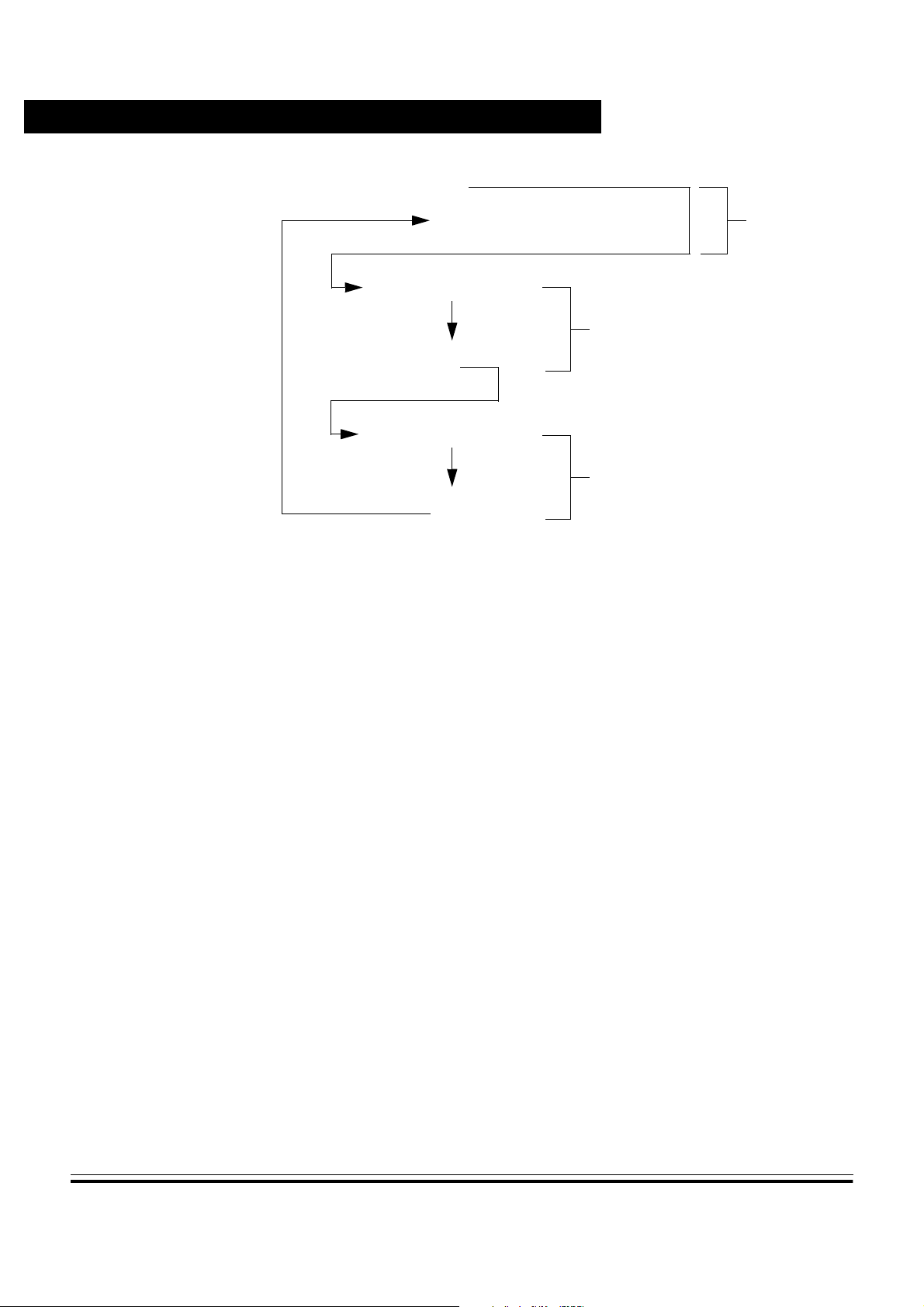
Resets and Interrupts
Freescale Semiconductor, Inc.
CLI
#$FF
LDA
INT1
INT2
nc...
I
PSHH
INT1 INTERRUPT SERVICE ROUTINE
PULH
RTI
PSHH
INT2 INTERRUPT SERVICE ROUTINE
PULH
RTI
BACKGROUND
ROUTINE
Figure 4-5. Interrupt Recognition Example
The LDA opcode is prefetched by both the INT1 and INT2 RTI
instructions. However, in the case of the INT1 RTI prefetch, this is a
redundant operation.
NOTE: To maintain compatibility with the M6805 Family, the H register is not
pushed on the stack during interrupt entry. If the interrupt service routine
modifies the H register or us es the inde xed a ddr e ssin g m ode , save the
H register and then restore it prior to exiting the routine.
cale Semiconductor,
Frees
Technical Data MC68HC908GR8 — Rev 4.0
68 Resets and Interrupts MOTOROLA
For More Information On This Product,
Go to: www.freescale.com
Freescale Semiconductor, Inc.
FROM RESET
Resets and Interrupts
Interrupts
nc...
I
cale Semiconductor,
Frees
YES
BREAK
INTERRUPT
?
NO
I BIT SET?
I BIT SET?
NO
IRQ
INTERRUPT
?
NO
CGM
INTERRUPT
?
NO
OTHER
INTERRUPTS
?
NO
FETCH NEXT
INSTRUCTION
SWI
INSTRUCTION
?
NO
RTI
INSTRUCTION
?
YES
YES
YES
YES
YES
YES
STACK CPU REGISTER S
LOAD PC WITH INTERRUPT VECTOR
UNSTACK CPU REGISTERS
SET I BIT
NO
EXECUTE INSTRUCTION
Figure 4-6. Interrupt Processing
MC68HC908GR8 — Rev 4.0 Technical Data
MOTOROLA Resets and Interrupts 69
For More Information On This Product,
Go to: www.freescale.com
Resets and Interrupts
4.4.2 Sources
The sources in Table 4-1 can generate CPU interrupt requests.
Freescale Semiconductor, Inc.
Table 4-1. Interrupt Sources
nc...
I
cale Semiconductor,
Frees
Source Flag
Reset None None None 0
SWI instruction None None None 0
IRQ
pin IRQF IMASK1 IF1 1
CGM (PLL) PLLF PLLIE IF2 2 $FFF8–$FFF9
TIM1 channel 0 CH0F CH0IE IF3 3 $FFF6–$FFF7
TIM1 channel 1 CH1F CH1IE IF4 4 $FFF4–$FFF5
TIM1 overflow TOF TOIE IF5 5 $FFF2–$FFF3
TIM2 channel 0 CH0F CH0IE IF6 6 $FFF0–$FFF1
TIM2 overflow TOF TOIE IF8 8 $FFEC–$FFED
SPI receiver full SPRF SPRIE
Mask
(1)
INT Register
Flag
Priority
(2)
$FFFE
$FFFC
$FFFA
IF9 9 $FFEA–$FFEBSPI overflow OVRF ERRIE
SPI mode fault MODF ERRIE
SPI transmitter empty SPTE SPTIE IF10 10 $FFE8–$FFE9
SCI receiver overrun OR ORIE
SCI noise fag NF NEIE
SCI framing error FE FEIE
SCI parity error PE PEIE
SCI receiver full SCRF SCRIE
SCI input idle IDLE ILIE
SCI transmitter empty SCTE SCTIE
SCI transmission complete TC TCIE
IF11 11 $FFE6–$FFE7
IF12 12 $FFE4–$FFE5
IF13 13 $FFE2–$FFE3
Vector
Address
–$FFFF
–$FFFD
–$FFFB
Keyboard pin KEYF IMASKK IF14 14 $FFDE–$FFDF
ADC conversion complete COCO AIEN IF15 15 $FFDE–$FFDF
Timebase TBIF TBIE IF16 16 $FFDC–$FFDD
Note:
1. The I bit in the condition code register is a global mask for all interrupt sources except the SWI instruction.
2. 0 = highest priority
Technical Data MC68HC908GR8 — Rev 4.0
70 Resets and Interrupts MOTOROLA
For More Information On This Product,
Go to: www.freescale.com

4.4.2.1 SWI Instruction
4.4.2.2 Break Interrupt
nc...
I
4.4.2.3 IRQ Pin
Freescale Semiconductor, Inc.
The software interrupt instruction (SWI) causes a non-maskable
interrupt.
Resets and Interrupts
Interrupts
NOTE: A software interrupt pushes PC onto the stack. An SWI does not push
PC – 1, as a hardware interrupt does.
The break modul e causes the CPU to execute an S WI instruction at a
software-pr ogrammable break point.
4.4.2.4 CGM
4.4.2.5 TIM1
cale Semiconductor,
Frees
A logic 0 on the IRQ1 pin latches an external interrupt request.
The CGM can generate a CPU interrupt request every time the phaselocked loop circuit (PLL) enters or leaves the locked state. When the
LOCK bit changes state, the PLL flag (PLLF) is set. The PLL interrupt
enable bit (PLLIE) enables PLLF CPU interrupt requests. LOCK is in the
PLL bandwidth control register. PLLF is in the PLL control register.
TIM1 CPU interrupt sources:
• TIM1 overflow flag (TOF) — The TOF bit is set when the TIM1
counter value rolls over to $0000 after matching the value in the
TIM1 counter modulo registers. The TIM1 overflow interrupt
enable bit, TOIE, enables TIM1 overflow CPU interrupt re qu ests.
TOF and TOIE are in the TIM1 status and control register.
• TIM1 channel flags (CH1F–CH0F) — The C HxF bit is set when an
input capture or out put compare occurs on cha nnel x. The channel
x interrupt enable bit, CHxIE, enables channel x TIM1 CPU
interrupt requests. CHxF and CHxIE are in the TIM1 channel x
status and control register.
MC68HC908GR8 — Rev 4.0 Technical Data
MOTOROLA Resets and Interrupts 71
For More Information On This Product,
Go to: www.freescale.com

Resets and Interrupts
4.4.2.6 TIM2
nc...
I
Freescale Semiconductor, Inc.
TIM2 CPU interrupt sources:
• TIM2 overflow flag (TOF) — The TOF bit is set when the TIM2
• TIM2 channel flag (CH0F) — The CH0F bit is set when an input
counter value rolls over to $0000 after matching the value in the
TIM2 counter modulo registers. The TIM2 overflow interrupt
enable bit, TOIE, enables TIM2 overflow CPU interrupt re qu ests.
TOF and TOIE are in the TIM2 status and control register.
capture or output compare occurs on channel 0. The channel 0
interrupt enable bit, CH0IE, enables channel 0 TIM2 CPU interrupt
requests. CH0F and CH0IE ar e in the TIM 2 channe l 0 status and
control register.
cale Semiconductor,
Frees
4.4.2.7 SPI
SPI CPU interrupt sources:
• SPI receiver full bit (SPRF) — The SPRF bit is set every time a
byte transfers from the shift register to the receive data register.
The SPI receiver interrupt enable bit, SPRIE, enables SPRF CPU
interrupt requests. SPRF is in the SPI status and control register
and SPRIE is in the SPI control register.
• SPI transmitter empty (SPTE) — The SPTE bi t is set every time a
byte transfers from the transmit data register to the shift register.
The SPI transmit inte rrupt en able bit, SP TIE, enab les SPTE CPU
interrupt req uests. SPTE is in the SPI status and c ontrol register
and SPTIE is in the SPI control register.
• Mode fault bit (MODF) — The MODF bit is set in a slave SPI if the
SS pin goes high during a transmissi on with the mode fault enable
bit (MODFEN) set. In a master SPI, the MODF bit is set if the SS
pin goes low at any time with the MODFEN bit set. The error
interrupt enable bit, ERRIE, enables MODF CPU interrupt
requests. MODF, MODFEN, and ERRIE are in the SPI status and
control register.
Technical Data MC68HC908GR8 — Rev 4.0
72 Resets and Interrupts MOTOROLA
For More Information On This Product,
Go to: www.freescale.com

nc...
I
4.4.2.8 SCI
Freescale Semiconductor, Inc.
• Overflow bit (OVRF) — The OVRF bit is set if software does not
SCI CPU interrupt sources:
• SCI transmitter empty bit (SCTE) — SCTE is set when the SCI
Resets and Interrupts
Interrupts
read the byte in the receive data register before the next full byte
enters the shift register. The error interrupt enable bit, ERRIE,
enables OVRF CPU interrupt requests. OVRF and ERRIE are in
the SPI status and control register.
data register transfers a character to the transmit shift register.
The SCI transmit in terr up t enable bit, SCTIE, en ab les transmitter
CPU interrupt reque sts. SCTE is in SCI status register 1. SCTIE is
in SCI control register 2.
cale Semiconductor,
Frees
• Transmission complete bit (TC) — TC is set when the transmit
shift register an d the S CI data re gister are emp ty and no break o r
idle character has been generated. The transmission complete
interrupt enable bit, TCIE, enables transmitter CPU interrupt
requests. TC is in SCI status register 1. TCIE is in SCI control
register 2.
• SCI receiver full bit (SCRF) — SCRF is set when the receive shift
register transfers a character to the SCI data register. The SCI
receive interrupt enable bit, SCRIE, enables receiver CPU
interrupts. SCRF is in SCI status register 1. SCRIE is in SCI
control register 2.
• Idle input bit (IDLE) — IDLE is set when 10 or 11 consecutive logic
1s shift in from the RxD pin. The idle line interrupt enable bit, ILIE,
enables IDLE CPU interrupt requests. IDLE is in SCI status
register 1. ILIE is in SCI control register 2.
• Receiver overrun bit (OR) — OR is set when the receive shift
register shifts in a new character before the previous character
was read from the SCI data regi ster. The over run interr upt enable
bit, ORIE, enables OR to generate SCI error CPU interrupt
requests. OR is in SCI status register 1. ORIE is in SCI control
register 3.
MC68HC908GR8 — Rev 4.0 Technical Data
MOTOROLA Resets and Interrupts 73
For More Information On This Product,
Go to: www.freescale.com

Resets and Interrupts
nc...
I
Freescale Semiconductor, Inc.
• Noise flag (NF) — NF is set when the SCI detects noise on
• Framing error bit (FE) — FE is set when a logic 0 occurs where the
• Parity error bit (PE) — PE is set when the SCI detects a parity error
incoming data or break characters, including start, data, and stop
bits. The noise error interrupt enable bit, NEIE, enables NF to
generate SCI error CPU interrupt requests. NF is in SCI status
register 1. NEIE is in SCI control register 3.
receiver expects a stop bit. The framing error interrupt enable bit,
FEIE, enables FE to generate SCI error CPU interrupt requests.
FE is in SCI status register 1. FEIE is in SCI control register 3.
in incoming data. The parity error interrupt enable bit, PEIE,
enables PE to generate SCI error CPU interrupt requests. PE is in
SCI status register 1. PEIE is in SCI control register 3.
4.4.2.9 KBD0–KBD4 Pins
A logic 0 on a keyboard interrupt pin latches an external interrupt
4.4.2.10 ADC (Analog-to-Digital Converter)
request.
When the AIEN bit is set, the ADC module is capable of generating a
CPU interrupt after each ADC conversion. The COCO/IDMAS bit is not
used as a conversion complete flag when interrupts are enabled.
cale Semiconductor,
4.4.2.11 TBM (Timebase Module)
The timebase module can interrupt the CPU on a regular basis with a
Frees
rate defined by TBR2–TBR0. When the timebase counter chain rolls
over, the TBIF flag is set. If the TBIE bit is set, enabling the timebase
interrupt, the counter chain overflow will generate a CPU interrupt
request.
Interrupts must b e acknowledged by writing a logic 1 to the TACK bit.
Technical Data MC68HC908GR8 — Rev 4.0
74 Resets and Interrupts MOTOROLA
For More Information On This Product,
Go to: www.freescale.com

4.4.3 Interrupt Status Registers
nc...
I
Freescale Semiconductor, Inc.
Resets and Interrupts
Interrupts
The flags in the interrupt status registers identify maskable interrupt
sources. Table 4-2 summarizes the interrupt sources and the interrupt
status register flags that they set. The interrupt status registers can be
useful for debugging.
Table 4-2. Interrupt Source Flags
Interrupt Source Interrupt Status Register Flag
Reset —
SWI instruction —
IRQ
pin IF1
CGM (PLL) IF2
cale Semiconductor,
Frees
TIM1 channel 0 IF3
TIM1 channel 1 IF4
TIM1 overflow IF5
TIM2 channel 0 IF6
Reserved IF7
TIM2 overflow IF8
SPI receive IF9
SPI transmit IF10
SCI error IF11
SCI receive IF12
SCI transmit IF13
Keyboard IF14
ADC conversion complete IF15
Timebase IF16
MC68HC908GR8 — Rev 4.0 Technical Data
MOTOROLA Resets and Interrupts 75
For More Information On This Product,
Go to: www.freescale.com

Freescale Semiconductor, Inc.
Resets and Interrupts
4.4.3.1 Interrupt Status Register 1
Address: $FE04
Bit 7654321Bit 0
Read: IF6 IF5 IF4 IF3 IF2 IF1 0 0
Write:RRRRRRRR
Reset:00000000
R = Reserved
Figure 4-7. Interrupt Status Register 1 (INT1)
nc...
I
4.4.3.2 Interrupt Status Register 2
Address: $FE05
cale Semiconductor,
Frees
IF6–IF1 — Interrupt Flags 6–1
These flags indicate the presence of interrupt requests from the
sources shown in Table 4-2.
1 = Interrupt request prese nt
0 = No interrupt request present
Bit 1 and Bit 0 — Always read 0
Bit 7654321Bit 0
Read: IF14 IF13 IF12 IF11 IF10 IF9 IF8 IF7
Write:RRRRRRRR
Reset:00000000
R = Reserved
Figure 4-8. Interrupt Status Register 2 (INT2)
IF14–IF7 — Interrupt Flags 14–7
These flags indicate the presence of interrupt requests from the
sources shown in Table 4-2.
1 = Interrupt request prese nt
0 = No interrupt request present
Technical Data MC68HC908GR8 — Rev 4.0
76 Resets and Interrupts MOTOROLA
For More Information On This Product,
Go to: www.freescale.com

Freescale Semiconductor, Inc.
4.4.3.3 Interrupt Status Register 3
Address: $FE06
Bit 7654321Bit 0
Read: 000000IF16IF15
Write:RRRRRRRR
Reset:00000000
R = Reserved
Resets and Interrupts
Interrupts
Figure 4-9. Interrupt Status Register 3 (INT3)
nc...
I
cale Semiconductor,
Frees
IF16–IF15 — Interrupt Flags 16–15
This flag indicates the presence of an interrupt request from the
source shown in Table 4-2.
1 = Interrupt request prese nt
0 = No interrupt request present
Bits 7–2 — Always read 0
MC68HC908GR8 — Rev 4.0 Technical Data
MOTOROLA Resets and Interrupts 77
For More Information On This Product,
Go to: www.freescale.com

Resets and Interrupts
nc...
I
Freescale Semiconductor, Inc.
cale Semiconductor,
Frees
Technical Data MC68HC908GR8 — Rev 4.0
78 Resets and Interrupts MOTOROLA
For More Information On This Product,
Go to: www.freescale.com

Freescale Semiconductor, Inc.
Technical Data — MC68HC908GR8
Section 5. Analog-to-Digital Converter (ADC)
5.1 Contents
5.2 Introduction. . . . . . . . . . . . . . . . . . . . . . . . . . . . . . . . . . . . . . . .79
5.3 Features . . . . . . . . . . . . . . . . . . . . . . . . . . . . . . . . . . . . . . . . . .80
nc...
I
5.2 Introduction
cale Semiconductor,
Frees
5.4 Functional Description . . . . . . . . . . . . . . . . . . . . . . . . . . . . . . .80
5.5 Interrupts. . . . . . . . . . . . . . . . . . . . . . . . . . . . . . . . . . . . . . . . . .83
5.6 Low-Power Modes . . . . . . . . . . . . . . . . . . . . . . . . . . . . . . . . . . 83
5.7 I/O Signals . . . . . . . . . . . . . . . . . . . . . . . . . . . . . . . . . . . . . . . .83
5.8 I/O Registers. . . . . . . . . . . . . . . . . . . . . . . . . . . . . . . . . . . . . . .85
This section describes the 8-bit analog-to-digital converter (ADC).
For further information regarding analog-to-digital converters on
Motorola microcontrollers, please consult the HC08 ADC Reference
Manual, ADCRM/AD.
MC68HC908GR8 — Rev 4.0 Technical Data
MOTOROLA Analog-to-Digital Converter (ADC) 79
For More Information On This Product,
Go to: www.freescale.com

Freescale Semiconductor, Inc.
Analog-to-Digital Converter (ADC)
5.3 Features
Features of the ADC module include:
• Six channels with multiplexed input
• Linear successive approximation wi th monotonicity
• 8-bit resolutio n
• Single or continuous conversion
• Conversion complete flag or conversion complete interrupt
• Selectable ADC clock
nc...
I
5.4 Functional Description
cale Semiconductor,
Frees
The ADC provides six pins for sampling external sources at pins
PTB5/ATD5–PTB0/ATD0. An analog multiplexer allows the single ADC
converter to select one of six ADC channels as ADC volta ge in (V
V
analog-to-digital converter. When the conv ersion is completed, ADC
places the result in the ADC data register and sets a flag or generates
an interrupt. See Figure 5-1.
is converted b y the successive approximation register-based
ADIN
NOTE: References to DMA (direct-memory access) and associated functions
are only valid if the MCU has a DMA module. If the MCU has no DMA,
any DMA-related register bits should be left in their reset state for
expected MCU operation.
ADIN
).
Technical Data MC68HC908GR8 — Rev 4.0
80 Analog-to-Digital Converter (ADC) MOTOROLA
For More Information On This Product,
Go to: www.freescale.com
Freescale Semiconductor, Inc.
INTERNAL
DATA BUS
READ DDRBx
Analog-to-Digital Conver ter (ADC)
Functio nal Description
nc...
I
5.4.1 ADC Port I/O Pins
cale Semiconductor,
Frees
WRITE DDRBx
WRITE PTBx
READ PTBx
INTERRUPT
LOGIC
AIEN COCO
RESET
CONVERSION
COMPLETE
CGMXCLK
BUS CLOCK
DDRBx
PTBx
ADC DATA REGISTER
ADC
ADC CLOCK
CLOCK
GENERATOR
ADIV2–ADIV0 ADICLK
ADC
VOLTAGE IN
(V
ADIN
DISABLE
DISABLE
)
CHANNEL
SELECT
PTBx
ADC CHANNEL x
ADCH4–ADCH0
Figure 5-1. ADC Block Diagram
PTB5/ATD5–PTB0/ATD0 are general-purpose I/O (input/output) pins
that share with th e ADC ch annels. Th e chann el se lect b its de fine wh ich
ADC channel/port pin will be used as the input signal. The ADC
overrides the port I/O logic by forcing that pin as input to the ADC. The
remaining ADC channels/port pins are controlled by the port I/O logic
and can be used as general-purpose I/O. Writes to the port register or
DDR will not have any affect on the port pin that is selected by the ADC.
Read of a port pin in use by the ADC w ill return a logic 0.
MC68HC908GR8 — Rev 4.0 Technical Data
MOTOROLA Analog-to-Digital Converter (ADC) 81
For More Information On This Product,
Go to: www.freescale.com

Freescale Semiconductor, Inc.
Analog-to-Digital Converter (ADC)
5.4.2 Voltage Conversion
nc...
I
5.4.3 Conversion Time
cale Semiconductor,
5.4.4 Conversion
Frees
When the input voltag e to the A DC equals V
REFH
signal to $FF (full scale). If the input voltage equals V
converts it to $00. Input voltages between V
REFH
straight-line linear conversion. All other input voltages will result in $FF,
if greater than V
REFH
.
NOTE: Inside the ADC module, th e reference voltage, V
ADC analog power V
ground V
. Therefore, the ADC input volt age sh ould not exce ed the
DDAD
analog supply voltages
For operation, V
DDAD
separate traces
Conversion starts after a write to the ADSCR. One conversion will take
between 16 and 17 ADC clock cycles. The ADIVx and ADICLK bits
should be set to provide a 1 MHz ADC clock frequency.
Conversion time =
Number of bus cycles = conversion time x bus frequency
In continuous conversion mode, the ADC data register will be filled with
new data after each conversion. Data from the previous conversion will
be overwritten whether that data has been read or not. Conversions will
continue until the ADC O bit is cleared. Th e COCO/IDMAS bit is set after
the first conversion and will stay set until the next write of the ADC status
and control register or the next read of the ADC data register.
DDAD
; and V
is connected to the ADC analog
REFL
should be tied to the same potential as V
16 to17 ADC cycles
ADC frequency
, the ADC converts the
, the ADC
REFL
and V
is connected to the
REFH
REFL
are a
DD
via
In single conversion mode, conversion begins with a write to the
ADSCR. Only one conversion occurs between writes to the ADSCR.
Technical Data MC68HC908GR8 — Rev 4.0
82 Analog-to-Digital Converter (ADC) MOTOROLA
For More Information On This Product,
Go to: www.freescale.com

5.4.5 Accuracy and Precision
5.5 Interrupts
nc...
I
Freescale Semiconductor, Inc.
The conversion process is monotonic and has no missing codes.
When the AIEN bit is set, the ADC module is capable of generating CPU
interrupts after each ADC conversion. A CPU interrupt is generated if the
COCO/IDMAS bit is at logic 0. If COCO/IDMAS bit is set, a DMA interrupt
is generated. The COCO/IDMAS bit is not used as a conversion
complete flag when interrupts are enabled.
Analog-to-Digital Conver ter (ADC)
Interrupts
5.6 Low-Power Modes
5.6.1 Wait Mode
cale Semiconductor,
5.6.2 Stop Mode
Frees
The WAIT and STOP instruction can put the MCU in low powerconsumption st andby modes.
The ADC continues normal operation during wait mode. Any enabled
CPU interrupt request from the ADC can bring th e MCU out of wait
mode. If the ADC is not required to bring the MCU out of wait mode,
power down the ADC by setting ADCH4–ADCH0 bits in the ADC status
and control register before executing the WAIT instruction.
The ADC module is inactive after the execution of a S T OP instruction.
Any pending conversion is aborted. ADC conversions resume when the
MCU exits stop mode after an external interrupt. Allow one conversion
cycle to stabilize the analog circuitry.
5.7 I/O Signals
The ADC module has six pins shared with port B,
PTB5/AD5–PTB0/ATD0.
MC68HC908GR8 — Rev 4.0 Technical Data
MOTOROLA Analog-to-Digital Converter (ADC) 83
For More Information On This Product,
Go to: www.freescale.com

Freescale Semiconductor, Inc.
Analog-to-Digital Converter (ADC)
5.7.1 ADC Analog Power Pin (V
NOTE: For maximum noise immunity, route V
5.7.2 ADC Analog Ground Pin (V
nc...
I
NOTE: Route V
5.7.3 ADC Voltage In (V
cale Semiconductor,
)/ADC Voltage Reference High Pin (V
DDAD
The ADC analog portion uses V
V
necessary to ensure clean V
pin to the same voltage potential as VDD. External filtering may be
DDAD
DDAD
as its power pin. Connect the
DDAD
for good results.
DDAD
carefully and p lace bypass
capacitors as close as possible to the package.
)/ADC Voltage Reference Low Pin (V
SSAD
The ADC analog portion uses V
V
V
pin to the same voltage potential as VSS.
SSAD
cleanly to avoid any offset errors.
SSAD
)
ADIN
is the input voltage signal fro m one of the six ADC channels to the
ADIN
as its ground pi n. Connect the
SSAD
ADC module.
REFH
REFL
)
)
Frees
Technical Data MC68HC908GR8 — Rev 4.0
84 Analog-to-Digital Converter (ADC) MOTOROLA
For More Information On This Product,
Go to: www.freescale.com

Freescale Semiconductor, Inc.
5.8 I/O Registers
These I/O registers control and monitor ADC operation:
• ADC status and control register (ADSCR)
• ADC data register (ADR)
• ADC clock register (ADCLK)
5.8.1 ADC Status and Control Register
Function of the ADC status and control register (ADSCR) is described
nc...
I
here.
Address: $0003C
Analog-to-Digital Conver ter (ADC)
I/O Registers
cale Semiconductor,
Frees
Bit 7654321Bit 0
Read:
Write:
Reset:00011111
COCO/IDMAS — Conversions Complete/Interrupt DMA Select Bit
COCO/
IDMAS
Figure 5-2. ADC Status and Control Register (ADSCR)
When the AIEN bit is a logic 0, the COCO/IDMAS is a read-only bit
which is set each time a conversion is completed except in the
continuous conversion mode wh ere it is se t after th e first conver sion.
This bit is cleared whenever the ADSCR is written or whenever the
ADR is read.
If the AIEN bit is a logic 1 , the COCO/IDMAS is a read /write bit which
selects either CPU or DMA to service the ADC interrupt request.
Reset clears this bit.
1 = Conversion completed (AIEN = 0)/DMA interrupt (AIEN = 1)
0 = Conversion not completed (AIEN = 0)/CPU interru pt (AIEN = 1)
AIEN ADCO ADCH4 ADCH3 ADCH2 ADCH1 ADCH0
CAUTION: Because the MC68HC908GR8 does NOT have a DMA module, the
IDMAS bit should NEVER be set when AIEN is set. Doing so will mask
ADC interrupts and cause unwanted results.
MC68HC908GR8 — Rev 4.0 Technical Data
MOTOROLA Analog-to-Digital Converter (ADC) 85
For More Information On This Product,
Go to: www.freescale.com

Freescale Semiconductor, Inc.
Analog-to-Digital Converter (ADC)
AIEN — ADC Interrupt Enable Bit
When this bit is set, an interrupt is generated at the end of an ADC
conversion. The interrupt signal is cleared when the data register is
read or the sta tus/control r egister is w ritten. Reset clears the AI EN bit.
1 = ADC interrupt enabled
0 = ADC interrupt disabled
ADCO — ADC Continuous Conversion Bit
When this bit is set, the ADC will convert samples continuously and
update the ADR re gister at the end of each conversion. Only one
conversion is completed between writes to the ADSCR when this bit
nc...
I
is cleared. Reset clears the ADCO bit.
1 = Continuous ADC conversion
0 = One ADC conversion
cale Semiconductor,
Frees
ADCH4–ADCH0 — ADC Channel Select Bits
ADCH4–ADCH0 form a 5-bit field which is used to select one of 16
ADC channels. Only six channels, AD5–AD0, are avail able on this
MCU. The channels are detailed in Table 5-1. Care should be take n
when using a port pin as both an analog and digital input
simultaneously to prevent switching noise from corrupting the analog
signal. See Table 5-1.
The ADC subsystem is turned off when the channel select bits are all
set to 1. This feature allows for reduced power consumption for the
MCU when the ADC is not being used.
NOTE: Recovery from the disabled state requires one conversion cycle to
stabilize.
The voltage levels supplied from internal reference nodes, as specified
in Table 5-1, are used to verify the operation of the ADC converter both
in production test and for user applications.
Table 5-1. Mux Channel Select
ADCH4 ADCH3 ADCH2 ADCH1 ADCH0 Input Select
00000 PTB0/ATD0
00001 PTB1/ATD1
00010 PTB2/ATD2
Technical Data MC68HC908GR8 — Rev 4.0
86 Analog-to-Digital Converter (ADC) MOTOROLA
For More Information On This Product,
Go to: www.freescale.com
Freescale Semiconductor, Inc.
Analog-to-Digital Conver ter (ADC)
I/O Registers
Table 5-1. Mux Channel Select
ADCH4 ADCH3 ADCH2 ADCH1 ADCH0 Input Select
00011 PTB3/ATD3
00100 PTB4/ATD4
00101 PTB5/ATD5
00110 Reserved
00111 Reserved
↓↓↓↓↓ Reserved
11011 Reserved
11100 Reserved
nc...
I
5.8.2 ADC Data Register
cale Semiconductor,
Frees
11101
11110
1 1 1 1 1 ADC power off
NOTE: If an unknown ch annel is selected it should be made clea r what value the user will read
from the ADC Data Register, unknown or reserved is not specific enough.
V
REFH
V
REFL
One 8-bit result register, ADC data register (ADR), is provided. This
register is updat ed each time an ADC conversion completes.
Address: $0003D
Bit 7654321Bit 0
Read: AD7 AD6 AD5 AD4 AD3 AD2 AD1 AD0
Write:
Reset:00000000
= Unimplemented
Figure 5-3. ADC Data Register (ADR)
MC68HC908GR8 — Rev 4.0 Technical Data
MOTOROLA Analog-to-Digital Converter (ADC) 87
For More Information On This Product,
Go to: www.freescale.com
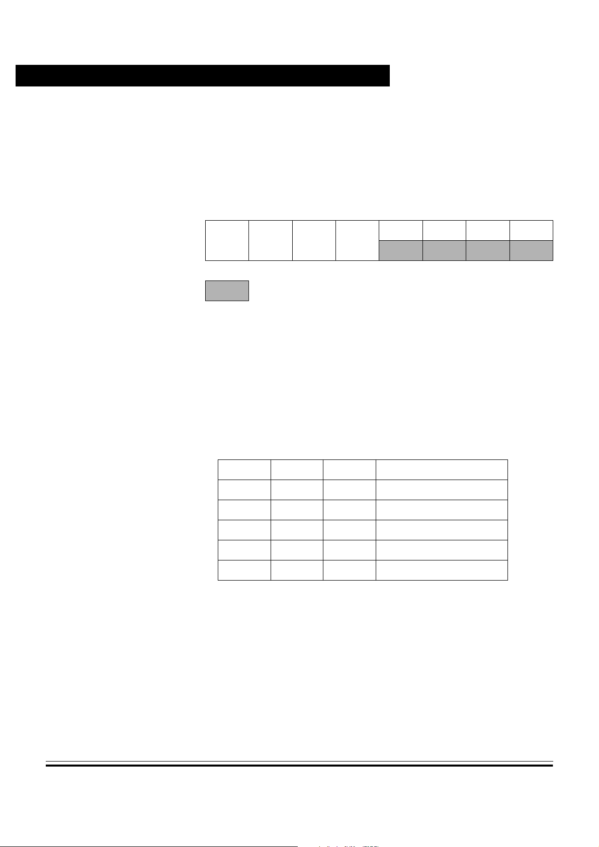
Freescale Semiconductor, Inc.
Analog-to-Digital Converter (ADC)
5.8.3 ADC Clock Register
The ADC clock register (ADCLK) selects the clock frequency for the
ADC.
Address: $0003E
Bit 7654321Bit 0
nc...
I
cale Semiconductor,
Frees
Read:
ADIV2 ADIV1 ADIV0 ADICLK
Write:
Reset:00000000
= Unimplemented
0000
Figure 5-4. ADC Clock Register (ADCLK)
ADIV2–ADIV0 — ADC Clock Prescaler Bits
ADIV2–ADIV0 form a 3-bit field which selects the divid e ratio used by
the ADC to generate the internal ADC clock. Table 5-2 shows the
approximately 1 MHz.
Table 5-2. ADC Clock Divide Ratio
ADIV2 ADIV1 ADIV0 ADC Clock Rate
available clock configurations. The ADC clock should be set to
0 0 0 ADC input clock
0 0 1 ADC input clock ÷ 2
0 1 0 ADC input clock
0 1 1 ADC input clock
1 X X ADC input clock ÷ 16
X = don’t care
÷ 1
÷ 4
÷ 8
ADICLK — ADC Input Clock Select Bit
ADICLK selects either the bus clock o r CGMXCLK as the inp ut clock
source to generate the internal ADC clock. Reset selects CGMXCLK
as the ADC clock source.
Technical Data MC68HC908GR8 — Rev 4.0
88 Analog-to-Digital Converter (ADC) MOTOROLA
For More Information On This Product,
Go to: www.freescale.com

Freescale Semiconductor, Inc.
If the external clock (CGMXCLK) is equal to or greater than 1 MHz,
CGMXCLK can be used as the clock source for the ADC. If
CGMXCLK is less than 1 MHz, use the PLL-generated bus clock as
the clock source. As long as the internal ADC clock is at
approximately 1 MHz, correct operation can be guaranteed.
1 = Internal bus clock
0 = External clock (CGMXCLK)
nc...
I
ADC input clock frequency
----------------------------------------------------------------------- 1 M H z=
ADIV2 ADIV0–
Analog-to-Digital Conver ter (ADC)
I/O Registers
cale Semiconductor,
Frees
MC68HC908GR8 — Rev 4.0 Technical Data
MOTOROLA Analog-to-Digital Converter (ADC) 89
For More Information On This Product,
Go to: www.freescale.com

Freescale Semiconductor, Inc.
Analog-to-Digital Converter (ADC)
nc...
I
cale Semiconductor,
Frees
Technical Data MC68HC908GR8 — Rev 4.0
90 Analog-to-Digital Converter (ADC) MOTOROLA
For More Information On This Product,
Go to: www.freescale.com

Freescale Semiconductor, Inc.
Technical Data — MC68HC908GR8
6.1 Contents
6.2 Introduction. . . . . . . . . . . . . . . . . . . . . . . . . . . . . . . . . . . . . . . .91
6.3 Features . . . . . . . . . . . . . . . . . . . . . . . . . . . . . . . . . . . . . . . . . .91
Section 6. Break Module (BRK)
nc...
I
6.2 Introduction
6.3 Features
cale Semiconductor,
Frees
6.4 Functional Description . . . . . . . . . . . . . . . . . . . . . . . . . . . . . . .92
6.5 Low-Power Modes . . . . . . . . . . . . . . . . . . . . . . . . . . . . . . . . . . 94
6.6 Break Module Registers. . . . . . . . . . . . . . . . . . . . . . . . . . . . . .94
This section des cribes the break module. The break module can
generate a break interrupt that stops normal program flow at a defined
address to enter a background program.
Features of the break module include:
• Accessible input/output (I/O) registers during the break interrupt
• CPU-generated break interrupts
• Software-generated break interrupts
• COP disabling during break interrupts
MC68HC908GR8 — Rev 4.0 Technical Data
MOTOROLA Break Module (BRK) 91
For More Information On This Product,
Go to: www.freescale.com

Break Module (BRK)
6.4 Functional Description
nc...
I
Freescale Semiconductor, Inc.
When the internal address bus matches the value written in the break
address registers, the break module issues a breakpoint signal to the
CPU. The CPU then loads the instruction register with a software
interrupt instructio n (SWI) after completion of the curr ent CPU
instruction. The program counter vectors to $FFFC and $FFFD ($FEFC
and $FEFD in monitor mode).
The following events can cause a break interrupt to occur:
• A CPU-generated address (the address in the program counter)
matches the contents of the break address registers.
• Software writes a logic 1 to the BRKA bit in the break status and
control register.
cale Semiconductor,
Frees
When a CPU-generated address matches the contents of the break
address registers, th e break interrupt b egins after the CPU com pletes its
current instruction. A return-from-interrupt instruction (RTI) in the break
routine ends the break interrupt and returns the MCU to normal
operation. Figure 6-1 shows the structure of the break module.
IAB15–IAB8
BREAK ADDRESS REGISTER HIGH
8-BIT COMPARATOR
IAB15–IAB0
8-BIT COMPARATOR
BREAK ADDRESS REGIS T ER LO W
IAB7–IAB0
CONTROL
BREAK
Figure 6-1. Break Module Block Diagram
Technical Data MC68HC908GR8 — Rev 4.0
92 Break Module (BRK) MOTOROLA
For More Information On This Product,
Go to: www.freescale.com

Freescale Semiconductor, Inc.
Addr.Register Name Bit 7654321Bit 0
Read: 000100BW0
SIM Break Status Register
$FE00
(SBSR)
Write:RRRRRRNOTER
Reset:00010000
Break Module (BRK)
Functio nal Description
Read:
$FE03
$FE09
nc...
I
$FE0A
$FE0B
Note: Writing a logic 0 clears BW.
SIM Break Flag Control
Register (SBFCR)
Break Address Register
High (BRKH)
Break Address Register
Low (BRKL)
Break Status and Control
Register (BRKSCR)
Write:
Reset: 0
Read:
Write:
Reset:00000000
Read:
Write:
Reset:00000000
Read:
Write:
Reset:00000000
BCFERRRRRRR
Bit 15 14 13 12 11 10 9 Bit 8
Bit 7654321Bit 0
BRKE BRKA
Figure 6-2. I/O Register Summary
6.4.1 Flag Protection During Break Interrupts
cale Semiconductor,
The BCFE bit in the SIM break flag control register (SBFCR) enables
software to clear status bits during the break state.
000000
= Unimplemented R = Reserved
6.4.2 CPU During Break Interrupts
Frees
The CPU starts a break interrupt by:
• Loading the instruction register with the SWI instruction
• Loading the program counter with $FFFC and $FFFD ($FEFC and
$FEFD in monitor mode)
MC68HC908GR8 — Rev 4.0 Technical Data
MOTOROLA Break Module (BRK) 93
For More Information On This Product,
Go to: www.freescale.com

Freescale Semiconductor, Inc.
Break Module (BRK)
The break interrupt begins after completion of the CPU instruction in
progress. If the break address register match occurs on the last cycle of
a CPU instruction, the break interrupt begins immediately.
6.4.3 TIMI and TIM2 During Break Interrupts
A break interrupt stops the timer counters.
6.4.4 COP During Break Interrupts
nc...
I
6.5 Low-Power Modes
6.5.1 Wait Mode
cale Semiconductor,
6.5.2 Stop Mode
Frees
The COP is disabled during a break interrupt when V
the RST pin.
The WAIT and STOP instructions put the MCU in low powerconsumption st andby modes.
If enabled, the bre ak module is active i n wait mode . In the break routi ne,
the user can subtract one from the return address on the stack if SBSW
is set. See Low Power Mo des. Clear the BW bit by writing logic 0 to it.
A break interrupt causes exit from stop mode and sets the SBSW bit in
the break status register.
is present on
TST
6.6 Break Module Registers
These registers control and monitor operatio n of the break module:
• Break status and control register (BRKSCR)
• Break address register high (BRKH)
Technical Data MC68HC908GR8 — Rev 4.0
94 Break Module (BRK) MOTOROLA
For More Information On This Product,
Go to: www.freescale.com

Freescale Semiconductor, Inc.
• Break address register low (BRKL)
• SIM break status register (SBSR)
• SIM break flag control register (SBFCR)
6.6.1 Break Status and Control Register
The break status an d control registe r (BRKSCR) cont ains break modu le
enable and status bits.
Address: $FE0E
Break Module (BRK)
Break Module Registers
nc...
I
cale Semiconductor,
Frees
Bit 7654321Bit 0
Read:
BRKE BRKA
Write:
Reset:00000000
= Unimplemented
000000
Figure 6-3. Break Status and Control Register (BRKSCR)
BRKE — Break Enable Bit
This read/write bit enabl es breaks on break address register match es.
Clear BRKE by writing a logic 0 to bit 7. Reset clears the BRKE bit.
1 = Breaks enabled on 16-bit address match
0 = Breaks disabled on 16-bit address match
BRKA — Break Active Bit
This read/write status and control bit is set when a break address
match occurs. Writing a logic 1 to BRKA generates a break interrupt.
Clear BRKA by writing a logic 0 to it before exiti n g the br ea k ro uti n e.
Reset clears the BRKA bit.
1 = (When read) Break add r ess mat c h
0 = (When read) No break address match
MC68HC908GR8 — Rev 4.0 Technical Data
MOTOROLA Break Module (BRK) 95
For More Information On This Product,
Go to: www.freescale.com

Freescale Semiconductor, Inc.
Break Module (BRK)
6.6.2 Break Address Registers
The break address registers (BRKH and BRKL) contain the high and low
bytes of the desire d breakpoint address. Reset clears the bre ak address
registers.
Address: $FE09
Bit 7654321Bit 0
nc...
I
6.6.3 Break Status Register
cale Semiconductor,
Read:
Bit 15 14 13 12 11 10 9 Bit 8
Write:
Reset:00000000
Figure 6-4. Break Address Register High (BRKH)
Address: $FE0A
Bit 7654321Bit 0
Read:
Bit 7654321Bit 0
Write:
Reset:00000000
Figure 6-5. Break Address Register Low (BRKL)
The break status register (SBSR) contains a flag to indicate that a break
caused an exit from wait mode. The flag is useful in applications
requiring a return to wait mode after exiting from a break interrupt.
Frees
Address: $FE00
Bit 7654321Bit 0
Read: 000100BW0
Write:RRRRRRNOTER
Reset:00010000
Note: Writing a logic 0 clears BW. R = Reserved
Figure 6-6. SIM Break Status Register (SBSR )
Technical Data MC68HC908GR8 — Rev 4.0
96 Break Module (BRK) MOTOROLA
For More Information On This Product,
Go to: www.freescale.com

Freescale Semiconductor, Inc.
Break Module (BRK)
Break Module Registers
BW — Break Wait Bit
This read/write bit is set when a break interrupt causes an exit from
wait mode. Clear BW by writing a logic 0 to it. Reset clears BW.
1 = Break interrupt during wait mode
0 = No break interrupt during wait mode
BW can be read within the break interrupt routine. The user can modify
the return address on the stack by subtracting 1 from it. The following
code is an example.
This code works if the H register was stacked in the break interrupt
routine. Execu te this code at the end of the break interrupt routine.
nc...
I
HIBYTE EQU 5
cale Semiconductor,
Frees
LOBYTE EQU 6
; If not BW, do RTI
BRCLR BW,BSR, RETURN ;;See if wait mode or stop mode
was exited by break.
TST LOBYTE,SP ; If RETURNLO is not 0,
BNE DOLO ; then just decrement low byte.
DEC HIBYTE,SP ; Else deal with high byte also.
DOLO DEC LOBYTE,SP ; Point to WAIT/STOP opcode.
RETURN PULH
RTI
; Restore H register.
MC68HC908GR8 — Rev 4.0 Technical Data
MOTOROLA Break Module (BRK) 97
For More Information On This Product,
Go to: www.freescale.com

Freescale Semiconductor, Inc.
Break Module (BRK)
6.6.4 Break Flag Control Register
The break flag control register (SBFCR) contains a bit that enables
software to clear status bits while the MCU is in a brea k state.
Address: $FE03
Bit 7654321Bit 0
Read:
Write:
Reset: 0
nc...
I
BCFE — Break Clear Flag Enable Bit
cale Semiconductor,
BCFERRRRRRR
R= Reserved
Figure 6-7. SIM Break Flag Control Register (SBFCR)
This read/write bi t en ab les software to clear status bi ts by a ccessin g
status registers whil e the MCU i s in a brea k state. To clear status bit s
during the break state, the BCFE bit must be set.
1 = Status bits clearable during break
0 = Status bits not clearable during br ea k
Frees
Technical Data MC68HC908GR8 — Rev 4.0
98 Break Module (BRK) MOTOROLA
For More Information On This Product,
Go to: www.freescale.com

Freescale Semiconductor, Inc.
Technical Data — MC68HC908GR8
Section 7. Clock Generator Module (CGMC)
7.1 Contents
7.2 Introduction. . . . . . . . . . . . . . . . . . . . . . . . . . . . . . . . . . . . . . . .99
7.3 Features . . . . . . . . . . . . . . . . . . . . . . . . . . . . . . . . . . . . . . . . .100
nc...
I
7.2 Introduction
cale Semiconductor,
Frees
7.4 Functional Description . . . . . . . . . . . . . . . . . . . . . . . . . . . . . .100
7.5 I/O Signals . . . . . . . . . . . . . . . . . . . . . . . . . . . . . . . . . . . . . . .112
7.6 CGMC Registers. . . . . . . . . . . . . . . . . . . . . . . . . . . . . . . . . . .114
7.7 Interrupts. . . . . . . . . . . . . . . . . . . . . . . . . . . . . . . . . . . . . . . . .123
7.8 Special Modes . . . . . . . . . . . . . . . . . . . . . . . . . . . . . . . . . . . .123
7.9 Acquisition/Lock Time Specifications . . . . . . . . . . . . . . . . . . .125
This section describes the clock generat or modul e. The CG MC
generates the crystal clock signal, CGMXCLK, which operates at the
frequency of the crystal. The CGMC also generates the base clock
signal, CGMOUT, which is base d on ei th er the crystal clo ck divid ed by
two or the phase- locked loop ( PLL) clock, CGMV CLK, divided b y two. In
user mode, CGMOUT is the clock from which the SIM derives the
system clocks, including the bus clock, which is at a frequency of
CGMOUT/2. In monitor mo de, PTC3 determines the bu s clock. The PLL
is a fully functiona l frequency gener ator designed for use with crystals or
ceramic resonators. The PLL can generate an 8-MHz bus frequency
using a 32-kHz crystal.
MC68HC908GR8 — Rev 4.0 Technical Data
MOTOROLA Clock Generator Module (CGMC) 99
For More Information On This Product,
Go to: www.freescale.com

Freescale Semiconductor, Inc.
Clock Generator Module (CGMC)
7.3 Features
Features of the CGMC include:
• Phase-locked loop with output frequency in integer multiples of an
integer dividend of the crystal reference
• Low-frequency crystal operation with low-po wer operation and
high-output frequency resolution
• Programmable p r escaler for power-of-two increases in frequency
• Programmable hardware voltage-controlled oscillator (VCO) for
low-jitter operation
nc...
I
7.4 Functional Description
cale Semiconductor,
Frees
• Automatic bandwidth control mode for low-jitter operation
• Automatic frequency lock detector
• CPU interrupt on entry or exit from locked condition
• Configuration register bit to allow oscillator operation during stop
mode
The CGMC consists of three major submodules:
• Crystal oscillator circuit — The crystal oscillator circuit generates
the constant crystal frequency clock, CGMXCLK.
• Phase-locked loop (PLL) — The PLL generates the
programmable VCO frequency clock, CGMVCLK.
• Base clock selector circuit — This software-controlled circuit
selects either CGMXCLK divided by two or the VCO clock,
CGMVCLK, divided by two as the base clock, CGMOUT. The SIM
derives the system clocks from either CGMOUT or CGMXCLK.
Figure 7-1 shows the structure of the CGMC.
Technical Data MC68HC908GR8 — Rev 4.0
100 Clock Generator Module (CGMC) MOTOROLA
For More Information On This Product,
Go to: www.freescale.com
 Loading...