

Motorola MC14532BD, MC14532BCL Datasheet
MOTOROLA CMOS LOGIC DATA
1
MC14532B
The MC14532B is constructed with complementary MOS (CMOS)
enhancement mode devices. The primary function of a priority encoder is to
provide a binary address for the active input with the highest priority. Eight
data inputs (D0 thru D7) and an enable input (E
in)
are provided. Five outputs
are available, three are address outputs (Q0 thru Q2), one group select (GS)
and one enable output (E
out
).
• Diode Protection on All Inputs
• Supply Voltage Range = 3.0 Vdc to 18 Vdc
• Capable of Driving Two Low–power TTL Loads or One Low–Power
Schottky TTL Load over the Rated Temperature Range
MAXIMUM RATINGS* (Voltages Referenced to V
SS
)
Symbol
Parameter Value Unit
V
DD
DC Supply Voltage – 0.5 to + 18.0 V
Vin, V
out
Input or Output Voltage (DC or Transient) – 0.5 to VDD + 0.5 V
Iin, I
out
Input or Output Current (DC or Transient),
per Pin
± 10 mA
P
D
Power Dissipation, per Package† 500 mW
T
stg
Storage Temperature – 65 to + 150
_
C
T
L
Lead Temperature (8–Second Soldering) 260
_
C
*Maximum Ratings are those values beyond which damage to the device may occur.
†Temperature Derating:
Plastic “P and D/DW” Packages: – 7.0 mW/_C From 65_C To 125_C
Ceramic “L” Packages: – 12 mW/_C From 100_C To 125_C
TRUTH TABLE
Input Output
EinD7 D6 D5 D4 D3 D2 D1 D0 GS Q2 Q1 Q0 E
out
0 X X X X X X X X 0 0 0 0 0
1 0 0 0 0 0 0 0 0 0 0 0 0 1
1 1 X X X X X X X 1 1 1 1 0
1 0 1 X X X X X X 1 1 1 0 0
1 0 0 1 X X X X X 1 1 0 1 0
1 0 0 0 1 X X X X 1 1 0 0 0
1 0 0 0 0 1 X X X 1 0 1 1 0
1 0 0 0 0 0 1 X X 1 0 1 0 0
1 0 0 0 0 0 0 1 X 1 0 0 1 0
1 0 0 0 0 0 0 0 1 1 0 0 0 0
X = Don’t Care
This device contains protection circuitry to guard against damage
due to high static voltages or electric fields. However, precautions must
be taken to avoid applications of any voltage higher than maximum rated
voltages to this high-impedance circuit. For proper operation, Vin and
V
out
should be constrained to the range VSS ≤ (Vin or V
out
) ≤ VDD.
Unused inputs must always be tied to an appropriate logic voltage
level (e.g., either VSS or VDD). Unused outputs must be left open.
SEMICONDUCTOR TECHNICAL DATA
Motorola, Inc. 1995
REV 3
1/94
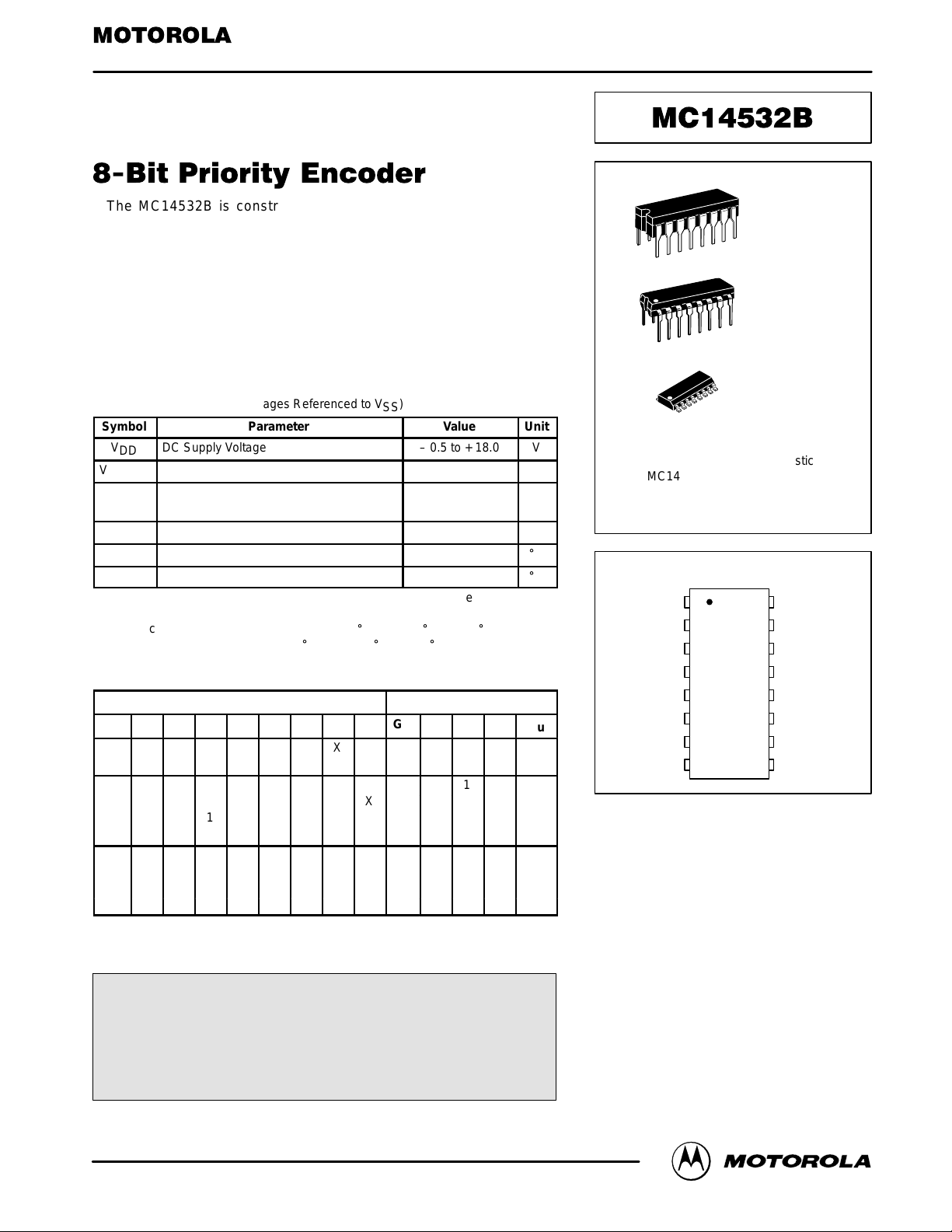
L SUFFIX
CERAMIC
CASE 620
ORDERING INFORMATION
MC14XXXBCP Plastic
MC14XXXBCL Ceramic
MC14XXXBD SOIC
TA = – 55° to 125°C for all packages.
P SUFFIX
PLASTIC
CASE 648
D SUFFIX
SOIC
CASE 751B
PIN ASSIGNMENT
13
14
15
16
9
10
11
125
4
3
2
1
8
7
6
D2
D3
GS
E
out
V
DD
Q0
D0
D1
D7
D6
D5
D4
V
SS
Q1
Q2
E
in
MOTOROLA CMOS LOGIC DATAMC14532B
2
ELECTRICAL CHARACTERISTICS (Voltages Referenced to V
SS
)
V
– 55_C 25_C 125_C
Characteristic
Symbol
V
DD
Vdc
Min Max Min Typ # Max Min Max
Unit
“0” Level
Vin = VDD or 0
V
OL
5.0
10
15
—
—
—
0.05
0.05
0.05
—
—
—
0
0
0
0.05
0.05
0.05
—
—
—
0.05
0.05
0.05
Vdc
“1” Level
Vin = 0 or V
DD
V
OH
5.0
10
15
4.95
9.95
14.95
—
—
—
4.95
9.95
14.95
5.0
10
15
—
—
—
4.95
9.95
14.95
—
—
—
Vdc
“0” Level
(VO = 4.5 or 0.5 Vdc)
(VO = 9.0 or 1.0 Vdc)
(VO = 13.5 or 1.5 Vdc)
V
IL
5.0
10
15
—
—
—
1.5
3.0
4.0
—
—
—
2.25
4.50
6.75
1.5
3.0
4.0
—
—
—
1.5
3.0
4.0
Vdc
“1” Level
(VO = 0.5 or 4.5 Vdc)
(VO = 1.0 or 9.0 Vdc)
(VO = 1.5 or 13.5 Vdc)
V
IH
5.0
10
15
3.5
7.0
11
—
—
—
3.5
7.0
11
2.75
5.50
8.25
—
—
—
3.5
7.0
11
—
—
—
Vdc
I
OH
5.0
5.0
10
15
– 3.0
– 0.64
– 1.6
– 4.2
—
—
—
—
– 2.4
– 0.51
– 1.3
– 3.4
– 4.2
– 0.88
– 2.25
– 8.8
—
—
—
—
– 1.7
– 0.36
– 0.9
– 2.4
—
—
—
—
mAdc
I
OL
5.0
10
15
0.64
1.6
4.2
—
—
—
0.51
1.3
3.4
0.88
2.25
8.8
—
—
—
0.36
0.9
2.4
—
—
—
mAdc
Input Current I
in
15 — ± 0.1 — ±0.00001 ± 0.1 — ± 1.0 µAdc
Input Capacitance
(Vin = 0)
C
in
— — — — 5.0 7.5 — — pF
Quiescent Current
(Per Package)
I
DD
5.0
10
15
—
—
—
5.0
10
20
—
—
—
0.005
0.010
0.015
5.0
10
20
—
—
—
150
300
600
µAdc
Total Supply Current**†
(Dynamic plus Quiescent,
Per Package)
(CL = 50 pF on all outputs, all
buffers switching)
I
T
5.0
10
15
IT = (1.74 µA/kHz) f + I
DD
IT = (3.65 µA/kHz) f + I
DD
IT = (5.73 µA/kHz) f + I
DD
µAdc
#Data labelled “Typ” is not to be used for design purposes but is intended as an indication of the IC’s potential performance.
**āThe formulas given are for the typical characteristics only at 25_C.
†To calculate total supply current at loads other than 50 pF:
IT(CL) = IT(50 pF) + (CL – 50) Vfk
where: IT is in µA (per package), CL in pF, V = (VDD – VSS) in volts, f in kHz is input frequency, and k = 0.005.
Output Voltage
Input Voltage
Output Drive Current
(VOH = 2.5 Vdc) Source
(VOH = 4.6 Vdc)
(VOH = 9.5 Vdc)
(VOH = 13.5 Vdc)
(VOL = 0.4 Vdc) Sink
(VOL = 0.5 Vdc)
(VOL = 1.5 Vdc)
MOTOROLA CMOS LOGIC DATA
3
MC14532B
SWITCHING CHARACTERISTICS* (C
L
= 50 pF, TA = 25_C)
Characteristic
Symbol V
DD
Min Typ # Max Unit
Output Rise and Fall Time
t
TLH
, t
THL
= (1.5 ns/pF) CL + 25 ns
t
TLH
, t
THL
= (0.75 ns/pF) CL + 12.5 ns
t
TLH
, t
THL
= (0.55 ns/pF) CL + 9.5 ns
t
TLH
,
t
THL
5.0
10
15
—
—
—
100
50
40
200
100
80
ns
Propagation Delay Time — Ein to E
out
t
PLH
, t
PHL
= (1.7 ns/pF) CL + 120 ns
t
PLH
, t
PHL
= (0.66 ns/pF) CL + 77 ns
t
PLH
, t
PHL
= (0.5 ns/pF) CL + 55 ns
t
PLH
,
t
PHL
5.0
10
15
—
—
—
205
110
80
410
220
160
ns
Propagation Delay Time — Ein to GS
t
PLH
, t
PHL
= (1.7 ns/pF) CL + 90 ns
t
PLH
, t
PHL
= (0.66 ns/pF) CL 57 ns
t
PLH
, t
PHL
= (0.5 ns/pF) CL + 40 ns
t
PLH
,
t
PHL
5.0
10
15
—
—
—
175
90
65
350
180
130
ns
Propagation Delay Time — Ein to Q
n
t
PLH
, t
PHL
= (1.7 ns/pF) CL + 195 ns
t
PLH
, t
PHL
= (0.66 ns/pF) CL + 107 ns
t
PLH
, t
PHL
= (0.5 ns/pF) CL + 75 ns
t
PHL
,
t
PLH
5.0
10
15
—
—
—
280
140
100
560
280
200
ns
Propagation Delay Time — Dn to Q
n
t
PLH
, t
PHL
= (1.7 ns/pF) CL + 265 ns
t
PLH
, t
PHL
= (0.66 ns/pF) CL + 137 ns
t
PLH
, t
PHL
= (0.5 ns/pF) CL + 85 ns
t
PLH
,
t
PHL
5.0
10
15
—
—
—
300
170
110
600
340
220
ns
Propagation Delay Time — Dn to GS
t
PLH
, t
PHL
= (1.7 ns/pF) CL + 195 ns
t
PLH
, t
PHL
= (0.66 ns/pF) CL + 107 ns
t
PLH
, t
PHL
= (0.5 ns/pF) CL + 75 ns
t
PLH
,
t
PHL
5.0
10
15
—
—
—
280
140
100
560
280
200
ns
*The formulas given are for the typical characteristics only at 25_C.
#Data labelled “Typ” is not to be used for design purposes but is intended as an indication of the IC’s potential performance.
Output
Under
VGS = V
DD
VDS = V
out
Sink Current
VGS = – V
DD
VDS = V
out
– V
DD
Source Current
Under
Test
D0 thru D7 EinD0 thru D6 D7 E
in
E
out
Q0XX00000111
Q2X001
1
GS
X0011
Figure 1. Typical Sink and Source
Current Characteristics
Figure 2. Typical Power Dissipation Test Circuit
SWITCH
MATRIX
EXTERNAL
POWER
SUPPLY
I
D
E
in
D0
D1
D2
D3
D4
D5
D6
D7
GS
Q2
Q1
Q0
E
out
V
out
PULSE
GENERATOR
(fo)
E
in
D0
D1
D2
D3
D4
D5
D6
D7
V
SS
V
DD
I
D
C
L
C
L
C
L
C
L
C
L
GS
Q2
Q1
Q0
E
out
0.01
µ
F
500
µ
F
E
Q1
0
0
X 0 0 0 1
X
1
1
 Loading...