

Motorola MC14531BCL, MC14531BCP, MC14531BD Datasheet
MOTOROLA CMOS LOGIC DATA
1
MC14531B
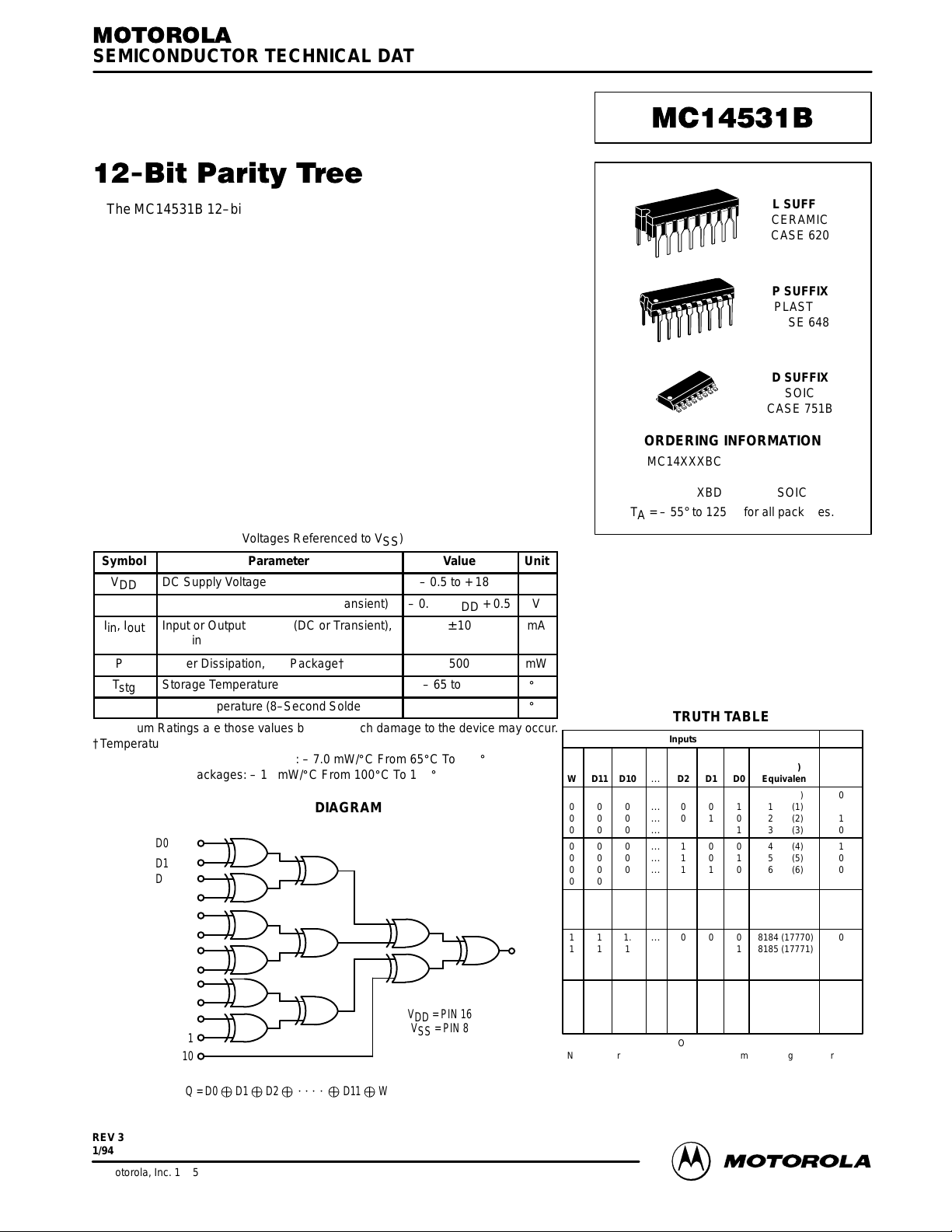
The MC14531B 12–bit parity tree is constructed with MOS P–channel and
N–channel enhancement mode devices in a single monolithic structure. The
circuit consists of 12 data–bit inputs (D0 thru D11), and even or odd parity
selection input (W) and an output (Q). The parity selection input can be
considered as an additional bit. Words of less than 13 bits can generate an
even or odd parity output if the remaining inputs are selected to contain an
even or odd number of ones, respectively . Words of greater than 12–bits can
be accommodated by cascading other MC14531B devices by using the W
input. Applications include checking or including a redundant (parity) bit to a
word for error detection/correction systems, controller for remote digital
sensors or switches (digital event detection/correction), or as a multiple input
summer without carries.
• Supply Voltage Range = 3.0 Vdc to 18 Vdc
• All Outputs Buffered
• Capable of Driving Two Low–Power TTL Loads or One Low–Power
Schottky TTL Load Over the Rated Temperature Range
• Variable Word Length
• Diode Protection on All Inputs
MAXIMUM RATINGS* (Voltages Referenced to V
SS
)
Symbol
Parameter
Value
Unit
V
DD
DC Supply Voltage
– 0.5 to + 18.0
V
Vin, V
out
Input or Output Voltage (DC or Transient)
– 0.5 to VDD + 0.5
V
Iin, I
out
Input or Output Current (DC or Transient),
per Pin
± 10
mA
P
D
Power Dissipation, per Package†
500
mW
T
stg
Storage Temperature
– 65 to + 150
_
C
T
L
Lead Temperature (8–Second Soldering)
260
_
C
*Maximum Ratings are those values beyond which damage to the device may occur.
†Temperature Derating:
Plastic “P and D/DW” Packages: – 7.0 mW/_C From 65_C To 125_C
Ceramic “L” Packages: – 12 mW/_C From 100_C To 125_C
LOGIC DIAGRAM
Q = D0 D1 D2 @@@@
D11 W
VDD = PIN 16
VSS = PIN 8
D0
D1
D2
D3
D4
D5
D6
D7
D8
D9
D10
D11
ODD/EVEN W
9 Q
7
6
5
4
3
2
1
15
14
13
12
11
10
SEMICONDUCTOR TECHNICAL DATA
Motorola, Inc. 1995
REV 3
1/94
L SUFFIX
CERAMIC
CASE 620
ORDERING INFORMATION
MC14XXXBCP Plastic
MC14XXXBCL Ceramic
MC14XXXBD SOIC
TA = – 55° to 125°C for all packages.
P SUFFIX
PLASTIC
CASE 648
D SUFFIX
SOIC
CASE 751B
TRUTH TABLE
Inputs Output
Decimal
(Octal)
W D11 D10 … D2 D1 D0 Equivalent Q*
0 0 0 … 0 0 0 0 (0) 0
0 0 0 … 0 0 1 1 (1) 1
0 0 0 … 0 1 0 2 (2) 1
0 0 0 … 0 1 1 3 (3) 0
0 0 0 … 1 0 0 4 (4) 1
0 0 0 … 1 0 1 5 (5) 0
0 0 0 … 1 1 0 6 (6) 0
0 0 0 … 1 1 1 7 (7) 1
* * * * * * * * *
* * * … * * * * *
* * * * * * * * *
1 1 1. … 0 0 0 8184 (17770) 0
1 1 1 … 0 0 1 8185 (17771) 1
1 1 1 … 0 1 0 8186 (17772) 1
1 1 1 … 0 1 1 8187 (17773) 0
1 1 1 … 1 0 0 8188 (17774) 1
1 1 1 … 1 0 1 8189 (17775) 0
1 1 1 … 1 1 0 8190 (17776) 0
1 1 1 … 1 1 1 8191 (17777) 1
*0 = Even Parity 1 = Odd Parity
NOTE:May redefine to suit application by manipulating W and/or other
available D’s.
MOTOROLA CMOS LOGIC DATAMC14531B
2
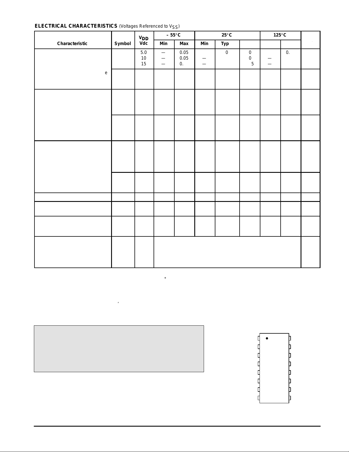
ELECTRICAL CHARACTERISTICS (Voltages Referenced to V
SS
)
V
– 55_C 25_C 125_C
Characteristic
Symbol
V
DD
Vdc
Min Max Min Typ # Max Min Max
Unit
Output Voltage “0” Level
Vin = VDD or 0
V
OL
5.0
10
15
—
—
—
0.05
0.05
0.05
—
—
—
0
0
0
0.05
0.05
0.05
—
—
—
0.05
0.05
0.05
Vdc
“1” Level
Vin = 0 or V
DD
V
OH
5.0
10
15
4.95
9.95
14.95
—
—
—
4.95
9.95
14.95
5.0
10
15
—
—
—
4.95
9.95
14.95
—
—
—
Vdc
Input Voltage “0” Level
(VO = 4.5 or 0.5 Vdc)
(VO = 9.0 or 1.0 Vdc)
(VO = 13.5 or 1.5 Vdc)
V
IL
5.0
10
15
—
—
—
1.5
3.0
4.0
—
—
—
2.25
4.50
6.75
1.5
3.0
4.0
—
—
—
1.5
3.0
4.0
Vdc
“1” Level
(VO = 0.5 or 4.5 Vdc)
(VO = 1.0 or 9.0 Vdc)
(VO = 1.5 or 13.5 Vdc)
V
IH
5.0
10
15
3.5
7.0
11
—
—
—
3.5
7.0
11
2.75
5.50
8.25
—
—
—
3.5
7.0
11
—
—
—
Vdc
Output Drive Current
(VOH = 2.5 Vdc) Source
(VOH = 4.6 Vdc)
(VOH = 9.5 Vdc)
(VOH = 13.5 Vdc)
I
OH
5.0
5.0
10
15
– 3.0
– 0.64
– 1.6
– 4.2
—
—
—
—
– 2.4
– 0.51
– 1.3
– 3.4
– 4.2
– 0.88
– 2.25
– 8.8
—
—
—
—
– 1.7
– 0.36
– 0.9
– 2.4
—
—
—
—
mAdc
(VOL = 0.4 Vdc) Sink
(VOL = 0.5 Vdc)
(VOL = 1.5 Vdc)
I
OL
5.0
10
15
0.64
1.6
4.2
—
—
—
0.51
1.3
3.4
0.88
2.25
8.8
—
—
—
0.36
0.9
2.4
—
—
—
mAdc
Input Current I
in
15 — ± 0.1 — ±0.00001 ± 0.1 — ± 1.0 µAdc
Input Capacitance
(Vin = 0)
C
in
— — — — 5.0 7.5 — — pF
Quiescent Current
(Per Package)
I
DD
5.0
10
15
—
—
—
5.0
10
20
—
—
—
0.005
0.010
0.015
5.0
10
20
—
—
—
150
300
600
µAdc
Total Supply Current**†
(Dynamic plus Quiescent,
Per Package)
(CL = 50 pF on all outputs, all
buffers switching)
I
T
5.0
10
15
IT = (0.25 µA/kHz) f + I
DD
IT = (0.50 µA/kHz) f + I
DD
IT = (0.75 µA/kHz) f + I
DD
µAdc
#Data labelled “Typ” is not to be used for design purposes but is intended as an indication of the IC’s potential performance.
**The formulas given are for the typical characteristics only at 25_C.
†To calculate total supply current at loads other than 50 pF:
IT(CL) = IT(50 pF) + (CL – 50) Vfk
where: IT is in µA (per package), CL in pF, V = (VDD – VSS) in volts, f in kHz is input frequency, and k = 0.001.
This device contains protection circuitry to guard against damage
due to high static voltages or electric fields. However, precautions must
be taken to avoid applications of any voltage higher than maximum rated
voltages to this high-impedance circuit. For proper operation, Vin and
V
out
should be constrained to the range VSS ≤ (Vin or V
out
) ≤ VDD.
Unused inputs must always be tied to an appropriate logic voltage
level (e.g., either VSS or VDD). Unused outputs must be left open.
PIN ASSIGNMENT
13
14
15
16
9
10
11
125
4
3
2
1
8
7
6
D10
D9
D8
D7
V
DD
Q
W
D11
D3
D4
D5
D6
V
SS
D0
D1
D2
 Loading...