

MOTOROLA MC10192L, MC10192FN, MC10192FNR2 Datasheet
SEMICONDUCTOR TECHNICAL DATA
3–160
REV 5
Motorola, Inc. 1996
3/93
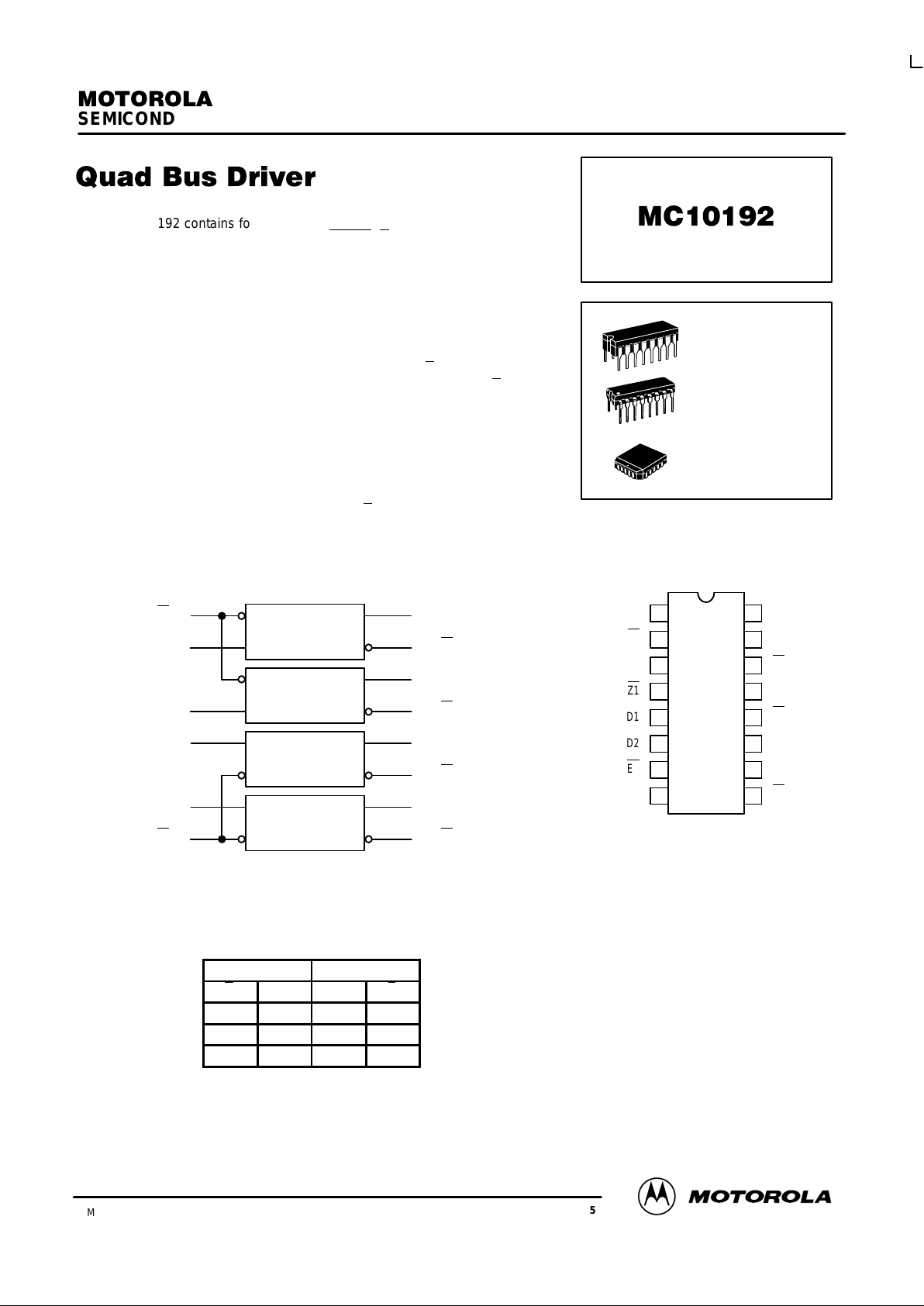
The MC10192 contains four line drivers with complementary outputs. Each
driver has a Data (D) input and shares an Enable
(E) input with another driver.
The two driver outputs are the uncommitted collectors of a pair of NPN
transistors operating as a current switch. Each driver accepts 10K MECL input
signals and provides a nominal signal swing of 800 mV across a 50 Ω load at
each output collector. Outputs can drive higher values of load resistance,
provided that the combination of IR drop and load return voltage VLR does not
cause an output collector to go more negative than –2.4 V with respect to VCC.
To avoid output transistor breakdown, the load return voltage should not be
more positive than +5.5 V with respect to VCC. When the E
input is high, both
output transistors of a driver are nonconducting. When not used, the E
inputs,
as well as the D inputs, may be left open.
Open Collector Outputs Drive Terminated Lines or
Transformers
50 kΩ Input Pulldown Resistors on All Inputs (Unused
Inputs May Be Left Open)
Power Dissipation = 575 mW typ/pkg (No Load)
Propagation Delay= 3.5 ns typ (E
— Output)
3.0 ns typ (D — Output)
LOGIC DIAGRAM
VCC= PIN 16
VEE= PIN 8
E1
7
D1
D2
D3
D4
E2
5
6
10
11
9
3
4
1
2
15
14
13
12
Z1
Z1
Z2
Z2
Z3
Z3
Z4
Z4
TRUTH TABLE
Inputs
Output
E D Z Z
H X H H
L H H L
L L L H
Note: Unused outputs must be terminated
to VCC for proper operation.
DIP
PIN ASSIGNMENT
Z2
Z2
Z1
Z1
D1
D2
E1
V
EE
V
CC
Z3
Z3
Z4
Z4
D4
D3
E2
16
15
14
13
12
11
10
9
1
2
3
4
5
6
7
8
Pin assignment is for Dual–in–Line Package.
For PLCC pin assignment, see the Pin Conversion
T ables on page 6–11 of the Motorola MECL Data
Book (DL122/D).
L SUFFIX
CERAMIC PACKAGE
CASE 620–10
P SUFFIX
PLASTIC PACKAGE
CASE 648–08
FN SUFFIX
PLCC
CASE 775–02
MC10192
3–161 MOTOROLAMECL Data
DL122 — Rev 6
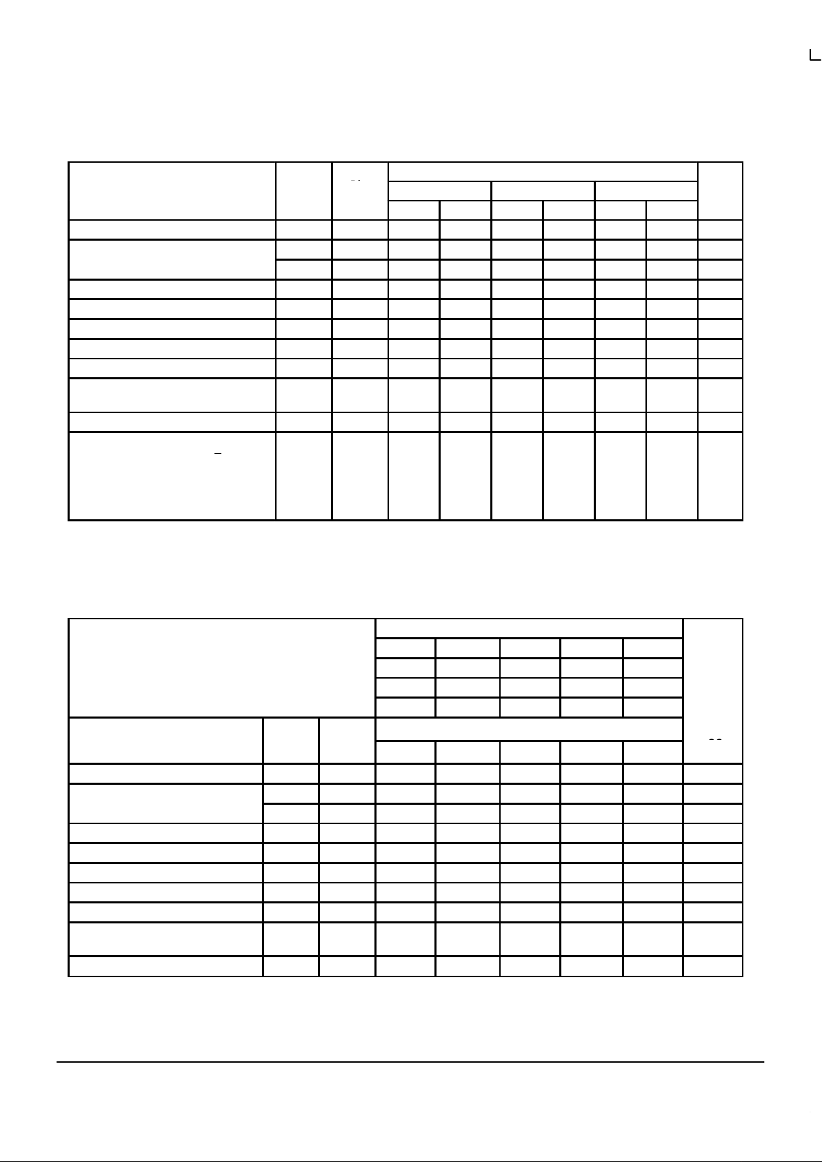
ELECTRICAL CHARACTERISTICS
Test Limits
Pin
Under
–30°C +25°C +85°C
Characteristic Symbol
Under
Test
Min Max Min Max Min Max
Unit
Power Supply Drain Current I
E
8 154 140 154 mAdc
Input Current I
inH
5 350 220 220 µAdc
I
inL
5 0.5 0.5 0.3 µAdc
Output Current High Logic 1 I
OH
2 2.0 mAdc
Output Current Low Logic 0 I
OL
2 13.5 18.0 14.0 18.0 14.0 19.0 mAdc
Threshold Current High Logic 1 I
OHC
2 2.0 2.0 2.0 mAdc
Threshold Current Low Logic 0 I
OLC
2 13.5 14.0 14.0 mAdc
Output Sink Current Low Logic 0 I
OS
2 13.3 13.9 13.3 mAdc
Load Return Voltage Absolute Max
Rating (Note 1.)
V
LR
5.5 5.5 5.5 V
Output Voltage Low (Note 2.) V
OLS
–2.4 V
Switching Times (50Ω Load) ns
Propagation Delay E to Output
D to Output
t
PHL
t
PLH
2.0
1.5
6.0
4.5
Rise/Fall Time (20 to 80%) t
TLH
t
THL
3.3
1. The 5.5V value is a maximum rating, do not exceed. A 270Ω resistor will prevent output transistor breakdown.
2. Limitations of load resistor and load return voltage combinations. Refer to page 3–160 description.
ELECTRICAL CHARACTERISTICS (continued)
TEST VOLTAGE VALUES (Volts)
@ Test Temperature V
IHmax
V
ILmin
V
IHAminVILAmax
V
EE
–30°C –0.890 –1.890 –1.205 –1.500 –5.2
+25°C –0.810 –1.850 –1.105 –1.475 –5.2
+85°C –0.700 –1.825 –1.035 –1.440 –5.2
Pin
TEST VOLTAGE APPLIED TO PINS LISTED BELOW
Characteristic Symbol
Und
er
Test
V
IHmax
V
ILmin
V
IHAminVILAmax
V
EE
(VCC)
Gnd
Power Supply Drain Current I
E
8 8 16
Input Current I
inH
5 5 8 16
I
inL
5 5 8 16
Output Current High Logic 1 I
OH
2 5,6,10,1 1 8 16
Output Current Low Logic 0 I
OL
2 5,6,10,11 8 16
Threshold Current High Logic 1 I
OHC
2 5,7,9,10,1 1 6 8 16
Threshold Current Low Logic 0 I
OLC
5,10,1 1 7,9 6 8 16
Output Sink Current Low Logic 0 I
OS
2 5,6,10,11 8 16
Load Return Voltage Absolute Max
Rating (Note 1.)
V
LR
8 16
Output Voltage Low (Note 2.) V
OLS
8 16
Each MECL 10,000 series circuit has been designed to meet the dc specifications shown in the test table, after thermal equilibrium has been
established. The circuit is in a test socket or mounted on a printed circuit board and transverse air flow greater than 500 linear fpm is maintained.
Outputs are terminated through a 50–ohm resistor to –2.0 volts. Test procedures are shown for only one gate. The other gates are tested in the
same manner.
 Loading...