


MM1165ZT
MITSMI MM1165ZT, MM1165JT, MM1165IM, MM1165IT, MM1165JM Datasheet
...
MITSUMI
Ultra-Low Power Consumption Low-Saturation Three-Pin Regulators with On/Off Pin MM1065 and 1165
Ultra-Low Power Consumption Low-Saturation Three-Pin Regulators with On/Off Pin
Monolithic ICs MM1065 and 1165
Outline
These ICs are stabilized power supply devices with ultra-low consumption currents, designed for a greatly
reduced reactive current at low input voltages, and with a small input/output difference voltage of 0.2V at an
output current of 40mA. The output current is limited to a maximum of 100mA, and in the MMP-4A package,
an on/off pin enables the device to be switched on and off.
Features
1. Input/output voltage difference 0.2V typ. (IO=40mA)
2. No-load input current 13µA typ.
3. Maximum reactive current at low input voltages 15µA typ. (no-load)
4. Maximum output current 100mA max.
5. Temperature coefficient of output voltage ±0.01%/°C typ.
6. Output voltage ranks MM1065, 1165 F : 6.0V±4%
G : 5.0V±4%
H : 4.5V±4%
I : 4.0V±4%
J : 3.0V±4%
Z : 3.3V±4%
7. With overcurrent protection circuit
8. With thermal shutdown circuit
9. With function to turn output on and off
(MMP-4A package only)
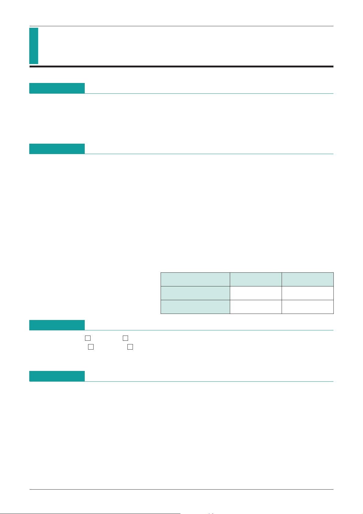
On/Off Pin Level Low High
MM1065 output ON OFF
Package
TO-92A (MM1065 T, MM1165 T)
MMP-4A (MM1065 M, MM1165 M)
The output voltage rank appears in the boxes.
*
Applications
1. Handheld computers
2. Portable transceivers
3. Cordless phones
4. Other portable equipment which uses batteries
MM1165 output OFF ON
MITSUMI
Ultra-Low Power Consumption Low-Saturation Three-Pin Regulators with On/Off Pin MM1065 and 1165
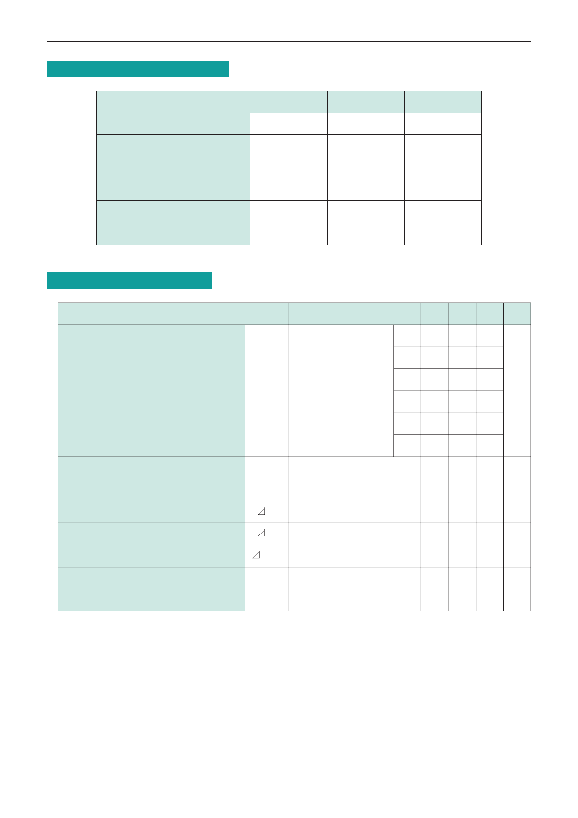
Absolute Maximum Ratings
Item Symbol Ratings Units
Operating temperature T
Storage temperature T
Power supply current V
Output current I
Maximum Ratings Pd
Electrical Characteristics
Item Symbol Measurement conditions Min. Typ. Max. Units
Output voltage Vo
OPR
STG
CC max.
OUT 100 mA
-
20~+75 °C
-
40~+125 °C
-
0.3~10 V
200 (MMP-4A)
300 (TO-92A)
F 5.76 6.00 6.24
G 4.80 5.00 5.20
IN=Vo+1V H 4.32 4.50 4.68
V
Io=40mA I 3.84 4.00 4.16
mW
V
J 2.88 3.00 3.12
Z 3.17 3.30 3.43
No-load input current Iccq1 V
Minimum I/O voltage difference Vd min. V
Input fluctuation rate V2
Load fluctuation rate V1 V
IN=Vo+1V, Io=0mA 13 20 µA
IN=Vo min., Io=40mA 0.2 0.3 V
VIN=(Vo+1V)~10V, Io=40mA
IN=Vo+1V, Io=0~100mA
±0.01 ±0.1
±0.01 ±0.03
Output voltage temperature coefficient Vo/T Tj=-20~+75°C ±100
RIPPLE=1V, VIN=Vo+2V
V
Ripple rejection rate RR
50 60 dB
f=120Hz, Io=40mA
%/V
%/mA
ppm/°C
 Loading...