

Mitac 8170 Service Manual
SERVICE MANUAL FOR
SERVICE MANUAL FOR
SERVICE MANUAL FOR
8 1 7 0
8 1 7 0
8 1 7 08 1 7 0
8 1 7 0
8 1 7 0
8 1 7 08 1 7 0
8 1 7 0
8 1 7 0
8 1 7 08 1 7 0
BY:
TESTING TECHNOLOGY DEPARTMENT / TSSC
TESTING TECHNOLOGY DEPARTMENT / TSSC
Feb . 2002
Jacey
Jacey
Liu
Liu

CONTENTS
CONTENTS
8170 N/B MAINTENANCE
1. Hardware Engineering Spec ification--------------------------------------------------------------------------------
1.1 Introduction--------------------------------------------------------------------------------------------------------------------------------
1.2 System Architecture----------------------------------------------------------------------------------------------------------------------
1.3 Electrical Characteristic-----------------------------------------------------------------------------------------------------------------
1.4 APPENDIX---------------------------------------------------------------------------------------------------------------------------------
1.5 BIOS Specification------------------------------------------------------------------------------------------------------------------------
2. System Assembly & Disassem bly ---------------------------------------------------------------------------- --------
2.1 System View--------------------------------------------------------------------------------------------------------------------------------
2.2 System Disassembly----------------------------------------------------------------------------------------------------------------------
3. Definition & Location Connectors / Switches Se tting ------------------------ -----------------------------------
3.1 Main Board---------------------------------------------------------------------------------------------------------------------------------
3.2 D/D Board-----------------------------------------------------------------------------------------------------------------------------------
3.3 Touch PAD Board-------------------------------------------------------------------------------------------------------------------------
4. Definition & Location Major Components-------------------------------------------------------------------------
4.1 Main Board---------------------------------------------------------------------------------------------------------------------------------
4.2 D/D Board----------------------------------------------------------------------------------------------------------------------------------
4
4
5
22
32
39
82
82
86
104
104
107
108
109
109
111
5. Pin Descriptions of Major Components ----------------------------------------------------------------------------
5.1 Pentium 4(Willamette/Northwood) Micro-FCPGA 478 pin----------------------------------------------------------------------
5.2 Intel 82845(Brookdale Memory Controller HUB)----------------------------------------------------------------------------------
5.3 Intel 82801BA(I/O Controller HUB )-------------------------------------------------------------------------------------------------
5.4 PCI4410(PCMCIA/1394 LINK Controller )----------------------------------------------------------------------------------------
112
112
118
125
130
1

CONTENTS
CONTENTS
8170 N/B MAINTENANCE
6. System Block Diagram -------------------------------------------------------------------------------------------------
7. Maintenance Diagnostic ----- -------------------------------------------------------------------------------------------
7.1 Introduction--------------------------------------------------------------------------------------------------------------------------------
7.2 Error Codes--------------------------------------------------------------------------------------------------------------------------------
7.3 Debug Card--------------------------------------------------------------------------------------------------------------------------------
8. Trouble Shooting ------------------ --------------------------------------------------------------------------------------
8.1 No Power------------------------------------------------------------------------------------------------------------------------------------
8.2 Battery Can not Be Charged-----------------------------------------------------------------------------------------------------------
8.3 No Display----------------------------------------------------------------------------------------------------------------------------------
8.4 VGA Controller Failure LCD No Display-------------------------------------------------------------------------------------------
8.5 VGA Controller Failure External Monitor No Display---------------------------------------------------------------------------
8.6 Memory Test Error-----------------------------------------------------------------------------------------------------------------------
8.7 Keyboard(K/B) and Touch Pad(T/B) Test Error-----------------------------------------------------------------------------------
8.8 Hard Drive Test Error-------------------------------------------------------------------------------------------------------------------
8.9 CD-ROM Drive Test Error-------------------------------------------------------------------------------------------------------------
8.10 USB Port Test Error--------------------------------------------------------------------------------------------------------------------
8.11 PIO Port Test Error---------------------------------------------------------------------------------------------------------------------
8.12 PC-Card Failure-------------------------------------------------------------------------------------------------------------------------
8.13 IEEE1394 Failure-----------------------------------------------------------------------------------------------------------------------
8.14 Audio Failure----------------------------------------------------------------------------------------------------------------------------
8.15 LAN Test Failure------------------------------------------------------------------------------------------------------------------------
136
137
137
138
140
142
143
148
151
153
155
157
159
161
163
165
167
169
171
173
176
9. Spare Parts List ----------------------------------------------------------------------------------------------------------
178
2

CONTENTS
CONTENTS
8170 N/B MAINTENANCE
10. System Explode View ------ -------------------------------------------------------------------------------------------
11. Circuit Diagram --------------------------------------------- -----------------------------------------------------------
12. Reference ---------------------------------------------------------------------------- ------------------------------------
189
190
215
3
8170 N/B MAINTENANCE
1.Hardware Engineering Specification
1.1 Introduction
1.1.1 General Description
This document describes the system hardware engineering specification for 8170 portable notebook computer system.
The 8170 notebook computer is a new mainstream high performance notebook in the MiTAC notebook family.
1.1.2 System Overview
CPU mPGA 478 -PIN Socket Support Intel Pentium (Willamette)/Northwood in mFC-PGA2 package
Video
Momory Two 144Pin SO-DIMM ,withont and on-board Memory
PCMCIA
IDE Support 2 IDE channel,Up to Ultra DMA 100
LCD Display
Button 5 Easy Start Button(functions defined by user)& 1 Mail Receive Button
LAN Support to 10/100 Based T
Modem 56Kbps V.90 MDC Modem
Pointing Glide PAD with 2 Buttons and 1 scroll button
Keyboard Internal Key Matrix Keyboard
BIOS 512KB Flash EEPROM (Include System BIOS&VGA BIOS)
1. Dual independent Displays(LCD/CRT, LCD/TV,CRT/TV)
2. Support Motion Compensation and iDCT
3. Support Simultaneous display
1. Support one slot of TypeII
2. Non Support Zoom video/Audio Function
Support Dual 85MHz LVDS interface.
Support up to QXGA(2048*1536) Resolution
4
8170 N/B MAINTENANCE
Audio 1. AC'97 Interface Codec. Sound Blaster Pro Compatible.
2. Built-In 21W speaker and 1 Mono-Microphone
I/O Port
Suspend Mode POS(S1), Suspend to RAM(S3), Suspend to Disk(S4)
Indicator HDD,FDD,CD-ROM,Num Lock,Caps Lock, Scroll Lock LEDs
1.2 System Architecture
1. Bi-Direction Parallel Port (EPP/ECP) 2. External VGA Port(D-SUB 15Pins)
3. 2 Standard USB 1.1 Port 4. SPIDF Jack
5. RJ-11 Port for Modem 6. Microphone In Jck
7. RJ-45 Port for LAN 8. VR for Audio Volume Control
9. DC Input Jack 10.Mini IEEE 1394 Port
11. S-Video Output Port(NTSC/PAL) 12. Battery Connector
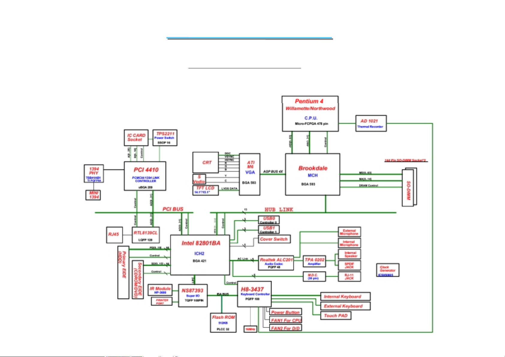
1.2.1 Block Diagram(without Power System)
5
8170 N/B MAINTENANCE
8170 System Block Diagram
6

8170 N/B MAINTENANCE
1.2.2 Function Description
1.2.2.1 CPU
Socket Intel Pentium 4/ Northwood processors with 100MHz FSB.400MHz system bus.Capable of mFC-PGA2
package
Available at 1.50, 1.60, 1.70, 1.80, 1.90 and 2 GHz
Binary compatible with applications running on previous members of the Intel microprocessor line
Intel® NetBurst™ micro-architecture
System bus frequency at 400 MHz
Rapid Execution Engine: Arithmetic Logic Units (ALUs) run at twice the processor core frequency
Hyper Pipelined Technology
Advance Dynamic Execution
---Very deep out-of-order execution
---Enhanced branch prediction
Level 1 Execution Trace Cache stores 12K micro-ops and removes decoder latency from main execution loops
8 KB Level 1 data cache
256 KB Advanced Transfer Cache (on-die,full speed Level 2 (L2) cache) with 8-way associatively and Error
Correcting Code (ECC)
144 new Streaming SIMD Extensions 2 (SSE2) instructions
Enhanced floating point and multimedia unit for enhanced video, audio,encryption, and 3D performance
Power Management capabilities
---System Management mode
---Multiple low-power states
7

8170 N/B MAINTENANCE
Optimized for 32-bit applications running on advanced 32-bit operating systems
8-way cache associatively provides improved cache hit rate on load/store operations.
1.2.2.2 CORE LOGIC
Intel Brookdale 82845 Memory Control HUB
Intel® Pentium® 4 Processor (478 pin package) Support:
---Enhanced Mode Scaleable Bus Protocol
---2x Address, 4x Data
---System Bus interrupt delivery
---400 MHz system bus
---System Bus Dynamic Bus Inversion (DBI)
---32-bit system bus addressing
---12 deep In-Order Queue
---AGTL+ bus driver technology with integrated AGTL+ termination resistors
System Memory Support
---Directly supports one SDR SDRAM channel, 64 bits wide (72 bits with ECC)
---133 MHz SDR SDRAM devices
---64 Mb, 128 Mb, 256 Mb and 512 Mb technologies for x8 and x16 devices
---By using 64 Mb technology, the smallest memory capacity possible is 32 MB
---Configurable optional ECC operation (single bit Error Correction and multiple bit Error Detection)
---Page sizes of 2 KB, 4 KB, 8 KB and 16 KB (individually selected for every row)
---Thermal management
---Maximum of 3 Double-Sided DIMMs (6rows populated) with unbuffered PC133 (with or without ECC)
---3 GB Maximum using 512 Mb technology
---Supports up to 24 simultaneous open pages
---Maximum memory bandwidth of 1.067 GB/s with PC133
8

8170 N/B MAINTENANCE
Hub Interface to Intel® 82801BA ICH2
---266 MB/s point-to-point hub interface to ICH2
---66 MHz base clock
---MSI interrupt messages, power management state change, SMI, SCI and SERR error indication
Accelerated Graphics Port (AGP) Interface
--- Supports a single AGP device (either a connector or on the motherboard)
---Supports AGP 2.0 including 1x, 2x, and 4x AGP data transfers and 2x/4x Fast Write protocol
---Supports only 1.5 V AGP electrical characteristics
---32 deep AGP request queue
---Delayed transaction support for AGP-to-System Memory FRAME# semantic reads
System Interrupt Support
---System bus interrupt delivery mechanism
---Interrupts signaled as upstream memory writes from AGP/PCI
---Supports peer MSI between hub interface and AGP
---Provides redirection for IPI and upstream interrupts to the system bus
Power Management
---SMRAM space remapping to A0000h
---Supports extended SMRAM space above 256 MB, additional TSEG from Top of Memory
interface are not supported
---PC ’99 suspend to DRAM support
---ACPI, Revision 1.0b compliant power management
---APM, Revision 1.2 compliant power management
---NT Hardware Design Guide, Version 1.0 compliant
Package
---MCH: 593 pin FC-BGA (37.5 x 37.5 mm)
9

8170 N/B MAINTENANCE
Intel 82801BA Internal Connect HUB
PCI Bus I/F
---Supports PCI at 33 MHz
---Supports PCI Rev 2.2 Specification
---133 MByte/sec maximum throughput
---Supports up to 6 master devices on PCI
---One PCI REQ/GNT pair can be given higher arbitration priority (intended for external 1394 host controller)
Integrated LAN Controller
---WfM 2.0 Compliant
---Interface to discrete LAN Connect component
---10/100 Mbit/sec Ethernet support
---1 Mbit/sec HomePNA* support
Integrated IDE Controller
---Independent timing of up to 4 drives
---Ultra ATA/100/66/33, BMIDE and PIO modes
Read transfers up to 100MB/s, Writes to 89 MB/s
---Separate IDE connections for Primary and Secondary cables
---Implements Write Ping-Pong Buffer for faster write performance
USB
---2 UHCI Host Controllers with a total of 4 ports
---USB 1.1 compliant
---Supports wake-up from sleeping states S1–S4
---Supports legacy Keyboard/Mouse software
AC'97 Link for Audio and Telephony CODECs
---AC’97 2.1 compliant
10

8170 N/B MAINTENANCE
---Independent bus master logic for 5 channels (PCM In/Out, Mic Input, Modem In/Out)
---Separate independent PCI functions for Audio and Modem
---Support for up to six channels of PCM audio output (full AC3 decode)
---Supports wake-up events
Interrupt Controller
---Support up to 8 PCI interrupt pins
---Supports PCI 2.2 Message-Based Interrupts
---Two cascaded 82C59
---Integrated I/O APIC capability
---15 interrupts supported in 8259 mode, 24 supported in I/O APIC mode
---Supports Serial Interrupt Protocol
---Supports Front-Side Bus interrupt delivery
1.8 V operation with 3.3 V I/O
---5V tolerant buffers on IDE, PCI, USB Over current and Legacy signals
GPIO
---TTL, Open-Drain, Inversion
Timers Based on 82C54
---System timer, Refresh request, Speaker tone output
Power Management Logic
---ACPI 1.0 compliant
---ACPI Power Management Timer
---PCI PME# support
---SMI# generation
---All registers readable/restorable for proper resume from 0V suspend states
---Support for APM-based legacy power management for non-ACPI implementations
11

8170 N/B MAINTENANCE
External Glue Integration
---Integrated Pull-up, Pull-down and Series Termination resistors on IDE and processor interface
Enhanced Hub I/F buffers improve routing flexibility (Not available with all Memory Controller Hubs)
Firmware Hub (FWH) I/F supports BIOS memory size up to 8 MBs
Low Pin count (LPC) I/F
---Allows connection of legacy ISA and X-Bus devices such as Super I/O
---Supports two Master/DMA devices.
Enhanced DMA Controller
---Two cascaded 8237 DMA controllers
---PCI DMA: Supports PC/PCI — Includes two PC/PCI REQ#/GNT# pairs
---Supports LPC DMA
---Supports DMA Collection Buffer to provide Type-F DMA performance for all DMA channels
Real-Time Clock
---256-byte battery-backed CMOS RAM
---Hardware implementation to indicate century rollover
System TCO Reduction Circuits
---Timers to generate SMI# and Reset upon detection of system hang
---Timers to detect improper processor reset
---Integrated processor frequency strap logic
SM Bus
---Host interface allows processor to communicate via SM Bus
---Slave interface allows an external Micro controller to access system resources
---Compatible with most 2-Wire components that are also I2C compatible
12

8170 N/B MAINTENANCE
Supports ISA bus via external PCI-ISA Bridge
360-pin EBGA package
1.2.2.3 Memory
64MB PC133 SDRAM SO-DIMM Expandable to 1024MB(2 SODIMM slots).
Support 3.3V PC133 SDR SDRAM only.
Table 1.1 MEMORY EXPANSION CAPACITY
Slot1 Slot2 Total
64MB
0
64MB
64MB 32MB 96MB
64MB 64MB 128MB
64MB 128MB 192MB
64MB 256MB 320MB
64MB 512MB 576MB
128MB 128MB 256MB
128MB 256MB 384MB
128MB 512MB 640MB
256MB 256MB 512MB
256MB 512MB 768MB
512MB 512MB 1024MB
1
54 pin or
50 pin
TSOP
67.6mm ( 2.66”)
54 pin or
50 pin
TSOP
59 61
54 pin or
50 pin
TSOP
SPD
54 pin or
50 pin
TSOP
Figure 1.1 SO-DIMM MODULE
31.75mm
(1.25”)
143
13

8170 N/B MAINTENANCE
1.2.2.4 I/O Ports
• CRT Port
@ Standard VGA compatible port
@ DDC1 and DDC2B compliant
Table 1.2 CRT CONNECTOR
PIN SIGNAL DESCRIPTION
1
2
3
4
5
6
7
8
9
10
11
12
13
14
15
RED Red analog video output
GREEN Green analog video output
BLUE Blue analog video output
Monitor Sense Monitor Sense
GN D Ground
GN D Ground
GN D Ground
GN D Ground
VCC +5VDC
GN D Ground
Monitor Sense Monitor Sense
CRT DATA Data from DDC monitor
HSYNC Horizontal Sync Control
VSYNC Vertical Sync control
CRT CLK Clock to DDC monitor
12345
10
Figure 1.2 CRT CONNECTOR
6
1112131415
14
8170 N/B MAINTENANCE
• Standard 4 Pins S-VIDEO Port for TV-Out
@ Support 1024*768 resolution
@ Support 848*480 resolution in 16:9 mode
@ Support PAL and NTSC system
Table 1.3 S-VIDEO CONNECTOR
PIN SIGNAL DESCRIPTION
1
2
3
4
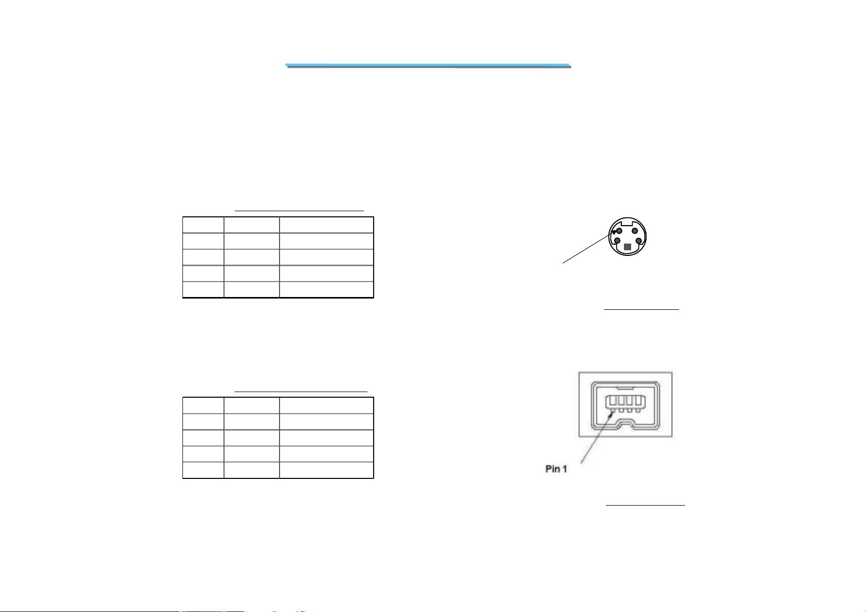
• IEEE1394 Port
GND -
GND LUMA O
CRMA O
Pin 1
Figure1.3 S-VIDEO Port
Table 1.4 IEEE1394 CONNECTOR
PIN SIGNAL DESCRIPTION
1
2
3
4
TPB- I/O
TPB+ I/O
TPA- I/O
TPA+ I/O
• AUDIO Ports
@ Built in 1 mono microphone
Figure1.4 IEEE1394 Port
15

8170 N/B MAINTENANCE
@ SPDIF
@ Microphone In
• RJ11
@ Connection to Modem Daughter Board connector
Table 1.5 MODEM CONNECTOR
PIN SIGNAL NAME DIRECTION DESCRIPTION
1 NC - No Connect
2 LINE+ I/O Phone Line Positive
3 LIN E- I/O Phone Line Negative
4 NC - No C onnect
Figure 1.5 MODEM Port
• RJ45
@ Connection to on-board NIC controller
Table 1.6 LAN CONNECTOR
PIN SIGNAL NAME DIRECTION DESCRIPTION
1 TX+ Out Transmit Data Ring
2 TX- Out Transmit Data Tip
3 RX+ IN Receive Data Ring
4 TERM 1 - Internal termination resistor
5 TEMR 2 - Internal termination resistor
6RX IN Receive Data Tip
7 TERM 3 - Internal termination resistor
8 TERM 4 - Internal termination resistor
Figure 1.6 LAN CONNECTOR
16
8170 N/B MAINTENANCE
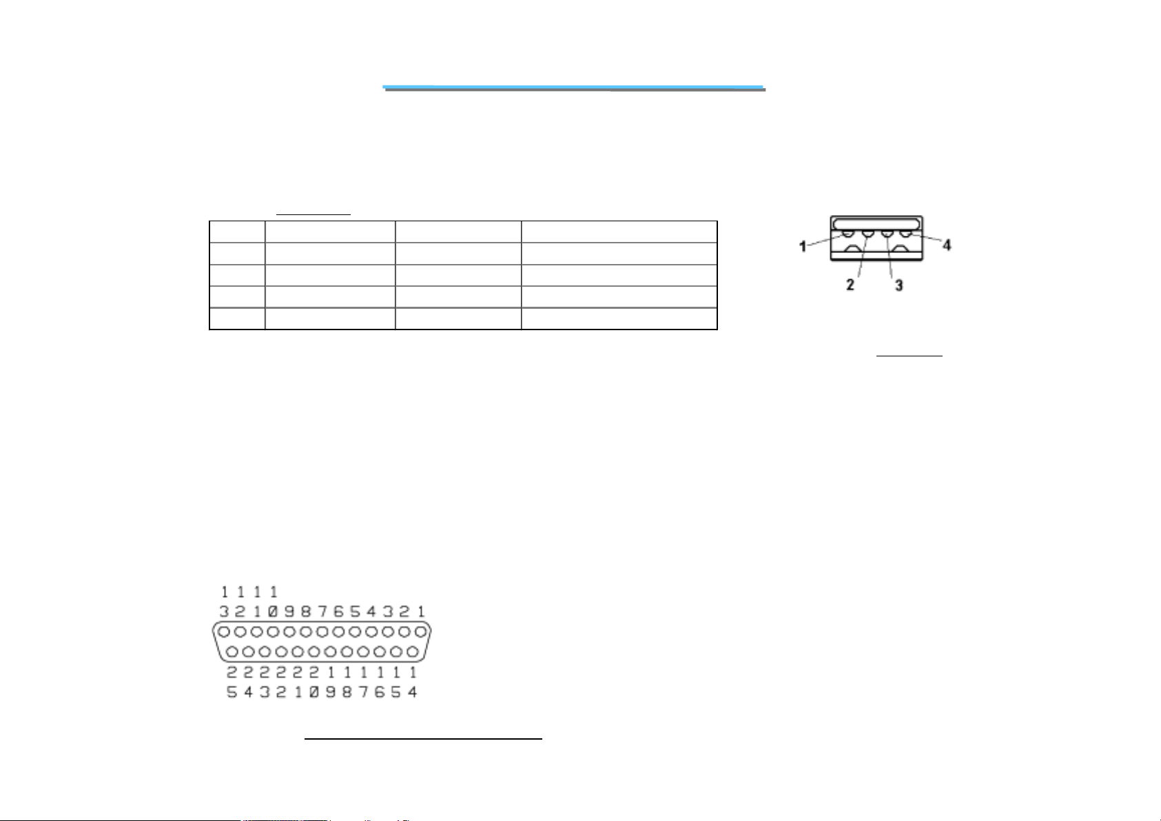
• USB Port
@ Two industry standard USB 1.1 ports
Table 1.7 USB Port2
PIN SIGNAL NAME DIRECTION DESCRIPTION
1 VCC - USB Device Power (+5VDC)
2 DATA- I/O Balanced Data Negaitve
3 DATA+ I/O Balanced Data Posiitve
4GND - Ground
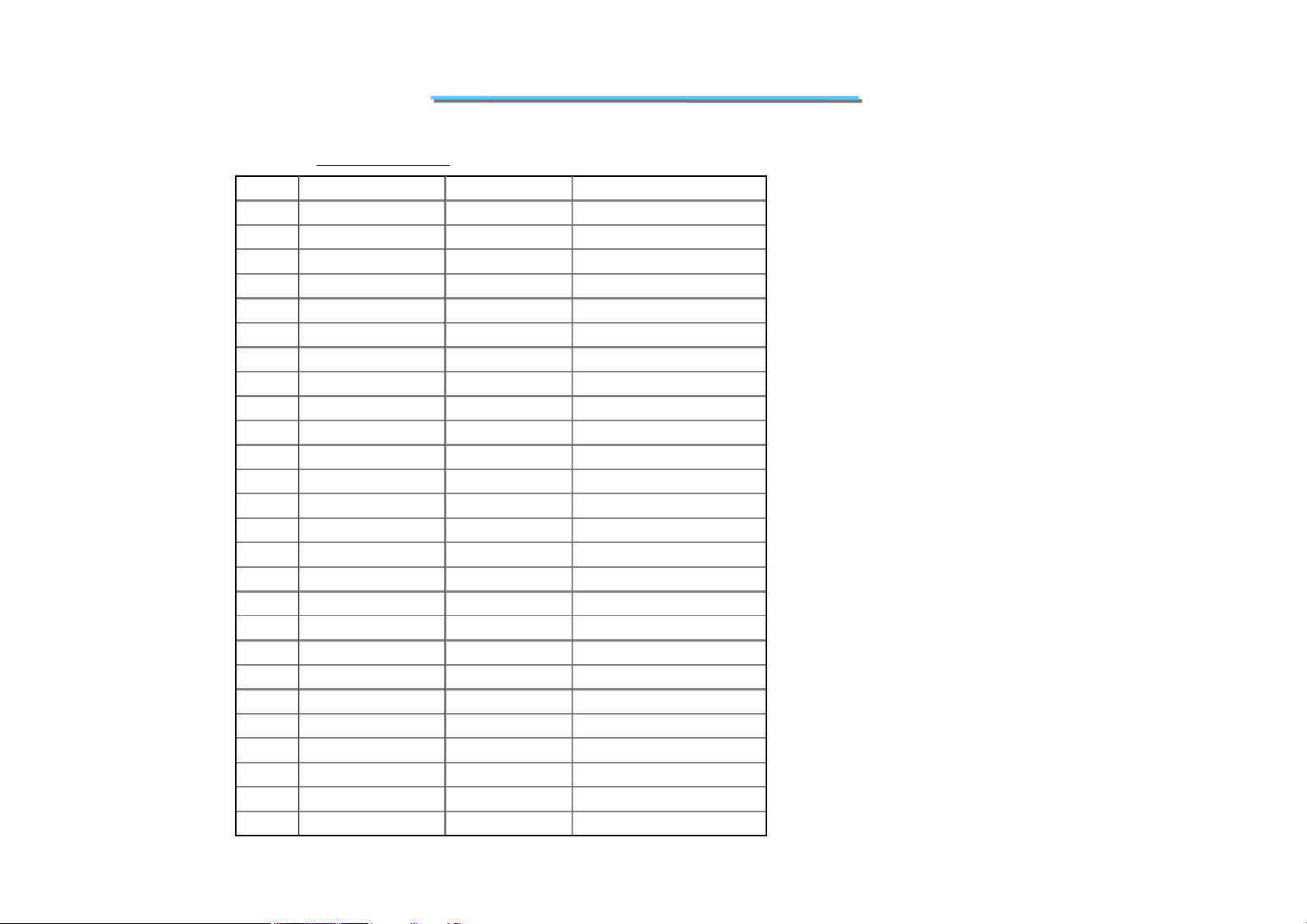
• Parallel Port
@ Configurable as logical ports LPT1,LPT2 or LPT3
Figure 1.7 USB Port
@ EPP rev 1.7 & 1.9 compatible
@ ECP(IEEE 1284) compatible
@ Industry standard 25 Pins connector
Figure 1.8 PARALLEL PORT CONNECTOR
17
8170 N/B MAINTENANCE
Table 1.8 PARALLEL Port
PIN SIGNAL NAME DIRECTION DESCRIPTION
1 STROBE# O Data Strobe
2 PD0 I/O PP Data bit 0
3 PD1 I/O PP Data bit 1
4 PD2 I/O PP Data bit 2
5 PD3 I/O PP Data bit 3
6 PD4 I/O PP Data bit 4
7 PD5 I/O PP Data bit 5
8 PD6 I/O PP Data bit 6
9 PD7 I/O PP Data bit 7
10 -ACK I Printer Acknowledge
11 BUSY I Printer Busy
12 PE I Paper Out
13 SLCT I Print Select Acknowledge
14 -AUTOFDXT O Auto Line Feed
15 -ERROR I Printer Error
16 -INIT O Reset Printer
17 SLCTIN# I Select In
18 GND - Ground
19 GND - Ground
20 GND - Ground
21 GND - Ground
22 GND - Ground
23 GND - Ground
24 GND Ground
25 GND - Ground
Case GND - Ground
18

8170 N/B MAINTENANCE
1.2.2.5 PC CARD SLOT
One Type II/I slot supporting the 1997 PC Card standard, and including full R2(16-bit) and 32-bit Card
bus Data transfer
TI PCI4410(PCMXCIA Controller)& TI TPS2211(Power Switch)
1.2.2.6 GRAPHICAL SUBBSYSTEM
ATI Mobility M6 graphical controller embedded 8M DDR SDRAM
1.2.2.7 DISPLAY
Internal LCD Display is 14.1” TFT ISP XGA color
External Video refresh rate of up to 100HZ support
---Vertical refresh frequencies to meet VESA requirements
---Simultaneous video in specified video modes-switchable with hot key
1.2.2.8 READ ONLY MEMORY(BIOS FLASH)
Fully compatible with industry standard software including windows 2000 & Windows XP
Fully support APM V1.2 and latest ACPI specification
4Mb Flash BIOS
Inside BIOS core
1.2.2.9 POWER MANAGEMENT FEATURES
Local standby mode(individual device such as HDD, graphics controller,LCD etc..)
19

8170 N/B MAINTENANCE
CPU Idle mode(including ACPI modes C1 and C2)
Suspend mode(including S1 and S3 ACPI modes)
Fully APM V1.2 compliant
Fully ACPI V1.1 compliant
Hibernate for Windows 2000 and windows XP
Thermal management
Fully US EPA Energy start compliant
1.2.2.10 KEYBOARD CONTROLLER
Hitachi H8-3437S
1.2.2.11 SUPER I/O
Ns PC87393F LPC interface Ultra I/O
1.2.2.12 LEDS INDICATOR
CDROM & HDD & NUM & CAP & SCROLL & EMIAL
1.2.2.13 BUTTONS
EMAIL BIN & FIVE PIECE EASY START RTN
20
8170 N/B MAINTENANCE
1.2.2.14 MODEM
Table 1.9 MODEM DAUGHTER BOARD CONNECTOR
PIN SIGNAL NAME PIN SIGNAL NAME
1 MONO_OUT 2 NC
3 GND 4 MODEM_SPK
5NC6NC
7NC8GND
9NC10+5V
11 NC 12 NC
13 NC 14 NC
15 GND 16 Pull Up to +3V
17 +3V 18 +5V
19 GND 20 GND
21 +3V 22 ACSYNC
23 ACSDOUT 24 MSDIN
25 -ACRST 26 MSDIN
27 GND 28 GND
29 GND 30 ACBITCLK
21
8170 N/B MAINTENANCE
1.3 Electrical Characteristic
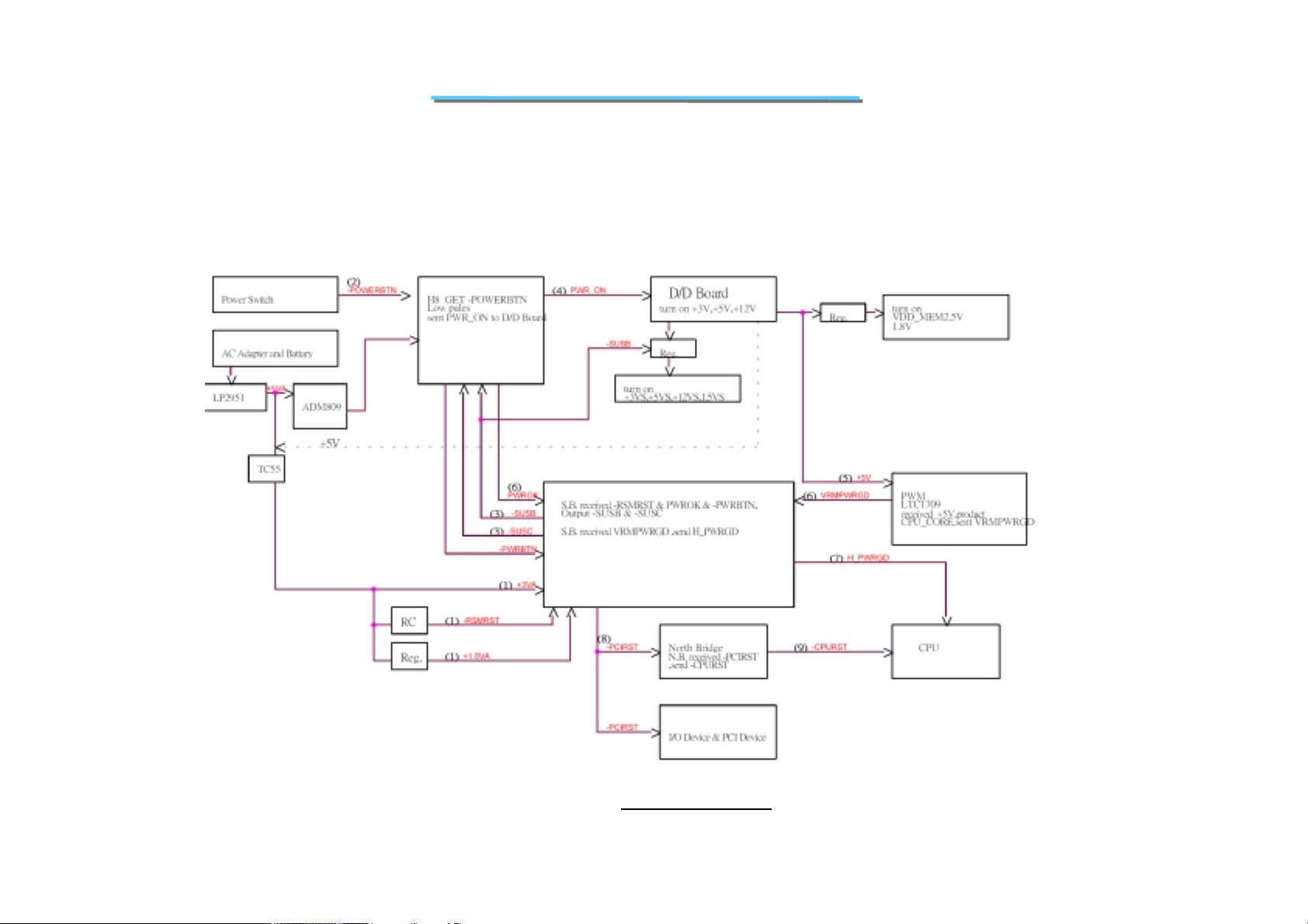
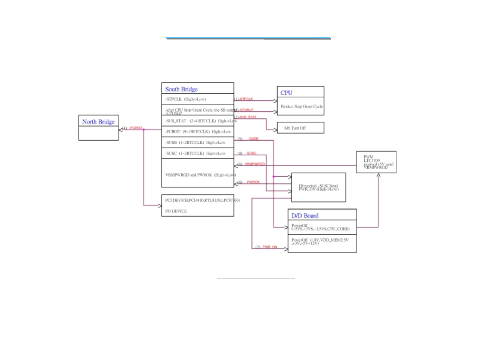
1.3.1 Power On Sequence
Figure 1.9 Power on Sequence
22
8170 N/B MAINTENANCE
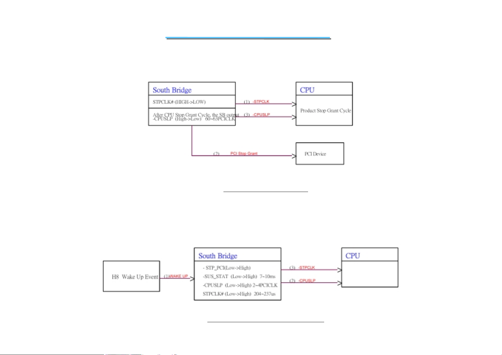
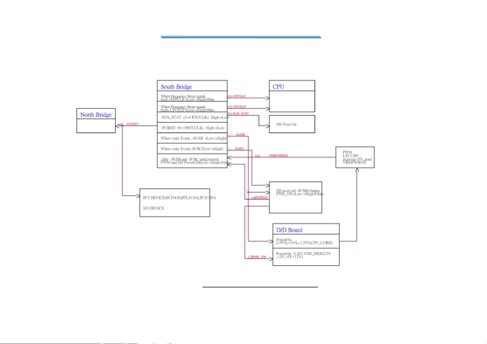
1.3.2 Power On Suspend Seque nce
Figure 1.10 Power on Suspend Sequence
1.3.3 Resume from Power Susp end Sequence
Figure 1.11 Resume from Power Suspend Sequence
23
8170 N/B MAINTENANCE
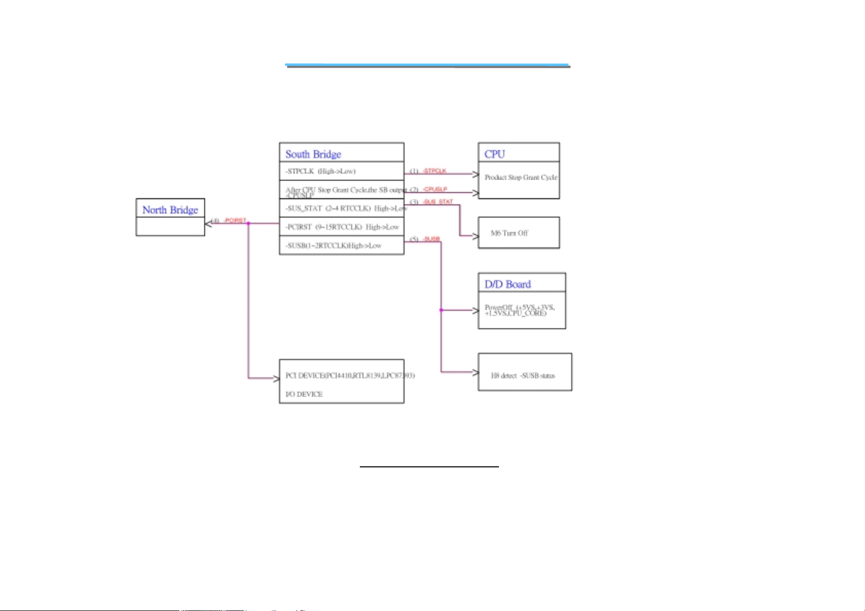
1.3.4 Suspend to RAM Sequenc e
Figure 1.12 Suspend to RAM sequence
24
8170 N/B MAINTENANCE
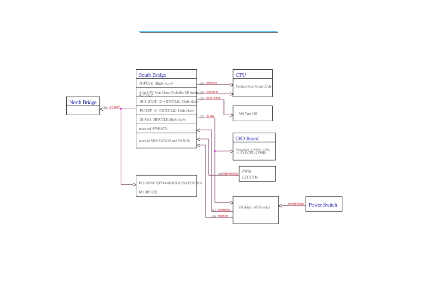
1.3.5 Resume from Suspend to RAM Seque nce
Figure 1.13 Resume from Suspend to RAM Sequence
25
8170 N/B MAINTENANCE
1.3.6 Suspend to Disk Sequence
Figure 1.14 Suspend to Disk Sequence
26
8170 N/B MAINTENANCE
1.3.7 Resume from Suspend to Disk Sequenc e
Figure 1.15 Resume from Suspend to Disk Sequence
27
8170 N/B MAINTENANCE
6
K
E
1.3.8 ICH2 GPI/O Pin Define
Pin Name Signal Name Power Type During
PCIRST#
GPIO0 PULL-UP + 3. 3VS I PC/ PCI DEVI CE DRI VEN
GPIO1 PULL-UP + 3. 3VS I PC/ PCI DEVI CE DRI VEN
GP IO 2 P ULL -U P + 3. 3VS X X X X X X X
GPIO3 PULL-UP +3.3VS I HIGH-Z HIGH-Z HIGH-Z
GPIO4 PULL-UP +3.3VS I HIGH-Z HIGH-Z HIGH-Z
GPIO6 PULL-UP + 3. 3VS I MA IN I/ O
GP IO 7 P ULL -U P + 3. 3VS I
GP IO 8
GPIO11 PULL-UP +3.3VA I HIGH-Z HIGH-Z DEFINED DEFINED DEFINED
GPIO12 -EXTSMI +3.3VA I DOS MODE -SMI
GPIO13 PULL-UP +3.3VA I
GP IO 1
GPIO17 PULL-UP +3.3VS O HIGH-Z HI HI OFF OFF
GPIO18 PULL-UP +3.3VS O HI DEFINED OFF OFF
GPIO19 -ENABKL_MAS
GP IO 20-CDROM_PW RON +3.3VS O HI HI DEFINED OFF OFF Contro l CDROM Power on
GPIO21 -HDD_PW RON +3.3VS O HI HI DEFINED OFF OFF Con tro l HDD Po wer o n
GPIO22 DRAMENA +3.3VS O HIGH-Z HIGH-Z DEFINED OFF OFF DRAM Data s elect
GPIO23 PULL-UP +3.3VS OD LOW LOW DEFINED OFF OFF
GPIO24 -1394WR +3.3VA O HIGH-Z HI DEFINED DEFINED DEFINED 1394EEPROM R/W
GPIO25 -PCIRST_ MSK +3.3VA O HIGH-Z HI DEFINED DEFINED DEFINED MASK PCIRST
GPIO27 -GATE1394 +3.3VA O HIGH-Z HI DEFINED DEFINED DEFINED RST CARD BOARD
GPIO28 SPK_OFF +3.3VA O HIGH-Z HI DEFINED DEFINED DEFINED OFF SPEAKER
-SCI
TP +3.3VS O HIGH-Z HI HI OFF OFF
+3.3VA I ACPIMODE-SCI
+3.3VS O HI HI DEFINED OFF OFF M A SK ENA BL
Imm ediately After
PCIRST#
S1 S3 S4/S5 Description
28
8170 N/B MAINTENANCE
1.3.9 Power Consumption Of Suspend Mode
Suspend To RAM<TBD
Suspend To Disk/Soft-Off/Mechanical Off<TBD
1.3.10 Clock Harmonic List
Clock Harmonic
12.288 14.318 16 24 24.576 25 27 32.758 33 48 65 66 100 133
12.288 14.318 16 24 24.576 25 27 32.758 33 48 65 66 100 133
1
24.576 28.636 32 48 49.152 50 54 65.516 66 96 130 132 200 266
2
36.864 42.954 48 72 73.728 75 81 98.274 99 144 195 198 300 399
3
49.152 57.272 64 96 98.304 100 108 131.032 132 192 260 264 400 532
4
61.44 71.59 80 120 122.88 125 135 163.79 165 240 325 330 500 665
5
73.728 85.908 96 144 147.456 150 162 196.548 198 288 390 396 600 798
6
86.016 100.226 112 168 172.032 175 189 229.306 231 336 455 462 700 931
7
98.304 114.544 128 192 196.608 200 216 262.064 264 384 520 528 800 1064
8
110.592 128.862 144 216 221.184 225 243 294.822 297 432 585 594 900 1197
9
122.88 143.18 160 240 245.76 250 270 327.58 330 480 650 660 1000 1330
10
135.168 157.498 176 264 270.336 275 297 360.338 363 528 715 726 1100 1463
11
147.456 171.816 192 288 294.912 300 324 393.096 396 576 780 792 1200 1596
12
159.744 186.134 208 312 319.488 325 351 425.854 429 624 845 858 1300 1729
13
172.032 200.452 224 336 344.064 350 378 458.612 462 672 910 924 1400 1862
14
184.32 214.77 240 360 368.64 375 405 491.37 495 720 975 990 1500 1995
15
196.608 229.088 256 384 393.216 400 432 524.128 528 768 1040 1056 1600 2128
16
208.896 243.406 272 408 417.792 425 459 556.886 561 816 1105 1122 1700 2261
17
221.184 257.724 288 432 442.368 450 486 589.644 594 864 1170 1188 1800 2394
18
233.472 272.042 304 456 466.944 475 513 622.402 627 912 1235 1254 1900 2527
19
245.76 286.36 320 480 491.52 500 540 655.16 660 960 1300 1320 2000 2660
20
258.048 300.678 336 504 516.096 525 567 687.918 693 1008 1365 1386 2100 2793
21
270.336 314.996 352 528 540.672 550 594 720.676 726 1056 1430 1452 2200 2926
22
282.624 329.314 368 552 565.248 575 621 753.434 759 1104 1495 1518 2300 3059
23
294.912 343.632 384 576 589.824 600 648 786.192 792 1152 1560 1584 2400 3192
24
307.2 357.95 400 600 614.4 625 675 818.95 825 1200 1625 1650 2500 3325
25
Unit: M
29
 Loading...