

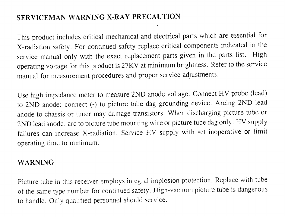
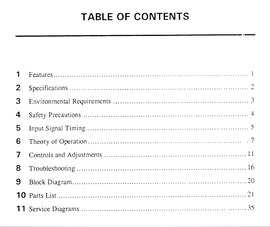
Mitac 1766PD Service Manual

S
ervice Manual
Monitoare
MITAC.
MITAC.
MITAC.
MITAC.
General Partner
T
echnical worl
d
®
PC
1766PD.
L-1766PD.
M-1766PD.
M/L-1766PD.
1. FEATURES
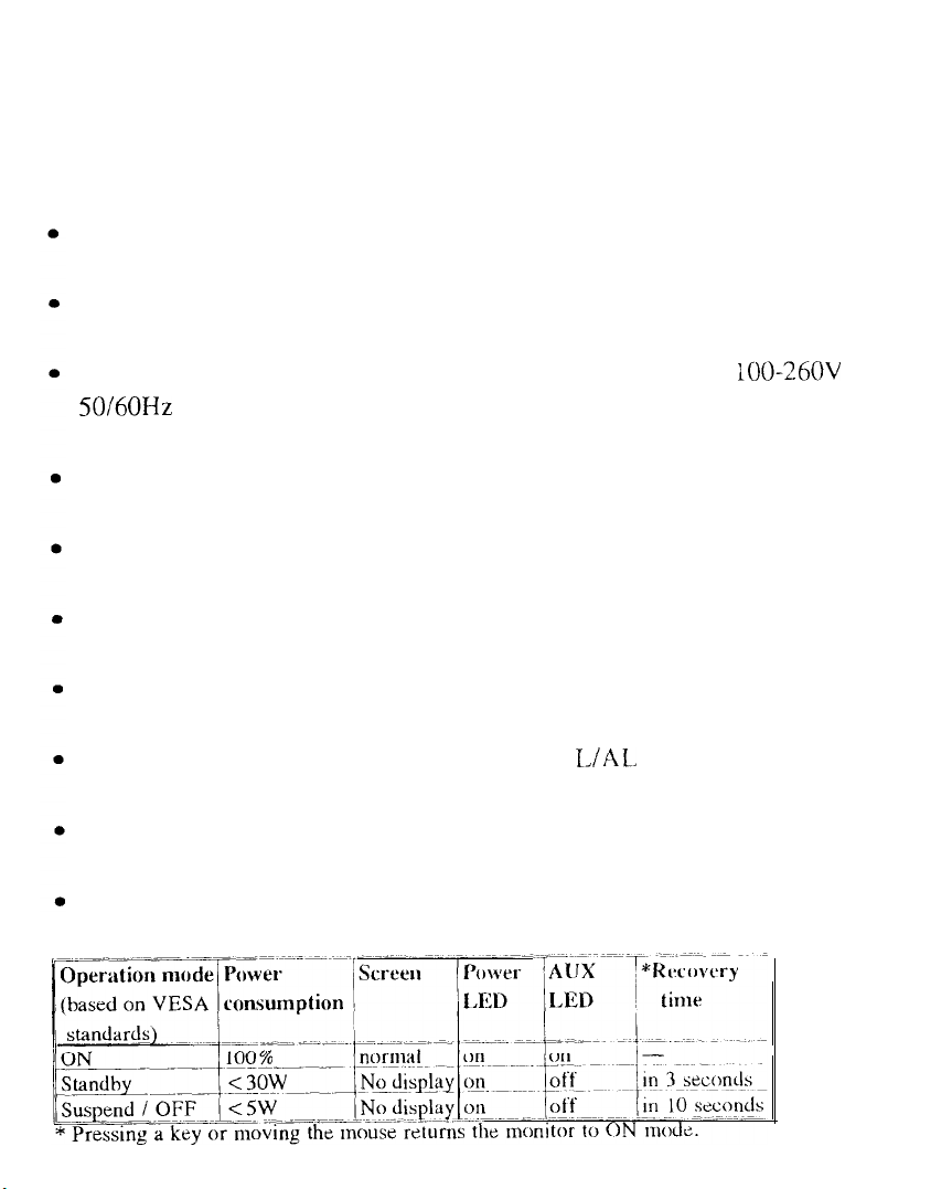
This monitor specifically provides the following features:
Microprocessor-based design with digital control
Non-volatile memory for 10 factory preset and 10 user-defined timing modes
Built-in switching regulator power circuit, can be used with
50/60Hz universal power supply
Manual degaussing
Display rotation
True color adjustment (red-green-blue)
Full screen
Low electro-magnetic radiation emission (for
OSD (on-screen display) control function
Green machine (power saving):
L/AL,
model)
100-260V
AC,
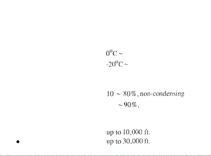
3. ENVIRONMENTAL REQUIREMENTS
Temperature
O°C -
l ENCLOSED CABINET:
40°C (operating)
Humidity
. OPERATING:
. STORAGE:
Altitude
. OPERATING:
.
STORAGE:
-2OOC -
10 - 80%)
60°C (storage)
nOJl-COlldeJlSiJl~
10 - 90%, non-condensing
up to 10,000
up to
30,000 ft.
l-t.

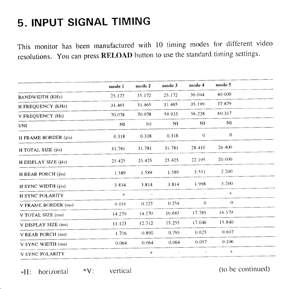
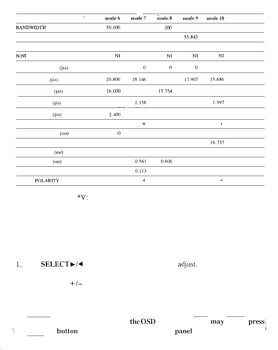
BANDWlDTH
H FREQUENCY (KHz)
V FREQUENCY (Hz)
N/N1
(KHz)
50.000 44.908
48.077 35.528 48.363 55.843
72.188 86.972 60.004 69.979
NI
65
.ocu
I
74.161 11.016
NI NI
63.750
59.747
NI
H FRAME BORDER
H TOTAL SIZE (Its)
H DISPLAY SIZE
H REAR PORCH
H
SYNC WIDTH
H SYNC POLARITY
V FRAME BORDER
V TOTAL SIZE (ms)
V DISPLAY SIZE
V REAR PORCH
V SYNC WIDTH (ms)
V SYNC
POLARKY
*H: horizontal
(Its)
(111;)
(cts)
(11s)
(ms)
(ins)
(ms)
*V:
20.x00
lh.Ocx)
13.x53
12.480 IO.808
vertical
0
1.280
-__
2.400 3.919 2.092 2.373
+ +
0
0.478 0.563 0.600 0.537
0.125 0.113
+
0
28.146 20.677 17.907
22.802
1.1%
0 0 0
Il.498
t
0 0
15.754
2.462
16.666 14.290
IS.880
0.124
13.808
I.294
13.663
0.072
0
IS.686
Il.620
I.997
1.489
t
0
16.737
16.062
0.596
0.047
i
(continued)
This monitor also provides 10 blank storage areas for the control settings of each timing
mode. If you are not satisfied with the standard settings for a certain mode, you can
define your own settings following this procedure:
1.
Use
SELECT,/4
2.
Use ADJUST + I- to ad-just the value of that option.
3.
Press STATUS to save the settings.
(If you change the video mode while
\
the STATUS button before you can use the control
to select the option you want to
the OS11
is activated, you
acl_just.
panel
may
buttons.
have to
press)
I
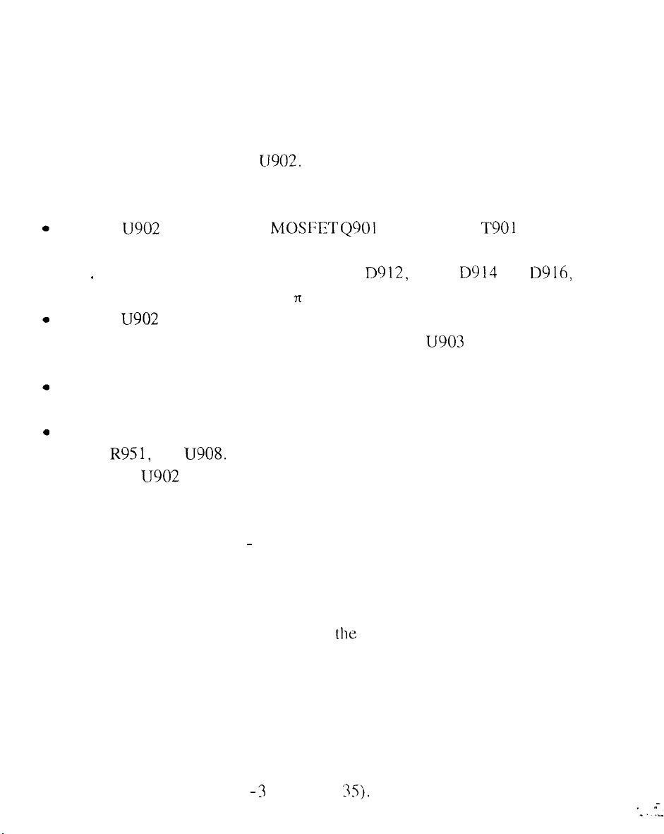
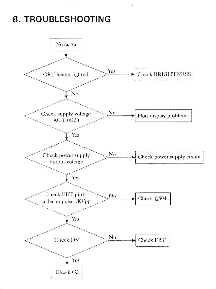
6. THEORY OF OPERATION
Switch Mode Power Supply
The current mode control IC is
<J902.
To avoid the screen being interfered, its circuit
applies SYNC trigger.
Pin 6 of
U902
directly drives
JviIOSFET Q901
and oscillates
T901
transformer,
so that energy will be transferred from the primary voltage to the secondary voltage . The secondary voltage is rectified by D912, D913,
D914
and
D916,
tain output voltage by way of the n filter circuit.
Pin 3 of
T901 via R919. Via pin 2 of 17902, the feedback of
U902
offers over current protection, which detects the source current of
U903
rectifies the output
voltage from pin 3 of R9 19.
TH801 is a positive temperature coefficient resistance. It performs degaussing
function when the power is on.
The power saving circuit consists of C927, Q902, Q903, Q908, R928, R929,
R942,
on pin 1 of
R951,
and
U908.
If the vertical SYNC signal doesn’t appear, the voltage
U902
will shut down, and the SMPS (Switch Mode Power Supply)
will be OFF.
See figure SD640012120021 - 1 of 3 (page 35).
to ob-
Input Circuit
From the SYNC signal of U 101, we know
the
shaping and polarity status. We also get
positive horizontal SYNC output from pin 6, and positive vertical SYNC output from
pin 8.
In order to make sure that the horizontal SYNC output and vertical SYNC output have
the same pulse width, we use U 102.
See figure SD640012120021
- 3
of 3 (page
35).

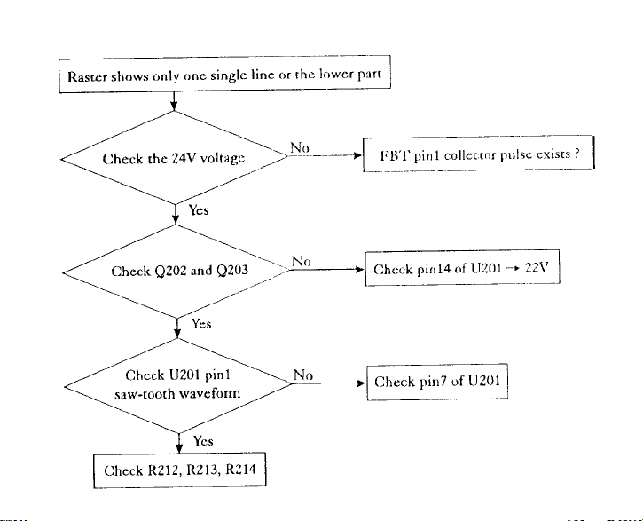
Horizontal Driver Circuit
The output point of the horizontal driver pulse is pin 8 of
U305.
T.501 increases the horizontal driver pulse current to drive Q.504.
B+ parabolic wave flows into
C.506, C507, C508
are controlled by
L401
to modify a
Q505
and
pinchushion.
(2506
to get the horizontal linearity .
L501
is a variable horizontal linearity coil.
See figure SD640012120021 - 3 of 3 (page 35).
High Voltage Driver Circuit
This is a diode modulation circuit. The horizontal deflection and the high voltage are integrated together.
The tunning capacitors C5 12 and C5 14, which are controlled by
RI>501
,
used to keep the high voltage.
FBT generates 24KV,
See figure SD640012120021 - 3 of 3 (page
-17OV
and the feedback signal.
35)
are
Step-down B + Circuit
l
U801
is adopted to be a monostable circuit, triggered by pin 4 of FBT. The
square wave comes out from pin 3 of
l
C.517,
D802,
L802,
and QS 10 generate the step-down
U801.
See figure SD640012120021 - 3 of 3 (page 35).
Double Focus Circuit
l
U402
generates the vertical parabolic wave.
l
L603, C611
l The
hrizontal
and C613 generate the horizontal parabolic wave.
and vertical parabolic waves are integrated by
to pin 11 of FBT.
See figure SD640012
12002
1 - 3 of 3 (page 35).
R+.
T601
and then sent
OSD Microprocessor Circuit
The
84C882
For
84C882,
The
The vertical SYNC goes through
is a
g-bit
microprossor. The PCF8582 is the EPROM.
FB/GO/BO/RO signal comes from pin
pirt
5.
1,
2,
3,
?
4.
The horizontal SYNC goes through pin 6 and pin 11.
PWM signal comes from pin 9, 24, 25, 26, 27,
The
28, 29,
37,
and 38.
Pin 33 provides the RESET function.
frequency detection signals come
The
When pin 19 is under the “active low”
from
pin 13,
14,
mode, it provides the MUTE function.
15,
16,
17, 18.
When pin 20 is under the “active high” mode, it provides the DEGAUSSING
function.
See figure SD6400 12 12002
Video Amplifier Circuit
LM1207 is a
l The R/G/B signal goes through pin 4, 6, 9.
l The R/G/B signal comes from pin 26, 20, 17.
l The R/G/B gain is controlled by pin 28, 18,
l The R/G/B bias is controlled by pin 27, 19, 16.
l The negative clamp pulse comes from pin 14.
l The contrast DC level is controlled by pin 12.
l The R/G/B video output cascade circuit consists of
R711,
l The SEPP (Single End Push Pull) circuit consists of
85MHz
R7 12,
pre-amplifier IC.
R705,
R706, and
1 -
2 of 3 (page
C704.
35)
_
15.
Q701,
Q507
used to increase the video bandwidth for the K/G/B video output.
See figure SD640012 120023 (page 35).
Q702,
and
Q504,
D701, L701,
which is

6.
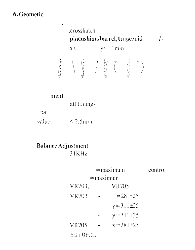
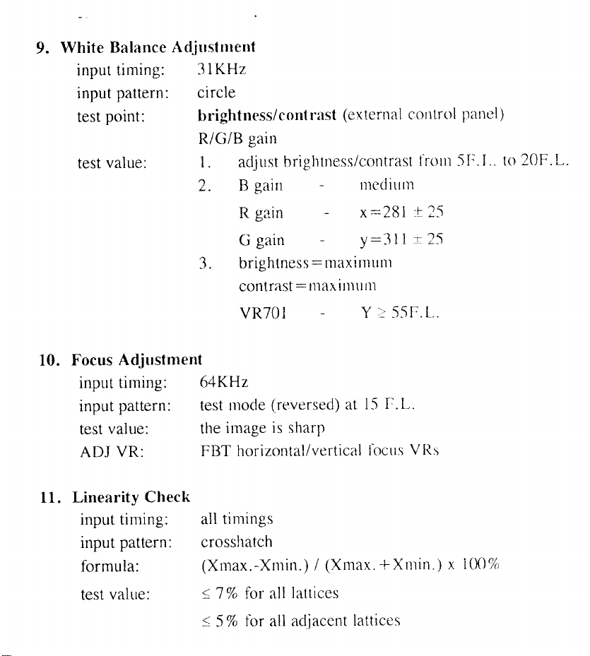
Geornetic Adjustment
input timing:
_
input pattern:
test point:
ail
timings
_crosshatch
pis~cushioll/h~~~,I-cl,
t
rapczoid
and + I- buttons
test value:
7. Tile Adjust
input timing:
input
test
rnent
pal
tern: crosshatch
value:
ADJ VK: rotate VR
8. Dark
Balarlcc
Adjustrl~erlt
input timing:
input pattern: raster
test point:
xl:
0.2111111, y’ 0. 1Jntn
dl
1illiiIlgS
I
2.5nllll
31KHz
brightness =maximum (external
conk01
panel)
contrast =maxinliun (external control panel)
VR70.1,
VR704,
VI1705
= maximum
test value:
VR703
VR704
VR7OS
YI I .OF.L.
-
-
-
x
=28 1225
y=311rm
y=3l l-t25
x=281k25
 Loading...