MCC MURX0510, MURX0550, MURX0560, MURX0540, MURX0530 Datasheet
...
M C C
omponents 21201 Itasca Street Chatsworth
! "# $% ! "#
Features
•For Surface Mount Application
•Low Leakage
•Low Forward Voltage Drop
•Extremely Low Thermal Resistance
•Super Fast Recovery Time For High Efficiency
Maximum Ratings
•Operating Temperature: -40 to +150
•Storage Temperature: -40 to +150
•Maximum Thermal Resistance: 200 /W Junction to Ambient
|
|
Maximum |
|
Maximum |
|
|
Recurrent |
Maximum |
DC |
MCC |
Device |
Peak Reverse |
RMS |
Blocking |
Part Number |
Marking |
Voltage |
Voltage |
Voltage |
MURX0510 |
U1 |
100V |
70V |
100V |
|
|
|
|
|
MURX0520 |
U2 |
200V |
140V |
200V |
|
|
|
|
|
MURX0530 |
U3 |
300V |
210V |
300V |
|
|
|
|
|
MURX0540 |
U4 |
400V |
280V |
400V |
|
|
|
|
|
MURX0550 |
U5 |
500V |
350V |
500V |
|
|
|
|
|
MURX0560 |
U6 |
600V |
420V |
600V |
|
|
|
|
|
Electrical Characteristics @ 25 Unless Otherwise Specified
|
Average Forward |
IF(AV) |
0.5 A |
TL = 115 |
|
Current |
|||
|
|
|
|
|
|
|
|
|
|
|
Peak Forward Surge |
IFSM |
8.0A |
8.3ms, half sine |
|
Current |
|||
|
|
|
|
|
|
|
|
|
|
|
Maximum |
|
|
IFM =0.5A; |
|
Instantaneous |
VF |
1.35V |
|
|
TA = 25 |
|||
|
Forward Voltage |
|
|
|
|
|
|
|
|
|
|
|
|
|
|
Maximum DC |
|
|
|
|
Reverse Current At |
IR |
5.0 A |
TA = 25 |
|
Rated DC Blocking |
|||
|
|
|
|
|
|
Voltage |
|
|
|
|
|
|
|
|
|
Maximum Reverse |
Trr |
75ns |
IF=0.5A, IR=1.0A, |
|
Recovery Time |
Irr=0.25A |
||
|
|
|
||
|
Typical Junction |
CJ |
10pF |
Measured at |
|
Capacitance |
1.0MHz, VR=4.0V |
||
|
|
|
||
|
*Pulse Test: Pulse Width |
300 sec, Duty Cycle 2% |
||
MURX0510
THRU
MURX0560
0.5 Amp Super Fast
Recovery Rectifier
100 to 600 Volts
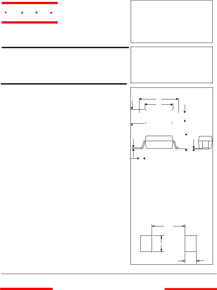
SOD-123
A
B
C |
|
|
|
|
|
|
|
|
|
|
|
|
|
|
|
|
|
|
|
|
|
|
|
|
|
|
|
||
|
|
|
|
|
|
|
|
|
|
E |
|
|||
|
|
|
|
|
|
|
|
|
|
|
|
|
|
|
|
|
|
|
|
|
|
|
|
|
|
|
|
|
|
|
|
|
|
|
|
|
|
|
|
|
|
|
|
|
|
|
|
|
|
|
|
|
|
|
|
|
|
|
|
|
|
|
|
|
|
|
|
|
|
|
|
|
|
|
|
|
|
|
|
|
|
|
|
|
|
|
|
|
|
|
|
|
|
|
|
|
|
|
|
|
|
|
|
|
H
D
|
|
|
G |
|
|
|
|
|
J |
|
|
|
|
|
|
|
|
|
|||
|
|
|
|
|
|
|
|
|||
|
|
|
|
|
|
|
|
|
|
|
|
|
|
|
DIMENSIONS |
|
|
|
|
||
DIM |
INCHES |
MM |
|
|
|
NOTE |
||||
|
|
MIN |
|
MAX |
MIN |
|
MAX |
|
|
|
|
|
|
|
|
|
|
|
|
|
|
A |
.140 |
|
.152 |
3.55 |
|
3.85 |
|
|
|
|
B |
.100 |
|
.112 |
2.55 |
|
2.85 |
|
|
|
|
C |
.055 |
|
.071 |
1.40 |
|
1.80 |
|
|
|
|
|
|
|
|
|
|
|
|
|
|
|
D |
----- |
|
.053 |
----- |
|
1.35 |
|
|
|
|
E |
.012 |
|
.031 |
0.30 |
|
.78 |
|
|
|
|
G |
.006 |
|
----- |
0.15 |
|
----- |
|
|
|
|
|
|
|
|
|
|
|
|
|
|
|
H |
----- |
|
.01 |
----- |
|
.25 |
|
|
|
|
J |
----- |
|
.006 |
----- |
|
.15 |
|
|
|
|
|
|
|
|
|
|
|
|
|
|
|
SUGGESTED SOLDER
PAD LAYOUT
0.093”
0.048”
0.036”
www.mccsemi.com
 Loading...