

Page 1
Service
-
+
-+
-
+
+
Manual
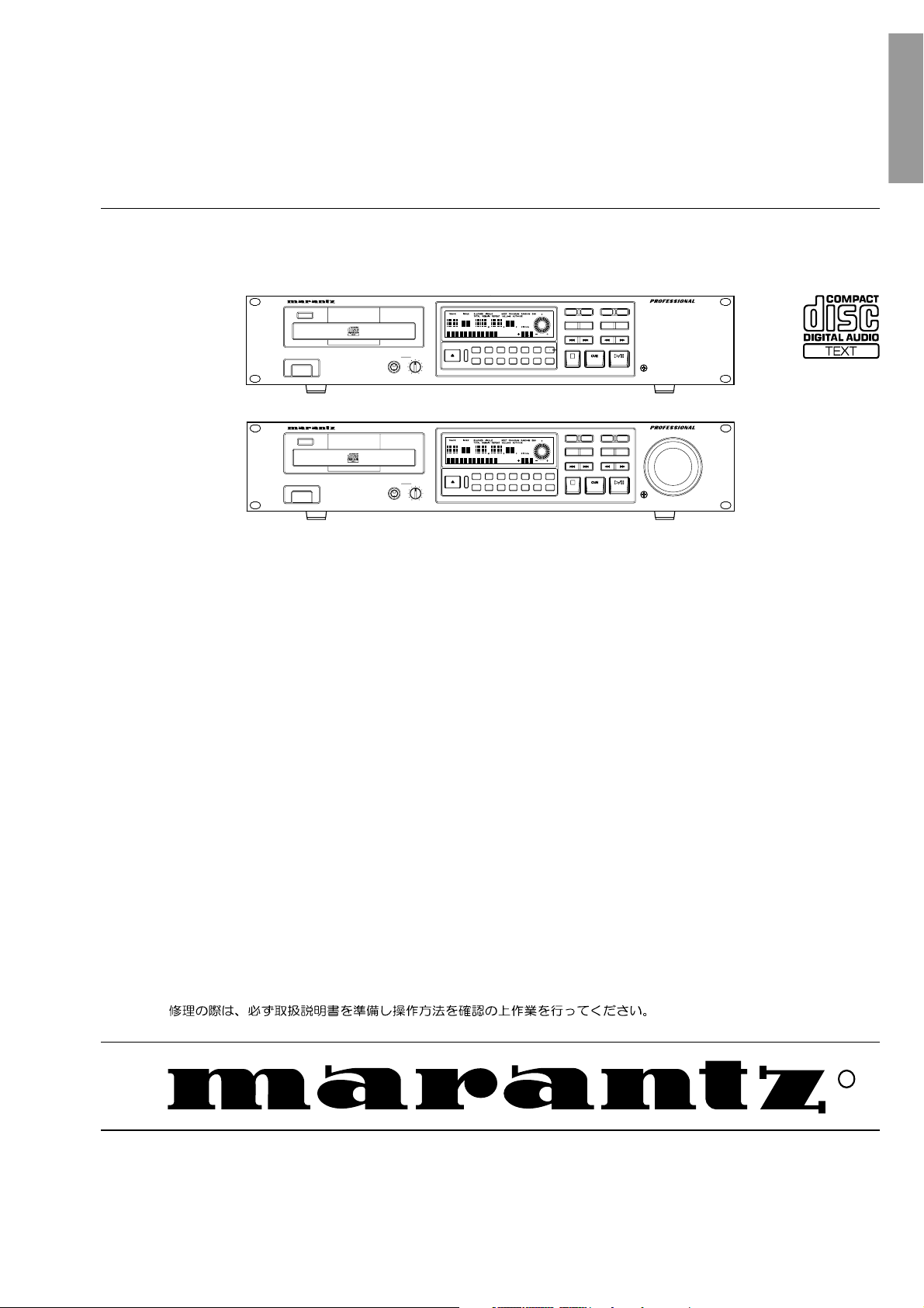
PMD330 /N1M, /U1B, /F1B
PMD331 /N1M, /U1B, /F1B
PMD340 /N1M, /U1B, /F1M
PMD330/331/340
CD Player
PMD330
CD PLAYER
IR
TIME
21
POWER
LEVELHEADPHONE
MAXMIN
3
TEXT
8
6
7
MODE
5
4
PROG
PRESET
9
0
A-B PITCH
END
INDEX PITCH
CLEAREXIT
ON/OFF
ENTER
CONTRAST
PMD331 / 340
CD PLAYER
IR
216TIME
POWER
LEVELHEADPHONE
MAXMIN
3
TEXT
8
7
MODE
-
4
5
PROG
9
PRESET
0
A-B PITCH
END
INDEX PITCH BEND
--+
CLEAREXIT
ON/OFF
+
ENTER
CONTRAST PITCH / SEARCH
TABLE OF CONTENTS
SECTION PAGE
1. TECHNICAL SPECIFICATIONS ................................................................................................................. 1
2. SERVICE HINTS ....................................................................................................................................... 2
3. SERVICE TOOLS ..................................................................................................................................... 2
4. ADJUSTMENT AND SERVICE MODE .................................................................................................. 3
5. MICROPROCESSOR AND IC DATA..................................................................................................... 5
6. WIRING DIAGRAM ................................................................................................................................. 13
7. BLOCK DIAGRAM .................................................................................................................................. 15
8. SCHEMATIC DIAGRAM......................................................................................................................... 17
9. PARTS LOCATIONS .............................................................................................................................. 24
10. EXPLODED VIEW AND MECHANISM PARTS LIST......................................................................... 28
11. TECHNICAL DESCRIPTION ..................................................................................................................... 31
12. ELECTRICAL PARTS LIST ................................................................................................................... 33
Please use this service manual with referring to the user guide ( D.F.U. ) without fail.
PMD330 / 331 / 340
R
371K855010 MIT
3120 785 22250
First Issue 1999.12
Page 2
MARANTZ DESIGN AND SERVICE
MARANTZ AMERICA, INC.
WILDASH AUDIO SYSTEMS NZ
Using superior design and selected high grade components, MARANTZ company has created the ultimate in stereo sound.
Only original MARANTZ parts can insure that your MARANTZ product will continue to perform to the specifications for which
it is famous.
Parts for your
MARANTZ equipment are generally available to our National Marantz Subsidiary or Agent.
ORDERING PARTS :
Parts can be ordered either by mail or by Fax.. In both cases, the correct part number has to be specified.
The following information must be supplied to eliminate delays in processing your order :
1. Complete address
2. Complete part numbers and quantities required
3. Description of parts
4. Model number for which part is required
5. Way of shipment
6. Signature : any order form or Fax. must be signed, otherwise such part order will be considered as null and void.
USA
MARANTZ AMERICA, INC
440 MEDINAH ROAD
ROSELLE, ILLINOIS 60172
USA
PHONE : 630 - 307 - 3100
FAX : 630 - 307 - 2687
AMERICAS
SUPERSCOPE TECHNOLOGIES, INC.
MARANTZ PROFESSIONAL PRODUCTS
2640 WHITE OAK CIRCLE, SUITE A
AURORA, ILLINOIS 60504 USA
PHONE : 630 - 820 - 4800
FAX : 630 - 820 - 8103
AUSTRALIA
JAMO AUSTRALIA PTY LTD
1 EXPO COURT, P.O. BOX 350
MT. WAVERLEY VIC 3149
AUSTRALIA
PHONE : +61 - 3 - 9543 - 1522
FAX : +61 - 3 - 9543 - 3677
NEW ZEALAND
WILDASH AUDIO SYSTEMS NZ
14 MALVERN ROAD MT ALBERT
AUCKLAND NEW ZEALAND
PHONE : +64 - 9 - 8451958
FAX : +64 - 9 - 8463554
EUROPE / TRADING
MARANTZ EUROPE B.V.
P.O.BOX 80002, BUILDING SFF2
5600 JB EINDHOVEN
THE NETHERLANDS
PHONE : +31 - 40 - 2732241
FAX : +31 - 40 - 2735578
AUSTRALIA
TECHNICAL AUDIO GROUP PTY, LTD
558 DARLING STREET,
BALMAIN, NSW 2041,
AUSTRALIA
PHONE : 61 - 2 - 9810 - 5300
FAX : 61 - 2 - 9810 - 5355
THAILAND
MRZ STANDARD CO.,LTD
746 - 754 MAHACHAI ROAD.,
WANGBURAPAPIROM, PHRANAKORN,
BANGKOK, 10200 THAILAND
PHONE : +66 - 2 - 222 9181
FAX : +66 - 2 - 224 6795
TAIWAN
PAI- YUING CO., LTD.
6 TH FL NO, 148 SUNG KIANG ROAD,
TAIPEI, 10429, TAIWAN R.O.C.
PHONE : +886 - 2 - 25221304
FAX : +886 - 2 - 25630415
BRAZIL
PHILIP DA AMAZONIA IND. ELET. ITDA
CENTRO DE INFORMACOES AO
CEP 04698-970
SAO PAULO, SP, BRAZIL
PHONE : 0800 - 123123
FAX : +55 11 534. 8988
(Discagem Direta Gratuita)
CANADA
LENBROOK INDUSTRIES LIMITED
633 GRANITE COURT,
PICKERING, ONTARIO L1W 3K1
CANADA
PHONE : 905 - 831 - 6333
FAX : 905 - 831 - 6936
SINGAPORE
WO KEE HONG (S) PTE LTD
WO KEE HONG CENTRE
NO.23, LORONG 8, TOA PAYOH
SINGAPORE 319257
PHONE : +65 2544555
FAX : +65 2502213
MALAYSIA
WO KEE HONG ELECTRONICS SDN. BHD.
SUITE 8.1, LEVEL 8, MENARA GENESIS,
NO. 33, JALAN SULTAN ISMAIL,
50250 KUALA LUMPUR, MALAYSIA
PHONE : +60 3 - 2457677
FAX : +60 3 - 2458180
JAPAN
Technical
MARANTZ JAPAN, INC.
35- 1, 7- CHOME, SAGAMIONO
SAGAMIHARA - SHI, KANAGAWA
JAPAN 228-8505
PHONE : +81 42 748 1013
FAX : +81 42 741 9190
KOREA
MK ENTERPRISES LTD.
ROOM 604/605, ELECTRO-OFFICETEL, 16-58,
3GA, HANGANG-RO, YONGSAN-KU, SEOUL
KOREA
PHONE : +822 - 3232 - 155
FAX : +822 - 3232 - 154
SHOCK, FIRE HAZARD SERVICE TEST :
CAUTION : After servicing this appliance and prior to returning to customer, measure the resistance between either primary AC
cord connector pins ( with unit NOT connected to AC mains and its Power switch ON ), and the face or Front Panel of product and
controls and chassis bottom.
Any resistance measurement less than 1 Megohms should cause unit to be repaired or corrected before AC power is applied, and
verified before it is return to the user/customer.
Ref. UL Standard No. 813.
In case of difficulties, do not hesitate to contact the Technical
Department at above mentioned address.
991207MIT
Page 3
1. TECHNICAL SPECIFICATIONS
PMD330 PMD331 / PMD340
General specifications
System Compact Disc - Digital Audio
Number of channels 2
Compatible discs CD-DA, CD-R, CD-RW (12 cm, 8 cm)
Audio characteristics
Channels 2 channels
Frequency characteristics 20 Hz to 20 kHz +/- 0.3 dB
Dynamic range ≥ 90 dB (1 kHz)
S/N ratio ≥ 100 dB (1 kHz)
Total harmonic distortion (THD) 0.005 % (1 kHz)
Wow and flutter Quartz precision
Error correction method Cross-interleave Read-Solomon code (CIRC)
Analog output Pin jack,unbalanced (RCA) 2.0V RMS Stereo
XLR jack,balanced (XLR) +16 dBu /600 Ω, @ 0 dB FS
(variable range) (-11 dBu to +21 dBu, variable)
Digital output Pin jack (SPDIF) 0.5 Vp-p/75 Ω
XLR jack (SPDIF) 3.5 Vp-p/110 Ω
optical connector -19 dBm
Search precision 1 frame
Pitch control Maximum: +/-12% in 0.1% steps
Pitch bend control +/- 8 %
Strat timing 20 ms
Remote control
Infrared remote control input IN (IR sensor)
RC5 remote control input/output RCA IN (INT/EXT switch)/OUT
Remote control input/output D-SUB 25-Pin female
Optical anning method
Laser AlGaAs semiconductor
Wavelength 780 nm
Signal system
Sampling frequency 44.1 kHz
Quantization 16-bit linear/channel
Power supply section
AC power supply /F : 100V, AC 50/60Hz, /N : 230V, AC 50Hz, /U : 120V, AC 60Hz
Power consumption 12 W 17 W
Cabinet, etc.
External dimensions (W x H x D) 483 x 100 x 325 mm (19 x 3-15/16 x 12- 13/16 inches)
Weight 4.8 kg (10.6 lbs) 4.9 kg (10.8 lbs)
Operating temperature range + 5°C to + 35°C
Operating humidity range 5% to 90% (without dew)
Due to our continuing efforts to improve our products, the specifications and appearance of this product are subject to change without
prior notice.
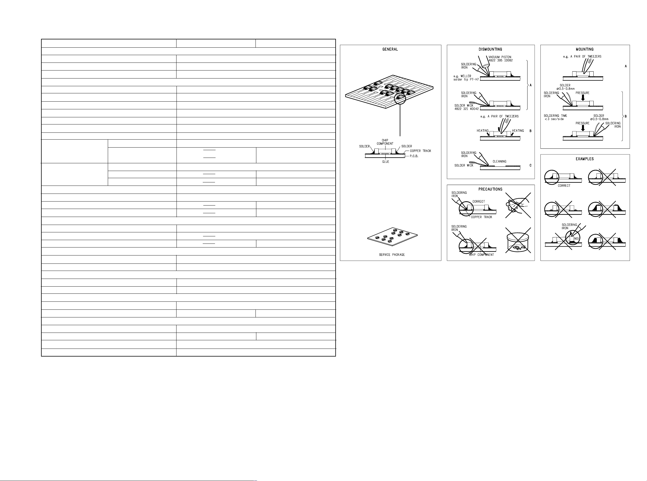
2. SERVICE HINTS
3. SERVICE TOOLS
Audio signals disc 4822 397 30184
Disc without errors (SBC444)+
Disc with DO errors, black spots and fingerprints (SBC444A) 4822 397 30245
Disc (65 min 1kHz) without no pause 4822 397 30155
Max. diameter disc (58.0 mm) 4822 397 60141
Torx screwdrivers
Set (straight) 4822 395 50145
Set (square) 4822 395 50132
13th order filter 4822 395 30204
1 2
Page 4
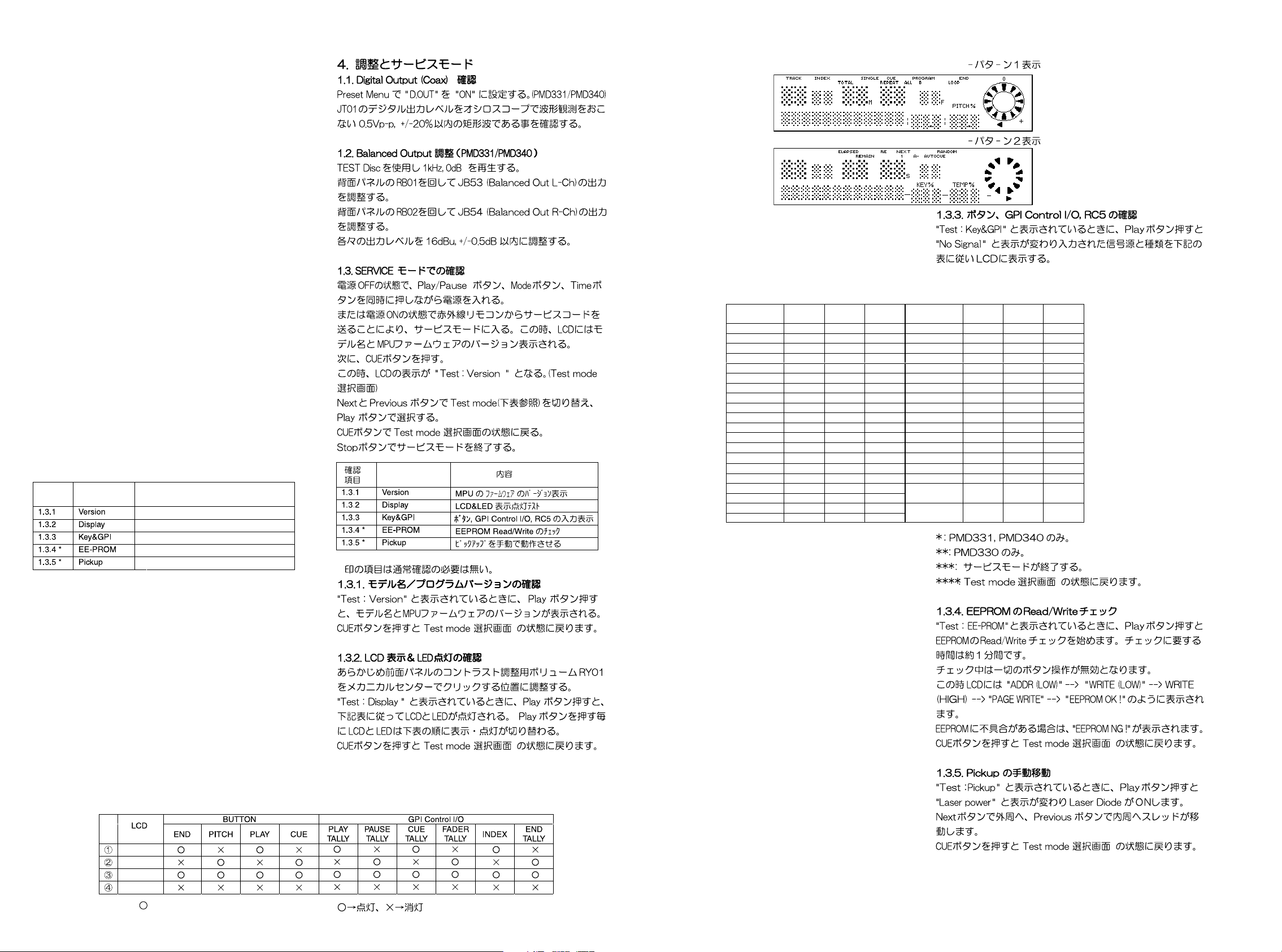
4. ADJUSTMENT AND SERVICE MODE
FUNCTION
SW
Input
GPI *
Input
RC5
Input
FUNCTION
SW
Input
GPI *
Input
RC5
Input
Open/Close 28 -- 29 Preset 33 -- 34
Time 29 -- 30 Index + 17 8 18
CD-Text 30 -- 31 Index - 18 9 19
Mode 31 -- 32 0 1 -- 2
Stop *** -- -- -- 1 2 -- 3
Cue **** -- -- -- 2 3 -- 4
Play/Pause 11 -- -- 3 4 -- 5
Play -- 1 12 4 5 -- 6
Cue + Play 13 4 -- 5 6 -- 7
Pause -- 2 13 6 7 -- 8
Next 15 10 16 7 8 -- 9
Previous 16 11 17 8 9 -- 10
FF 19 6 20 9 10 -- 11
REW
20 7 21
Pitch Bend +*26 -- 27
END 22 -- 23 Pitch Bend - *27 -- 28
A-B Repeat 21 -- 22
Pitch + 24 ** 13 25
Service
-- -- 35
Pitch - 25 ** 14 26
Program 32 -- 33
Fader
(Normal)
--
Fader
Input
--
Pitch On/Off
23 15 24
Fader
(Invert)
--
Fader
Input
--
1.1. Digital Output (Coaxial) Check
On the preset menu, set "D.OUT" to "ON".(PMD331/PMD340)
Do waveform observation with the oscilloscope, and confirm
the digital output level of JT01 to be 0.5Vp-p, square wave
within ±20% .
1.2. Balanced Output Adjustment (PMD331/PMD340)
1kHz, 0 dB are played back by using TEST disc.
Turn RB01 on the rear panel, and adjust the output of JB53
(Balanced Out L-CH).
Turn RB02 on the rear panel, and adjust the output of JB54
(Balanced Out R-CH).
Adjust each output level to 16 dBu, within ±0.5dB.
1.3. Service Mode
1) With power off, simultaneously press the PLAY/PAUSE,
MODE and TIME buttons, and at the same time, press the
power button. At this time the LCD shows the model name
and firmware version.
2) Next, press CUE button.
3) At this time the LCD shows " Test : Version ". (TEST MODE
select menu)
4) The NEXT and PREVIOUS buttons change the TEST
MODE(refer to the chart below). The PLAY button selects it.
5) Pressing the CUE button returns to the TEST MODE select
menu.
6) Press the STOP button to exit the service mode.
INDEX
It is not usually necessary to confirm.
*
TEST
MODE
MPU firmware version check
LCD&LED test
Confirmation of Buttons, GPI Control I/O and RC5
Check of EEPROM Read/Write
Manual moving of the pickup
1.3.1. Model name and firmware version check
When the LCD shows "Test : Version", press the PLAY button,
to see the model name and the MPU firmware version.
Pressing the CUE button returns to the TEST MODE select
menu.
1.3.2. LCD and LED test
1) Set the LCD panel contrast adjustment screw to mechanical center. (you will feel a click.)
2) When the LCD shows "Test : Display", press the PLAY button.
3) The LCD and LED lights as the chart below.
4) Each time the PLAY/PAUSE button is pressed the LCD and
5) Pressing the CUE button returns to the TEST MODE select
LED change as shown in the chart below.
menu.
PATTERN 1
PATTERN 2
All light up
None light up
CONTENTS
: Light X : Not Light
3 4
*
Test mode
PATTERN 1
PATTERN 2
1.3.3. Confirmation of Buttons, GPI Control I/O and RC5
1) When the LCD shows "Test : Key&GPI", press the PLAY
button.
2) The LCD shows "No Signal".
3) Press a button, GPI Control I/O and RC5 are input, and the
LCD changes as shown in the chart below.
: PMD331, PMD340 only. ** : PMD330 only.
*
: The service mode is exited.
***
: The TEST MODE select menu is returned.
****
1.3.4. Check of EEPROM Read/Write
1) When the LCD shows "Test : EE-PROM", press the PLAY
button.
2) Check of EEPROM Read/Write begins. The check takes
about 1 minute. During the check pressing any button has
no effect.
3) At this time the LCD shows as the following order.
"ADDR (LOW)"--->"WRITE (LOW)"--->"WRITE (HIGH)"
--->"PAGE WRITE"--->"EEPROM OK!"
4) If there is an error in the EEPROM, the LCD shows
"EEPROM NG!".
5) Pressing the CUE button returns to the TEST MODE select menu.
1.3.5. Manual moving of Pick up
1) When the LCD shows "Test : Pickup", press the PLAY button.
2) The LCD shows "Laser power". The laser diode turns on.
3) Press the NEXT button. The sled will move to the outside.
4) Press the PREVIOUS button. The sled will move to the inside.
5) Pressing the CUE button returns to the TEST MODE select
menu.
Page 5
Pin Name Function
CS
Chip Select
SCK Serial Data Clock
SI Serial Data Input
SO Serial Data Output
GND Ground
VCC Power Supply
WP
Write Protect
HOLD
Suspends Serial Input
NC No Connect
DC Don’t Connect
1
2
3
4
8
7
6
5
CS
SO
WP
GND
VCC
HOLD
SCK
SI
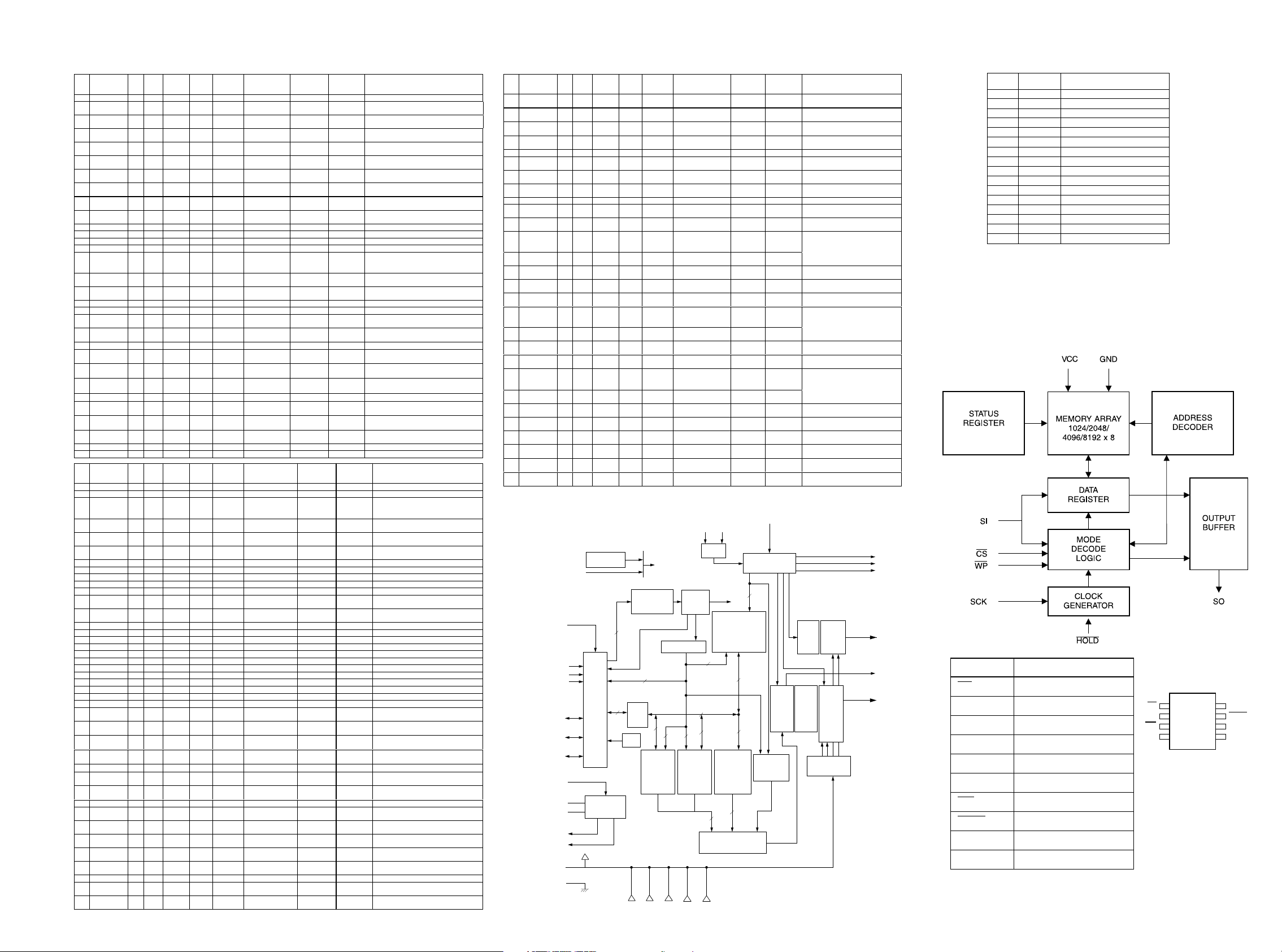
5. MICROPROCESSOR AND IC DATA
PIN
PORT NAME
No.
1Vcc sys --- -- -- -- VCC Connected to the system power supply (+5V).
PB0
2
/TP8/TMO0
PB1
3
/TP9/TMIO1
PB2
4
/TP10/TMO2
PB3
5
/TP11/TMIO3
PB4
6
/TP12
PB5
7
/TP13
PB6
8
/TP14
PB7
9
/TP15
RESO
10
/ /_FWE
11 Vss sys -- -- -- -- VSS Connected to the system power supply (0V).
12 P90/TxD0 O O -- Low -- DEBUG_TXD TXD for debug mode.
13 P91/TxD1 O O -- Low -- FLASH_TXD TXD for FLASH MPU program.
14 P92/RxD0 I I -- Low -- DEBUG_RXD RXD debug mode.
15 P93/RxD1 I I -- High
P94
16
/SCK0/IRQ4
P95
17
/SCK1/IRQ5
18 P40 I/O O -- High OPEN ESA_SDTI RL5C357 SDTI Serial data output for ESA.
19 P41 I/O O -- High OPEN ESA_SCK RL5C357 SCK Serial clock data output for ESA.
20 P42 I/O O -- High OPEN ESA_XLT RL5C357 XLT
21 P43 I/O O Low High OPEN ESA_XSOE RL5C357 XSOE
22 Vss sys -- -- -- -- VSS Connected to the system power supply (0V).
23 P44 I/O O Low High OPEN ESA_XRST RL5C357 XRST
24 P45 I/O O Low High OPEN ESA_XWRE RL5C357 XWRE
25 P46 I/O O Low High OPEN ESA_XQOK RL5C357 XQOK
26 P47 I/O ! - High EXT_DW ESA_SDTO RL5C357 SDTO Serial data input from ESA.
27 P30 I/O
28 P31 I/O I High Low EXT_DW ESA_CHDT RL5C357 CHDT
29 P32 I/O O High Low -- CXD_RW_SEL CXD2585Q LOCK
30 P33 I/O O High Low -- CXD_LDON Laser diode ON/OFF control.
31 P34 I/O I Low -- CXD_FOK CXD2585Q FOK Focus lock detect input.
PIN
PORT NAME
No.
32 P35 I/O I Low Low -- CXD_LOCK CXD2585Q LOCK GFS l ock input.
33 P36 I/O I Low -- CXD_SSTP CXD2585Q SSTP Disc inside detect i nput.
34 P37 I/O O Low High -- CXD_XRST CXD2585Q XRST
35 Vcc sys -- -- -- -- V CC
36 P10 I/O O High Low -- CXD_DOUT_OFF CXD2585Q MD2
37 P11 I/O O High High -- CXD_MUTE CXD2585Q MUTE
38 P12 I/O O -- High -- CXD_DATA CXD2585Q DATA Serial data output for CXD2585Q.
39 P13 I/O O -- High -- CXD_XLAT CXD2585Q XLAT Serial latch data ou tput for CXD2585Q.
40 P14 I/O O -- High -- CXD_CLOK CXD2585Q CLOK Serial cl ock data output. For CXD2585Q
41 P15 I/O O -- High -- CXD_SCLK CXD2585Q SCLK Clock outp ut for SENS serial dat a read.
42 P16 I/O I -- Low -- CXD_SENS CXD2585Q SENS SENS signal inp ut.
43 P17 I/O I -- Low EXT_DW CXD_EMPH CXD2585Q EMPH
44 Vss sys -- -- -- -- VSS
45 P20 I/O I Low High EXT_UP SW_DATA0 KEY INPUT Key matrix signal input.
46 P21 I/O I Low High EXT_UP SW_DATA1 KEY INPUT Ditto.
47 P22 I/O I Low High EXT_UP SW_DATA2 KEY INPUT Ditto.
48 P23 I/O I Low High EXT_UP SW_DATA3 KEY INPUT Ditto.
49 P24 I/O I Low High EXT_UP SW_DATA4 KEY INPUT Ditto.
50 P25 I/O I Low High EXT_UP SW_DATA5 KEY INPUT Ditto.
51 P26 I/O I Low High EXT_UP SW_DATA6 KEY INPUT Ditto.
52 P27 I/O I Low High EXT_UP SW_DATA7 KEY INPUT Ditto.
53 P50 I/O O -- High -- SW_SCAN0 KEY SCAN Key matrix signal output.
54 P51 I/O O -- High -- SW_SCAN1 KEY SCAN Ditto.
55 P52 I/O O -- High -- SW_SCAN2 KEY SCAN Ditto.
56 P53 I/O O -- High -- SW_SCAN3 KEY SCAN Ditto.
57 Vss sys -- -- -- -- VSS
58 P60 I/O O -- Low -- SIF_ST 74HC4094 STR
59 P61 I/O O
60 P62 I/O O
61 P67/ -- -- OPEN PAI System clock output.
62 STBY/ sys I High High EXT_UP STBY
63 RES/ sys I Low High EXT_UP RES
64 NMI sys I -- Low EXT_DW NMI Not used.
65 Vss sys -- -- -- -- VSS
66 EXTAL sys I -- -- -- EXTAL X'tal
67 XTAL sys I -- -- -- XTAL X'tal
68 Vcc sys -- -- -- -- VCC
69 P63 I/O O -- Low -- SIF_CK
70 P64 I/O O -- Low -- DAC_DATA PCM17 10 MD/DM1 Serial data out put for D/A converter IC.
71 P65 I/O O
72 P66 I/O O
DEV
ICE
I/O
I/O O -- Low -- LCD_RS HD66712 RS
I/O O -- High -- LCD_RW HD66712 RW
I/O O -- Low -- LCD_E HD66712 E
I/O O Low High -- LCD_RESET HD66712 RESET
I/O I/O -- Low -- LCD_DB4 HD66712 DB4 LCD driver data bit 0.
I/O I/O -- Low -- LCD_DB5 HD66712 DB5 LCD driver data bit 1.
I/O I/O -- Low -- LCD_DB6 HD66712 DB6 LCD driver data bit 2.
I/O I/O -- Low -- LCD_DB7 HD66712 DB7 LCD driver data bit 3.
sys I Low Low EXT_DW FE W 74HC00
I/O I -- Low EXT_DW SIF_SO 74HC165 Parallel to serial IC (74HC165) data inpu t.
I/O O -- High
DEV
ICE
I/O
Φ
I/O ACTIVE INITIAL
!
Low High EXT_DW ESA_XWIH RL5C357 XWIH
I/O ACTIVE INITIAL
--
--
-- --
--
--
PULL
SIGNAL NAME
UP/DOWN
CXD_SQSO
INT UP
/FLASH_RXD
CXD_SQCK CXD2585Q SQCK Read out clock output for SQSO.
INT UP
PULL
UP/DOWN
Low OPEN SIF_LD 74HC165 LS/
Low -- SIF_SI 74HC4094 DA
Low -- DAC_CLK PCM1710 MC/DM2
Low -- DAC_LAT PCM1710 ML/DSD
SIGNAL NAME
CXD2585Q
/74HC00
CONNECT
DEVICE
NAME
CONNECT
DEVICE
NAME
74HC4094
74HC165CKCK
CONNECT
DEVICE
PORT NAME
SQSO
CONNECT
DEVICE
PORT
FUNCTION
LCD driver register select.
Instruction “L”, Data register “H”
LCD driver READ/WRITE.
READ “H”, WRITE “ L”
LCD driver enable.
Data READ/WRITE active signal.
LCD driver reset.
Normal “H” , Reset “L”
FLASH MPU program enable signal.
Enabled “H”
Sub-Q 80bit/PCM peak level data input &
CD-TEXT data input./RXD for FLASH MPU
program.
Serial latch data output for ESA.
Enabled signal for ESA serial data.
Enable “L ”
System reset output for ESA.
Reset “L ”
Write enable output for ESA.
Enable “L ”
Sub-code Q signal output for ESA.
OK “L”
Write enable signal from ESA.
Disable “L”
Data monitor input from ESA.
Monitoring “H ”
RF gain select for CD-RW
CD-RW “H”, CD-DA & CD-R “L”
FUNCTION
System reset output.
Reset “L”
Connected to the system power supply
(+5V).
Digital audio data output ON/OFF.
ON “H”
Mute control output.
Mute “H”
Emphasis enable/disable input.
Enable “H”, Disable “L”
Connected to the system power supply
(0V).
Connected to the system power supply
(0V).
Serial strobe data out put for serial to
parallel IC (74HC4094) .
Serial load data output for s erial to parallel
IC (74HC4094) .
Serial data output for serial to parallel IC
(74HC4094) .
Standby mode input for MPU.
Normal mode “H”
System reset input for MPU.
Reset “L ”
Connected to the system power supply
(0V).
System clock input.
Connected to 20MHz X' tal.
System clock output.
Connected to 20MHz X' tal.
Connected to the system power supply
(+5V).
Serial clock data output for por ts expand
IC
Serial clock data output for D/A c onverter
IC.
Serial latch data outpu t for D/A converter
IC.
PIN
PORT NAME
No.
73 MD0 sys I -- High EXT_UP MD0
74 MD1 sys I -- High EXT_UP MD1
75 MD2 sys I -- High EXT_UP MD2
76 Avcc sys I -- -- -- AV CC
77 Vref sys I -- -- -- VREF Ditto.
P70
78
/AN0
79 P71/AN1 I I Low High EXT_UP SW_SP1 KEY INPUT
80 P72/AN2 I I Low High EXT_UP SW_FADER KEY INPUT
81 P73/AN3 I I -- High EXT_UP EEPROM_SO AT 2 5 6 4 0 SO Serial data input for EEPROM.
82 P74/AN4 I I -- Low EXT_UP TRAY_SW_OPEN
83 P75/AN5 I I -- Low EXT_UP TRAY_SW_CLOSE
P76
84
/AN6/DA0
P77
85
/AN7/DA1
86 Avss sys I -- Low -- AVSS
P80
87
/IRQ0/
P81
88
/IRQ1/
P82
89
/IRQ2/
P83
90
/IRQ3/
91 P84 I/O O Low Low -- AUDIO_MUTE
92 Vss sys -- -- -- -- VSS
PA 0
93
/TP0/TCLKA
PA 1
94
/TP1/TCLKB
PA 2
95
/TP2/TIOCA0
PA 3
96
/TP3/TIOCB0
PA 4
97
/TP4/TIOCA1
PA 5
98
/TP5/TIOCB1
PA 6
99
/TP6/TIOCA2
PA 7
100
/TP7/TIOCB2
DEV
ICE
I/O ACTIVE INITIAL
I/O
I I Low High EXT_UP SW_SP0 KEY INPUT
I I -- Low UP/DW SYS_MODEL_SEL0 RU09,RU 05
I I -- Low UP/DW SYS_MODEL_SEL1 RU10,RU 11
I/O I -- Low -- CXD_SCOR CXD2585Q SCOR
I/O O Low High EXT_UP MONI_MUTE
I/O O High Low EXT_UP TRAY_DRV_OPEN LB1641 IN2
I/O O High Low EXT_UP TRAY_DRV_CLOSE LB1641 IN1
I/O I Low High EXT_DW ROT_DIAL_A DIAL(+)
I/O I Low High EXT_DW ROT_DIAL_B DIAL(-)
I/O O Low High -- RC5_MASK IR signal mas k SW.
I/O O -- Low -- RC5_OUTPUT RC5 signal output.
I/O I -- Low -- RC5_INPUT SPS-446-4 RC5 signal input.
I/O O High High EXT_UP EEPROM_CS AT2 5 6 4 0 CS
I/O O -- High EXT_UP EEPROM_SI
I/O O -- High EXT_UP EEPROM_CLK
QY01 : HD66712
Reset circuit
ACL
*
RESET
IM
System
*
RS/CS
R/SCLK
RW/SID
DB4~DB7
DB3~DB0
DB0~SOD
Vci
C1
C2
V5OUT2
V5OUT3
V
CC
GND
interface
Serial
4 bits
8 bits
output
buffer
Booster
8
PULL
Address counter
8
3
RAM
SIGNAL NAME
Instruction
decoder
Character
generator
RAM
(CGRAM)
64 bytes
UP/DOWN
Instruction
register
(IR)
8
7
7
Data
register
(DR)
Busy
flag
Segment
(SGRAM)
16 bytes
V1 V2 V3 V4 V5
OSC1 OSC2
7
CONNECT
DEVICE
NAME
TRAY OPEN
SW
TRAY
CLOSE SW
AT2 5 6 4 0
AT2 5 6 4 0
CPG
Timing generator
Display data RAM
(DDRAM)
80x8 bits
7
8
8
Character
generator
ROM
(CGROM)
9,600 bits
5
5/6
Parallel/serial
converter
8
8
and smooth scroll circuit
CONNECT
DEVICE
PORT
Mode select input for MPU.
Mode7 “H”
Mode select input for MPU.
Mode7 “H”
Mode select input for MPU.
Mode7 “H” , FLASH MPU program “L”
Connected to the system power supply
(+5V).
PLAY/PAUSE button input.
Active “L
CUE button input.
Active “L”
FADER SW input.
Active “L”
Tray Open SW input.
Open “L”
Tray Close SW input.
Close “L”
( SEL0,SEL1);
PMD330=(0,0), PMD331=(0,1)
PMD340=(1,0)
Connected to the system power supply
(0V).
Detected from Sub code think signal.
Detected “H”
Audio pre-mute control output.
MUTE “L”
(IN1,IN2), (1,0) CW LOAD,
(0,1) CCW UNLOAD,
(0,0) or (1,1) STOP
Audio mute control output.
MUTE “L”
Connected to the system power supply
(0V).
Rotary encoder input.
CW (Froward) “H ”, CCW (Reverse) “L”
24puls/360˚
Chip select output for EEPROM.
60-bit
shift
register
Enable “H”, Disable “L”
34bit
shift
register
60-bit
latch
circuit
SI Serial data output for EEPROM.
SCK Serial clock data output for EEPROM.
EXT
7
Cursor and
blink
controller
FUNCTION
Common
signal
driver
Segment
signal
driver
LCD drive
voltage selector
CL1
CL2
M
COM0~
COM33
SEG1~
SEG60
D
5 6
Q201/Q202 : TDA7073AQU01 : H8/3062
PIN SYMBOL DESCRIPTION
1 IN1- negative input 1
2 IN1+ positive input 1
3 n.c. not connected
4 n.c. not connected
5 VP positive supply voltage
6 IN2+ positive input 2
7 IN2- negative input 2
8 n.c. not connected
9 OUT2+ positive output 2
10 GND2 ground 2
11 n.c. not connected
12 OUT2- negative output 2
13 OUT1- negative output 1
14 GND1 ground 1
15 n.c. not connected
16 OUT1+ positive output 1
QU03 : AT2560
Page 6
Pin
NO.
37
38
39
40
41
42
43
44
45
46
47
48
49
50
51
52
53
54
55
56
57
58
59
60
61
62
63
64
65
66
67
68
69
70
71
72
I
I
I
I
I
I
I
O
I
O
I
I
I
O
I
O
I
I
I/O
O
I
I
O
O
O
O
O
I
I
O
Analog
-
1, 0
Analog
1, Z, 0
1, 0
1, Z, 0
1, 0
1, 0
1, 0
1, 0
1, 0
Test. Normally, GND.
Center voltage input.
Focus error signal input.
Sled error signal input.
Tracking error signal input.
Center servo analog input.
RF signal input.
Test. No connected.
Analog GND.
Constant current input for operational amplifier.
Analog power supply.
EFM full-swing output. (Iow = Vss, high = VDD)
Asymmetry comparator voltage input.
EFM signal input.
Analog GND.
Multiplier VCO1 control voltage input.
Master PLL filter output (slave = digital PLL).
Master PLL filter input.
Master PLL charge pump output.
Analog power supply.
Asymmetry circuit constant current input.
Wide-band EFM PLL VC02 control voltage input.
Wide-band EFM PLL VC02 oscillation output. Serves as
wide-band EFM PLL clock input by switching with the command.
Wide-band EFM PLL charge pump output.
Digital power supply.
Asymmetry circuit on/off (low = oft, high = on).
Digital Out on/oft control (low = off, high = on).
Digital Out output.
D/A interface. LR clock output. f = Fs
D/A interface. Serial data output (two's complement, MSB first).
D/A interface. Bit clock output.
Outputs a high signal when the playback disc has emphasis, and a low
signal when there is no emphasis.
Crystal selection input. Low when the crystal is 16.9344MHz; high when it is
33.8688MHZ.
Digital GND.
Crystal oscillation circuit input. When the master clock is input externally,
input it from this pin.
Crystal oscillation circuit output.
TES1
VC
FE
SE
TE
CE
RFDC
ADIO
AV
SS
0
IGEN
AV
DD
0
ASYO
ASYI
RFAC
AV
SS
1
CLTV
FILO
FILI
PCO
AV
DD
1
BIAS
VCTL
V16M
VPCO
DV
DD
2
ASYE
MD2
DOUT
LRCK
PCMD
BCK
EMPH
XTSL
DV
SS
2
XTAI
XTAO
Symbol I/O Description
-
-
-
-
-
-
-
-
Pin
NO.
73
74
75
76
77
78
79
80
O
O
O
O
I
I
O
I
1, 0
1, 0
1, 0
1, 0
1, 0
Serial data output in servo block.
Serial data readout clock output in servo block.
Serial data latch output in servo block.
Sub-Q 80-bit, PCM peak or level data outputs. CD TEXT data output.
SQSO readout clock input.
GRSCOR resynchronization input.
Sub-Q P to W serial output.
SBSO readout clock input.
SOUT
SOCK
XOLT
SQSO
SQCK
SCSY
SBSO
EXCK
Symbol I/O Description
Notes)
* PCMD is a MSB first, two's complement output.
* GTOP is used to monitor the frame sync protection status. (High: sync protection window released.)
* XUGF is the frame sync obtained from the EFM signal, and is negative pulse. It is the signal before sync protection.
* XPCK is the inverse of the EFM PLL clock. The PLL is designed so that the falling edge and the EFM signal
Atransition point coincide.
* The GFS signal goes high when the frame sync and the insertion protection timing match.
* RFCK is derived from the crystal accuracy, and has a cycle of 136us. (during normal speed)
* C2PO represents the data error status.
* XROF is generated when the 32K RAM exceeds the +-28F jitter margin.
QD01 : CXD2585Q
Pin
Symbol I/O Description
V16M
XTAI
XTSL
VCTL
VPCO
XTAO
69
60
72
71
27
FSTO
C4M
16
50
RFAC
ASYI
49
ASYO
48
ASYE
62
BIAS
57
12
XPCK
53
FILO
FILI
54
PCO
55
52
CLTV
25
MDP
LOCK
24
PWMI
23
7
SENS
4
DATA
5
XLAT
6
CLOK
SCOR
15
SBSO
79
80
EXCK
SCSY
78
SQSO
76
SQCK
77
RFDC
43
CE
42
TE
41
SE
40
FE
39
VC
38
IGEN
46
QT52 : SN75158
3
1A
5
2A
Generator
Asymmetry
Corrector
Interface
OPAmp
Analog SW
58
Clock
Digital
PLL
Digital
CLV
CPU
59
11
demodurator
Sequencer
A/D
Converter
44
ADIO
XUGF
13
EFM
Servo
Auto
EMPH
GFS
68
10
Sub Code
Processor
FOCUS SERVO
SLED SERVO
2
1
6
7
WFCK
Corrector
SERVO
Interface
MIRR
DFCT
FOK
SERVO DSP
TRACKING
SERVO
1Y
1Z
2Y
2Z
Error
32K
RAM
17
1Z
1Y
1A
GND
WDCK
C2PO
LRCK
65
66
14
D/A
Interface
Digital
OUT
Signal processor biock
PWM GENERATOR
FOCUS PWM
GENERATOR
TRACKING PWM
GENERATOR
GENERATOR
1
2
3
4
MUTE
BCK
PCMD
67
3
Servo block
SLED PWM
8
7
6
5
TES1
37
TEST
36
XRST
2
63
MD2
DOUT
64
73
SOUT
74
SOCK
XOLT
75
SCLK
8
COUT
19
SSTP
26
ATSK
9
MIRR
20
21
DFCT
22
FOK
33
FFDR
34
FRDR
31
TFDR
32
TRDR
29
SFDR
30
SRDR
1A
V
CC
2Z
2Y
2A 7
2A
7 8
No.
1
DV
2
XRST
3
MUTE
4
DATA
5
XLAT
6
CLOK
7
SENS
8
SCLK
9
ATSK
10
WFCK
11
XUGF
12
XPCK
13
GFS
14
C2PO
15
SCOR
16
C4M
17
WDCK
18
DV
19
COUT
20
MIRR
21
DFCT
22
FOK
23
PWMI
24
LOCK
25
MDP
26
SSTP
27
FSTO
28
DV
29
SFDR
30
SRDR
31
TFDR
32
TRDR
33
FFDR
34
FRDR
35
DV
36
TEST
3
5
DD
0
I
I
I
I
I
O
I
I/O
O
O
O
O
O
O
O
Power supply.
System reset. Reset when low.
Mute input (low: off, high: on)
Serial data input from CPU.
Latch input from CPU. Serial data is latched at the falling edge.
Serial data transfer clock input from CPU.
SENS output to CPU.
1, 0
SENS serial data readout clock input.
Anti-shock input/output.
1, 0
WFCK output.
1, 0
XUGF output. MNTO or RFCK is output by switching with the command.
1, 0
XPCK output. MNTI is output by switching with the command.
1, 0
GFS output. MNT2 or XROF is output by switching with the command.
1, 0
C2P0 output. MNT3 or GTOP is output by switching with the command.
1, 0
Outputs a high signal when either subcode sync SO or S1 is detected.
1, 0
4.2336MHz output. 1/4 frequency division output for V16M in CAV-W mode
1, 0
or variable pitch mode.
Word clock output. f = 2Fs. GRSCOR is output by the command switching.
1, 0
O
-
SS
0
I/O
I/O
I/O
I/O
I
I/O
1, Z, 0
O
I
O
-
DD
1
O
O
O
O
O
O
-
SS
1
I
1Y
1
1Z
6
2Y
Digital GND.
Track count ,signal I/O.
1, 0
Mirror signal I/O.
1, 0
Detect signal I/O.
1, 0
Focus OK signal I/O.
1, 0
Spindle motor external control input.
GFS is sampled at 460Hz; when GFS is high, this pin outputs a high signal.
1, 0
If GFS is low eight consecutive samples, this pin outputs low. Input when LKIN=1.
Spindle motor servo control output.
Disc innermost track detection signal input.
2/3 frequency division output for XTAI pin.
1, 0
Digital power supply.
Sled drive output.
1, 0
Sled drive output.
1, 0
Tracking drive output.
1, 0
Tracking drive output.
1, 0
Focus drive output.
1, 0
Focus drive output.
1, 0
Digital GND.
Test. Normally, GND.
2Z
Page 7
Q501 : PCM1710
DIN
CLKO
XTI
XTO
V
2R
CC
OUT
1
2
3
4
5
6
7
8
DD
9
10
11
12
13
R
14
LRCIN
BCKIN
DGND
V
AGND2R
EXT1R
EXT2R
V
AGND1
Input
Interface
Timing
Control
5-Level ∆Σ DAC
Right
Digital
Filter
Noise
Shaper
Mode
Control
5-Level ∆Σ DAC
Left
Low-Pass
Filter-Left
Output
Amplifier
Left
28
27
26
25
24
23
22
21
20
19
18
17
16
15
ML/DSD
MC/DM2
MD/DM1
MUTE
MODE
CKSL
DGND
V
DD
2L
V
CC
AGND2L
EXT1L
EXT2L
L
V
OUT
1
V
CC
PIN NAME NUMBER FUNCTION
Input Interface Pins
LRCIN 1 Sample Rate Clock Input. Controls the update rate (fs).
DIN 2 Serial Data Input. MSB first, right justified format contains a frame of 16-bit or 20-bit data.
BCKIN 3 Bit Clock Input. Clocks in the data present on DIN input.
Mode Controls and Clock Signals
CLKO 4 Buffered Output of Oscillator. Equivalent to fs.
XTI 5 Oscillator Input (External Clock Input). For an internal clock, tie XTI to one side of the crystal oscillator. For an external clock,
tie XTI to the output of the chosen external clock.
XTO 6 Oscillator Output. When using the internal clock, tie to the opposite side (from pin 5) of the crystal oscillator. When using an
external clock, leave XTO open.
CKSL 23 System Clock Select. For 384fs, tie CKSL “High”. For 256fs, tie CKSL “Low”.
MODE 24 Operation Mode Select. For serial mode, tie MODE “High”. For parallel mode, tie MODE “Low”.
MUTE 25 Mute Control. To disable soft mute, tie MUTE “High”. To enable soft mute, tie MUTE “Low”.
MD/DM1 26 Mode Control for Data/De-emphasis. See “Mode Control Functions” on page 11.
MC/DM2 27 Mode Control for BCKIN/De-emphasis. See “Mode Control Functions” on page 11.
ML/DSD 28 Mode Control for WDCK/Double speed dubbing. See “Mode Control Functions” on page 11.
Analog Functions
V
R 13 Right Channel Analog Output.
OUT
L 16 Left Channel Analog Output.
V
OUT
Power Supply Connections
DGND 7, 22 Digital Ground.
V
DD
2R 9 Analog Power Supply (+5V), Right Channel DAC.
V
CC
AGND2R 10 Analog Ground (DAC), Right Channel.
EXT1R 11 Output Amplifier Common, Right Channel. Bypass to ground with a 10µF capacitor.
EXT2R 12 Output Amplifier Bias, Right Channel. Connect to EXT1R.
AGND 14 Analog Ground.
V
CC
EXT2L 17 Output Amplifier Bias, Left Channel. Connect to EXT1L.
EXT1L 18 Output Amplifier Common, Left Channel. Bypass to ground with a 10µF capacitor.
AGND2L 19 Analog Ground (DAC), Left Channel.
2L 20 Analog Power Supply (+5V), Left Channel DAC.
V
CC
8, 21 Digital Power Supply (+5V).
15 Analog Power Supply (+5V).
Q101 : TZA1022
AP5S
AP1S
AP4C
AP3C
AP2C
LG
MI
VGAP
Q251 : BA6856FP
OD5
SYMBOL PIN DESCRIPTION
OD2 1 output photo diode amplifier 2
OD3 2 output photo diode amplifier 3
I/V
FTC
OD4 3 output photo diode amplifier 4
OD5 4 output photo diode amplifier 5
OD1 5 output photo diode amplifier 1
OD1
PWRON 6 power on switch
RF 7 output data signal
OD4
V
V
DDRF
DD
8 RF ampliÞer supply voltage
9 supply voltage
GND 10 ground
OD3
GND
V
DDL
RF
11 ground RF amplifier
12 laser supply voltage
LO 13 current output for the laser diode
OD2
MI 14 Monitor input
n.c. 15 not connected
n.c. 16 not connected
I/V
1k5
RF
AP1S 17 Input photo diode amplifier (satellite)
AP2C 18 Input photo diode amplifier (central)
n.c. 19 not connected
V
DDL
V/I
V/I
V/I
LO
FTC 20 output fast track counting
LG 21 CD/CDRW gain switch
AP3C 22 Input photo diode amplifier (central)
AP5S 23 Input photo diode amplifier (satellite)
AP4C 24 Input photo diode amplifier (central)
V
DDRF
GND
V
DD
GND
RF
PWRON
9 10
Page 8
Q301 : RL5C357
LOGIC
Pin PIN NAME I/O FUNCTION
HL
1 VCC -- POWER SUPPLY -- -2 XQOK Ipu SUB CODE-Q OK SIGNAL FROM CPU -- OK
3 XWRE Ipu WRITE ENABLE SIGNAL FROM CPU -- PERMIT
4 XEMP O READ INHIBIT SIGNAL TO CPU -- INHIBIT
5 XWIH O WRITE INHIBIT SIGNAL TO CPU -- INHIBIT
6 XCAS2 O DRAM CAS2 CONTROL -- --
7 CHDT
O
DATA COMPARATIVE MONITOR SIGNAL
OUTPUT TO CPU
COMPARE
-8 A10 O DRAM ADDRESS 10 -- -9 CLK I 16.9344MHz CLOCK INPUT -- --
10 GND -- GROUND -- -11 DATI Ics AUDIO DATA INPUT -- -12 LRCI Ics AUDIO L/R CLOCK INPUT Lch Rch
13 BCKI Ics AUDIO BIT CLOCK INPUT -- -14 BCKO O AUDIO BIT CLOCK OUTPUT -- -15 LRCO O AUDIO L/R CLOCK OUTPUT Lch Rch
16 DATO O AUDIO DATA OUTPUT -- --
17 XROF Ics RAM OVERFLOW FROM SIGNAL PROCESSOR IC --
OVER
FLOW
18 RFCK Ipu
FRAME CLOCK FROM SIGNAL PROCESSOR IC,
DERIVED FROM THE CRYSTAL ACCURACY
-- --
19 SCOR I
SUB CODE SYNC DETECT SIGNAL FROM
SIGNAL PROCESSOR IC
-- --
20 XRST Ics SYSTEM RESET -- RESET
21 SDTO O SERIAL DATA OUTPUT TO CPU -- --
22 XSOE Ipu
SERIAL DATA OUTPUT PERMISSION SIGNAL
INPUT FROM CPU
--
PERMIT
23 TEST Ipd TEST MODE -- -24 XLT Ics LATCH INPUT FROM CPU -- -25 SDTI Ics SERIAL DATA INPUT FROM CPU -- --
26 SCK Ics
SERIAL DATA TRANSFER CLOCK INPUT FROM
CPU
-- --
27 XCAS1/XOE O DRAM CAS1/OE CONTROL -- -28 XCAS0 O DRAM CAS0 CONTROL -- -29 D2 I/O DRAM DATA 2 -- -30 D3 I/O DRAM DATA 3 -- -31 D0 I/O DRAM DATA 0 -- -32 D1 I/O DRAM DATA 1 -- -33 XWE O DRAM WE CONTROL -- -34 XRAS O DRAM RAS CONTROL -- -35 A9 O DRAM ADDRESS 9
36 A8 O DRAM ADDRESS 8
37 A7 O DRAM ADDRESS 7
38 A6 O DRAM ADDRESS 6
39 A5 O DRAM ADDRESS 5
40 A4 O DRAM ADDRESS 4
41 A0 O DRAM ADDRESS 0
42 A1 O DRAM ADDRESS 1
43 A2 O DRAM ADDRESS 2
44 A3 O DRAM ADDRESS 3
PIN NO. SYMBOL NAME AND FUNCTION
1 STR strobe input
2 D serial input
3 CP clock input
4, 5, 6, 7,14, 13, 12, 11 QP
0
to QP
7
parallel outputs
8 GND ground (0 V)
9, 10 QS
1
,Q S
2
serial outputs
15 OE output enable input
16 V
CC
positive supply voltage
SCK
XROF XLT
BCKI XSOE
LRCI SDTI
DATI SDTO
SIGNAL
PROCESSOR
CPU I/F
I/F
XQOK ADPCM ADPCM
XWRE
ENCODER DECODER
CHDT CPU
XEMP I/F
XWIH DRAM CONTROLLER
DAC
I/F
DATO
LRCO
BCKO
CLK
XRST
TEST
XRAS
XCASO
XCAS1/XOE
XCAS2
XWE
A0 - A10
D0 - D3
Q302 : HY5117400BJ-60
11 12
QU57 QU58 : 74HC165
11
12
13
14
3
4
5
6
1
D
0
D
1
D
2
D
3
D
4
D
5
D
6
D
7
PL
D
CP
215
10
S
CE
QU04 QU56 : 74HC4094
PIN NUMBER SYMBOL FUNCTION
1
2 CP
7 Q
9
Q
7
Q
7
8 GND Ground (0 V)
7
9 Q
10 D
11, 12, 13, 14, 3, 4, 5, 6 D0 to D7Parallel data inputs
15 CE
16 V
PL
Asynchronous parallel load
input (active LOW)
Clock input (LOW to
HIGH, edge-triggered)
Complementary output from
7
the last stage
Serial output from last stage
7
Serial data input
S
Clock enable input
(active LOW)
Positive supply voltage
CC
Page 9

6. WIRING DIAGRAM
SW PCB (P851)
31
J852
31
W802
31
31
J802
LIVE
NEUTRAL
TRANS PCB (P801)
001M
TRAY MOTOR
TRAY OUT
TRAY IN
31
J851
5
4
3
2
1
31
5
4
3
2
TRM+
TRM-
TROU
TRIN
W002
W801
COM
015M
NEUTRAL SIDE
WHT(U,F)
BLUE(N)
LIVE SIDE
RED (U,F)
BROWN(N)
NEUTRAL
J001
FG
LIVE
INSIDE VIEW
W003(ONLY PMD3xxU,PMD340N)
J801
5
5
4
3
2
11
AC9V
AC9V
4
3
AC20V
2
GND
AC20V
1
JM01
5
5
TRM+
4
3
2
1
TRM-
4
3
GND
2
TRAY_SW_OPEN
1
TRAY_SW_CLOSE
W001
3:+12VM
2:GND
1:+6VM
3P PLUG (PMD3xxU,PMD340N)
2P PLUG (PMD33xN,PMD3xxF)
8:SRDR
6:MDP
5:IN DET
4:GND
9:TFDR
7:SFDR
11:FFDR
10:TRDR
12:FRDR
14:VC
13:LD
16:FE
15:RF
17:TE
20:RW
19:+5VA
18:DOUT_OFF
(5PIN FFC)
MAIN PCB (PD01)
8:LCD_E
6:LCD_DB4
5:LCD_DB5
4:LCD_DB6
3:LCD_DB7
2:+5VDM
1:+6VM
9:LCD_RW
7:LCD_RESET
11:IR
10:LCD_RS
JT52
W054
JT03
16:PLAY
12:PLAY_LED
15:PITCH_LED
14:END_LED
13:CUE_LED
17:CUE
54321
54321
+5V
GND
+5V
D_OUT
24:SW_DATA5
22:SW_DATA7
26:SW_DATA3
25:SW_DATA4
23:SW_DATA6
21:SW_SCAN0
20:SW_SCAN1
19:SW_SCAN2
18:SW_SCAN3
XLR PCB (PB01)
(PMD331,PMD340)
JB52
54321
W053
(5PIN FFC)
JB32
GND
29:SW_DATA0
30:GND
28:SW_DATA1
27:SW_DATA2
5432154321
54321
54321
54321
GND
HOT
L
COLD
HOT
COLD
R
ROT_DIAL_B
ROT_DIAL_A
GND
JU02
3
2
1
WY51
3
2
1
VAM1202
(PMD330,PMD331)
VAM1250
(PMD340)
SERVO PCB (P101)
J101
J201
J202
(PMD340)
J102
-15V
+15V
JV01
HEAD PHONE PCB (PV01)
L
-15V
JD01
W051
(20PIN FFC)
JY41
IR SENS PCB (PY41)
R
L
GND
54321
54321
FG
FG
3
2
1
WY41
22
JY02
3
33
2
11
1
JU01
W052
(30PIN FFC)
JY01
+5V
IR
GND
DISPLAY PCB (PY01)
FGFG
+15V
R
GND
J502
54321
54321
WV51
DIAL(-)
DIAL(+)
GND
321
JY51
321
DIAL PCB (PY51)
(PMD331,PMD340)
WY02WY01
WV01 WV02
13 14
Page 10

7. BLOCK DIAGRAM
CDM
VAM1202(PMD330,PMD331)
VAM1250(PMD340)
001M
TRAY LM302
TRAY MOTOR
TRAY OUT
TRAY IN
JU51
RC5 INPUT & OUTPUT
TRM+
TRM-
GND
TROU
TRIN
HF AMP
Q101
TZA1022
(PMD330)
Q101
TZA1022
(PMD331)
Q102
NJM2137M
(PMD340)
MOTOR DRIVER
Q201,Q202
TDA7073AT X2
(PMD330,PMD331)
FOR HALL MOTOR
Q251
BA6856FP
TRAY CONTROL
2,10
Q102,Q103
NJM2100M X2
Q102
NJM2137M
Q103
NJM2100M
Q103
NJM2100M
(PMD340)
QM01
LB1641
5,6
89,90
97
96
XD01
16.9344MHZ
71,72
CD DECODER & DIGITAL SERVO
38-40
43,50
2-8
29-34
22,24,76,77
XU01
20MHZ
66,67
CONTROL U-COM
QU01
H8/3062
29-43
QD01
CXD2585Q
1715
64
18-28
65-67
59
DIGITAL FIL. & DAC
26-28
70-72
2-9
9,17
58,60,69
DRAM(16M)
Q302
HY5117400BJ-60
(PMD331,PMD340)
2-25
ESA
Q301
RL5C357
(PMD331/340)
2-7
20-26 14-16
1-3
Q501
PCM1710
27-44
1-3
13,16
JT02
OPTICAL_OUT
(PMD331,PMD340)
JT01
DIGITAL OUT
OUTPUT AMP
Q502
NJM4560
SO
QU04
74HC4094
11-14
DISPLAY CONTROL & DISPLAY
QY01
LCD DRIVER
HD66712SA02FS
INDICATOR
DY07 TO DY18
LED X10
QY05
LCD
BALANCED
DIGITAL LINE DRIVER
QT52
SN75158P
(PMD331,PMD340)
BALANCED OUTPUT AMP
QB01 TO QB04
NJM4560 X3
(PMD331,PMD340)
HEADPHONE AMP
WITH VOLUME CONTROL
QV01
NJM4556AM
JT53
BALANCED DIGITAL
(PMD331,PMD340)
JB53
BALANCED OUTPUT
(PMD331,PMD340)
JB54
BALANCED OUTPUT
(PMD331,PMD340)
JV02
HEADPHONE OUTPUT
J501
ANALOG LINE OUTPUT
OUTPUT
JU52
FADER START
JU53
GPI (CONTROL I/O)
25PIN
(PMD331,PMD340)
(PMD330)
PISO
QU57,QU58
74HC165 X2
QU56
74HC4094
(PMD331,PMD340)
15 16
80
16,59,69
58,60,69
97
IR SENSOR
QY41
SPS-446-4
93,94
98-100
EEPROM(64K)
FOR CD-TEXT & PRESET
PITCH DIAL
SY51
EC16B24102
(PMD331,PMD340)
78,79
45-56
QU03
AT25640
KEY AND CONTROL INPUT
SY01 TO SY30
POWER SUPPLY
+15VA
-15VA
+5VA
+5VD
+6VM
REGULATOR
Q803
NJM78M15A
Q804
NJM79M15FA
Q801
NJM7805FA
Q802
NJM7806FA
B.DIODE
D802
D2SBA20
D801
D3SB20
SW & FILTER
S851,L851
TRANSFORMER
L801
W001
Page 11

8. SCHEMATIC DIAGRAM
17 18
Page 12

20
0V
RW
19
5.0V
+5VA
DOUT_OFF
FRDR
FFDR
TRDR
TFDR
SRDR
SFDR
TO SERVO PCB (J102 VIA W051)
IN DET
+12VM
+6VM
+5VA
18
0V
17
2.5V
TE
16
2.5V
FE
15
2.5V
RF
14
2.5V
VC
13
5.0V
LD
12
0.3V
11
0V
10
0V
9
0V
8
0V
7
0V
6
2.9V
MDP
5
5.0V
4
GND
3
9.8V
+12VM
2
GND
1
6.0V
+6VM
JD01
001M
LM302
0MA
TRAY MOTOR
TRAY OUT
TRAY IN
RT04
CT04
0.1
75
LT02
1K
CT03
2200p
5.0V
CT08
47/10V
COAXIAL_
OUT
0.5VPP
JT01
OPTICAL_
OUT
JT02
JT03
GND
1
0V
2
D_OUT
3
GND
+5V
4
5.0V
TO XLR PCB (JT52 VIA W054)
+5V
DIGITAL OUT
+5VD
5
PMD331,PMD340 ONLY
+5VD
C304
0.1
5.0V
26
VCC
VSS
1
2.3V
DQ0
DQ1
WE
RAS
A10
A0
A1
2.6V
A2
A3 A4
5.0V
C303
0.1
2
DQ0
2.3V
3
DQ1
5.0V
4
WE
3.6V
5
RAS
6
A11
0V
8
A10
0.8V
9
A0
0.8V
10
A1
11
A2
2.6V
12
A3
VCC VSS
Q302
4X4M
HY5117400BJ-60
DQ3
DQ2
CAS
DRAM
2.5V
25
2.1V
24
4.8V
23
0V
22
OE
0V
21
A9
0V
A8
19
0V
18
A7
0V
A6
17
2.3V
16
A5
2.3V
15
A4
1413
C301
10/16V
MAA
015M
TRM+
5
5
TRM-
4
4
COM
3
3
TROU
2
2
TRIN
1
1
LT01
CT07
0.1
PMD331,
PMD340
ONLY
DQ3
DQ2
CAS
OE
A9
A8 A0
A7
A6
A5
+5VD
DRIVER
QM01
LB1641
JM01
*
0V
5
0V
4
3
TRAY_SW_OPEN
5V
2
TRAY_SW_CLOSE
0V
1
4
12
3
MG
CM01
0.022
DM02
8.2V
DOA
RT02
CT01
220
0.1
RT03
330
LT03
1K
+5VD
ESA
WE
DQ1
DQ3
DQ0
5.0V
2.3V
2.3V
2.5V
33 23
D1D0D3
XWE
34
RAS
XRAS
A9
A9
A8
A8
A7
A7
A6
A6
A5
A5
A4
A4
RL5C357
A0
A1
A1
A2
A2
A3
A3
44
XEMP
XWRE
XQOK
VCC
1
A10
0V
0V
5.0V
C302
0.1
ESA_XQOK
ESA_XWRE
MOTOR
LOGIC
INPUT
5
MG
DQ2
2.3V
D2
Q301
ESA
XWIH
5.0V
ESA_XWIH
RM02
680
CAS
4.8V
678
+5VA
OE
0V
XCAS0
XCAS2
0V
ESA_CHDT
DRIVER
PRE-
+12VM
2
ESA_SCK
0V0V0V
SCK
XOE/XCAS1
A10
CHDT
910
RM01
4.7
1/4W
4700/10V
5V
0V
ESA_SDTI
SDTI
CLK
2.5V
CXD_DOUT_OFF
TRAY_DRV_CLOSE
TRAY_DRV_OPEN
CD05
0.01
CD06
0.47
1500P
CD14
ESA_XLT
C305
0.047
5.0V
XLT
22
TEST
XSOE
SDTO
XRST
SCOR
RFCK
XROF
DATO
LRCO
BCKO
BCKI
LRCI
12
DATI
GND
11
0V
PCMD
RD06
100K
CD08
CD11
0.22
16MHz
PMD330
ONLY
R301
470k
4.9V
0V
5.0V
5.0V
5.0V
2.5V
2.5V
0V
2.5V
2.5V
0.8V
1.2V
RD05
10K
RD09
10K
RD20
1K
CD13
1/16V
T
PMD330
ONLY
CD21
18P
ESA_XSOE
ESA_SDTO
ESA_XRST
XROF
LRCK
EYEPATTERN
CD23
CD07
0.047
2
BCK
CU91
0.1
CD09
1000P
CD10
0.22
1
QD02
CD01
4700P
RD23
CD19
RD08
3.3K
R531
MD2
GND
0V
5.0V
MD2
FWE
RD10
LRCK
0
MONI_MUTE
FWE
+5V
RES
5.0V
5.0V
+5VD
RU28
470K
RES
RD02
15K
CD04
1000P
RD01
2.2k
RD13
33K
CD17
0.1
3.3K
RD07
1M
RD11
22K
LD01LD02
4.7µH4.7µH
PMD330:33P
PMD331:39P
PMD340:39P
BCK
PCMD
0
R532
C515
0.1
C516
10/16V
D502
1SS302
C513
0.1
-15VA
R541
100k
C541
0.1
5.0V
Q541
DTA114YUA
FOR FLASH MPU PROGRAM
RXD
GND
TXD
JU04
12345678
0V
5.0V
5.0V
123
VDD
4
QU91
567
74HC00
91011121314
8
VSS
DEA
RD04
470K
5.0V
2.5V
CD20
150P
CD02
0.047
CD03
1000P
+5VD
R533
CD12
0.1
0
BCK
10/16V
RD03
15K
40
VCFESE
SS
FFDR
FRDR
TES1
TEST
TE
4142434445464748495051525354555657585960
CE
RFDC
ADIO
AV 0
IGEN
AV 0
ASYO
ASY1
RFAC
AV 1
CLTV
FILO
FILI
PCO
AV 1
BIAS
VCTL
V16M
VPCO
SS
DD
SS
DD
5.0V
LD03LD04
0.47µH0.47µH
DV 1
QD02-CD23
RD23
THERMI. 10k
THERMI. 10k
18k
15k
PMD330
PMD331
PMD340
CXD2585Q
CD DECORDER & DIGITAL SERVO
DOUT
PCMD
DV 2DDASYE
MD2
LRCK
BCK
61626364656667686970717273747576777879
RD22
0
EMPH
2.5V
5.0V
z
H
M
4
4
3
.9
6
1
CD15
18P
34
PCMD
LRCK
CXD_EMPH
CXD_DOUT_OFF
DIGITAL FIL. & DAC
Q501
PCM1710
2.5V 5.0V
ML/DSD
1
LRCIN
2.5V
MC/DM2
2
DIN
2.5V
MD/DM1
BCKIN
3
+5VD
2.5V
MUTE
CLKO
4
1.9V
MODE
XTI
5
CKSL
XTO
6
DGND
DGND
7
5.0V
VDD
VDD
8
5.0V
VCC2L
VCC2R
9
20
AGND2L
AGND2R
10
C519
+5VA
1.1VRMS
R544
1k
+5VA
2.5V
C520
10/16V
2.5V
C501
10/16V
R542
2.2k
R543
2.2k
C502
10/16V
EXT1L
EXT1R
11
EXT2L
EXT2R
12
VOUTL
13
VOUTR
AGND1
14 15
R501
10k
R503
4.7k
R502
R504
10k
4.7k
VCC1
1.1VRMS
R505
18k
2SC2878
2SC2878
R506
18k
19
18
17
16
Q542
A/B
Q543
A/B
DAC
FOR DEBUG
JU03
*
12345
RD12
SOCK
C517
0.1
+5VA
C522
FSTO
SOCK
+5VD
C514
0.1
+5VD
MDP
SSTP
XOLT
SQSO
CXD_SQSO
CXD_SQCK
XOLT
JD02
-15VA
5 678
R510
12k
5.0V
RU31
470K
+5VD
PWMI
LOCK
SQCK
SCSY
SOUT
123
SOUT
BAL_OUT(R)
BAL_OUT(L)
VSS
+
-
5.0V
DEBUG_TXD
+5VD
FOK
(XROF)
(RFCK)
SBSO
SOCK
XOLT
SOCK
RB02
10K
ADJ
RB04
220
RB01
10K
ADJ
RB03
220
12k
R509
+
R512
10k
C504
22p
5.0V
DEBUG_RXD
5.0V
RD19
10K
CXD_SSTP
CXD_LOCK
CXD_FOK
21222324252627282930313233343536373839
DFCT
MIRR
COUT
DV 0
WDCK
SCOR
C2PO
XPCK
XUGF
WFCK
ATS K
SCLK
SENS
CLOK
XLAT
DATA
MUTE
XRST
DV 0
EXCK
80
XOLT
RB08
6.8K
1234
VCC
+15VA
RU05XRU10
PMD330
X
PMD331
PMD340
QU03
AT25640
EEPROM
5.0V
VSSSI
SCK
WP
78SO
HOLD
VCC
CS
RU26
10K
RU27
10K
10K
RD17
SS
C4M
CXD_SCOR
GFS
CXD_SCLK
CXD_SENS
CXD_CLOK
CXD_XLAT
CXD_DATA
CXD_MUTE
CXD_XRST
1 2 3 4 5 6 7 8 9 101112 13141516171819 20
DD
0V
RD15
CD18
470K
0.047
+5VD
JD03
123
+5V
GND
GND
FOR ERROR RATE COUNTER
RB07
6.8K
-15VA
VSS
+
+
-
5678
RB06
CB19
22P
C503
22p
R511
10k
C509
Q502
100/16V
NJM4560
C523
100/16V
C510
100/16V
3456
2
1
XROF
RFCK
+5VD
JD04
+15VA
10K
+5VD
RU91
470K
RU92
470K
FLASH_TXD
FLASH_RXD
CXD_SQSO
PMD330:0
PMD331:10K
PMD340:47K
CD22
1000P
PMD340 ONLY
PMD331,
+5VD
5.0V
DD
SFDR
SRDR
TFDR
TRDR
DV 1
100p
100p
QD01
SS
XTSL
DV 2
XTAI
XTAO
SOUT
2.2V
2.2V
XD01
CD16
15P
SOUT
DAC_LAT
DAC_CLK
DAC_DATA
28
5.0V
27
0V
26
C518
25
10/16V
5.0V
24
23
22
21
5.0V
C521
2.5V
10/16V
2.5V
5.0V
10/16V
C505
150p
R507
33k
C507
150p
C524
100/16V
C508
150p
R508
33k
C506
150p
X
0
RU10
X
5.0V
5.0V
5.0V
RU01
10K
TRAY_SW_OPEN
TRAY_SW_CLOSE
PMD330 ONLY
+5VD
DEBUG_TXD
FLASH_TXD
DEBUG_RXD
FLASH_RXD
CXD_SQSO
CXD_SQCK
ESA_SDTI
ESA_SCK
10K
RD18
ESA_XLT
ESA_XSOE
ESA_XRST
ESA_XWRE
ESA_XQOK
RFCK
XPCK
12345
MNT0
MNT1
CB18
22P
CB01
RB05
100/16V
10K
CB12
1234
100/16V
VCC
QB01
NJM4560
NJM4560
CB02
100/16V
+6VM
LCD_DB7
+5VD
LCD_DB6
2
1
345678910 11 12 13 14 15 161718 19
5.0V
5.0V
5.0V
6.0V
+6VM
LCD_DB6
LCD_DB7
+5VD
10K
RU11
0
RU05
SYS_MODEL_SEL1
SYS_MODEL_SEL0
10K
RU02
RU32
FWE
10K
CXD_SQSO
C2PO
XPCK
10K
RD16
XROF
C2PO
GND
MNT2
MNT3
RB09
22K
-15VA
VSS
+
+
-
5678
QB02
+15VA
100/16V
RB12
RB10
22K
R513
22k
R514
22k
C526
0.1
LCD_RESET
LCD_E
LCD_DB4
LCD_DB5
5.0V
5.0V
LCD_E
LCD_RESET
LCD_DB4
LCD_DB5
5.0V
OE
10K
RU09
VDD
STRDACKQ0Q1
12345678
SIF_SI
SIF_ST
+5VD
LCD_RS
LCD_RW
LCD_E
LCD_RESET
LCD_DB4
LCD_DB5
LCD_DB6
LCD_DB7
0V
SIF_SO
AUDIO_MUTE
RB13
4.7K
CB20
22P
RB15
RB11
4.7K
22K
1234
RB19
4.7K
VCC
RB18
4.7K
CB13
22K
CB21
22P
9.8V
D501
ISS301
C525
15.0V
0.1
J502
LCD_RS
LCD_RW
0V
5.0V0V5.0V
LCD_RW
LCD_RS
Q4
OE
74HC4094
SIF_CK
12345678910111213141516171819202122232425
LCD_RS
LCD_RW
LCD_E
LCD_RESET
LCD_DB4
LCD_DB5
LCD_DB6
LCD_DB7
FWE
VSS
DEBUG_TXD
FLASH_TXD
DEBUG_RXD
CXD_SQSO
SIF_SO
CXD_SQCK
ESA_SDTI
ESA_SCK
ESA_XLT
ESA_XSOE
VSS
ESA_XRST
ESA_XWRE
ESA_XQOK
RB17
4.7K
-15VA
CB16
22P
RB14
4.7K
-15VA
RB16
4.7K
RB20
4.7K
+15VA
-15VA
-15.0V
12345
-15V
+15V
IR
PLAY_LED
5.0V
5.0V
IR
Q7
Q5
Q6
Q2Q3VSS
QU04
74HC4094
EEPROM_SI
EEPROM_CLK
99
100
VCC
26272829303133323435363738394041424344454647484950
ESA_SDTO
ESA_XWIH
ESA_CHDT
ESA_SDTO
ESA_XWIH
34
POWER ON
5V
5
0
VSS
+
+
-
5 678
RB23
VSS
+
+
-
5 678
RB24
END_LED
CUE_LED
0V0V0V
910111213141516
QS
QS'
RC5_INPUT
RC5_OUTPUT
RC5_INPUT
EEPROM_CS
(FLASH_RXD)
CXD_RW_SEL
ESA_CHDT
2.0V
4.0V
5.0V
CB14
22P
RB21
4.7K
1234
VCC
+15VA
4.7K
4.7K
RB22
1234
VCC
+15VA
4.7K
CB17
22P
PITCH_LED
CUE
PLAY
5.0V
5.0V
PLAY
CUE
QS
RC5_MASK
ROT_DIAL_B
RC5_MASK
ROT_DIAL_B
RC5_OUTPUT
CXD_LDON
CXD_FOK
CXD_LOCK
CXD_FOK
CXD_LOCK
QU42
DTC114EU
RB25
47
CB03
10/16V
QB03
NJM4560
RB29
4.7K
RB27
47
CB15
22P
RB26
47
CB04
10/16V
QB04
NJM4560
RB30
4.7K
RB28
47
SW_SCAN3
0V
0V
SW_SCAN3
+5VD
ROT_DIAL_A
ROT_DIAL_A
CXD_SSTP
CXD_SSTP
SW_SCAN2
SW_SCAN1
20 21
0V
0V
SW_SCAN2
SW_SCAN1
SW_SCAN0
10K
10K
RU24
RU25
ROT_DIAL_B
RC5_INPUT
AUDIO_MUTE
TRAY_DRV_CLOSE
VSS
AUDIO_MUTE
CONTROL µ-COM
VCC
CXD_XRST
+5VD
CXD_XRST
CXD_DOUT_OFF
CU41
0.1U
RU41
4.7K
0V
RU42
4.7K
RB31
4.7K
CB05
10/16V
100/16V
RB32
4.7K
CB06
10/16V
R515
150
SW_SCAN0
SW_DATA7
22 23
5.0V
5.0V
SW_DATA6
SW_DATA7
10K
RU23
ROT_DIAL_A
MONI_MUTE
TRAY_DRV_OPEN
TRAY_DRV_OPEN
TRAY_DRV_CLOSE
QU01
H8/3062
CXD_MUTE
CXD_DOUT_OFF
CXD_MUTE
CXD_DATA
CB07
100/16V
RB33
10K
RB35
10K
CB09
100/16V
CB08
RB34
10K
RB36
10K
CB10
100/16V
L501
R516
R519
470
R520
0V
0V
L
R
GND
150
470
HEADPHONE OUT
TO HEADPHONE PCB (JV01 VIA WV01)
SW_DATA6
SW_DATA2
SW_DATA3
SW_DATA5
SW_DATA4
24 25 26 27 28 29 30
5.0V
5.0V
5.0V
5.0V
SW_DATA3
SW_DATA4
SW_DATA2
SW_DATA5
10K
10K
10K
10K
RU21
RU19
RU20
RU18
PLAY
CUE
SW_DATA7
SW_DATA6
CXD_SCOR
SYS_MODEL_SEL0
SYS_MODEL_SEL1
AVSS
CXD_SCOR
SYS_PWR_DOWN
SYS_MODEL_SEL0
SYS_MODEL_SEL1
MONI_MUTE
CXD_CLOK
CXD_SCLK
CXD_XLAT
CXD_SENS
CXD_DATA
CXD_CLOK
CXD_SCLK
CXD_SENS
CXD_XLAT
+15VA
+12VM
-15VA
9.8V
+5VA
+5VD
QU41
2SA1036K
+6VM
9.8V
DB01
ISS301
BAL
9.8V
DB02
ISS301
R517
47k
R518
47k
TO DISPLAY PCB (JY01 VIA W052)
JU01
GND
SW_DATA0
SW_DATA1
5.0V
5.0V
SW_DATA0
SW_DATA1
5.0V
10K
10K
10K
10K
10K
10K
RU12
RU14
RU13
RU16
RU17
RU15
SW_DATA0
SW_DATA1
SW_DATA2
SW_DATA3
SW_DATA4
SW_DATA5
CUE
PLAY
SW_FADER
TRAY_SW_OPEN
TRAY_SW_CLOSE
SW_SP0
SW_SP1
SW_FADER
EEPROM_SO
TRAY_SW_OPEN
DAC_LAT
TRAY_SW_CLOSE
DAC_CLK
DAC_DATA
3
4
SW_SCAN3
SW_SCAN2
SW_SCAN1
SW_SCAN0
SW _D ATA 7
SW _D ATA 6
SW_DATA2
CXD_EMPH
SW_DATA1
SW_DATA0
VSS
5.0V
5.0V
5.0V
5.0V
SW_DATA3
SW_DATA0
SW_DATA1
SW_DATA2
SW_DATA3
CXD_EMPH
RES
15.0V
C814
C812
470/16V
0.1
C813
0.1
C815
470/16V
-15.0V
5.0V
C803
0.1
C804
470/10V
NJM7806FA
6.0V
C807
470/10V
C806
MG
0.1
C511
1000p
C512
1000p
+5VD
7677787980818283848586878889909192939495969798
AVCC
VREF
MD2
MD1
MD0
SIF_CK
VCC
XTAL
EXTAL
VSS
NMI
RES
STBY
PAI
SIF_SI
SIF_LD
SIF_ST
VSS
SW_DATA5
SW_DATA4
SW_DATA4
SW_DATA5
NJM78M15FA
Q803
15V
OUT
GND
GND
Q804
-15V
NJM79M15FA
NJM7805FA
Q801
5V
OUT
GND
Q802
6V
OUT
GND
LB01
LB02
2VRMS
2VRMS
SW_FADER
RC5_OUTPUT
IR
RC5_MASK
RC5_INPUT
SIF_CK
5.0V
SIF_SI
SIF_LD
SIF_ST
DA227
51 52 53 54 55 56 57 58 59 60 61 62 63 64 65 66 67 68 69 70 71 72 73 74 75
OE
5.0V
IN
INOUT
IN
IN
DU02
TO ROTARY PCB (JY51 VIA WY51)
PMD331,
JU02
GND
ROT_DIAL_A
ROT_DIAL_B
*
PMD340
123
ONLY
5.0V
5.0V
DU51
ROT_DIAL_B
ROT_DIAL_A
ISS301
4.7V
QU52
DTC114EU
5.0V
4.7V
MD2
CU03
0.1
CU01
15P
CU02
15P
RES
5
0.1
CU04
SW_SCAN3
SW_SCAN2
SW_SCAN1
SW_SCAN0
SW_DATA7
SW_DATA6
+5VD
R804
4.7k
R803
4.7k
Q806
DTC114EU
-25.0V
C801
6800/16V
00/16V
00/16V
JB32
*
R
BALNCED OUT
GND
TO XLR PCB (JB52 VIA W053)
L
J501
*
OE
25.3V
9.8V
9.8V
ONLY
RU07RU08
470K470K
RU06
470K
DAC_LAT
DAC_CLK
DAC_DATA
+5VD
2.2V
2.2V
XU01
20.000MHz
RU04
470K
+5VD
DU01
DA227
5.0V
DU03
ISS301
C808
2200/35V
C810
0.1
C811
0.1
C809
2200/35V
+12VM
C802
0.1
C805
0.1
PMD330:
PMD331:100
PMD340:100
16DBU
PMD331,PMD340
COLD
1
HOT
2
3
COLD
4
HOT
5
16DBU
L
RCA OUT
R
O-END
O-INDEX
SIF_SO
NEXT
PREV
END
PITCH+
PAUSE
STOP
+5VD
+5VD+5VD
PLAY
CUE
0V
D802
D2SBA20
D801
D3SB20
4.8V
RU22
470K
SU51
SSSU
EXTINT
+5VD
RU30
1M
CU05
1/50V
910111213141516
QS
QS'
Q7
Q6
Q5
Q4
OE
VDD
91011121314
QH
S-IN
A
B
C
D
INH
1516
VDD
91011121314
QH
S-IN
A
B
C
D
INH
1516
VDD
Q805
DTC114EU
PDC
(
PMD3XXU, PMD340N
DU52
ISS301
QU51
2SC4081(Q,R)
VSS
78
Q3
6
Q2
5
Q1
4
Q0
3
CK
74HC4094
QS
2
DA
SIF_ST
1
STR
QU56
VSS
78
QH
6
H
5
G
PITCH_SW
4
F
74HC165
PITCH-
3
E
2
CK
1
L
S/
QU57
VSS
78
QH
INDEX-
6
H
INDEX+
5
G
FR
4
F
74HC165
FF
3
E
2
CK
1
L
S/
QU58
C816
1/50V
WHT(U,F)
BLUE(N)
L851
W002
W003
O-FADER
O-PAUSE
SIF_LD
J802
J852
RU53
18K
O-CUE
O-PLAY
13.2V
13
)
SIF_CK
RU55
RU52
47K
31
1K
R805
4.7k
9V
13
13
13
13
J851
NEUTRAL
LIVE
INSIDE VIEW
D803
ISS301
W802
LIVE SIDENEUTRAL SIDE
RED (U,F)
BROWN(N)
S851
*
J001
DTA114YUA
O-END
O-INDEX
O-FADER
PITCH_SW
PITCH-
PITCH+
END
PREV
NEXT
INDEX-
INDEX+
FR
FF
STOP
CUE
O-CUE
PAUSE
O-PAUSE
PLAY
O-PLAY
SW PCB (P851)
LCA
+5VD
QU55
+5VD
RU74
RU73
RU72
RU71
RU70
RU69
RU68
RU67
RU66
RU65
RU64
RU63
RU62
RU60
R801
4.7k
MAIN PCB (PD01)
12345
J801
12345
*
W801
*
12345
20V
20V
L801
U801
U802
PDT
TRANS PCB (P801)
PAC
C851
0.01
3P PLUG (PMD3XXU, PMD340N)
2P PLUG (PMD33XN, PMD3XXF)
W001
+5VD
RU58
10K
+5VD
CU53
RU54
47
QU53
DTA114YUA
CU51
10/16V
RU51
5.0V
PMD330
*
5.0V
0.1
0
ONLY
FADER
IN
JU52
JU51
0V
RC5
PMD331,
PMD340
47K
47K
47K
47K
47K
U
N
F
47K
RU85
1000P
CU67
47K
47K
RU86
RU87
1000P
1000P
CU69
CU68
QU59
DTC114EU
DTC114EU
U801 U802
47K
RU89
RU88
1000P
1000P
CU71
CU70
CU61
1000P
QU60
QU61
DTC114EU
DTC114EU
X
X
X
47K
RU90
1000P
CU72
CU63
1000P
QU62
DTC114EU
47K
47K
RU93
RU94
1000P
1000P
CU74
CU73
CU65CU66
1000P1000P
QU63
QU64
DTC114EU
47K
RU95
1000P
CU75
1000P
CU76
ONLY
JU53
CU80
0.1U
+5VD
GPI PORT
13
FG
25
COMMON
5.0V
12
+5V
24
END TALLY
11
INDEX TALLY
23
FADER(INVERT)
10
FADER(NORMAL)
22
FADER TALLY
9
PITCH ON OFF
21
PITCH-
8
PITCH+
20
END
7
PREVIOUS
19
NEXT
6
INDEX-
18
INDEX+
5
FR
17
FF
4
STOP
16
CUE
3
CUE TALLY
15
PAU SE
2
PAUSE TALLY
14
PLAY
1
PLAY TALLY
CU60
1000P
CU62
1000P
CU64
1000P
CU77
1000P
CU78
1000P
CU79
1000P
47K
RU83
RU80
RU82
RU84
RU81
1K
1K
1K
1K
1K
1K
1K
1K
1K
1K
1K
1K
1K
1K
19 20
Page 13

VSS
VCC
8765
43 21
+
-
+
-
VSS
VCC
8765
43 21
+
-
+
-
VHP
WIN2
WIN1
VIN1
VHN
UIN1
VIN2
UIN2
UOUT
VOUT
WOUT
11
10
9
8
7
6
5
4
3
2
1
IN2-
IN2+
IN1+
IN1-
OUT1+
OUT2-
OUT1-
OUT2+
G1
G2
N.C
VP
NC
NC
NC
NC
-++-
16
15
14
13
12
11
10
9
8
7
6
5
4
3
2
1
IN2-
IN2+
IN1+
IN1-
OUT1+
OUT2-
OUT1-
OUT2+
G1
G2
N.C
VP
NC
NC
NC
NC
-++-
16
15
14
13
12
11
10
9
8
7
6
5
4
3
2
1
RNF
FIN
VM1
VM2
VCC
REV
PS
EC
ECR
CNF
VH
FG1
FG2
FG3
NCH3-
H3+
H2+
H2-
H1-
H1+
GND
A1
NC
A2
NC
A3
NC
NC
26
28
27
25
24
23
22
21
20
19
18
17
16
15
14
13
12
11
10
9
8
7
6
5
4
3
2
1
SLED_MSLED_M+
GND
SLED_SW
4
3
2
1
RAD-
RAD+
FOC-
FOC+
RW
FTC
D2
D3
D4
D5
D1
LDON
RF
VDD
GND
VSUB
16
15
14
13
12
11
10
9
8
7
6
5
4
3
2
1
DOUT_OFF
GND
GND
+6VM
+12VM
IN DET
20
19
18
17
16
15
14
13
12
11
10
9
8
7
6
5
4
3
2
1
SFDR
MDP
SRDR
TFDR
TRDR
FFDR
FRDR
LD
VC
RF
FE
TE
+5VA
RW
RED
0MB
501M
502M
DISK M.
4
3
2
1
VAM1250
11
10
9
8
7
6
5
4
3
2
1
16
15
14
13
12
11
10
9
8
7
6
5
4
3
2
1
SLED M.
SLSW
TT+
TT-
GND
BLK
GRN
YEL
SLEDGE SW
R217
R216
Q203
C103
C110
R114
C214
C201
R206
R209
C258
R251
R252
R255
R253
R254
R262
R263
C255
C256
C257
R265
R264
C252
R256
C251
R258
C254
C253
R257
R266
R261
R260
R259
C104
C109
Q110
J102
Q251
J201
Q252
R113
R125
C120
C108
C216
R215
R205
R204
R201
R202
R116
Q109
C105
R134
R135
C118
R208
R207
C106
C113
C114
C115
C213
C205
C208
C212
C211
C210
C209
C204
C217
R203
C107
R109
R110
R106
C101
C102
Q108
C202
R107
R104
Q103
Q102
Q104
Q107
Q105
C112
C111
R123
Q106
R121
R111
R112
R108
R105
R103
R101
R102
R124
R118
R117
R214
J101
Q202
Q201
C207
C203
J202
15k
12k
10K
27p
22p
0
0.22
1000p
33k
18k
0.047
(1/10W)
82
(1/10W)
82
6.8k
6.8k
6.8k
22k
22k
0.1
0.1
0.1
0
22k
0.1
100k
0.1
10k
100/10V
0.1
10k
(1/10W)
2.2
(1/10W)
2.2
(1/10W)
2.2
(1/10W)
2.2
0.01
0.01
DTC114EU
BA6856FP
2SA1036K
5.6k
8.2k
0.01
100p
0.01
15k
180k
180k
68k
68k
220k
10K
0.1
10k
8.2k
100p
220k
220k
0.1
0.1
47/10V
0.1
470p
4700p
0.1
1000p
1000p
1000p
1000p
0.1
0.47
2.7k
100p
470k
10k
15k
27p
220p
DTA114YUA
1000p
1k
22k
NJM2100M
NJM2137M
DTC114EU
DTC114EU
DTC114EU
100/10V
100/10V
100k
2SA1036K
100k
33k
33k
1.5k
47k
22k
680
680
1k
1k
1k
10k
TDA7073AT
TDA7073AT
100/10V
100/10V
+6VM
+5VA
+5VA
+6VM
+6VM
+5VA
MG
MG
MGMGMG
MG
MG
MG
MG
MGMGMG
MG
MG
MG
MG
MG
MG
MG
MG
MG
MG
MG
MG
MG
MG
MG
MG
MG
MG
+5VA
+5VA
+12VM
+12VM
+5VA
0VMG0VMG0V
MG
Q109
10K
1.2V
0.8V
1
1
EYEPATTERN
TO MAIN PCB (JD01 VIA W051)
SEA
SER
SERVO PCB (P101)
LTOH30PA
LASER
MONITOR
PMD330, PMD331 ONLY PMD340 ONLY
VAM1202
4.7k
330
0.22
6.8
BC808
SLED M.
DISK M.
SLEDGE SW
0MB
501M
BC858
LASER
RADIAL
SEA
C107
100p
R110
10k
10k
8.2k
R135
10k
R134
DTC114EU
R209
18k
MG
R212
Q107
C204
0.1
R113
5.6k
R106
18k
C108
100p
R109
470k
1234
VSS
+
+
-
5678
VCC
R116
220k
C110
22p
C120
0.01
+6VM
C203
100/10V
MG
MG
R208
220k
R207
220k
C207
100/10V
MG
R213
MG
R136
C101
0
---
---
Q204
---
TC4S66F
R206
33k
C217
0.47
Q204
C113
+5VA
Q101
TZA1022
LOMIVDDL
GNDRF
NC
NC
VDDRF
AP1S
AP2C
PWRON
NC
R126
3.3k
FTC
R127
3.3k
LG
AP3C
AP5S
AP4C
R131
10k
+5VA
C114
47/10V
OUT2+
9
10
G2
11
NC
12
OUT2-
13
OUT1-
14
G1
15
NC
16
OUT1+
TDA7073AT
OUT2+
9
10
G2
11
NC
12
OUT2-
13
OUT1-
14
G1
15
NC
16
OUT1+
TDA7073AT
Q102
Q203 R216
---
C117
DTC114EU
-+ +-
Q201
-+ +-
Q202
R101 R102
680
0
12k
R128
3.3k
R130
3.3k
J101
D4
D5
D3
D2
D1
MI
LO
GND
RAD(+)
FOC(-)
FOC(+)
FOCUS
RAD(-)
220k
BC858
0.1
MONITOR
WHT
SLSL+
BLU
YEL
TT-
GRN
TT+
ORG
SLSW
BLK
GND
1
2
3
4
5
6
7
8
9
10
11
12
6
6
5
5
4
4
3
3
2
2
1
1
W041
502M
J201
XH-6
MG
SER
R129
3.3k
PMD330
PMD331
PMD330
PMD331
C115
0.1
MG
MG
MG
MG
NJM2100M --NJM2137M
10k TH
0.1
C116
GND
VDD
RF
OD1
OD5
OD4
OD3
OD2
R121
100k
R112
33k
R111
R125
8.2k
Q109
33k
C118
0.1
Q105
Q106
2SA1036k
R123
100k
R124
1k
8
N.C
7
IN2-
C201
6
IN2+
5
VP
4
C209
3
2
1
8
7
6
5
4
3
2
1
1000p
MG
C211
1000p
C205
4700p
C213
470p
MG
C206
4700p
C215
470p
MG
R132
0 ---
---
C201
4700p
1000p
C210
1000p
MG
C202
1000p
C212
1000p
MGMG
C208
0.1
R133
0 27p
C214
0.47
0.22
NC
NC
IN1+
IN1-
N.C
IN2-
IN2+
VP
NC
NC
IN1+
IN1-
0
680
R217
8.2k
15k
R132
C101
R101
R136
R133
C102
1234
VSS
+
+
Q102
-
5678
1
VCC
C119
0.1
C106
R103
22k
22k
1k
R104
R107
Q103
NJM2100M
100/10V
100/10V
0.1
R216
R210
R211
0.1
1.5k
R108
C105
R117
C111
1k
C112
R118
1k
R217
R203
C214
2.7k
R204
180k
R205
R215
180k
15k
+6VM
0
+6VM
C218
MG
C119
C103
C102
---
220p
R210
22k
0
10p
27p
---
R212
R213
1k
---
4.7k
21 22
C103
47k
R105
R137
0
R114
Q203
R202
68k
R201
68k
2p
1k
C218
---
0.1
Q110
--- 0
DTC114EU
1
R102
DTA114YUA
Q104
DTC114EU
Q110
R214
C216
R114
47k
EYEPATTERN
0.8V
1.2V
Q108
+5VA
MG
+6VM
+5VA
10k
0.01
SERVO PCB (P101)
C118
100p
47p
C109
C104
0.01
0.01
0V
5.0V
0V
2.5V
2.5V
2.5V
2.5V
5.0V
0.3V
0V
0V
0V
0V
0V
2.9V
5.0V
6.0V
J102
1
RW
2
+5VA
3
DOUT_OFF
4
TE
5
FE
6
RF
7
VC
8
LD
9
FRDR
10
FFDR
11
TRDR
12
TFDR
13
SRDR
14
SFDR
15
MDP
16
IN DET
17
GND
18
+12VM
19
GND
20
+6VM
TO MAIN PCB (JD01 VIA W051)
Page 14

QT52
PB01
PY01
PY01
QY01
QY02
QY07 QY08
QY09QY06
QY41
PY41
1
2
3
4
5
TO MAIN PCB (J502)
WV51
1
+15V
-15V
2
3
4
5
JV01
1
2
3
L
4
GND
5
R
HEAD PHONE PCB (PV01)
CV02
100/16V
CV01
100/16V
RV09
50k(A)
RV03
10k
VSS
+
-
5678
RV04
10k
RV02
+
15k
RV01
15k
1234
NJM4556AM
VCC
QV01
CV03
47/16V
RV06
120 1/2W
CV04
47/16V
HPA
RV05
120 1/2W
RV08
4.7k
RV07
4.7k
WV01
WV02
JV02
*
HEDPHONE
5VRMS
9. PARTS LOCATION
5
4
3
2
1
TO MAIN PCB (JT03)
5
4
3
2
1
TO MAIN PCB (JB32)
W054
W053
DIGITAL LINE DRIVER
QT52
LT52
SN75158P
CT53
0.022
5.0V
3.9V
8
1
0V
3.9V
2
7
0V
3
6
0V
4
5
0.1
0V
CT52
220/6.3V
JT52
*
1
1
+5V
2
2
+5V
3
3
GND
4
4
D_OUT
5
5
GND
DOT
DOB
JB52
*
1
1
L
2
2
3
3
GND
4
4
R
5
5
CT56
0.01
CT57
0.01
LT53
*
PULSE TRANSE
1:1
RT52
RT53
LT54
56
*
LT55
56
*
CT58
CT59
220p
220p
16DBU
16DBU
JT53
0V
12
0V
COLD
JB55
JB53
12
COLD
JB54
12
COLD
3
3
3
DIGITAL
HOT
L
HOT
R
HOT
XLR PCB (PB01)
PMD331,PMD340 ONLY
PV01
QV01
PY51
23 24
Page 15

PD01
Q301 Q302 QU04 QD01 QM01
Q501 Q541 QU41 QU42
Q502 QB03 QB02 QB04 QU01 Q803
QB01 QU91 QU03 Q806 Q805 QU58 QU57 QU56
Q802 Q801
Q804
QU52 QU51 QU64 QU63 QU62 Q61 QU60 QU59
25 26
Page 16

POS.
NO
VERS.
COLOR
PART NO.
(FOR PCS)
DESCRIPTION
PART NO.
(MJI)
POS.
NO
VERS.
COLOR
PART NO.
(FOR PCS)
DESCRIPTION
PART NO.
(MJI)
001B BLACK FRONT PANEL PMD330 BLK 371K248010
001B GRAY 9965 000 01604 FRONT PANEL PMD330 GRAY 371K248020
001B BLACK FRONT PANEL PMD331 BLK 371K248110
001B GRAY 9965 000 01726 FRONT PANEL PMD331 GRAY 371K248120
001B BLACK FRONT PANEL PMD340 BLK 371K248210
001B GRAY 9965 000 01721 FRONT PANEL PMD340 GRAY 371K248220
003B BLACK FRONT CHASSIS PMD330 BLK 371K105020
003B GRAY 9965 000 01605 FRONT CHASSIS PMD330
GRAY
371K105030
003B BLACK FRONT CHASSIS BLACK
PMD331/N,/U, PMD340/N
371K105040
003B GRAY 9965 000 01722 FRONT CHASSIS PMD331/340
GRAY
371K105050
003B 340/U FRONT CHASSIS PMD340 USA
BLACK
371K105060
005B BLACK WINDOW BLK 371K158010
005B GRAY 9965 000 01606 WINDOW GRAY 371K158020
006B 9965 000 01607 IR LENS 371K355020
007B BLACK ESCUTCHEON 292K063220
007B 340/U ESCUTCHEON PMD340 USA 292K063260
007B GRAY 9965 000 01608 ESCUTCHEON 292K063230
009B BLACK POWER BUTTON 371K270150
009B GRAY 9965 000 01609 POWER BUTTON 371K270160
010B BLACK BUTTON 371K270170
010B GRAY 9965 000 01610 BUTTON 371K270180
011B LCD SHEET
012B BLACK ROTARY KNOB PMD331/340
BLACK
372K154010
012B GRAY 9965 000 01723 ROTARY KNOB PMD331/340
GRAY
372K154020
013B LCD SPACER
015B LCD HOLDER
016B INSULATOR FOR 015B
017B LCD REFLECTOR
019B LCD LENS
020B WEIGHT FOR KNOB
021B BRACKET FOR PHONE JACK
023B BLACK KNOB FOR PHONE VOLUME 284T154310
023B GRAY 9965 000 01611 KNOB FOR PHONE VOLUME 284T154050
027B 9965 000 01612 BUTTON RUBBER 371K270010
029B 9965 000 01614 BUTTON MODE KEY 371K270020
031B 9965 000 01615 BUTTON END KEY 371K270030
033B 9965 000 01616 BUTTON A-B KEY 371K270040
035B 9965 000 01617 BUTTON PITCH KEY 371K270050
037B 9965 000 01618 BUTTON +/- KEY 371K270070
039B 9965 000 01619 BUTTON NEXT/PREV KEY 371K270080
041B 9965 000 01620 BUTTON FF/FR KEY 371K270090
043B 9965 000 01621 BUTTON STOP KEY 371K270100
045B 9965 000 01622 BUTTON CUE KEY 371K270110
047B 9965 000 01623 BUTTON PLAY KEY 371K270120
001D /U1B LID TOP COVER BLACK 292J257030
003D /U1B MOUNT BRACKET L 371K160040
005D /U1B MOUNT BRACKET R 371K160050
001G CHASSIS
003G SIDE BRACKET L
007G SIDE BRACKET R
011G 9965 000 01624 LEG BLACK 371K057010
012G BUFFER FOR LEG 371K056020
015G LOADER BRACKET
026G BRACKET FOR PD01
030G SUPPORT FOR PD01
031G SUPPORT FOR P801
037G 4822 402 10913 LINK 318K121010
039G /U SCREW FOR GND
045G LABEL FOR GND
060G SHEET
062G STICKER
092G INNER LASER CAUTION
094G LABEL LASER CAUTION
901G REAR PANEL
907G LABEL
909G B.H. TAP. SCREW
911G PH.TAP.SCREW
001M 9965 000 01625 NEW LOADER LM302
OLD TRAY BLK
305K304680
005M 4822 464 10054 FRAME K 305K401500
010M 4822 361 21741 MOTOR MM0030002R
015M 4822 321 63208 CABLE YB00380590
016M 4822 271 30873 MINI SWITCH SM01020620
020M 4822 522 33521 GEAR 305K058030
021M 4822 528 81537 PULLEY 305K262010
025M 4822 522 33522 GEAR K 305K058500
030M 4822 358 31325 BELT 305K264010
031M 4822 459 50976 MASK 305K303010
035M 4822 443 51265 CASE 305K064110
036M 9965 000 01626 SUSPENSION 371K056010
040M 4822 402 11212 NEW LIFT ARM 305K002050
043M 9965 000 00234 CASE K NEW GEAR/OLD TRAY 305K064600
045M CASE BLACK 305K064010
046M SPRING 305K115010
050M CAM 305K054010
051M NEW SLIDER GEAR 305K058050
060M 4822 492 33495 SPRING 305K115020
501M 330,331 9965 000 01627 MECHANISM VAM 1202
9305 022 20200
371K304500
501M 340 9965 000 01724 MECHANISM VAM 1250
9305 022 25001
374K304500
510M BRACKET
518M STOPPER FOR DISC 371K114010
520M STOPPER FOR DISC 371K114020
522M ADHESIVE FOR 520M 371K122010
555M 330,331 CLAMPER ASSY VAM1202 371K005500
555M 340 9965 000 01725 CLAMPER ASSY VAM1250 374K005500
J001 /F 9965 000 01313 JACK 2P AC INLET M1910-H YJ04002440
J001 /N 9965 000 01313 JACK 2P AC INLET M1910-H YJ04002440
J001 /U JACK 3P AC INLET M1910-D YJ04002450
W051 9965 000 01602 JUMPER LEAD 20P FFC YU20170500
W052 9965 000 01603 JUMPER LEAD 30P FFC YU30170520
W053 331,340 JUMPER LEAD 5P FPC YU05090500
W054 331,340 JUMPER LEAD 5P FPC YU05090500
PACKING
001T /F USER MANUAL 371K851110
001T /N 9965 000 01628 USER MANUAL 371K851310
001T /U USER MANUAL 371K851250
W001 /F MAINS CORD 2P 12A 125V ZC02001180
W001 330/N
331/N
4822 321 11439 MAINS CORD 2P 10A 250V
CLASS2
ZC01803080
W001 340/N 4822 MAINS CORD 3P 10A 250V
CLASS1
ZC02003180
W001 /U MAINS CORD 3P 10A 125V ZC02002180
NOT STANDARD
SPEAR PARTS
001S 330 PACKING CASE PMD330 371K801010
001S 331 PACKING CASE PMD331 372K801010
001S 340 PACKING CASE PMD340 374K801010
003S CUSHION 371K809010
W004 /U AUDIO CABLE ZD01000330
NOTE : =PART IS LISTED FOR REFERENCE ONLY, MARANTZ WILL NOT SUPPLY THESE PARTS.
P101 (PMD330, PMD331)
Q110 Q108 Q112
Q107 Q106 Q103 Q102
Q105 Q111 Q201 Q101 Q204 Q202
10. EXPLODED VIEW AND PARTS LIST
P101 (PMD340)
Q107 Q106 Q103 Q102
P851
Q110 Q108 Q112
Q105 Q111 Q202 Q201
Q251 Q204 Q252
P801
27 28
Page 17

SYMBOL
5110
5127
5128
5404
5405
P801
+B. H. M. SCREW
+B. H. TAP TI TE SCREW( W/ )
+B. H. TAP TI T E SCREW( B TYPE)
UONLY
5127
3X8( M)
x3
J001
W001
907G
FONLY
N( PMD33 0
/331) ONLY
W0 0 1
N(PMD340)
ONL Y
518M
007B
001B
003D
MECHA ASSY.
510M
5128
3X6( M)
5128
3X6( M)
001M
5128
3X8( M)
522M
015M
5128
3X6( M)
005B
001D
520M
006B
PY41
005D
021B
009B
JV02
016B
010B
015B
PV01
QY0 5
011B
029B
043B
JY03
031B
045B
037G
019B
033B
017B
L801
003G
013B
035B
027B
015G
USA ONLY
039G
045G
026G
092G
UONLY
094G
UONLY
PY01
PY51
( PMD331, PMD340 ONLY )
012Gx4
031Gx2
030Gx3
007G
011Gx4
PD01
P851
PMD331,
PMD340
ONLY
PMD330
ONLY
001G
NONLY
UONLY
CASE ASSY.
5127
3X8( M)
911G
PB01
x4
5127
2. 6X8( M)
901G
909G
x6
JB53
JB54
JT53
PMD331,
PMD340
ONLY
023B
PMD330
ONLY
037Bx2
039B
020B
012B
( PMD331, PMD340 ONLY )
( PMD331, PMD340 ONLY )
047B
0
41B
003B
062G
( PMD331, PMD340 ONLY )
060G
( PMD331, PMD340 ONLY )
PMD330
ONLY
P101
5128
3X8( M)
29 30
5128
3X8( M)
Page 18

11. TECHNICAL DESCRIPTION
Name
Active
1 PLAY TALLY O Low
2 PAUSE TALLY O Low
3 CUE TALLY O Low
4STOP I Low
5FR I Low
6INDEX- I Low
7PREVIOUS I Low
8PITCH+ I Low
9 PITCH ON/OFF I Low
FADER(NORMAL) I Low
INDEX
#2/
#3 TALLY
OLow
+5V - --FG COMMON - --PLAY I Low
PA US E I L o w
CUE I Low
FF I Low
INDEX+ I Low
NEXT I Low
END I Low
PITCH- I Low
FADER TALLY O Low
FADER(INVERT) I High
END TALLY O Low
TALLY COMMON - ---
1. RC5 Code
This product is able to communicate to the other MARANTZ
products with the RCA Pin cable.
Command Name Code
Play 2053 20 53 11 10100 110101
Pause 2048 20 48 11 10100 110000
Cue 2059-10 20 59 10 11 10100 111011 1010
Stop 2054 20 54 11 10100 110110
FF 2052 20 52 11 10100 110100
FR(REW) 2050 20 50 11 10100 110010
Index+ 2034 20 34 11 10100 100010
Index- 2035 20 35 11 10100 100011
Next 2032 20 32 11 10100 100000
Previous 2033 20 33 11 10100 100001
Pitch+ 2038 20 38 11 10100 100110
Pitch- 2039 20 39 11 10100 100111
Pitch Bend+ 2038-10 20 38 10 11 10100 100110 1010
Pitch Bend- 2039-10 20 39 10 11 10100 100111 1010
A-B 2059 20 59 11 10111 111011
Program 2041 20 41 11 10100 101001
Pitch On/Off 2037 20 37 11 1010 100101
Open/Close 2045 20 45 11 10100 101101
INPUT
Time 2011 20 11 11 10100 1011
Mode 2036-10 20 36 10 11 10100 100100 1010
Preset 2041-12 20 41 12 11 10100 101001 1100
END monitor 2043-10 20 43 10 11 10100 101011 1010
CD-TEXT 2088 20 88 10 10100 11000
SERVICE 166363 16 63 63 11 10000 111111 111111
Connect 1856 18 56 11 10010 111000
Disconnect 1857 18 57 11 10010 111001
OUTPUT
1 The service code is available during STOP mode only.
*
2 The Pitch Bend+ and Pitch Bend- are not available with
*
the digital out on.
3 The Pitch Bend+ and Pitch Bend- are not available on
*
PMD330.
2 3
*
*
3
2
**
0 2000 20 00 11 10100 0
1 2001 20 01 11 10100 1
2 2002 20 02 11 10100 10
3 2003 20 03 11 10100 11
4 2004 20 04 11 10100 100
5 2005 20 05 11 10100 101
6 2006 20 06 11 10100 110
7 2007 20 07 11 10100 111
8 2008 20 08 11 10100 1000
9 2009 20 09 11 10100 1001
1
*
5. GPI code
The GPI code is input from external controller with D-Sub 25
Pin connector.
Decode Binary
SYS COM DATA START SYS COM DATA
The fader start is on during PLAY, and off during PAUSE.
*
The index is output by pulse signal.
*
When the index #2 is selected, the pulse signal of 200ms is
output at the top of index #2.
11112222222
-------------
200ms
When the index #3 is selected, the pulse signal of 200ms is
output at the top of index #3.
22223333333
-------------
200ms
3. Double spped Reading
The disc (spindle) motor of PMD331/340 rotates at double
speed for the Instant start & Anti-shock (shockproof) behavior
function.
The data that is read out at double speed from a CD is put into
the shockproof memory control & DRAM.
The data that is in the shockproof memory is forwarded to the
DAC and is played back at normal speed.
When it is set Digital Out to "ON"on the preset menu, the disc
(spindle) motor rotates at normal speed, and the data is read
at normal speed.
Therefore, Digital output is always outputted at normal speed.
PMD330 doesn’t have the shockproof memory control. Therefore the disc (spindle) motor of PMD330 always rotates at normal speed.
31 32
____
____
----------------
----------------
Pin
10
11
12
13
14
15
16
17
18
19
20
21
22
23
24
25
I/O
Page 19

12. ELECTRICAL PARTS LIST
ASSIGNMENT OF COMMON PARTS CODES.
RESISTORS
R : 1) GD05 × × × 140, Carbon film fixed resistor, ±5% 1/4W
R : 2) GD05 × × × 160, Carbon film fixed resistor, ±5% 1/6W
Examples ;
Resistance value
➀
0.1 Ω.... 001 10 Ω .... 100 1 kΩ .... 102 100 kΩ .... 104
0.5 Ω.... 005 18 Ω .... 180 2.7 kΩ .... 272 680 kΩ .... 684
1 Ω .... 010 100 Ω .... 101 10 kΩ .... 103 1 MΩ .... 105
6.8 Ω.... 068 390 Ω .... 391 22 kΩ .... 223 4.7 MΩ .... 475
Note : Please distinguish 1/4W from 1/6W by the shape of parts
used actually.
CAPACITORS
C : CERAMIC CAP.
3) DD1 × × × × 370, Ceramic capacitor
Examples ;
Tolerance (Capacity deviation)
➁
±0.25 pF .... 0
Tolerance of COMMON PARTS handled here are as follows :
C : CERAMIC CAP.
Examples ;
C : 5) ELECTROLY CAP. ( ), 6) FILM CAP. ( )
Examples ;
0.5 pF 5 pF .... ±0.25 pF
Capacity value
➂
0.5 pF .... 005 3 pF .... 030 100 pF .... 101
1.5 pF .... 015 47 pF .... 470 560 pF .... 561
4) DK16 × × × 300, High dielectric constant ceramic
Capacity value
➃
100 pF .... 101 1000 pF .... 102 10000 pF .... 103
470 pF .... 471 2200 pF .... 222
5) EA × × × × × × 10, Electrolytic capacitor
Capacity value
➄
0.1 µF.... 104 4.7 µF .... 475 100 µF ....107
0.33 µF.... 334 10 µF .... 106 330 µF ....337
Working voltage
➅
{
➂
{
{
➅
Resistance value
Disc type
Temp.coeff.P350 N1000, 50V
Capacity value
Tolerance
capacitor
Disc type
Temp.chara. 2B4, 50V
Capacity value
One-way lead type, Tolerance ±20%
Working voltage
Capacity value
2200 µF ....228
➀
{
➁
±0.5 pF .... 1
±5% .... 5
6 pF 10 pF .... ±0.5 pF
12 pF 560 pF .... ±5%
1 pF .... 010 10 pF .... 100 220 pF .... 221
➃
{
➄
1 µF ....105 22 µF .... 226 1100 µF ....118
6.3V .... 006 25V .... 025
10V .... 010 35V .... 035
16V .... 016 50V .... 050
NOTE ON SAFETY FOR FUSIBLE RESISTOR :
The suppliers and their type numbers of fusible resistors
are as follows;
1. KOA Corporation
Part No. (MJI) Type No. (KOA) Description
NH05 × × × 140 RF25S × × × × ΩJ(±5% 1/4W)
NH05 × × × 120 RF50S × × × × ΩJ(±5% 1/2W)
NH85 × × × 110 RF73B2A × × × × ΩJ(±5% 1/10W)
NH95 × × × 140 RF73B2E × × × × ΩJ(±5% 1/4W)
2. Matsushita Electronic Components Co., Ltd
Part No. (MJI) Type No. (MEC) Description
NF05 × × × 140 ERD-2FCJ × × × (±5% 1/4W)
RF05 × × × 140
NF02 × × × 140
RF02 × × × 140
Examples ;
{
Resistance value
ERD-2FCG
{
Resistance value
Resistance value
0.1 Ω.... 001 10 Ω .... 100 1 kΩ .... 102 100 kΩ .... 104
0.5 Ω.... 005 18 Ω .... 180 2.7 kΩ .... 272 680 kΩ .... 684
1 Ω .... 010 100 Ω .... 101 10 kΩ .... 103 1 MΩ .... 105
6.8 Ω.... 068 390 Ω .... 391 22 kΩ .... 223 4.7 MΩ .... 475
{
Resistance value
(0.1 Ω − 10 kΩ)
× × × (±2% 1/4W)
{
Resistance value
ABBREVIATION AND MARKS
ANT. : ANTENNA BATT. : BATTERY
CAP. : CAPACITOR CER. : CERAMIC
CONN. : CONNECTING DIG. : DIGITAL
HP : HEADPHONE MIC. : MICROPHONE
µ-PRO : MICROPROCESSOR REC. : RECORDING
RES. : RESISTOR SPK : SPEAKER
SW : SWITCH TRANSF. : TRANSFORMER
TRIM. : TRIMMING TRS. : TRAMSISTOR
VAR. : VARIABLE X’TAL : CRYSTAL
6) DF15 × × × 350 Plastic film capacitor
DF15 × × × 310 One-way type, Mylar ±5% 50V
DF16 × × × 310 Plastic film capacitor
Examples ;
Capacity value
➆
0.001 µF (1000 pF) ....... 102 0.1 µF.... 104
0.0018 µF ........................ 182 0.56 µF .... 564
0.01 µF........................ 103 1 µF .... 105
0.015 µF ........................ 153
: 1) The above CODES ( R , R , C , C and
NOTE
C ) are omitted on the schematic diagram in some
case.
2) On the occasion, be confirmed the common parts on
the parts list.
3) Refer to “Common Parts List” for the other common
parts (RI05, DD4, DK4).
➆
{
One-way type, Mylar ±10% 50V
Capacity value
NOTE ON SAFETY :
Symbol Fire or electrical shock hazard. Only original
parts should be used to replaced any part marked with
symbol . Any other component substitution (other
than original type), may increase risk of fire or electrical
shock hazard.
33
Page 20

POS.
NO
VERS.
COLOR
PART NO.
(FOR PCS)
DESCRIPTION
PART NO.
(MJI)
POS.
NO
VERS.
COLOR
PART NO.
(FOR PCS)
DESCRIPTION
PART NO.
(MJI)
P101-SERVO CIRCUIT BOARD
P101-CAPACITORS
C101 331/340 4822 126 11669 CER. CHIP 27pF ±5% DD95270300
C102 331/340 4822 126 13883 CER. CHIP 220pF ±5% CG 50V DD95221300
C103 4822 126 11669 CER. CHIP 27pF ±5% DD95270300
C104 4822 126 14417 CER. CHIP 0.01µF ±10% 50V DK96103300
C105 4822 126 13837 CER. CHIP 0.1µF ±10% B 10V DK96104200
C106 4822 126 13837 CER. CHIP 0.1µF ±10% B 10V DK96104200
C107 4822 122 31765 CER. CHIP 100pF ±5% CG 50V DD95101300
C108 4822 122 31765 CER. CHIP 100pF ±5% CG50V DD95101300
C109 4822 126 14417 CER. CHIP 0.01µF ±10% 50V DK96103300
C110 4822 122 33761 CER. CHIP 22pF ±5% CG 50V DD95220300
C111 ELECT 100µF 10V EJ10701010
C112 ELECT 100µF 10V EJ10701010
C113 4822 126 13837 CER. CHIP 0.1µF ±10% B 10V DK96104200
C114 ELECT 47µF 10V EJ47601010
C115 4822 126 13837 CER. CHIP 0.1µF ±10% B 10V DK96104200
C116 330/331 4822 126 13837 CER. CHIP 0.1µF ±10% B 10V DK96104200
C117 330/331 4822 126 13837 CER. CHIP 0.1µF ±10% B 10V DK96104200
C118 4822 122 31765 CER. CHIP 100pF ±5% CG 50V DD95101300
C119 330 CER. CHIP 2pF ±0.25pF CK DD90020300
C120 4822 126 14417 CER. CHIP 0.01µF ±10% 50V K DK96103300
C201 5322 126 11578 CER. CHIP 1000pF ±10% B DK96102300
C202 5322 126 11578 CER. CHIP 1000pF ±10% B DK96102300
C203 ELECT 100µF 10V EJ10701010
C204 4822 126 13837 CER. CHIP 0.1µF ±10% B 10V DK96104200
C205 4822 126 11685 CER. CHIP 4700P ±10% 50V DK96472300
C206 330/331 4822 126 11685 CER. CHIP 4700P ±10% 50V DK96472300
C207 ELECT 100µF 10V EJ10701010
C208 4822 126 13837 CER. CHIP 0.1µF ±10% B 10V DK96104200
C209 5322 126 11578 CER. CHIP 1000pF ±10% B DK96102300
C210 5322 126 11578 CER. CHIP 1000pF ±10% B DK96102300
C211 5322 126 11578 CER. CHIP 1000pF ±10% B DK96102300
C212 5322 126 11578 CER. CHIP 1000pF ±10% B DK96102300
C213 4822 126 11568 CER. CHIP 470pF ±10% DK96471300
C214 CER. CHIP 0.22µF ±10% B 16V DK56224200
C215 330/331 4822 126 11568 CER. CHIP 470pF ±10% DK96471300
C216 4822 126 14417 CER. CHIP 0.01µF ±10% 50V K DK96103300
C217 CER. CHIP 0.47µF ±10% 16V B DK56474200
C218 331 4822 126 13837 CER. CHIP 0.1µF ±10% B 10V DK96104200
C251 340 4822 126 13837 CER. CHIP 0.1µF ±10% B 10V DK96104200
C252 340 4822 126 13837 CER. CHIP 0.1µF ±10% B 10V DK96104200
C253 340 4822 126 13837 CER. CHIP 0.1µF ±10% B 10V DK96104200
C254 340 ELECT 100µF 10V EJ10701010
C255 340 4822 126 13837 CER. CHIP 0.1µF ±10% B 10V DK96104200
C256 340 4822 126 13837 CER. CHIP 0.1µF ±10% B 10V DK96104200
C257 340 4822 126 13837 CER. CHIP 0.1µF ±10% B 10V DK96104200
C258 340 4822 126 13396 CER. CHIP 0.047µF ±10% 16V DK96473200
P101-RESISTORS
R101 4822 051 30681 CHIP 680Ω ±5% 1/16W NN05681610
R102 4822 051 30681 CHIP 680Ω ±5% 1/16W NN05681610
R103 4822 051 30223 CHIP 22kΩ ±5% 1/16W NN05223610
R104 4822 051 30223 CHIP 22kΩ ±5% 1/16W NN05223610
R105 4822 117 12925 CHIP 47kΩ ±5% 1/16W NN05473610
R106 4822 051 30153 CHIP 15kΩ ±5% 1/16W NN05153610
R107 4822 051 30102 CHIP 1kΩ ±5% 1/16W NN05102610
R108 4822 051 30152 CHIP 1.5kΩ ±5% 1/16W NN05152610
R109 4822 051 30474 CHIP 470kΩ ±5% 1/16W NN05474610
R110 4822 051 30103 CHIP 10kΩ ±5% 1/16W NN05103610
R111 4822 051 30333 CHIP 33kΩ ±5% 1/16W NN05333610
R112 4822 051 30333 CHIP 33kΩ ±5% 1/16W NN05333610
R113 4822 051 30562 CHIP 5.6kΩ ±5% 1/16W NN05562610
R114 4822 116 82487 CHIP 0Ω ±5% 1/16W NN05000610
R116 4822 117 12891 CHIP 220kΩ ±5% 1/16W NN05224610
R117 4822 051 30102 CHIP 1kΩ ±5% 1/16W NN05102610
R118 4822 051 30102 CHIP 1kΩ ±5% 1/16W NN05102610
R121 4822 117 13632 CHIP 100kΩ ±5% 1/16W NN05104610
R123 4822 117 13632 CHIP 100kΩ ±5% 1/16W NN05104610
R124 4822 051 30102 CHIP 1kΩ ±5% 1/16W NN05102610
R125 4822 117 12902 CHIP 8.2kΩ ±5% 1/16W NN05822610
R126
R130
R131 330/331 4822 051 30103 CHIP 10kΩ ±5% 1/16W NN05103610
R133 330/331 4822 116 82487 CHIP 0Ω ±5% 1/16W NN05000610
R134 4822 051 30103 CHIP 10kΩ ±5% 1/16W NN05103610
R135 4822 117 12902 CHIP 8.2kΩ ±5% 1/16W NN05822610
R137 330/331 4822 116 82487 CHIP 0Ω ±5% 1/16W NN05000610
R201 4822 051 30683 CHIP 68kΩ ±5% 1/16W NN05683610
R202 4822 051 30683 CHIP 68kΩ ±5% 1/16W NN05683610
R203 4822 051 30272 CHIP 2.7kΩ ±5% 1/16W NN05272610
R204 4822 051 30184 CHIP 180kΩ ±5% 1/16W NN05184610
R205 4822 051 30184 CHIP 180kΩ ±5% 1/16W NN05184610
R206 4822 051 30333 CHIP 33kΩ ±5% 1/16W NN05333610
R207 4822 117 12891 CHIP 220kΩ ±5% 1/16W NN05224610
R208 4822 117 12891 CHIP 220kΩ ±5% 1/16W NN05224610
R209 4822 116 83819 CHIP 18kΩ ±5% 1/16W NN05183610
R210 330/331 4822 116 82487 CHIP 0Ω ±5% 1/16W NN05000610
R211 330/331 4822 116 82487 CHIP 0Ω ±5% 1/16W NN05000610
R212 330/331 4822 051 30472 CHIP 4.7kΩ ±5% 1/16W NN05472610
R213 330/331 4822 051 30102 CHIP 1kΩ ±5% 1/16W NN05102610
R214 4822 051 30103 CHIP 10kΩ ±5% 1/16W NN05103610
R215 4822 051 30153 CHIP 15kΩ ±5% 1/16W NN05153610
R216 4822 051 30123 CHIP 12kΩ ±5% 1/16W NN05123610
R217 331/340 4822 051 30153 CHIP 15kΩ ±5% 1/16W NN05153610
R251 340 CHIP 82Ω ±5% 1/10W NI05820110
R252 340 CHIP 82Ω ±5% 1/10W NI05820110
R253 340 4822 051 30682 CHIP 6.8kΩ ±5% 1/16W NN05682610
R254 340 4822 051 30682 CHIP 6.8kΩ ±5% 1/16W NN05682610
R255 340 4822 051 30682 CHIP 6.8kΩ ±5% 1/16W NN05682610
R256 340 4822 117 13632 CHIP 100kΩ ±5% 1/16W NN05104610
R257 340 4822 051 30103 CHIP 10kΩ ±5% 1/16W NN05103610
R258 340 4822 051 30103 CHIP 10kΩ ±5% 1/16W NN05103610
R259 340 CHIP 2.2Ω ±5% 1/10W NI05022110
R260 340 CHIP 2.2Ω ±5% 1/10W NI05022110
R261 340 CHIP 2.2Ω ±5% 1/10W NI05022110
R262 340 4822 051 30223 CHIP 22kΩ ±5% 1/16W NN05223610
R263 340 4822 051 30223 CHIP 22kΩ ±5% 1/16W NN05223610
R264 340 4822 051 30223 CHIP 22kΩ ±5% 1/16W NN05223610
R265 340 4822 116 82487 CHIP 0Ω ±5% 1/16W NN05000610
R266 340 CHIP 2.2Ω ±5% 1/10W NI05022110
P101-SEMICONDUCTORS
Q101 330/331 9965 000 01600 IC TZA1022 HF AMP/LA CONT HC10180490
Q102 9965 000 01720 IC NJM2137M-TE1 DUAL OP HC10206090
Q103 4822 209 30455 IC NJM2100M JRC HC10085090
Q104 4822 130 61906 DIG.TRS. DTC114EU BA20035210
Q105 4822 130 61906 DIG.TRS. DTC114EU BA20035210
Q106 4822 130 60731 CHIP TRS. 2SA1036K Q R HX110362B0
Q107 4822 130 61906 DIG.TRS. DTC114EU BA20035210
Q108 4822 130 11357 DIG.TRS. RN2307 DTA114YU BA12307000
Q109 9965 000 01601 THERMISTOR
Q110 331/340 4822 130 61906 DIG.TRS. DTC114EU BA20035210
Q112 340 9965 000 01601 THERMISTOR
Q201 4822 209 16372 IC TDA7073AT
Q202 4822 209 16372 IC TDA7073AT
Q203 331/340 9965 000 01601 THERMISTOR
Q251 340 4822 209 16877 IC BA6856FP
Q252 340 4822 130 60731 CHIP TRS. 2SA1036K Q R HX110362B0
330/331 4822 051 30332 CHIP 3.3kΩ ±5% 1/16W NN05332610
HH50005780
TN10-4C103JT 10k
HH50005780
TN10-4C103JT 10k
HC10165490
SOP DUAL BTL DRIVER
HC10165490
SOP DUAL BTL DRIVER
HH50005780
TN10-4C103JT 10k
HC10213210
3PH-MOTOR DRIVER
34
Page 21

POS.
NO
VERS.
COLOR
PART NO.
(FOR PCS)
DESCRIPTION
PART NO.
(MJI)
POS.
NO
VERS.
COLOR
PART NO.
(FOR PCS)
DESCRIPTION
PART NO.
(MJI)
P101-MISCELLANEOUS
J101 JACK 16FMZ-ST FFC CONN. YJ07020820
J102 JACK 20FE-ST-VK-N 20PIN YJ07020160
J202 JACK 11FM-1.0ST FFC CONN. YJ07020830
P801-TRANS CIRCUIT BOARD
L801 /F, /U MAINS TRANSF. EI-57
L801 /N 9965 000 01599 MAINS TRANSF. EI-57 230V TS15747020
P851-POWER SW
C851 4822 122 33276 CER. DE7150 F 103M VA1 KC DK17103840
L851 4822 157 70419 LF-4D-102 FN01020020
S851 4822 276 13364 PUSH SWITCH SDDLD1
PB01-XLR CONN. CIRCUIT
PB01-CAPACITORS
CT52 331/340 4822 124 41537 ELECT. 220µF M 6.3V RA-2 OA22700620
CT53 331/340 CER. 50V DC 0.1µF +80 -20% DD38104010
CT56 331/340 CER. 0.01µF ±10% 50V DK16103300
CT57 331/340 CER. 0.01µF ±10% 50V DK16103300
CT58 331/340 CER. 220pF ±10% 50V DK16221300
CT59 331/340 CER. 220pF ±10% 50V DK16221300
PB01-RESISTORS
RT52 331/340 56Ω ±5% 1/6W GG05560160
RT53 331/340 56Ω ±5% 1/6W GG05560160
PB01-SEMICONDUCTOR
QT52 331/340 5322 209 60473 IC SN75158/P TEXAS INST. HC10071370
PB01-MISCELLANEOUS
JB53 331/340 JACK NC3MAH 3P CANNON YJ01004070
JB54 331/340 JACK NC3MAH 3P CANNON YJ01004070
JT53 331/340 JACK NC3MAH 3P CANNON YJ01004070
LT52 331/340 4822 242 73843 EMI FILTER DSS306-91-F-223Z FM12223010
LT53 331/340 4822 148 81381 PULSE TRANSF. TC-1086-26 TP338420 10
LT54 331/340 FERRITE CORE
LT55 331/340 FERRITE CORE
PD01-MAIN CIRCUIT BOARD
PD01-CAPACITORS
CB01 331/340 4822 124 90354 ELECT. 100µF M 16V RA-2 OA10701620
CB02
CB06
CB07
CB13
CB14
CB21
CD01 330/331 4822 126 11685 CER. CHIP 4700pF ±10% B 50V DK96472300
CD01 340 4822 126 CER. CHIP 3300pF ±10% B 50V DK96332300
CD02 4822 126 13396 CER. CHIP 0.047µF ±10% X7R DK96473200
CD03 5322 126 11578 CER. CHIP 1000pF ±10% B DK96102300
CD04 5322 126 11578 CER. CHIP 1000pF ±10% B DK96102300
CD05 4822 126 14417 CER. CHIP 0.01µF ±10% 50V K DK96103300
CD06 CER. CHIP 0.47µF ±10% 16V B DK56474200
CD07 4822 126 13396 CER. CHIP 0.047µF ±10% X7R DK96473200
CD08 4822 126 12495 CER. CHIP 1500P ±10% 50V DK96152300
CD09 5322 126 11578 CER. CHIP 1000P ±10% 50V DK96102300
331/340 4822 124 90352 ELECT. 10µF M 16V RA-2 OA10601620
331/340 4822 124 90354 ELECT. 100µF M 16V RA-2 OA10701620
331/340 4822 122 33761 CER. CHIP 22pF ±5% CG 50V DD95220300
100V/120V
CIRCUIT BOARD
POWER TV-3
BOARD [PMD331/340]
BL02RN1-R62T2
BL02RN1-R62T2
TS15747010
SP01011990
FC90050040
FC90050040
CD10 9965 000 00599 CER. CHIP 0.22µF ±10% B 10V DK96224200
CD11 9965 000 00599 CER. CHIP 0.22µF ±10% B 10V DK96224200
CD12 4822 126 13837 CER. CHIP 0.1µF ±10% B 10V DK96104200
CD13 4822 122 32672 TANTL.CHIP 1µF 16V EY10501610
CD14 5322 124 41744 ELECT. 4700µF 10V RA-2 OA47801020
CD15 4822 126 13689 CER. CHIP 18pF ±5% DD95180300
CD16 4822 122 33752 CER. CHIP 15pF ±5% CG 50V DD95150300
CD17 4822 126 13837 CER. CHIP 0.1µF ±10% B 10V DK96104200
CD18 4822 126 13396 CER. CHIP 0.047µF ±10% X7R DK96473200
CD19 330 4822 126 11671 CER. CHIP 33pF ±5% CG 50V DD95330300
CD19 331/340 5322 126 14449 CER. CHIP 39pF ±5% CG 50V DD95390300
CD20 4822 122 33753 CER. CHIP 150pF ±5% CG 50V DD95151300
CD21 330 4822 126 13689 CER. CHIP 18pF ±5% CG 50V DD95180300
CD22 331/340 5322 126 11578 CER. CHIP 1000pF ±10% B DK96102300
CD23 331/340 4822 122 31765 CER. CHIP 100pF ±5% CG 50V DD95101300
CM01 5322 122 32654 CER. CHIP 0.022µF ±10% 16V DK96223200
CT01 4822 126 13837 CER. CHIP 0.1µF ±10% B 10V DK96104200
CT03 4822 126 12339 CER. CHIP 2200P ±10% 50V DK96222300
CT04 4822 126 13837 CER. CHIP 0.1µF ±10% B 10V DK96104200
CT07 331/340 4822 126 13837 CER. CHIP 0.1µF ±10% B 10V DK96104200
CT08 331/340 4822 124 22275 ELECT. 47µF M 10V RA-2 OA47601020
CU01 4822 122 33752 CER. CHIP 15pF ±5% CG 50V DD95150300
CU02 4822 122 33752 CER. CHIP 15pF ±5% CG 50V DD95150300
CU03 4822 126 13837 CER. CHIP 0.1µF ±10% B 10V DK96104200
CU04 4822 126 13837 CER. CHIP 0.1µF ±10% B 10V DK96104200
CU05 4822 124 41543 ELECT. 1µF M 50V RA-2 OA10505020
CU41 4822 126 13837 CER. CHIP 0.1µF ±10% B 10V DK96104200
CU51 4822 124 90352 ELECT. 10µF M 16V RA-2 OA10601620
CU53 4822 126 13837 CER. CHIP 0.1µF ±10% B 10V DK96104200
CU54 331/340 5322 126 11578 CER. CHIP 1000pF ±10% B DK96102300
CU60
CU79
CU80 331/340 4822 126 13837 CER. CHIP 0.1µF ±10% B 10V DK96104200
CU91 4822 126 13837 CER. CHIP 0.1µF ±10% B 10V DK96104200
C301 331/340 4822 124 90352 ELECT. 10µF M 16V RA-2 OA10601620
C302 331/340 4822 126 13837 CER. CHIP 0.1µF ±10% B 10V DK96104200
C303 331/340 4822 126 13837 CER. CHIP 0.1µF ±10% B 10V DK96104200
C304 331/340 4822 126 13837 CER. CHIP 0.1µF ±10% B 10V DK96104200
C305 331/340 4822 126 13396 CER. CHIP 0.047µF ±10% X7R DK96473200
C501 4822 124 90352 ELECT. 10µF M 16V RA-2 OA10601620
C502 4822 124 90352 ELECT. 10µF M 16V RA-2 OA10601620
C503 4822 122 33761 CER. CHIP 22pF ±5% CG 50V DD95220300
C504 4822 122 33761 CER. CHIP 22pF ±5% CG 50V DD95220300
C505 4822 122 33753 CER. CHIP 150pF ±5% 50V DD95151300
C506 4822 122 33753 CER. CHIP 150pF ±5% 50V DD95151300
C507 4822 122 33753 CER. CHIP 150pF ±5% 50V DD95151300
C508 4822 122 33753 CER. CHIP 150pF ±5% 50V DD95151300
C509 4822 124 90354 ELECT. 100µF M 16V RA-2 OA10701620
C510 4822 124 90354 ELECT. 100µF M 16V RA-2 OA10701620
C511 5322 126 11578 CER. CHIP 1000pF ±10% B DK96102300
C512 5322 126 11578 CER. CHIP 1000pF ±10% B DK96102300
C513 4822 126 13837 CER. CHIP 0.1µF ±10% B 10V DK96104200
C514 4822 126 13837 CER. CHIP 0.1µF ±10% B 10V DK96104200
C515 4822 126 13837 CER. CHIP 0.1µF ±10% B 10V DK96104200
C516 4822 124 90352 ELECT. 10µF M 16V RA-2 OA10601620
C517 4822 126 13837 CER. CHIP 0.1µF ±10% B 10V DK96104200
C518
C522
C523 4822 124 90354 ELECT. 100µF M 16V RA-2 OA10701620
C524 4822 124 90354 ELECT. 100µF M 16V RA-2 OA10701620
C525 4822 126 13837 CER. CHIP 0.1µF ±10% B 10V DK96104200
C526 4822 126 13837 CER. CHIP 0.1µF ±10% B 10V DK96104200
C541 331/340 4822 126 13837 CER. CHIP 0.1µF ±10% B 10V DK96104200
331/340 5322 126 11578 CER. CHIP 1000pF ±10% B DK96102300
4822 124 90352 ELECT. 10µF M 16V RA-2 OA10601620
35
Page 22

POS.
NO
VERS.
COLOR
PART NO.
(FOR PCS)
DESCRIPTION
PART NO.
(MJI)
POS.
NO
VERS.
COLOR
PART NO.
(FOR PCS)
DESCRIPTION
PART NO.
(MJI)
C801 330 4822 124 22243 ELECT 6800µF 16V RE3 OA68801620
C801 331/340 ELECT 10000µF 16V RE3 EA10901670
C802 CER. 0.1µF +80%-20% 50V DD38104010
C803 CER. 0.1µF +80%-20% 50V DD38104010
C804 4822 124 90371 ELECT. 470µF M 10V RA-2 OA47701020
C805 CER. 0.1µF +80%-20% 50V DD38104010
C806 CER. 0.1µF +80%-20% 50V DD38104010
C807 4822 124 90371 ELECT. 470µF M 10V RA-2 OA47701020
C808 4822 124 11583 ELECT. 2200µF M 35V RA-2 OA22803520
C809 4822 124 11583 ELECT. 2200µF M 35V RA-2 OA22803520
C810 CER. 0.1µF +80%-20% 50V DD38104010
C811 CER. 0.1µF +80%-20% 50V DD38104010
C812 CER. 0.1µF +80%-20% 50V DD38104010
C813 CER. 0.1µF +80%-20% 50V DD38104010
C814 4822 124 22277 ELECT. 470µF 16V M RA-2 OA47701620
C815 4822 124 22277 ELECT. 470µF 16V M RA-2 OA47701620
C816 4822 124 41543 ELECT. 1µF M 50V RA-2 OA10505020
PD01-RESISTORS
RB01 331/340 9965 000 01716 VARIABLE 10kΩ B RK01031580
RB02 331/340 9965 000 01716 VARIABLE 10kΩ B RK01031580
RB03 331/340 4822 051 30221 CHIP 220Ω ±5% 1/16W NN05221610
RB04 331/340 4822 051 30221 CHIP 220Ω ±5% 1/16W NN05221610
RB05 331/340 4822 051 30103 CHIP 10kΩ ±5% 1/16W NN05103610
RB06 331/340 4822 051 30103 CHIP 10kΩ ±5% 1/16W NN05103610
RB07 331/340 4822 051 30682 CHIP 6.8kΩ ±5% 1/16W NN05682610
RB08 331/340 4822 051 30682 CHIP 6.8kΩ ±5% 1/16W NN05682610
RB09 331/340 4822 051 30223 CHIP 22kΩ ±5% 1/16W NN05223610
RB10 331/340 4822 051 30223 CHIP 22kΩ ±5% 1/16W NN05223610
RB11 331/340 4822 051 30223 CHIP 22kΩ ±5% 1/16W NN05223610
RB12 331/340 4822 051 30223 CHIP 22kΩ ±5% 1/16W NN05223610
RB13
RB24
RB25
RB28
RB29
RB32
RB33
RB36
RD01 4822 051 30222 CHIP 2.2kΩ ±5% 1/16W NN05222610
RD02 4822 051 30153 CHIP 15kΩ ±5% 1/16W NN05153610
RD03 4822 051 30153 CHIP 15kΩ ±5% 1/16W NN05153610
RD04 4822 051 30474 CHIP 470kΩ ±5% 1/16W NN05474610
RD05 4822 051 30103 CHIP 10kΩ ±5% 1/16W NN05103610
RD06 4822 117 13632 CHIP 100kΩ ±5% 1/16W NN05104610
RD07 4822 051 30332 CHIP 3.3kΩ ±5% 1/16W NN05332610
RD08 4822 051 30332 CHIP 3.3kΩ ±5% 1/16W NN05332610
RD09 4822 051 30103 CHIP 10kΩ ±5% 1/16W NN05103610
RD10 4822 051 30105 CHIP 1MΩ ±5% 1/16W NN05105610
RD11 4822 051 30223 CHIP 22kΩ ±5% 1/16W NN05223610
RD12 4822 117 12925 CHIP 47kΩ ±5% 1/16W NN05473610
RD13 4822 051 30333 CHIP 33kΩ ±5% 1/16W NN05333610
RD15 4822 051 30474 CHIP 470kΩ ±5% 1/16W NN05474610
RD16 4822 051 30103 CHIP 10kΩ ±5% 1/16W NN05103610
RD17 4822 051 30103 CHIP 10kΩ ±5% 1/16W NN05103610
RD18 4822 051 30103 CHIP 10kΩ ±5% 1/16W NN05103610
RD19 4822 051 30103 CHIP 10kΩ ±5% 1/16W NN05103610
RD20 4822 051 30102 CHIP 1kΩ ±5% 1/16W NN05102610
RD22 4822 116 82487 CHIP 0Ω ±5% 1/16W NN05000610
RD23 331 4822 116 83819 CHIP 18kΩ ±5% 1/16W NN05183610
RD23 340 4822 051 30153 CHIP 15kΩ ±5% 1/16W NN05153610
RM02 4822 051 30681 CHIP 680Ω ±5% 1/16W NN05681610
RT02 4822 051 30221 CHIP 220Ω ±5% 1/16W NN05221610
331/340 4822 051 30472 CHIP 4.7kΩ ±5% 1/16W NN05472610
331/340 4822 051 30479 CHIP 47Ω ±5% 1/16W NN05470610
331/340 4822 051 30472 CHIP 4.7kΩ ±5% 1/16W NN05472610
331/340 4822 051 30103 CHIP 10kΩ ±5% 1/16W NN05103610
RM01 4822 111 90967 FUSE 4.7Ω J 1/4W NF05047140
RT03 4822 051 30331 CHIP 330Ω ±5% 1/16W NN05331610
RT04 4822 051 30759 CHIP 75Ω ±5% 1/16W NN05750610
RU01 4822 051 30103 CHIP 10kΩ ±5% 1/16W NN05103610
RU02 4822 051 30103 CHIP 10kΩ ±5% 1/16W NN05103610
RU04 4822 051 30474 CHIP 470kΩ ±5% 1/16W NN05474610
RU05 330/331 4822 116 82487 CHIP 0Ω ±5% 1/16W NN05000610
RU06 4822 051 30474 CHIP 470kΩ ±5% 1/16W NN05474610
RU07 4822 051 30474 CHIP 470kΩ ±5% 1/16W NN05474610
RU08 4822 051 30474 CHIP 470kΩ ±5% 1/16W NN05474610
RU09 4822 051 30103 CHIP 10kΩ ±5% 1/16W NN05103610
RU10 330/340 4822 116 82487 CHIP 0Ω ±5% 1/16W NN05000610
RU11
RU21
RU22 4822 051 30474 CHIP 470kΩ ±5% 1/16W NN05474610
RU23
RU27
RU28 4822 051 30474 CHIP 470kΩ ±5% 1/16W NN05474610
RU30 4822 051 30105 CHIP 1MΩ ±5% 1/16W NN05105610
RU31 4822 051 30474 CHIP 470kΩ ±5% 1/16W NN05474610
RU32 330 4822 051 30103 CHIP 10kΩ ±5% 1/16W NN05103610
RU41 4822 051 30472 CHIP 4.7kΩ ±5% 1/16W NN05472610
RU42 4822 051 30472 CHIP 4.7kΩ ±5% 1/16W NN05472610
RU51 4822 116 82487 CHIP 0Ω ±5% 1/16W NN05000610
RU52 4822 117 12925 CHIP 47kΩ ±5% 1/16W NN05473610
RU53 4822 116 83819 CHIP 18kΩ ±5% 1/16W NN05183610
RU54 4822 051 30479 CHIP 47Ω ±5% 1/16W NN05470610
RU55 4822 051 30102 CHIP 1kΩ ±5% 1/16W NN05102610
RU58 4822 051 30103 CHIP 10kΩ ±5% 1/16W NN05103610
RU60 331/340 4822 051 30102 CHIP 1kΩ ±5% 1/16W NN05102610
RU62
RU74
RU80
RU90
RU91 4822 051 30474 CHIP 470kΩ ±5% 1/16W NN05474610
RU92 4822 051 30474 CHIP 470kΩ ±5% 1/16W NN05474610
RU93 331/340 4822 117 12925 CHIP 47kΩ ±5% 1/16W NN05473610
RU94 331/340 4822 117 12925 CHIP 47kΩ ±5% 1/16W NN05473610
RU95 331/340 4822 117 12925 CHIP 47kΩ ±5% 1/16W NN05473610
R301 331/340 4822 051 30474 CHIP 470kΩ ±5% 1/16W NN05474610
R501 4822 051 30103 CHIP 10kΩ ±5% 1/16W NN05103610
R502 4822 051 30103 CHIP 10kΩ ±5% 1/16W NN05103610
R503 4822 051 30472 CHIP 4.7kΩ ±5% 1/16W NN05472610
R504 4822 051 30472 CHIP 4.7kΩ ±5% 1/16W NN05472610
R505 4822 116 83819 CHIP 18kΩ ±5% 1/16W NN05183610
R506 4822 116 83819 CHIP 18kΩ ±5% 1/16W NN05183610
R507 4822 051 30333 CHIP 33kΩ ±5% 1/16W NN05333610
R508 4822 051 30333 CHIP 33kΩ ±5% 1/16W NN05333610
R509 4822 051 30123 CHIP 12kΩ ±5% 1/16W NN05123610
R510 4822 051 30123 CHIP 12kΩ ±5% 1/16W NN05123610
R511 4822 051 30103 CHIP 10kΩ ±5% 1/16W NN05103610
R512 4822 051 30103 CHIP 10kΩ ±5% 1/16W NN05103610
R513 4822 051 30223 CHIP 22kΩ ±5% 1/16W NN05223610
R514 4822 051 30223 CHIP 22kΩ ±5% 1/16W NN05223610
R515 4822 051 30151 CHIP 150Ω ±5% 1/16W NN05151610
R516 4822 051 30151 CHIP 150Ω ±5% 1/16W NN05151610
R517 4822 117 12925 CHIP 47kΩ ±5% 1/16W NN05473610
R518 4822 117 12925 CHIP 47kΩ ±5% 1/16W NN05473610
R519 4822 051 30471 CHIP 470Ω ±5% 1/16W NN05471610
R520 4822 051 30471 CHIP 470Ω ±5% 1/16W NN05471610
R531 330 4822 116 82487 CHIP 0Ω ±5% 1/16W NN05000610
R532 330 4822 116 82487 CHIP 0Ω ±5% 1/16W NN05000610
R533 330 4822 116 82487 CHIP 0Ω ±5% 1/16W NN05000610
R541 331/340 4822 117 13632 CHIP 100kΩ ±5% 1/16W NN05104610
R542 331/340 4822 051 30222 CHIP 2.2kΩ ±5% 1/16W NN05222610
4822 051 30103 CHIP 10kΩ ±5% 1/16W NN05103610
4822 051 30103 CHIP 10kΩ ±5% 1/16W NN05103610
331/340 4822 051 30102 CHIP 1kΩ ±5% 1/16W NN05102610
331/340 4822 117 12925 CHIP 47kΩ ±5% 1/16W NN05473610
36
Page 23

POS.
NO
VERS.
COLOR
PART NO.
(FOR PCS)
DESCRIPTION
PART NO.
(MJI)
POS.
NO
VERS.
COLOR
PART NO.
(FOR PCS)
DESCRIPTION
PART NO.
(MJI)
R543 331/340 4822 051 30222 CHIP 2.2kΩ ±5% 1/16W NN05222610
R544 331/340 4822 051 30102 CHIP 1kΩ ±5% 1/16W NN05102610
R801
R805
PD01-SEMICONDUCTORS
DB01 331/340 4822 130 83715 CHIP DIODE 1SS301 DAN202U HZ21005000
DB02 331/340 4822 130 83715 CHIP DIODE 1SS301 DAN202U HZ21005000
DM02 9965 000 01598 CHIP DIODE
DU01 9965 000 01491 CHIP DIODE DA227
DU02 9965 000 01491 CHIP DIODE DA227
DU03 4822 130 83715 CHIP DIODE 1SS301 DAN202U HZ21005000
DU51 4822 130 83715 CHIP DIODE 1SS301 DAN202U HZ21005000
DU52 4822 130 83715 CHIP DIODE 1SS301 DAN202U HZ21005000
D501 4822 130 83715 CHIP DIODE 1SS301 DAN202U HZ21005000
D502 4822 130 81324 CHIP DIODE 1SS302 HZ20018050
D803 4822 130 83715 CHIP DIODE 1SS301 DAN202U HZ21005000
QB01
QB04
QD01 9965 000 01437 IC CXD2585Q CD DECODER HC10069250
QD02 331/340 9965 000 01601 THERMISTOR
QM01 4822 209 30193 IC LB1641 MOTOR DRIVER
QU01 9965 000 01492 MICROPROCESSOR
QU03 9965 000 01595 IC AT25640
QU04 9965 000 01596 IC 74HC4094BT FLAT HC809449R0
QU41 4822 130 60731 CHIP TRS. 2SA1036K Q R HX110362B0
QU42 4822 130 61906 DIG.TRS. DTC114EU BA20035210
QU51 4822 130 60669 CHIP TRS. 2SC4081 Q R
QU52 4822 130 61906 DIG.TRS. DTC114EU BA20035210
QU53 4822 130 11357 DIG.TRS. RN2307 DTA114YU BA12307000
QU55 4822 130 11357 DIG.TRS. RN2307 DTA114YU BA12307000
QU56 9965 000 01596 IC 74HC4094BT FLAT HC809449R0
QU57 4822 209 17428 IC 74HC165F HC716500R 0
QU58 4822 209 17428 IC 74HC165F HC716500R 0
QU59
QU64
QU91 4822 209 30426 IC CMOS 74HC00 FLAT HC700000Z0
Q301 331/340 9965 000 01717 IC RL5C357 SHOCK PROOF HC10042770
Q302 331/340 9965 000 01718 IC HY5117400BJ-60 DRAM HC10089990
Q501 4822 209 15226 IC PCM1710U 16/20BIT DAC HC10004610
Q502 4822 209 83357 IC NJM4560 FLAT PACK JRC HC10029090
Q541 331/340 4822 130 11357 DIG.TRS. RN2307 DTA114YU BA12307000
Q542 331/340 4822 130 43818 TRS. 2SC2878 A OR B HT328782A0
Q543 331/340 4822 130 43818 TRS. 2SC2878 A OR B HT328782A0
Q805 4822 130 61906 DIG.TRS. DTC114EU BA20035210
Q806 4822 130 61906 DIG.TRS. DTC114EU BA20035210
4822 051 30472 CHIP 4.7kΩ ±5% 1/16W NN05472610
UDZS8.2B MA8082-M
ARRAY 2PIECES-2125
ARRAY 2PIECES-2125
D801 4822 130 83067 DIODE D3SB 20
V=200V IO=3.0A
D802 4822 130 10413 DIODE BRIDGE D2SBA20 HE20027290
331/340 4822 209 83357 IC NJM4560M JRC HC10029090
TN10-4C103JT 10k
HD643306ZF MPU
64K EEPROM
2SC4116 Y GR
4822 130 61906 DIG.TRS. DTC114EU BA20035210
Q801 4822 209 83824 IC NJM7805FA +5V 1A JRC HC38905090
Q802 4822 209 73674 IC NJM7806FA +6V 1A JRC HC38906090
Q803 4822 209 82829 IC NJM78M15FA +15V 0.5A HC38515090
Q804 4822 209 83828 IC NJM79M15FA -15V 0.5A HC39515090
HZ30821000
HZ20032210
HZ20032210
HE20020290
HH50005780
HC10279030
HU371KH00F
HC10074990
HX300012A0
PD01-MISCELLANEOUS
JD01 JACK 20FE-BT-VK-N 20PIN YJ07020530
JT01 4822 267 31729 TERMINAL 14X14 RA 1L1P BLK YT02010780
JT02 331/340 4822 267 31369 OPT. CONN.GP1F32T
JU01 JACK 30PIN 30FMN-BMTTR-TB YJ07016500
JU51 TERMINAL RCA JACK ORG YT02021090
JU53 331/340 4822 265 11401 PLUG D-SUB 25P FEMALE YP11000180
J501 4822 267 31727 TERMINAL 14X14 RCA 2L2P YT02021210
LB01 331/340 9965 000 01343 RELAY RELAY MR62-12SR LY20120510
LB02 331/340 9965 000 01343 RELAY RELAY MR62-12SR LY20120510
LD01 CHIP INDUCTANCE
LD02 CHIP INDUCTANCE
LD03 CHIP INDUCTANCE
LD04 CHIP INDUCTANCE
LT01 4822 142 60388 PULSE TRANSF. FOR CD TP41042010
LT02 FERRIT BEADS
LT03 331/340 FERRIT BEADS
L501 9965 000 01343 RELAY MR62-12SR LY20120510
SU51 4822 277 21789 SLIDE SWITCH SSSUI-6MM SS02020970
XD01 4822 242 10883 CRYSTAL CM309S
XU01 9965 000 01597 CRYSTAL CM309S 20MHz JX20001360
PV01-HEAD PHONE
PV01-CAPACITORS
CV01 ELECT 100µF 16V RC-2 EJ10701610
CV02 ELECT 100µF 16V RC-2 EJ10701610
CV03 ELECT 47µF 16V EJ47601610
CV04 ELECT 47µF 16V EJ47601610
PV01-RESISTORS
RV01 4822 051 30153 CHIP 15kΩ ±5% 1/16W NN05153610
RV02 4822 051 30153 CHIP 15kΩ ±5% 1/16W NN05153610
RV03 4822 051 30103 CHIP 10kΩ ±5% 1/16W NN05103610
RV04 4822 051 30103 CHIP 10kΩ ±5% 1/16W NN05103610
RV05 9965 000 01489 CHIP 120Ω ±5% 1/2W RI05121120
RV06 9965 000 01489 CHIP 120Ω ±5% 1/2W RI05121120
RV07 4822 051 30472 CHIP 4.7kΩ ±5% 1/16W NN05472610
RV08 4822 051 30472 CHIP 4.7kΩ ±5% 1/16W NN05472610
RV09 9965 000 01490 VARIABLE 50kΩ A L=15MM RM05033070
PV01-SEMICONDUCTOR
QV01 4822 209 31378 IC NJM4556AM JRC HC10045090
PV01-MISCELLANEOU
JV02 4822 267 31126 JACK ST HEADPHONE BL/GL YJ01003020
PY01-DISPLAY
PY01-CAPACITORS
CY01 9965 000 01438 TANTL.CHIP 2.2µF 50V EY22505020
CY02 9965 000 01438 TANTL.CHIP 2.2µF 50V EY22505020
CY03 9965 000 01438 TANTL.CHIP 2.2µF 50V EY22505020
CY04 4822 124 23002 TANTL.CHIP 10µF 16V EY10601620
CY05 4822 126 14417 CER. CHIP 0.01µF ±10% 50V K DK96103300
CY06 4822 124 11226 TANTL.CHIP 22µF 6.3V EY22600620
CY07 4822 126 14417 CER. CHIP 0.01µF ±10% 50V K DK96103300
CY08 4822 126 14417 CER. CHIP 0.01µF ±10% 50V K DK96103300
CY09 4822 126 14417 CER. CHIP 0.01µF ±10% 50V K DK96103300
OPTICAL OUTPUT
4.7µH ±10% 1608 TYPE
4.7µH ±10% 1608 TYPE
0.47µH ±10% MLF1608
0.47µH ±10% MLF1608
BK1608HM102-T
BK1608HM102-T
16.9344MHz CITIZEN
CIRCUIT BOARD
CIRCUIT BOARD
YJ15000090
LU04472010
LU04472010
LU04471010
LU04471010
FC90020120
FC90020120
JX16002360
37
Page 24

VERS.
POS.
COLOR
NO
CY10
CY17
PY01-RESISTORS
RY01 9965 000 01444 VARIABLE 100kΩ B W/CLIC RB01040080
RY02 4822 051 30332 CHIP 3.3kΩ ±5% 1/16W NN05332610
RY03 4822 051 30103 CHIP 10kΩ ±5% 1/16W NN05103610
RY04 4822 051 30103 CHIP 10kΩ ±5% 1/16W NN05103610
RY05 4822 051 30273 CHIP 27kΩ ±5% 1/16W NN05273610
RY06 4822 051 30103 CHIP 10kΩ ±5% 1/16W NN05103610
RY07 4822 051 30103 CHIP 10kΩ ±5% 1/16W NN05103610
RY08 4822 117 12864 CHIP 82kΩ ±5% 1/16W NN05823610
RY09 4822 051 30101 CHIP 100Ω ±5% 1/16W NN05101610
RY11 4822 051 30101 CHIP 100Ω ±5% 1/16W NN05101610
RY12 4822 051 30101 CHIP 100Ω ±5% 1/16W NN05101610
RY13 4822 051 30121 CHIP 120Ω ±5% 1/16W NN05121610
RY14 4822 051 30121 CHIP 120Ω ±5% 1/16W NN05121610
RY15 4822 051 30121 CHIP 120Ω ±5% 1/16W NN05121610
RY16 4822 051 30121 CHIP 120Ω ±5% 1/16W NN05121610
RY17 4822 051 30101 CHIP 100Ω ±5% 1/16W NN05101610
RY18 4822 117 12891 CHIP 220kΩ ±5% 1/16W NN05224610
RY19 4822 051 30121 CHIP 120Ω ±5% 1/16W NN05121610
RY20 4822 051 30221 CHIP 220Ω ±5% 1/16W NN05221610
PY01-SEMICONDUCTORS
DY01
DY06 YELLOW CHIP
DY07 9965 000 01440 L.E.D. SML-310DT
DY08 9965 000 01440 L.E.D. SML-310DT
DY09
DY12 GREEN CHIP
DY13
DY18 ORANGE CHIP
QY01 9965 000 01442 IC HD66712SA02FS LCD DRIV. HC10132010
QY02 4822 130 60669 CHIP TRS. 2SC4081 Q R
QY05 9965 000 01443 DISPLAY UNIT LCD HQ22801800
QY06 4822 130 61906 DIG.TRS. DTC114EU BA20035210
QY07 4822 130 61906 DIG.TRS. DTC114EU BA20035210
QY08 4822 130 61906 DIG.TRS. DTC114EU BA20035210
QY09 4822 130 61906 DIG.TRS. DTC114EU BA20035210
PY01MISCELLANEOUS
JY01 JACK 30PIN 30FMN-BMTTR-TB YJ07016500
JY03 JUMPER LEAD ZEBRA CONN. YU01009700
SY14
SY28
PY41-IR SENSOR
QY41 4822 130 10161 PHOTO UNIT SPS-446-4
PY51-PITCH DIAL CIRCUIT
SY51 331/340 9965 000 01719 ROTARY SWITCH
5322 126 11578 CER. CHIP 1000pF ±10% B DK96102300
9965 000 01439 L.E.D. FY1101F-TX HI10010300
9965 000 01441 L.E.D. SML-310MT HI10104210
9965 000 01440 L.E.D. SML-310DT HI10103210
9965 000 01445 TACT SWITCH SKHMPW SP01013320
PART NO.
(FOR PCS)
DESCRIPTION
ORANGE CHIP
ORANGE CHIP
2SC4116 Y GR
CIRCUIT BOARD
IR SENSOR SANYO
BOARD FOR PMD331/340
EC16B2410207 L=20 HOL
PART NO.
(MJI)
HI10103210
HI10103210
HX300012A0
HW10005030
SR01240020
38
 Loading...