

Page 1

Service
PM6004 /
N1SG/N1B/K1B/U1B
Manual
Integrated Amplier
For purposes of improvement, specications and design are subject to change without notice.
•
Please use this service manual with referring to the operating instructions without fail.
•
Some illustrations using in this service manual are slightly different from the actual set.
•
PM6004
S0314-0V01DM/DG1108
Copyright 2011 D&M Holdings Inc. All rights reserved.
WARNING: Violators will be prosecuted to the maximum extent possible.
Ver. 1
Page 2

CONTENTS
SAFETY PRECAUTIONS ..........................................................4
NOTE FOR SCHEMATIC DIAGRAM .........................................5
TECHNICAL SPECIFICATIONS ................................................6
DIMENSION ...............................................................................6
CAUTIONS IN SERVICING .......................................................7
Initializing INTEGRATED AMPLIFIER .......................................7
DISASSEMBLY ..........................................................................8
1. FRONT PANEL ASSY ...........................................................9
2. MAIN & VOLUME PWB UNIT .............................................12
3. POWER TRANS ..................................................................13
4. SUB TRANS ........................................................................13
WHEN THE MICROPROCESSOR IS
REPLACED WITH A NEW ONE .............................................14
SERVICE MODE ......................................................................31
ADJUSTMENT .........................................................................32
TROUBLE SHOOTING ............................................................34
1. The power can not be turned on.
(STANDBY LED does not light (STANDBY MODE) .......... 34
2. The power can not be turned on.
(STANDBY LED lights→ash) ........................................... 34
3. STANDBY LED ashes while using unit.
(protection circuit is set) .................................................... 35
4. The power turned on, but a sound does not
output normally. (Both channels) ....................................... 35
BLOCK DIAGRAM ...................................................................37
POWER SUPPLY BLOCK DIAGRAM .....................................38
LEVEL DIAGRAM ....................................................................39
PRINTED WIRING BOARDS ...................................................40
FRONT ....................................................................................40
VOLUME .................................................................................41
STANDBY ................................................................................41
POWER SW ............................................................................42
POSISTER .............................................................................42
HEADPHONE .........................................................................42
TRANS PRI .............................................................................42
TRANS SEC ............................................................................42
MAIN .......................................................................................43
SCHEMATIC DIAGRAMS ........................................................45
MAIN UNIT ..............................................................................45
FRONT UNIT ...........................................................................46
VOLUME UNIT ........................................................................47
STANDBY UNIT ......................................................................47
POWER SW UNIT...................................................................47
HEADPHONE UNIT ................................................................47
POSISTER UNIT .....................................................................47
WIRING DIAGRAM ..................................................................48
EXPLODED VIEW ....................................................................49
PARTS LIST OF EXPLODED VIEW ........................................51
PACKING VIEW .......................................................................53
PARTS LIST OF PACKING & ACCESSORIES .......................53
SEMICONDUCTORS ...............................................................55
1. IC's ......................................................................................55
PARTS LIST OF P.C.B. UNIT ..................................................58
8U-110004A MAIN PWB UNIT ASS'Y (N,K model) .................58
8U-110004B MAIN PWB UNIT ASS'Y (U model) ....................58
8U-110005A FRONT PWB UNIT ASS'Y (N,K model) .............63
8U-110005B FRONT PWB UNIT ASS'Y (U model) .................63
2
Page 3

MARANTZ DESIGN AND SERVICE
Using superior design and selected high grade components,
Only original MARANTZ parts can insure that your
MARANTZ
MARANTZ
product will continue to perform to the specications for
company has created the ultimate in stereo sound.
which it is famous.
Parts for your
MARANTZ
equipment are generally available to our National
Marantz
Subsidiary or Agent.
ORDERING PARTS :
Parts can be ordered either by mail or by Fax.. In both cases, the correct part number has to be specied.
The following information must be supplied to eliminate delays in processing your order :
1. Complete address
2. Complete part numbers and quantities required
3. Description of parts
4. Model number for which part is required
5. Way of shipment
6. Signature : any order form or Fax. must be signed, otherwise such part order will be considered as null and void.
USA
MARANTZ AMERICA, INC
100 CORPORATE DRIVE
MAHWAH, NEW JERSEY 07430
USA
JAPAN
D&M Holdings Inc.
D&M BUILDING, 2-1 NISSHIN-CHO,
KAWASAKI-KU, KAWASAKI-SHI,
KANAGAWA, 210-8569 JAPAN
EUROPE / TRADING
D&M EUROPE B. V.
P. O. BOX 8744, BUILDING SILVERPOINT
BEEMDSTRAAT 11, 5653 MA EINDHOVEN
THE NETHERLANDS
PHONE : +31 - 40 - 2507844
FAX : +31 - 40 - 2507860
CANADA
D&M Canada Inc.
5-505 APPLE CREEK BLVD.
MARKHAM, ONTARIO L3R 5B1
CANADA
PHONE : 905 - 415 - 9292
FAX : 905 - 475 - 4159
KOREA
D&M SALES AND MARKETING KOREA LTD.
2F,YEON BLDG.,
88-5, BANPO-DONG, SEOCHO-GU,
SEOUL KOREA
PHONE : +82 - 2 - 715 - 9041
FAX : +82 - 2 - 715 - 9040
CHINA
D&M SALES AND MARKETING SHANGHAI LTD.
ROOM.808 SHANGHAI AIRPORT CITY TERMINAL
NO.1600 NANJING (WEST) ROAD, SHANGHAI,
CHINA. 200040
TEL : 021 - 6248 - 5151
FAX : 021 - 6248 - 4434
NOTE ON SAFETY :
Symbol z Fire or electrical shock hazard. Only original parts should be used to replaced any part marked with symbol z .
Any other component substitution (other than original type), may increase risk of re or electrical shock hazard.
安全上の注意:
がついている部品は、安全上重要な部品です。必ず指定されている部品番号の部品を使用して下さい。
z
SHOCK, FIRE HAZARD SERVICE TEST :
CAUTION : After servicing this appliance and prior to returning to customer, measure the resistance between either primary
AC cord connector pins (with unit NOT connected to AC mains and its Power switch ON), and the face or Front Panel of
product and controls and chassis bottom.
Any resistance measurement less than 1 Megohms should cause unit to be repaired or corrected before AC power is applied,
and veried before it is return to the user/customer.
Ref. UL Standard No. 60065.
In case of difculties, do not hesitate to contact the Technical
Department at above mentioned address.
3
091105DM/DG
Page 4

SAFETY PRECAUTIONS
The following items should be checked for continued protection of the customer and the service technician.
LEAKAGE CURRENT CHECK
Before returning the set to the customer, be sure to carry out either (1) a leakage current check or (2) a line to chassis
resistance check. If the leakage current exceeds 0.5 milliamps, or if the resistance from chassis to either side of the
power cord is less than 460 kohms, the set is defective.
Be sure to test for leakage current with the AC plug in both polarities, in addition, when the set's power is in each state (on,
off and standby mode), if applicable.
CAUTION
Please heed the following cautions and instructions during servicing and
inspection.
◎Heed the cautions!
Cautions which are delicate in particular for servicing
are labeled on the cabinets, the parts and the chassis,
etc. Be sure to heed these cautions and the cautions
described in the handling instructions.
◎Cautions concerning electric shock!
(1) An AC voltage is impressed on this set, so if
you touch internal metal parts when the set is
energized, you may get an electric shock. Avoid
getting an electric shock, by using an isolating
transformer and wearing gloves when servicing
while the set is energized, or by unplugging the
power cord when replacing parts, for example.
(2) There are high voltage parts inside. Handle with
extra care when the set is energized.
◎ Caution concerning disassembly and
assembly!
Through great care is taken when parts were
manufactured from sheet metal, there may be burrs
on the edges of parts. The burrs could cause injury if
ngers are moved across them in some rare cases.
Wear gloves to protect your hands.
◎Use only designated parts!
The set's parts have specic safety properties (re
resistance, voltage resistance, etc.). Be sure to use
parts which have the same properties for replacement.
The burrs have the same properties. In particular, for
the important safety parts that are indicated by the z
mark on schematic diagrams and parts lists, be sure to
use the designated parts.
◎ Be sure to mount parts and arrange the wires
as they were originally placed!
For safety seasons, some parts use tapes, tubes or
other insulating materials, and some parts are mounted
away from the surface of printed circuit boards.
Care is also taken with the positions of the wires by
arranging them and using clamps to keep them away
from heating and high voltage parts, so be sure to set
everything back as it was originally placed.
◎Make a safety check after servicing!
Check that all screws, parts and wires removed or
disconnected when servicing have been put back in
their original positions, check that no serviced parts
have deteriorate the area around. Then make an
insulation check on the external metal connectors and
between the blades of the power plug, and otherwise
check that safety is ensured.
(Insulation check procedure)
Unplug the power cord from the power outlet,
disconnect the antenna, plugs, etc., and on the power.
Using a 500V insulation resistance tester, check that
the insulation resistance value between the inplug and
the externally exposed metal parts (antenna terminal,
headphones terminal, input terminal, etc.) is 1MΩ or
greater. If it is less, the set must be inspected and
repaired.
CAUTION
Concerning important safety
parts
Many of the electric and the structural parts used in
the set have special safety properties. In most cases
these properties are difcult to distinguish by sight, and
the use of replacement parts with higher ratings (rated
power and withstand voltage) does not necessarily
guarantee that safety performance will be preserved.
Parts with safety properties are indicated as shown
below on the wiring diagrams and the parts list in this
service manual. Be sure to replace them with the parts
which have the designated part number.
(1) Schematic diagrams .......Indicated by the z mark.
(2) Parts lists .......Indicated by the z mark.
The use of parts other than the
designated parts could cause electric
shocks, res or other dangerous
situations.
4
Page 5

NOTE FOR SCHEMATIC DIAGRAM
NOTE FOR PARTS LIST
WARNING:
Parts indicated by the z mark have critical characteristics. Use ONLY replacement parts recommended by the manufacturer.
CAUTION:
Before returning the set to the customer, be sure to carry out either (1) a leakage current check or (2) a line to chassis resistance check. If
the leakage current exceeds 0.5 milliamps, or if the resistance from chassis to either side of the power cord is less than 460 kohms, the set
is defective.
WARNING:
DO NOT return the set to the customer unless the problem is identied and remedied.
NOTICE:
ALL RESISTANCE VALUES IN OHM. k=1,000 OHM / M=1,000,000 OHM
ALL CAPACITANCE VALUES ARE EXPRESSED IN MICRO FARAD, UNLESS OTHERWISE INDICATED. P INDICATES MICRO-MICRO
FARAD. EACH VOLTAGE AND CURRENT ARE MEASURED AT NO SIGNAL INPUT CONDITION. CIRCUIT AND PARTS ARE SUBJECT
TO CHANGE WITHOUT PRIOR NOTICE.
NOTE FOR PARTS LIST
1.
Parts indicated by "nsp" on this table cannot be supplied.
2.
When ordering a part, make a clear distinction between "1" and "I" (i) to avoid mis-supplying.
3.
A part ordered without specifying its part number can not be supplied.
4.
Part indicated by "★" mark is not illustrated in the exploded view.
5.
General-purpose Carbon Film Resistor in the P.W.Board parts list. (Refer to the Schematic Diagram for those parts.)
6.
General-purpose Carbon Chip Resistors are not included are not included in the P.W.Board parts list.
(Refer to the Schematic Diagram for those parts.)
WARNING:
Parts indicated by the z mark have critical characteristics. Use ONLY replacement parts recommended by the manufacturer.
5
Page 6

TECHNICAL SPECIFICATIONS
• RMS Power output
(20 Hz – 20 kHz simultaneous drive of both channels): 45 W x 2 (8 Ω load)
• Total harmonic distortion
(20 Hz – 20 kHz simultaneous drive of both channels, 8 Ω load): 0.08 %
• Output band width
(8 Ω load, 0.06 %): 10 Hz – 50 kHz
• Frequency response
(CD, 1 W, 8 Ω load): 10 Hz – 70 kHz +0 dB, -1 dB
• Dumping factor
(8 Ω load, 40 Hz – 20 kHz): 100
• Input sensitivity/Input impedance
PHONO (MM): 2.2 mV/47 kΩ
CD, TUNER, AUX/DVD, RECORDER: 200 mV/20 kΩ
• Maximum allowable PHONO input level (1 kHz)
MM: 100 mV
• RIAA deviation
(20 Hz – 20 kHz): ±1.0 dB
• S/N (IHF-A, 8 Ω load)
PHONO (MM): 83 dB (5 mV input, 1 W output)
CD, TUNER, AUX/DVD, RECORDER: 102 dB (2 V input, Rated output)
• Tone control
Bass (50 Hz): ±10 dB
Treble (15 kHz): ±10 dB
• Power requirement: AC 230 V 50/60 Hz (N)
• Power consumption
(EN60065): 150 W
• Power consumption during standby: 0.2 W
• Weight: 7.4 kg
60 W x 2 (4 Ω load)
AC 220 V 50 Hz (K)
AC 120 V 60 Hz (U)
DIMENSION
370
329 25
440
16
90
104
14
6
Page 7

CAUTIONS IN SERVICING
Initializing INTEGRATED AMPLIFIER
INTEGRATED AMPLIFIER initialization should be performed when the μcom and peripheral parts of μcom were replaced.
1. Turn off the power pressing POWER button.
2. Press POWER button while simultaneously while pressing SOURCE DIRECT buttons.
3. Check the set entered the service mode.(Refer to 31 page "SERVICE MODE".)
POWER
SOURCE DIRECT
7
Page 8

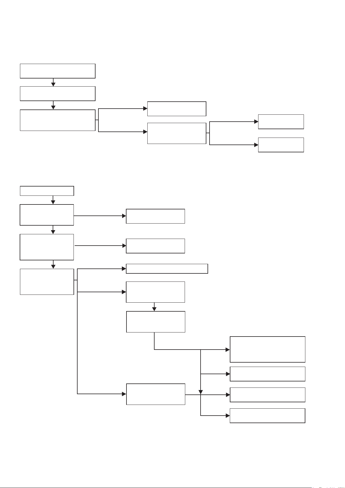
DISASSEMBLY
• Disassemble in order of the arrow in the following gure.
• In the case of the re-assembling, assemble it in order of the reverse of the following ow.
• In the case of the re-assembling, observe "attention of assembling".
• If wire bundles are untied or moved to perform adjustment or replace parts etc., be sure to rearrange them neatly as
they were originally bundled or placed afterward.
Otherwise, incorrect arrangement can be a cause of noise generation.
TOP COVER
FRONT PANEL ASSY
Refer to "DISASSEMBLY
1. FRONT PANEL ASSY"
and "EXPLODED VIEW"
POWER SW PWB UNIT
(Ref. No. of EXPLODED VIEW : 14)
HEADPHONE PWB UNIT
(Ref. No. of EXPLODED VIEW : 15)
FRONT PWB UNIT
(Ref. No. of EXPLODED VIEW : 18)
MAIN & VOLUME PWB UNIT
Refer to "DISASSEMBLY
2. MAIN & VOLUME PWB UNIT"
and "EXPLODED VIEW"
VOLUME PWB UNIT
(Ref. No. of EXPLODED VIEW : 19)
MAIN PWB ASSY
(Ref. No. of EXPLODED VIEW : 25)
POWER TRANS
Refer to "DISASSEMBLY
3. POWER TRANS"
and "EXPLODED VIEW"
POWER TRANS
(Ref. No. of EXPLODED VIEW : 27)
SUB TRANS
Refer to "DISASSEMBLY
4. SUB TRANS"
and "EXPLODED VIEW"
STANDBY PWB UNIT
(Ref. No. of EXPLODED VIEW : 29)
8
Page 9

About the photos used for "descriptions of the DISASSEMBLY" section
• The shooting direction of each photograph used herein is indicated on the left side of the respective photograph as
"Shooting direction: ***".
• Refer to the diagram below about the shooting direction of each photograph.
• Photographs with no shooting direction indicated were taken from the top of the set.
The viewpoint of each photograph
(Shooting direction)
Shooting direction: B
[View from the top]
1. FRONT PANEL ASSY
Front side
Shooting direction: DShooting direction: C
Shooting direction: A
Proceeding :
(1) Remove the screws.
View from bottom
View from top
TOP COVER
FRONT PANEL ASSY
→
9
Page 10

(2) Remove the screws.
Shooting direction: C
(3) Cut the wire clamp band.
Shooting direction: D
cut
cut
cut
10
Page 11

(4) Disconnect the connector wire. Remove the screws.
N8101
N8001
N3001
N7501
N6001
N3002
N8504
N8502
Please refer to "EXPLODED VIEW" for the disassembly method of each PWB included in FRONT PANEL ASSY.
11
Page 12

2. MAIN & VOLUME PWB UNIT
Proceeding :
(1) Detach the KNOB AL CAP POINTER. Remove the screws.
Shooting direction: B
(2) Remove the screws.
TOP COVER
MAIN & VOLUME PWB UNIT
→
Shooting of photograph: A
(3) Cut the wire clamp band, then disconnect the connector wire. Remove the screws.
N6001
N8101
N8001
N3001
N7501
N3002
cut
12
Page 13

3. POWER TRANS
Proceeding :
(1) Cut the wire clamp band, then disconnect the connector wire. Remove the screws.
N8101
N8001
TOP COVER
cut
POWER TRANS
→
cut
N8503
4. SUB TRANS
Proceeding :
(1) Remove the screws.
Shooting of photograph: A
(2) Disconnect the connector wire. Remove the screws.
TOP COVER
SUB TRANS
→
N8504
U model only
N8503
N8502
N8501
13
Page 14

WHEN THE MICROPROCESSOR IS REPLACED WITH A NEW ONE
When the U-PRO (Microprocessor) or the Flash ROM is replaced, conrm the following.
PWB Name Ref. No. Description
FRONT U1001 TMP86FH47UG C
After replacing
A : Mask ROM (With software). No need for write-in of software to the microprocessor.
B : Flash ROM (With software). Usually, no need for write-in of software. But, when the software was updated, you should
write the new software on the microprocessor or ash ROM. Please check the software version.
C : Empty Flash ROM (Without software). You should write the software on the microprocessor or ash ROM.
Refer to "Update procedure" or "writing procedure", when you write the software.
Necessary Equipment
• Windows PC (OS: Windows 2000 or Windows XP) with Serial port.
• RS-232C Cable straight type (9 Pin female - 9 Pin female)
• Connection JIG (90M-PM11S1JIG)
• Writing Tool and some les (FlashProg.exe, etc... in TM86FH47pass folder)
• Writing data (PM6004_xxxx.h16)
WRITING PROCEDURE
(1) Disconnect the mains cord from the unit.
(2) Connect RS-232C on the connection JIG and Serial Port of windows PC with RS-232C cable.
(3) Connect FPC (upside contact) to the rear panel of the unit from connection JIG.
After
replaced
Remark
(4) Reconnect the mains cord to the unit.
(5) Put the “TM86FH47pass” folder into anywhere on your PC’s hard disc.
14
Page 15

(6) Double click the TM86FH47pass folder.
(7) Double click FlashProg.exe.
15
Page 16

(8) Click Device tab.
(9) Click Apply.
16
Page 17

(10) TMP86FH47 appear in Chosen Device.
(11) Click Object File, and click Browse...
17
Page 18

(12) Choose iHEX Fomat[*.h16,*.h20] in Files of type.
Choose writing data, and click Open.
PM6004_V06.h16
(13) Click Communication tab.
PM6004
18
Page 19

(14) Choose COM port number in COM port.
Choose 9600 in Data Rate.
Click OK.
(15) When Setup window is closed, the tmp folder and FlashProg.ini le are created simultaneously.
Click Yes.
NOTE : These are the original set-up conguration les for that PC. They do not operate, if these les moved to
another PC. When you make it operate with other PC, delete the tmp folder and the FlashProg.ini le and
redo a setup.
19
Page 20

(16) The Flash Programmer is launched.
Click setup icon.
(17) Click Browse....
20
Page 21

(18) Choose FlashProg.ini in TM86FH47pass folder, and click Open.
(19) Click OK.
PM6004
21
Page 22

(20) Press the POWER ON/OFF button, and turn on the unit.
Status indication at lower left in Flash Programming window is changed to "Connected" from "Connecting".
When it did not changed, check the connection of FPC or RS-232C cable.
(21) Select Password in Setup.
22
Page 23

(22) Setup Password opens.
· When writing in a blank microprocessor (Refer to next page).
· When writing (update) in the already written-in microprocessor (Refer to 25 page).
23
Page 24

When writing in a blank microprocessor
Check Single Boot Mode in Address Mode.
Setting in Device Password
· Check Device is BLANK.
· Check Hex in input type.
· Since they are inputted automatically, please do not change text box of "Password", "Password Character Number
Address" and “Password Compare Start Address”.
Setting in Object File Password
· Do not check BLANK password.
· Check Hex in Input Type.
· Type 0102030405060708 into Password.
· Type 0xFF00 into Password Character Number Address.
· Type 0xFF01 into Password Compare Start Address.
Click OK.
24
Page 25

When writing in the already written-in microcomputer (update)
Check Single Boot Mode in Address Mode.
Setting in Device Password
· Check Device is BLANK.
· Check Hex in input type.
· Type 0102030405060708 into Password.
· Type 0xFF00 into Password Character Number Address.
· Type 0xFF01 into Password Compare Start Address.
Setting in Object File Password
· Do not check BLANK password.
· Check Hex in Input Type.
· Type 0102030405060708 into Password.
· Type 0xFF00 into Password Character Number Address.
· Type 0xFF01 into Password Compare Start Address.
Click OK.
25
Page 26

(23) Auto Programming opens.
26
Page 27

(24) Check All Erase, Programming, Verify with SUM and File Compare in Flash Memory Programming.
Check Manual in Recover Process by Programming Error.
Click Start.
27
Page 28

(25) Writing data is written into the microprocessor (U1001).
(26) Click Yes, when writing is successful.
28
Page 29

(27) Click Cancel.
(28) Click Cancel.
29
Page 30

(29) Select the Exit in File, and nish.
(30) Press the POWER ON/OFF button, and turn off the unit.
Disconnect each cable.
(31) Check the software version.
Refer to 31 "SERVICE MODE".
30
Page 31

SERVICE MODE
Microprocessor (U1001) version chseck
(1) Press the POWER button with pressing the SOURCE DIRECT button on the unit.
(2) The rmware version is displayed on the front LED. (Display time is only for 3 seconds.)
CDPHONO TUNER
Version : 16 8 4 2 1
The rmware version is displayed in the lighting position of LED.
Ex. :
Light up RECORDER-2 [1 ], Version : 1
Light up RECORDER-2 [1 ] and AUX/DVD [4 ], Version : 5
Light up RECORDER-2 [1 ] and CD [8 ], Version : 9
(3) Each LED light up then all LED light up.
(4) Turn off the power to quit Service Mode. (The unit to the default status)
RECORDER
MUTE1AUX/DVD 2
31
Page 32

ADJUSTMENT
IDLING CURRENT ALIGNMENT
Adjusting Procedure
Set the power voltage to rated voltage for this adjustment.
(1) Adjust the Idling Current with the variable resistor V6001 and V6002 on the PWB 8U-110004-1.
(2) Turn off the power.
(3) "+" of Connect Digital Voltage is connected to the No. 1 pin and connected "-" to No. 3 pin of N6003.
(4) "+" of Connect Digital Voltage is connected to the No. 1 pin and connected "-" to No. 3 pin of N6004.
(5) Before turning on the power, V6001 and V6002 have been counter clockwise turned with the adjustment driver.
(6) Turn on the power, VOLUME is set as -∞.
(7) After 2 minutes.
With seeing the digital voltage meter turn the variable resister clockwise slowly to adjust the idling current.
Idling adjustment with V6001 (V6002).
•Turn V6001 (V6002) clockwise to increase the idling current.
•The adjustment value of idling current is 10 mV(22.5 mA) ± 0.5 mV(1.1 mA) each.
(8) After 6 minutes.
Repeat the same procedure as 7.
•The adjustment value of idling current is 20 mV(45 mA) ± 0.5 mV(1.1 mA) each.
Adjustment is completed.
(9) Remove connection cable, attach the top cover.
NOTE : Idling current decreases with the temperature rise inside the unit, and it is set to 20 mV (45 mA) of setting value in
about 30 minutes after turn on the power.
32
Page 33

DC OFFSET VOLTAGE ADJUSTMENT
Digital Voltmeter Digital Voltmeter
V
R ch
N6003 V6001
V
L ch
V6003 V6004
N6004
V6002
Adjusting Procedure
DC Offset Voltage Adjustment
(1) Before turning on the power, Insert Digital Voltage Meter between the SPEAKERS SYSTEM A (L CH) "+" and "-".
Insert Digital Voltage Meter between the SPEAKERS SYSTEM A (R CH) "+" and "-".
(2) Adjust the VOLUME to MIN.
(3) Turn on the power. Then turn the SPAKERS SW to A.
Adjustment is started immediately after a speaker relay turns on.
(4) First L CH is adjusted.
The variable resistor V6003 on 8U-110004-1 is turned with adjustment driver, and the Digital Voltage Meter is
adjusted to "0 mV ± 3 mV".
(5) Then, R CH is adjusted.
The variable resistor V6004 on 8U-110004-1 is turned with adjustment driver, and the Digital Voltage Meter is
adjusted to "0 mV ± 3 mV".
NOTE : DC offset voltage drops when turn the semi-xed resistor (V6003 and V6004) clockwise. DC offset voltage rises
when turn the semi-xed resistor un-clockwise. Please turn it slowly, because value of Digital Voltage Meter
changes slowly.
(6) Although after-adjustment DC offset voltage has some change, Please check that the range of DC offset voltage
between L ch (R ch) "+" and L ch (R ch) "-" terminal of SPEAKERS SYSTEM A is "0 mV ± 20 mV". CHART OF
FACTORY MODE.
33
Page 34
TROUBLE SHOOTING
1. The power can not be turned on.
(STANDBY LED does not light (STANDBY MODE)
Checkinsertion of the 8U110005-3 STANDBY PWB UNIT.
Check insertion of the 8U110005-1 FRONT PWB UNIT.
Power not supplied.
Check whether power is being
supplied to the coil of the SUB
TRANS T8501.
Power supplied.
2. The power can not be turned on. (STANDBY LED lights→ash)
Check each connector.
Broken wire in SUB
TRANS T8501
Check whether power
is being supplied to the
D8501-8506
.
.
Power not supplied.
Power supplied.
Malfunction of
D8501-8506
Malfunction of
U8501,U1001.
Check whether power
is being supplied to
the F8510
Check whether power
is being supplied to
the coil of the POWER
TRANS T0001
Check whether power
is being supplied to
the D8001,D81018104,D8201-8202
.
.
Power not supplied.
Power not supplied.
Power not supplied.
Power supplied.
<*1>
Broken wire in STANDBY
F8510
.
Broken wire in POWER
TRANS T0001
Broken D8001,D8101-8104,D8201-8202
STANDBY LED repeats
ON/OFF for 0.5 seconds
each.
Check input level, SPEAKER
connection and SPEAKER
resistance value.
.
.
Damaged DC OFFSET DETECT.
Damaged OVER HEAT DETECT.
Damaged OVER CURRENT
DETECT.
Damaged P_DWN detection
circuit and U1001.
Power supplied.
<*2>
STANDBY LED repeats
ON/OFF for 0.25
seconds each.
34
Damaged power amplier circuit
Damaged power circuit.
Page 35

3. STANDBY LED ashes while using unit. (protection circuit is set)
Check each connector
Refer to <*1><*2> in "The power can not be
turned on. (STANDBY LED lights→ash)"
4. The power turned on, but a sound does not output normally. (Both channels)
4.1 STANDBY LED does not ash (protection mode is not set)
Check each connector
Check whether power is being
supplied to the coil of the
POWER TRANS T0001
4.2 When the volume is turned up, Mute LED ashes. (protection mode is set)
Repeats ON/OFF for 0.5 second each, and automatically returns to normal operation.
Check input level and
each connector
Check SPEAKER connection
and SPEAKER short,
SPEAKER resistance value.
Power not supplied.
Power supplied.
Power supplied.
Broken wire in POWER TRANS
T0001
.
Damaged Selector (U3501)
Mute Circuit (Q6001-6002,L7501-7502).
Damaged Mute circuit, U1001.
When you turn up the volume again after the unit
automatically returns to normal operation and if
the protection circuit is activated, STANDBY LED
will repeat ON/OFF for 0.25 seconds each.
Damaged power amplier
circuit
Malfunction of C7501-7504
35
Page 36

Personal notes:
36
Page 37

BLOCK DIAGRAM
PHONO BLOCK
PHONO AMP
PHONO
PM6004 BLOCK DIAGRAM
TUNER
CD
AUX / DVD
RECORDER-1
IN
RECORDER-2
IN
RECORDER-1
OUT
RIAA
REC OUT SELECTOR
INPUT SERECTOR
REC BUFFER
LOUDNESS
BLOCK
ON
OFF
LOUDNESS
LINE DETECT
PRE AMP BLOCK
VOLUME
M
PRE AMP
NFB
TONE AMP BLOCK
TONE AMP
TREBLE
SOURCE DIRECT
BASS
ON
OFF
BALANCE
MUTE
POWER AMP BLOCK
POWER AMP
NFB
PROTECTION
SPEAKER
RELAY
SPEAKER
RELAY
HEADPHONE
RELAY
SPEAKER-A
(+)
SPEAKER-A
(-)
SPEAKER-B
(+)
SPEAKER-B
(-)
HEADPHONE
RECORDER-2
OUT
REGULATOR BLOCK
USA VERSION ONLY
AC OUTLET
AC IN
FUSE
FUSE
INPUT BLOCK
STANDBY
RELAY
POWER SW
FUSE
LINE DETECT
AMP
MAIN TRANS.
SUB TRANS.
±38V
PROTECTION
±15V
+12V
+5V
+5V
P_OFF DETECT
POWER AMP
PRE AMP
FUNCTION RELAY
FUNCTION LED
MCU
U-COM BLOCK
POWER DETECT
LINE DETECT
PROTECTION
FRONT SW FUNCTION LED
EEPROM
I/R SENSOR
FLASHER IN
USA VERSION ONLY
MCU MOTOR DRIVER
RC5
FLASHER
RELAY DRIVER
MUTE
INPUT SELECTOR
RC5 IN/OUT
37
Page 38

POWER SUPPLY BLOCK DIAGRAM
AC OUTLET
USA VERSION ONLY
K8601
F8610
FUSE
FUSE
AC INLET
J0001
S8501
STANDBY
RELAY
F8510F8620
FUSE
T0001
MAIN
TRANS.
D8001
C8001
A_GND
D8101-D8104
C8101
C8102
D8201
D8202
C8201 C8202 C8203
C8002
PM6004 POWER SUPPLY DIAGRAM
+38V
-38V
U8101
+15V
+15V
C8103
C8104
-15V
-15V
U8102
+12V
U8201 U8202
+12V
+5V
+5V
POWER AMP
PHONO AMP
INPUT SELECTOR, REC BUFFER,
LINE DETECTOR.
PRE AMP
TONE AMP
A_GND
SP RELAY, HP RELAY
SOURDE DIRECT, LOUDNESS RELAY
MOTOR VOLUME DRIVER
FUNCTION LED
S8901 T8501
POWER SW
SUB
TRANS.
D8501-D8504
D_GND
D8505
U8501
C8504 C8506
C8503
D_GND
D8506
+9V
+5V
D_GND
STANDBY RELAY
+5V
MCU, EEPROM, I/R RECEIVER
STANDBY LED, INPUT SELECTOR SW,
FUNCTION SW
+9V
P_OFF DETECTOR
D_GND
FLASHER IN (USA VERSION ONLY)
38
Page 39

LEVEL DIAGRAM
[dB] [dB]
+30
SP out:45W/8Ω +25.56dB(18.97V)
+30
+20
+10
0
-10
-20
-30
-40
-50
-60
PHONO
CD:-13.97dB(200mV)
Phono Amp Gv=39.2dB
MM:-53.15dB(2.2mV)
PHONO AMP
Power Amp Gv=24.1dB
+1.43dB
Pre Amp Gv=15.4dB
-13.97dB
Input Block Pre Amp Block Tone Amp Block Power Amp Block
+20
+10
0
-10
-20
-30
-40
-50
-60
TUNER
CD
AUX / DVD
RECORDER-1
IN
RECORDER-2
IN
RECORDER-1
OUT
RIAA
REC OUT SELECTOR
INPUT SERECTOR
REC BUFFER
LOUDNESS
LINE DETECT
VOLUME
M
PRE AMP
NFB
TONE AMP
TREBLE
BASS
SOURCE DIRECT
BALANCE
MUTE
POWER AMP
NFB
PROTECTION
SPEAKER
RELAY
SPEAKER
RELAY
HEADPHONE
RELAY
SPEAKER-A
(+)
SPEAKER-A
(-)
SPEAKER-B
(+)
SPEAKER-B
(-)
HEADPHONE
RECORDER-2
OUT
LINE DETECT
AMP
39
Page 40

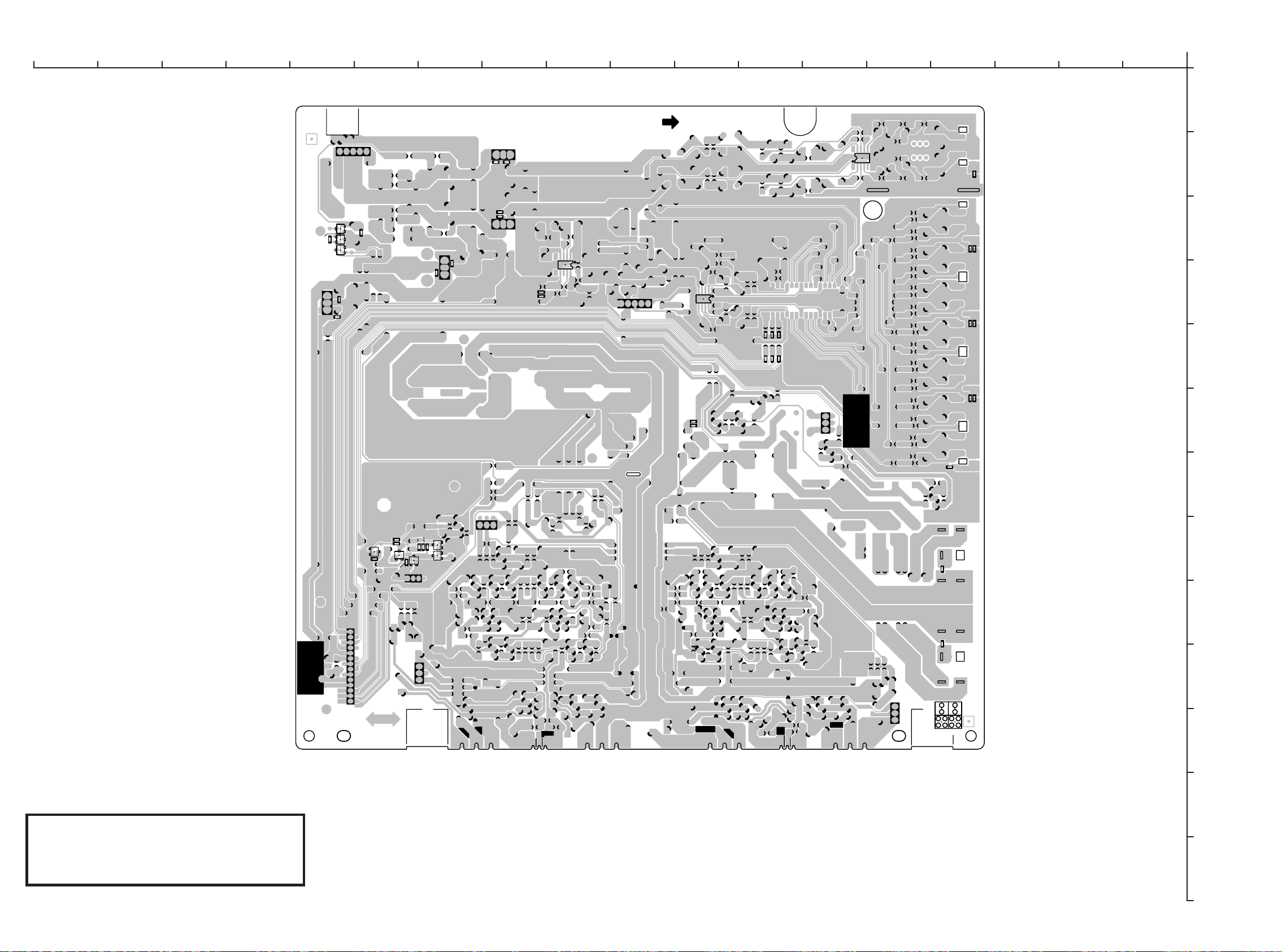
PRINTED WIRING BOARDS
FRONT
(COMPONENT SIDE)
181716151413121110987654321
A
9
Z1603
9:TXD
Z1601
JV1079
JV1052
JV1036
JV1011
JV1060
JV1061
6:P_RELAY
7:ICE4
8:RXD
B1001
15.0
15.0
12.5
1:RC5
2:P_ON
3:D_GND
4:+5VL
5:P_DOWN
12.5
J2001
1
JV1016
JV1048
7.5
7.5
D1501
7.5
JV1037
JV1049
JV1001
JV1006
JV1017
7.5
7.5
STANDBY
7.5
JV1065
JV1044
7.5
7.5
7.5
7.5
JV1045
JV1007
7.5
15.0
JV1066
JV1053
JV1031
12.5
20.0
JV1018
12.5
7.5
JV1026
JV1012
7.5
JV1008
7.5
JV1019
S1411
B1005
C1001
JV1020
7.5
JV1054
JV1073
JV1062
JV1032
JV1057
JV1072
JV1080
X1001
17.5
25.0
B1004
12.5
12.5
15.0
25.0
C2017
R2015
C2011
JV1033
JV1021
R2019
C2015
R2017
R2013
JV1002
JV1027
7.5
JV1067
25.0
JV1081
JV1005
7.5
15.0
JV1058
C2013
1
JV1087
JV1074
JV1038
V2003
BASS
7.5
7.5
JV1050
D1502
PHONO
12.5
7.5
SOURCE
DIRECT
JV1028
JV1003
12.5
D1509
S1401
C2012
JV1014
7
JV1022
JV1034
7.5
JV1046
JV1023
7.5
7.5
JV1055
C2018
D1503
TUNER
JV1047
12.5
JV1039
JV1013
JV1082
C2014
7.5
C2016
R2020
R2016
7.5
JV1063
SPK A
S1403
R2014
R2018
1
CD
1:CE
2:DATA
3:CLK
JV1083
JV1075
JV1035
4:+5VD
5:D-GND
6:F_MUTE
22.5
17.5
JV1068
JV1040
B1002
AUX/DVD
7:A_MUTE
8:PROT_1
9:P_RALAY
10:+12V
11:PROT_2
R2005
R2003
JV1059
17.5
TREBLE
D1504 D1505
D1510
JV1024
22.5
JV1041
LOUDNESS
C2005
C2006
15.0
R1801
REC2/MD/TAPE
D1512
S1402
C2007
C2009
R2009
JV1070
JV1056
C2008
JV1004
R2010
R2012
R2008
14
D1506 D1507
REC1/CD-R
JV1085
JV1009
15.0
12:SPK_A
13:SPK_B
14:DET
D1511
7.5
7.5
SPK B
S1404
7.5
C2003
R2007
C2004
JV1069
JV1076
JV1029
R2004
R2006
JV1084
V2002
7 7
D1801
JV1077
C2010
12.5
JV1064
JV1010
11
1
D1508
MUTE
12.5
12.5
12.5
JV1051
7.5
R2011
BALANCE
B1006
JV1030
7
5
6:NC
7:NC
C2002
12.5
V2001
1:+12V
Q1803
JV1025
C1801
3:TO_L
4:A_GND
5:TO_R
12.5
N1002
C2001
JV1042
2:LOUD
3:MOT+
4:MOT-
1:+15V
2:-15V
5:D-GND
B
E
C
7.5
B
C
Q1802
C2020
JV1078
1
R2002
R2001
JV1015
E
JV1
1
E
C
Q1804
JV1086
R2022
B1003
B
7.5
17.5
R2021
E
C
Q1801
S2001
3
B
7.5
JV1071
C2019
D2001
63101000510AM
8U-110005-1
D1601
FRONT UNIT
1:L
2:A_GND
3:R
C1603
JV1043
U1601
C1601
G
OUT
VCC
B
C
1
D
E
F
FRONT
(FOIL SIDE)
C1604
R1601
R1602
C1602
Q1603
Q1602
Q1601
3
R1605
Q2001
R1603
1
R1804
R1802
Q1604
R1604
G
R1005
C1503
R1518
4
R1505
R1515
C1401
R1401
R1403
5
C1507
R1516
R1402
R1006
R1007
C1005
C1502
R1504
R1503
R1502
C1006
C1501
7
Q1004
R1017
1
R1016
C1002
Q1009
8
1
R1015
33
34
U1001
5
U2002
4
Q1005
C1010
23
44
Q1006
Q1007
22
1
Q1008
12
11
R1013
4
5
1
8
R1012
R1011
C1009
U1003
R1014
R1008
R1009
C1902
R1903
3
U1002
R1010
C1007
Q1003
R1004
C1004
R1001
C1003
1:RC5
2:P_ON
3:D_GND
R1902
Q1002
R1003
5:P_DOWN
6:P_RELAY
4:+5VL
9
R1901
8:RXD
9:TXD
7:ICE4
H
I
1
R1002
Q1010
1
54
C1008
C1412
C1411
R1411
R1412
R1501
Q1001
J
R1808
R1806
R1805
R1809
R1807
1:+15V
3:TO_L
2:-15V
1
3
1
1:L
2:A_GND
3:R
5
R1803
4:A_GND
5:TO_R
6:NC
7:NC
1
1:+12V
2:LOUD
3:MOT+
4:MOT-
5:D-GND
R1513
R1514
R1512
7
7
1
R1521
1
R1522
C1510
8 5
U2001
4
R1511
C1506
R1519
C1509
14
R1520
R1510
C1505
R1509
R1406
7
14:DET
13:SPK_B
11:PROT_2
12:SPK_A
R1405
R1404
R1507
C1504
R1508
10:+12V
9:P_RALAY
7:A_MUTE
8:PROT_1
1
1
3:CLK
4:+5VD
5:D-GND
6:F_MUTE
C1508
R1517
U2003
1:CE
2:DATA
8
1
R1506
K
鉛フリー半田
半田付けには、鉛フリー半田 (Sn-Ag-Cu) を使用してください。
Lead-free Solder
When soldering, use the Lead-free Solder (Sn-Ag-Cu).
L
M
40
Page 41

181716151413121110987654321
VOLUME
(COMPONENT SIDE)
R5038
R5040
R5037
R5039
JV5001
C5010
JV5007
C5009
B
C
E
B
C
E
R5034
Q5013 Q5014
Q5015
R5033
R5035 R5036
C5008
B
C
E
R5046
C5007
B
C
E
R5045
R5032
Q5016
R5030
C5006
R5031
R5029
C5005
N5002
7
D5006
R5024
12.5
R5023
12.5
R5027 R5028
B
C
E
D5005
B
C
E
R5043
B
C
E
R5022
Q5012
R5044
B
C
E
R5021
R5025 R5026
Q5011
4.A_GND
5.TO_R
R5020
Q5010
JV5012
R5042
R5019
Q5009
D5003 D5004
JV5011
2.-15V
3.TO_L
D5002
R5016
D5001
R5015
R5017 R5018
R5041
1.+15V
1
B
C
E
B
C
E
B
C
E
B
C
E
Q5006Q5007 Q5008
JV5004
Q5005
JV5005
Z5001
R5012
15.0
R5011
15.0
R5010
R5007 R5008
R5013 R5014
R5009
B
C
E
B
C
E
R5004
C5002
JV5008
JV5021
JV5002
B
C
E
B
C
E
R5003
C5001
JV5014
Q5002
Q5001
R5005 R5006
Q5003 Q5004
JV5013
JV5024
C5004
JV5009
7.5
7.5
JV5006
JV5016
12.5
7.5
JV5023
C5003
7.5
7.5
R5047 R5048
C5012
B5002
C5011
V5001
1.+15V
2.-15V
JV5003
7.5
3.IN_L
4.A_GND
1
B5001
5.IN_R
5
8U-110005-2
VOLUME UNIT
JV5017
7.5
JV5018
C2504
R2502
7.5
R5002
R5001
1
C2505
D2501
S2501
C2502
1
7.5
JV5020
N5001
1.+12V
2.LOUD
3.MOT+
C2501
5
4.MOT-
5.D_GND
R2503R2504
R2501
C2503
STANDBY
(COMPONENT SIDE)
R
B8502
L
K8701
JV8512
Z8701
D8702
JV8511
C8701
G
VCC
OUT
K8501
1
2 4
B8501
JV8502
JV8501
Q8501
E
B
C
D8508
1
S8501
3
U8701
Japan/USA: T3.15AL 250V
D8701
Europe/China: T1.6AL 250V
(Sec.)
JV8500
2
C8502
4
F8510
H8512
H8511
(Pri.)
C8506
4
2
17.5
JV8509
F8620
T5.0AL 250V
N8503
4.+5VL
5.P_DOWN
6.P_RELAY
7.ICE4
8.RXD
9.TXD
R8501
C8504
D8507
T8501
JV8504
1
N8501
1
T5.0AL 250V
K8601
1
23
1
JV8510
22.5
1.RC5
2.P_ON
3.D_GND
5 9
F8610
7.5
JV8503
JV8505
2
9
N8504
JV8507
15.0
7.5
7.5
D8505
C8503
D8502
D8503
D8504
1
15.0
D8501
JV8506
D8506
2
N8502
1
JV8514
JV5813
2 4
1
4.RXD
5.ICE4
8U-110005-3
STANDBY UNIT
JV8508
15
5
2.D_GND
1.+5VL
3.TXD
Z8502
1
Z8501
N8505
(Sec.)
(Pri.)
A
B
C
D
E
F
VOLUME
(FOIL SIDE)
1
5
1.+12V
2.LOUD
3.MOT+
4.MOT-
5.D_GND
Q2501
鉛フリー半田
半田付けには、鉛フリー半田 (Sn-Ag-Cu) を使用してください。
2.-15V
3.IN_L
4.A_GND
5.IN_R
5
C5013
8 7 43 216 5
1.+15V
1
1.+15V
2.-15V
3.TO_L
1
4.A_GND
5.TO_R
STANDBY
G
(FOIL SIDE)
9
Q8503
4
5
4.RXD
3.TXD
C8509
5.ICE4
2
1
2
1
2.D_GND
1.+5VL
7
R8503
1
1
(Sec.)
(Pri.)
2 3
2
1
8.RXD
9.TXD
1
3.D_GND
4.+5VL
5.P_DOWN
6.P_RELAY
7.ICE4
678 59
1
2
1.RC5
2.P_ON
U8501
I
C8510
4
2
3
H
G
O
D8509
C8505
R8505
Q8502
R8502
I
2
4
1
3
R8702
Q8701
C8702
J
K
R8701
C8508
R8504
C8507
2
1
4
3
R
L
L
Lead-free Solder
When soldering, use the Lead-free Solder (Sn-Ag-Cu).
M
41
Page 42

181716151413121110987654321
POWER SW
(COMPONENT SIDE)
(Pri.)
1
8U-110005-4
POWER SW
S8901
B8901
2
1
C8901
POSISTER
(COMPONENT SIDE)
POWER SW
(FOIL SIDE)
(Pri.)
POSISTER
(FOIL SIDE)
HEADPHONE
(COMPONENT SIDE)
K9901
Z9901
8U-110005-5
C9901
C9902
H/P UNIT
1
R9901
R9902
3
B9901
1
3.HP_R
2.NC
1.HP_L
2
1
HEADPHONE
(FOIL SIDE)
3
3.HP_R
2.NC
1.HP_L
1
A
B
C
D
E
F
B6501
8U-110005-6
T6501
1
3
1
G
H
I
J
K
鉛フリー半田
半田付けには、鉛フリー半田 (Sn-Ag-Cu) を使用してください。
Lead-free Solder
When soldering, use the Lead-free Solder (Sn-Ag-Cu).
L
M
42
Page 43

MAIN
(COMPONENT SIDE)
K4001
K3001
K3004
K7501
LOWLOW
UP
UP
LOW
UP
LOW
UP
LOWLOW
UP
UP
MPMP
C4002
C4001
C3010
K3002
K3003
R7505
R7506
7.5
JV46
MKMK
B
C
E
R4002
R4001
Q7504
C7502
12.5
R3002
C3009
R3003
C3012
C3011
C3014
R3012
C3013
C3016
R3016
C3015
C3018
R3020
C3017
R3019
C3020
R3024
C3019
R3023
C3022
R3028
C3021
R3027
S7502
D7502
JV11
L4002
R4005
L4001
R3009
R3011
R3015
C7504
C7503
12.5
R4006
R4004
R4003
R3004
R3001
R3006
R3008
R3005
R3007
R3010
JV189
R3014
R3013
R3018
R3017
R3022
R3021
R3026
R3025
22.5
JV146
R9003
N6003
C4004
C4003
JV53
JV144
7.5
JV93
JV151
JV188
25.0
25.0
JV137
JV154
22.5
C7501
Q9001
R4008
R4007
JV31
JV127
JV29
JV180
JV28
JV69
B
JV19
15.0
17.5
17.5
17.5
17.5
15.0
JV158
15.0
S7501
JV96
JV192
JV167
22.5
R9005
C
25.0
JV89
25.0
JV159
JV16
22.5
R9007
D9001
E
R6093
R9001
C4006
R4010
JV13
C4005
R4009
Z4001
25.0
D7501
E
22.5
17.5
25.0
JV94
3.HP_R
2.NC
1.HP_L
JV179
7.5
JV49
C6011
JV183
17.5
Q6131
C
C4008
C4007
17.5
JV105
R7503
JV112
R6105
Q6111
B
E
B
12.5
B
C
E
Q7503
JV5
U3501
N7501
C6024
C6007
D6005
R6035
R6031
R6083
B
C
E
R6089
JV191
C6022
C6023
C6021
Q6033
R6087
R6069
C4010
R4012
C4009
R4011
JV38
JV109
JV2
JV190
R7504
R6106
R6023
R6057
R6043
R6073
R6077
R6067
Q6031
R3505
D3501
R6019
Q6015
B
C
E
Q6023
B E
C4013
R7508
J6002
D6001
B
C
E
Q6011
B
C
E
R6053
R6081
C4014
7.5
JV54
R7507
B
C
E
JV136
R4014
C4011
JV163
JV40
S7503
B
C
E
Q6007
Q6019
15.0
Q6027
V6001
C4012
R4013
JV62
Q7505
JV98
E
C
B
C6015
JV181
JV135
R6071
R4016
JV141
E
C6003
R6015
Q6003
7.5
R6047
R4015
C3506
B
C
E
R6051
R6079
JV125
22.5
R3502
R3503
R3501
D7503
J6001
R6097
R6039
R6049
JV160
22.5
B
C
E
C3502
R3504
17.5
Q7501
B
C
E
L6002
L6001
R6009
R6011
R6029
C6017
R6041
12.5
C6019
JV86
Q6035
E
C4016
C4018
C4017
C4015
JV78
C3802
22.5
C3501
JV55
JV140
R7501
R9010
JV170
Q6005
JV194
JV85
R6085
Q6132
R3901
R3902
R3802
R7502
7.5
R9009
C6001
R6027
B
C
E
R6099
Q6021
D6007
R6061
Q6029
7.5
7.5
Q6112
C
R3804
R3803
R3801
E
JV47
B
C
E
R6017
B
C
E
B
C
E
B
E
R4018
R4017
JV68
7.5
Q7502
Q6001
B
C
E
Q6009
Q6017
JV145
7.5
B
R4020
R4019
12.5
JV175
JV133
15.0
12.5
C3801
JV198
7.5
25.0
R6005
D6003
Q6013
R6101
E
C
B
R6045
B
C
E
R6055
12.5
C4019
C4020
JV100
JV178
R6003
B
C
E
R6059
Q6025
R6095
JV73
JV7
JV76
C3901
JV193
JV110
22.5
R6001
R4021
R4022
25.0
JV107
JV174
JV67
R6007
R6033
R6037
7.5
JV51
R6075
JV30
R6091
20.0
JV130
JV4
JV81
7.5
JV41
C6013
JV161
15.0
JV115
17.5
25.0
15.0
JV185
C6009
R6021
R6025
R6103
R6109
JV173
DIP
258X241
JV172
17.5
15.0
JV121
JV116
25.0
22.5
25.0
20.0
C3804
JV168
JV164
15.0
20.0
7.5
JV195
20.0
15.0
7.5
15.0
JV142
22.5
22.5
22.5
JV152
JV58
JV35
R6076
JV99
25.0
C3803
JV120
12.5
JV8
JV70
JV15
JV186
JV87
7.5
12.5
7.5
JV6
7.5
JV20
R6096
15.0
JV42
25.0
JV103
R3806
JV92
JV139
JV108
E
JV39
N3001
5.R
4.A_GND
B8001
12.5
JV34
V6003
JV22
JV60
JV23
C6010
R6022
R6110
R6034
JV77
C6014
Q6142
R3805
C8002
R6066
C
2.-15V
1.+15V
3.L
Z4007
R6026
R6104
D6008
Q6122
C3903
R3904
JV18
C3906
R3905
C8001
R6063
R6046
B
C
E
R6060
B
E
R6092
B
IM
15.0
22.5
JV33
JV48
15.0
JV169
D6009
D6011
JV155
Q6014
B
C
E
JV1
R6038
B
C
E
Q6030
R6056
Q6026
R6086
B
C
E
JV118
D3901
R3906
C3904
15.0
17.5
D6004
Q6010
Q6018
B
7.5
C
E
Q6036
R6082
R6080
R6068
D3903
15.0
JV124
D6010
17.5
JV88
B
C
E
R6102
Q6022
JV43
R6062
12.5
Q6032
C3902
R3903
D3902
JV10
D6012
C6004
R6018
JV80
E
C
B
C6020
7.5
JV50
7.5
7.5
12.5
R6070
15.0
B E
V6004
B
C
E
R6100
C6018
D8106
C3907
JV129
7.5
R6064
R6012
Q6006
R6050
JV52
JV37
JV75
B
C
R6088
R6078
R6072
D8105
R6010
R6028
JV32
R6042
R6052
E
JV111
20.0
R6065
JV12
C6002
Q6004
R6030
R6098
R6040
R6048
R6084
Q6034
V6002
1
U8101
O
G
I
O
U8102
J6003
7.5
I
C8103
C8104
G
JV36
12.5
JV24
JV71
12.5
C8201
JV150
D8001
7.5
C8102
JV131
Z4004
C8101
R8002
R9105
I
G
O
U8201
C8003
R8001
R9104
15.0
JV65
63101000410AM
JV61
R9102
R6008
B
C
E
B
C
E
JV44
8U-110004
R9103
R9101
N6001
R6108
Q6002
B
C
E
R6016
Q6008
Q6020
B
C
E
C6016
Q6028
R6054
JV182
B
C
E
B
C
E
15.0
JV3
R6006
JV27
Q6016
Q6024
R6094
E
2.A_GND
1.L
R6002
D6002
Q6012
E
C
B
17.5
R6058
JV9
C
3.R
R6004
E
C
B
15.0
Q6121
Q6141
JV177
JV64
Z4003
B
C
E
C9003
C6012
7.5
7.5
7.5
B
E
B
R6044
Q9003
R6032
R6036
D6006
7.5
JV25
R9011
C6008
R6020
R6024
JV21
JV123
JV165
JV95
C9001
N9001
12
25.0
JV106
Z8201
JV66
7.5
Q9002
R6074
R9106
12.5
JV14
1
3.NC
D9002
12.5
JV196
1.HEAT
2.GND
R9008
R9004
R9002
D8104
D8102
JV199
D8103
D8101
N8001
JV72
R9006
B
C
N6004
D8201
D8202
15.0
JV17
JV45
20.0
E
14.DET
13.SPK_B
12.SPK_A
11.PROT_2
10.+12V
9.P_RELAY
8.PROT_1
7.A_MUTE
6.F_MUTE
5.D_GND
4.+5VD
3.CLK
R6090
JV56
15.0
17.5
17.5
JV83
JV57
7.5
JV26
C9004
12.5
2.DATA
1.CE
N8101
R8102
R8101
C9101
JV79
7.5
12.5
J6005
JV197
12.5
12.5
JV63
25.0
JV59
17.5
C8202
C8203
JV91
25.0
JV162
20.0
JV149
JV114
JV74
D6203
N3002
B8101
Z4005
I
G
O
Z4002
7.5
JV153
R6201
Z4006
181716151413121110987654321
A
B
C
D
U8202
J6004
E
F
G
H
I
J
K
鉛フリー半田
半田付けには、鉛フリー半田 (Sn-Ag-Cu) を使用してください。
Lead-free Solder
When soldering, use the Lead-free Solder (Sn-Ag-Cu).
L
M
43
Page 44
MAIN
(FOIL SIDE)
181716151413121110987654321
A
DIP
Q9103
Q9102
R9108
Q9101
C8207
C8206
R9107
C8205
C8204
C8105
C8108
C8106
C8107
R3907
C3905
U3901
U3801
R6013
C6005
C3505
C3504
R3507
R3508
C3503
R3506
U4001
C3007
C3001
C3003
C3006
B
C4021
C
C3002
D
C3004
E
C3005
F
Q9008
C9005
R9012
R9013
Q9007
R9014
R9015
C9002
Q9006
R9016
Q9004
Q9005
MK2
MP2
C7506
C7505
MKMK
MP1
G
H
I
J
MK1
MPMP
K
L
鉛フリー半田
半田付けには、鉛フリー半田 (Sn-Ag-Cu) を使用してください。
Lead-free Solder
When soldering, use the Lead-free Solder (Sn-Ag-Cu).
M
44
Page 45

L4001/L4002:N/K ONLY
87654321
R4001/R4002:N/K 6.8K
C4001/C4002:N/K ONLY
1
L
PHONO IN
K4001
R
L
TUNER IN
R
L
CD IN
R
K3001
L
AUX IN
R
L
REC1 IN
R
K3002
L
REC1 OUT
R
L
REC2 IN
R
K3003
L
REC2 OUT
R
K3004
MAIN PWB
8U-110004-1
3
2
C4021
1
2
3
4
5
6
1
2
3
4
5
6
1
2
3
4
5
6
1
2
3
220P
C4001
220P
C4002
0.1Z
C3009-C3022:N/K ONLY
0.1Z
C3001
0.1Z
C3002
0.1Z
C3003
0.1Z
C3004
0.1Z
C3005
0.1Z
C3006
0.1Z
C3007
R4001
6.8K
L4001
BALUN-TRANS
L4002
BALUN-TRANS
R4002
6.8K
220P
C3009
C3010
220P
C3011
C3012
220P
C3013
C3014
220P
C3015
C3016
220P
C3017
C3018
220P
C3019
C3020
220P
C3021
C3022
Z4001
OPEN
OPEN
U SHORT
220P
220P
220P
220P
220P
220P
220P
R3001
R3005
R3009
R3013
R3017
R3021
R3025
C4003
10/50
R4003
R4004
C4004
10/50
220K
220K
220K
220K
220K
220K
220K
330K
330K
220K
R3002
A_GND2
220K
R3006
220K
R3010
220K
R3014
220K
R3018
220K
R3022
220K
R3026
R4005
R4006
R4007
100
56K
56K
R4008
100
R3003
R3004
R3007
R3008
R3011
R3012
R3015
R3016
R3019
R3020
R3023
R3024
R3027
R3028
220
220
220
220
220
220
220
220
560
560
220
220
560
560
C4005
C4006
TU_L
TU_R
CD_L
CD_R
AUX_L
AUX_R
REC1_L
REC1_R
RO1_L
RO1_R
REC2_L
REC2_R
RO2_L
RO2_R
220P
220P
100
R4009
100
R4010
RO2_L
R3506
C4007
220/25
C4008
220/25
RO1_L
R3507
120
U4001
45
120
C4009
678
C4010
REC2_L
C3505
C3504
C3503
R3508
0.039
REC1_L
470P
470P
1000P
120
0.039
123
NJM2068MD
R4012
R4011
82K
AUX_L
82K
CLK
DATA
R4015
R4016
R4014
TU_L
CE
GND POWER + POWER -
R4013
100
100
C4020
C4019
6.8K
6.8K
CD_L
R3501
C3501
R4022
100/25
100/25
C4012
47
10/50
C4011
10
R4021
10
1000P
PH_L
1000P
C4014
R3503
C4013
0.01
LC78212-E
1
L1
2
L2
3
L3
4
LCOM1
5
L4
6
L5
7
l6
8
LCOM2
9
L7
L8
10
LCOM3
11
VEE
12
CE
13
DI
14
CL
15
100K
0.01
C4015
10/50
-15V
+15V
C4016
10/50
U3501
R4019
100
100K
OPEN
C4017
R4017
OPEN
100K
R4018
C4018
R4020
100
PH_R
CD_R
PH_R
TU_R
R1
30
R2
29
R3
28
RCOM1
27
R4
26
R5
25
R6
24
RCOM2
23
R7
22
R8
21
RCOM3
20
VDD
19
RES
18
S
17
VSS
16
R3505
10K
R3504
100K
D3501
1SS133
C3506
4.7/50
STBY POWER
PH_L
AUX_R
C3803
C3804
REC1_R
R3502
C3502
100/25
100/25
47
10/50
REC2_R
U3801
R3805
R3806
RO1_R
8
1
10
10
From Volume PWB B1003
R6001
10
R6002
10
RO2_R
7
6
4 5
3
2
AZ4580MTR
A_GND3R
N6001
1L2
3P-BASE
L_CH
R_CH
220K
R6003
220K
R6004
C3801
R3803
10/50
100K
R3801
100K
R3802
C3802
R3804
10/50
N3001
5P-BASE
From Front PWB B5001
R6108
1K
1K
1
+15V2-15V
R6005
330
R6007
1K
C6005
0.022Z
R6013
1M
R6006
330
R6008
1K
SHORT
KTC2874B
KTC2874B
4
3
L
A_GND
C6011
470/63
C6007
OPEN.
C6001
R6011
100
22/50
FAS
47K
100P
C6003
R6009
Q6001
C6009
OPEN.
C6013
470/63
-15V
C6012
470/63
C6008
OPEN.
C6002
R6012
100
22/50
47K
FAS
100P
C6004
R6010
Q6002
C6010
OPEN.
C6014
470/63
39K
OPEN
C3903
R3904
R3902
10K
R3901
10K
C3902
10/50
100
220P
C3901
R3903
C3907
+15V
-15V
5
R
L ch SIGINAL LINE
D6001
R6015
R6017
D6003
D6002
R6016
R6018
D6004
OPEN
SHORT
R6023
33K
Q6011
R6019
1SS133
22
Q6003
KTA1268GR
Q6005
KTC3200GR
22
1SS133
Q6013
33K
R6021
SHORT
R6025
SHORT
R6024
33K
Q6012
R6020
1SS133
22
Q6004
KTA1268GR
Q6006
KTC3200GR
22
1SS133
Q6014
33K
R6022
SHORT
R6026
C3906
OPEN
D3901
1SS133
U3901
1
8
2
7
3
6
45
AZ4580MTR
OPEN
C3905
KTC3200GR
Q6007
KTC3200GR
22
R6027
22
R6029
KTA1268GR
Q6009
KTA1268GR
R6097
100
KTC3200GR
Q6008
KTC3200GR
22
R6028
22
R6030
KTA1268GR
Q6010
KTA1268GR
R6098
100
D3903
1SS133
100K
R3907
D_GND2
C6015
C6016
47K
R3906
D3902
CLK
DATA
CE
14P-BASE
Q6015
FNS
330P
Q6017
R6099
330
Q6016
FNS
330P
Q6018
R6100
330
C3904
1SS133
N3002
470
R6031
KTA1268GR
1M
R6039
1M
R6041
KTC3200GR
470
R6033
R6101
330
470
R6032
KTA1268GR
1M
R6040
1M
R6042
KTC3200GR
470
R6034
R6102
330
10/63
R3905
DET
1CE2
150
R6043
R6035
4.7K
D6005
1SS133
Q6019
2SA1145
C6017
47/25
Q6021
2SC2705
R6045
D6007
1SS133
4.7K
150
R6037
R6103
390
150
R6044
R6036
4.7K
D6006
1SS133
Q6020
2SA1145
C6018
47/25
Q6022
2SC2705
R6046
D6008
1SS133
4.7K
150
R6038
R6104
390
100K
D_GND
3
4
CLK
DATA
+5VD
From Front PWB B1002
KTC3198GR
22
R6047
KTA1266GR
R6109
KTC3198GR
22
R6048
KTA1266GR
R6110
F_MUTE
5
6
D_GND
F_MUTE7A_MUTE8PROT_1
Q6023
22
R6049
22
R6051
Q6025
390
Q6024
22
R6050
22
R6052
Q6026
390
PROTECT
HEAT
GND
NC
From Posister PWB B6501
9
10
+12V
P_RELAY
R6057
R6053
Q6027
KTA1266GR
Q6029
KTC3198GR
R6055
R6059
C6019
220/25
R6058
R6054
Q6028
KTA1266GR
Q6030
KTC3198GR
R6056
C6020
R6060
220/25
3P-BASE
N9001
1
2
3
DC_DETECT
11
12
SPK_A13SPK_B
PROT_2
z
R6073
22
+12V
Q6110
47K
22
4.7K
R6067
820
R6069
47
R6071
220
V6001
22
47K
R6061
100K
z
R6075
22
R6063
470K
R6064
470K
z
R6074
22
R6077
100
Q6031
R6079
100
2SC3419Y
4.7K
V6003
R6083
R6081
R6085
Q6035
2SC2705
z
47
1K
47
2SA1145
V6004
4.7K
2SA1360/2SC3423_PAIR_OorY
Q6111
R6089
3P-BASE
N6003
220
R6087
R6091
Q6112
D6011
1SS133
D6009
1SS133
D6010
1SS133
D6012
1SS133
00MHK136019C0
Q6033
(C6111+C6112)
2SC3423
10
1
2
3
10
2SA1360
Q6131
2SC4467
R6093
R6095
z
Q6132
2SA1694
R6065
22K
R6066
22K
0.22
0.22
Q6130
21905000200AS
(C6131+C6132)(C6141+C6142)
2SA1694/2SC4467_PAIR
z
R9001
1K
R9009
82K
R9005
22K
R9003
1.5K
D9001
A_GND.
SPK_A
SPK_B
22K
R9007
1SS133
A_MUTE
KTC3198GR
Q9001
L6001
OPEN
J6001
SHORT
R7503
4.7K
R7505
4.7K
R7501
47K
C6021
R6105
R7504
R7506
KTA1266GR
Q7501
R7502
D_GND2
C6023
10
47K
D_GND2
47K
4.7K
Q7502
0.039
Q7503
KTC3198GR
Q7504
KTC3198GR
KRC102M
A
C7501-7504:N/K ONLY
FTR-F4
S7501
2
64
53
1
D7501
1SS133
2
64
53
1
D7502
1SS133
S7502
FTR-F4
C7501
0.01
C7502
0.01
C7503
0.01
C7504
0.01
C7505
0.01
C7506
0.01
K7501
8P_SP_TERMINAL
1
SPEAKER-A
3
9
L_CH
4
SPEAKER-B
2
K7501
8P_SP_TERMINAL
7
SPEAKER-A
5
10
R_CH
6
SPEAKER-B
8
B
D_GND2
Q6120
47K
22
4.7K
R6068
820
R6070
47
R6072
220
V6002
22
47K
R6062
100K
z
R6076
22
Q9008
0.1Z
C9005
22K
R9014
10/63
C9004
R9108
Q9103
KTA1504S
Q9102
KTC3875S
R6078
100
Q6032
2SC3419Y
R6080
100
KRC102S
68K
2SC2705
R6084
47
1K
R6082
R6086
47
Q6036
2SA1145
Q9003
KTA1266GR
22K
R9012
R9013
22K
Q9006
KTC3875S
Q9101
KTC3875S
z
2SA1360/2SC3423_PAIR_OorY
Q6121
R6090
3P-BASE
N6004
220
R6088
R6092
Q6122
6.8K
R9011
R9015
Q9007
KTA1504S
Q9005
KTC3875S
10K
C9101
R9107
00MHK136019C0
Q6034
(C6121+C6122)
D_GND2
D6203
R6201
OPEN
OPEN
A_MUTE
SPK_A
SPK_B
+5VD
14
Z4006
STYLE-PIN
Z4007
OPEN
+12V
OPEN
OPEN
Z4004
Z4005
2SC3423
10
1
2
3
10
2SA1360
C9001
0.47/50
100K
C9002
R9016
47/50
J6004
2SC4467
z
2SA1694
0.1Z
68K
SHORT
Q6141
R6094
R6096
Q6142
Q9004
D_GND2
Q6140
21905000200AS
2SA1694/2SC4467_PAIR
z
R9002
1K
0.22
0.22
R9010
82K
+12V
KTC3875S
+5VD
C8203
J6003
D_GND2
Z4002
OPEN
Z4003
STYLE-PIN
D_GND
47/50
SHORT
J6005
47/50
C9003
U8202
KIA7805API
OUT
0.1Z
C8207
OPEN
R9006
R9004
A_GND.
R9103
22K
1.5K
33K
IN
R9008
D9002
+12V
C8206
22K
1SS133
R9101
R9102
0.1Z
33K
33K
C8202
KTC3198GR
Q9002
L6002
OPEN
J6002
SHORT
Z8202
SCREW
00M51100308M9
47/50
C6022
R6106
+15V
-15V
+12V
OPEN OPEN
10
0.039
C6024
A_GND.
A_GND..
D8105
1N4003
D8106
1N4003
Z8201
HEAT-SINK
00M309V267010
R9106
C8103
C8104
A_MUTE
GND-TERMINAL
22K
KIA7815API
OUT
47/25
C8107
47/25
C8108
KIA7812API
OUT
C8205
R7507
330
D7503
1SS133
R7508
330
Q7505
D_GND2
3
B8001
FG
U8101
0.1Z
0.1Z
OUT
KIA7915PI
U8102
U8201
0.1Z
KRC102M
12
A_GND
IN
C8105
C8106
IN
IN
C8204
16
1
C8001
C8002
R9105
0.1Z
0.1Z
0.1Z
13
z
D8001
KBU804
z
10000/63
z
10000/63
22K
R9104
C8101
C8102
C8201
911
MAIN_GND
22K
470/25
470/25
470/25
4
86
z
D8101
11EQS10
D8102
11EQS10
D8103
11EQS10
D8104
11EQS10
B8101
D8202
1N4003
D8201
1N4003
S7503
BC3/12V
z
R8001
z
0.68UF/4.7ohm
R8101
1(1W)
R8102
1(1W)
R8002
C8003
z
z
3P-BASE
N7501
1
2
3
OPEN
NC
3P-BASE-BOX
HP_L
HP_R
1
2
3
5P-BASE
N8101
1
2
3
4
5
N8001
From HP PWB B9901
AC
GND
AC
From Main Trans
AC
GND
GND
GND
AC
From Main Trans
C
D
E
DET
F
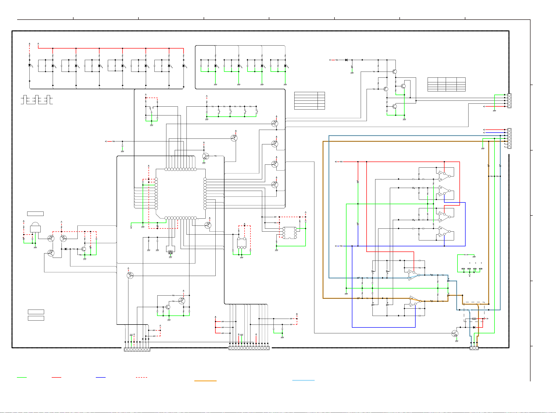
SCHEMATIC DIAGRAMS (1/3)
R ch SIGINAL LINE
SCHEMATIC DIAGRAMS (1/3)
MAIN UNIT
45
Page 46
5VD
87654321
5VL
STANDBY
R1501
D1501
STB
5V
1mS
7mS
0V
IC61 38 pin WAVE FORM at STAND BY mode
CUSHION_IR
R94EV1A
5VL
100
R1601
C1601
100/16
PHONO CDTUNER AUX/DVD REC1/CD-R REC2/MD/TAPE
820
C1501
SLR342VC
0.01
7mS
R1502
1mS1mS
10K
R1503
D1502
PHONO
330
C1502
SELG6E10C-S20
0.01
R1504
10K
R1505
D1503
TUNER
330
C1503
0.01
10K
R1506
R1507
D1504
SELG6E10C-S20
CD
Z1602
Q1601
Q1602
5VL
R1602
D1601
1SS133
100
KRA102S
Q1603
KTC3875S
R1603
47K
Q1604
R1604
18K
R1605
47K
0.1Z
C1604
C1603
100/16
U1601
VCC
3
2
0.1Z
C1602
D-GND
KRA102S
GND
Vout
1
KRA102S
D-GND
Z1601
OPEN
Z1603
OPEN
FRONT PWB
8U-110005-1
GND POWER + POWER -
5VD
330
C1504
SELG6E10C-S20
RC5_OUT
RC5_IN
KILL_IR
0.01
R1017
100
RC5
R1508
D1505
10K
D-GND
RC5_OUT
330
R1509
0
C1505
0.01
SELG6E10C-S2
AUX
0.1Z
C1010
STB
PHONO
CD
TUNER
AUX
REC1
REC2
MUTE
OPEN
B1005
NC
5VL
KRA102S
Q1001
RC5
5VL
D-GND
1
2
3
4
RC5
P_ON
+5VL
D_GND
To STANDBY PWB N8504
330
R1511
D1506
10K
R1510
REC1
5VL
R1411
47K
S1411
0.01
C1411
D-GND
5VL
0.1Z
C1002
D-GND
R1903
D-GND D-GND
0V:POWER ON
RXD
TXD
5
6
7
8
B1001
9P-WIRE
RXD9TXD
ICE4
P_DOWN
P_RELAY
STBY POWER
C1506
SELG6E10C-S20
47K
R1901
47K
R1902
47K
10K
R1512
0.01
47K
R1412
0.01
C1412
33
VAREF
34
AVDD
35
AVSS
36
LED_STD
37
LED_PHONO
38
LED_CD
39
LED_TUNER
40
LED_AUX/DVD
41
LED_REC1
42
LED_REC2
43
LED_MUTE
44
C1001
10/63
C1902
0.1Z
8.00M
KTC3875S
Q1002
0.1Z
R1001
C1003
5VL
R1513
D1507
REC2
32
SPK_B
VSS
2
1
X1001
123
D-GND
R1002
10K
D-GND
330
KILL_IR
31
M_MUTE
KILL_IR
XIN
XOUT
3
R1003
1M
33K
KRA102S
SELG6E10C-S20
30
29
28
DET
ENC-2
U1001
TMP86FH47UG
VDD
TEST
4
5
Q1003
MUTE
D1508
27
ENC-1
PROT-1
6
5VL
R1514
MUTE
7
R1004
330
SLI-343V8RCT32
TXD
RXD
26
25
24
TACT
M_B_DOWN
BOOT-1/RXD
RESET9P_OFF10SPK_OUT
PROT-2
8
0.1Z
47K
C1004
SOURCE DIRECT SPK A SPK B LOUDNESS
C1507
0.01
R1515
10K
S-DI
R1516
D1509
330
SELG6E10C-S20
C1508
0.01
R1517
10K
SPK_A
R1518
D1510
330
SELG6E10C-S20
C1509
0.01
R1519
10K
D-GND D-GND D-GND D-GND
5VL
SOURCE DIRECT LOUDNESS SPK A SPK B
RC5_IN
D-GND
23
RC-5_IN
BOOT-2/TXD
LOUD
SO_DI
SPK_A
I2C_DATA
I2C_CLK
CE
CLK
P_ON
DI
VOL_DWN
VOL_UP
RC-5_OUT
11
KRA102S
Q1010
5V:MUTE
R1401
C1401
D-GND
5VD
R1016
KRC102S
47K
Q1009
22
21
20
19
18
17
16
15
14
13
12
5VL
0V:PROTECT
0V:PROTECT
R1402
10K
2.2K
0.01
0V:MUTE
+15V:No Signal
0V :Signal Det
R1015
22K
A_MUTE
PROT_2
PROT_1
S1401
DET
CLK
DATA
R1403
3.9K
CE
S1402
KRA102S
Q1004
F_MUTE
SPK_B
SPK_A
R1404
3.9K
5VD
C1007
R1405
R1010
0.1Z
R1406
3.9K
22K
S1403
0V:LOUDNESS ON
0V:SOURCE DIRECT ON
0V:SPK_A ON
5VL
4.7K
5
4
OUT
VCC
NC
SUB
G
U1002
BD4742G
1
2
3
C1008
S1404
0V:SPK_B ON
0.1Z
D-GND
CECE
CLK
DATA
F_MUTE
A_MUTE
5VD
D-GND
3
4
5
6
CLK
+5VD
D-GND
F_MUTE7A_MUTE8PROT_1
To MAIN PWB N3002
PROT_1
9
P_RALAY
+12V
10
+12V
5VD
10K
10K
10K
R1005
R1006
R1007
1CE2
DATA
L ch SIGINAL LINE
SPK_B
R1520
D1511
SPK_A
PROT_2
11
12
SPK_A13SPK_B
PROT_2
330
SELG6E10C-S20
KRA102S
Q1005
KRA102S
Q1006
KRA102S
Q1007
KRA102S
Q1008
DET
SPK_B
14
DET
R1521
C1510
0.01
5VD
5VD
5VD
5VD
VOL_DOWN
VOL_UP
R1011
47K
R1012
10K
R1013
D-GND
C1005
0.1Z
B1002
14P-WIRE
LOUD
10K
SPK_B
LOUD
S-DI
SPK_A
47K
C1006
D-GND
330
R1522
D1512
SELG6E10C-S20
VOL_DOWN
VOL_UP
LOUD
S-DI
AT24C04AN
U1003
6
7
8
R1008
47K
R1009
47K
0.1Z
IC61 PIN26 A/D VOLTAGE
45
3
2
1
5VL
1.OFF(PULL UP)
2.SPK B
3.SPK A
4.LOUDNESS
5.SOURSE DIRECT
6.RESERVED 0V
5.0V
3.9V
2.9V
1.9V
0.9V
5VL
0.1Z
R1014
C1009
47K
D1801
R1801
5VD
10
1N4003
C1801
220/6.3
D-GND
R2021
+15V
10
C2019
C2020
R2022
-15V
10
C2003
10/50
A-GND
C2004
10/50
R ch SIGINAL LINE
R1802
R1803
47/50
47/50
TREBLE BASS
R2005
2.7K
100K
R2003
100K
R2004
R2006
2.7K
TREBLE
2.2K
2.2K
6
4
V2002
C2005
C2006
1
3
V2002
10K
220P
220P
10K
R1804
R1805
5
2
A
47K
Q1801
KTA1271Y
R1807
R1809
R1806
Q1802
KTA1271Y
R1808
2.2K
47K
2.2K
47K
Q1804
KTC3203Y
Q1803
KTC3203Y
47K
VOL_DOWN 4.4V 4.4V 0V
VOL_UP 4.4V 0V 4.4V
MOT- 0V 0V 4.4V
MOT+ 0V 4.4V 0V
D-GND
1.2K
R2015
C2013
C2017
0.01
220P
C2011
C2015
R2019
0.068
V2003
V2003
BASS
2.2/50
C2012
2.2/50
C2014
0.01
C2007
10K
6
5
4
1
2
3
10K
6
8
5
3
4
2
C2008
1.2K
R2013
1.2K
R2014
C2016
0.068
C2018
220P
1.2K
R2016
220P
R2007
2.7K
7
U2001
AZ4580MTR
U2001
AZ4580MTR
1
R2008
2.7K
220P
56K
R2017
R2018
56K
C2009
22/50
C2010
22/50
R2020
6
5
47K
3
2
6
5
47K
3
2
R2011
R2009
R2010
R2012
STOP
TREBLE
BASS
BASS
TREBLE
220
100K
100K
220
VOL
U/D
8
7
(2/2)
U2002
AZ4580MTR
(1/2)
1
4
8
7
(2/2)
U2003
AZ4580MTR
(1/2)
1
4
BALANCE
4
6
V2001
1
3
V2001
KRC102S
Q2001
5
2
VOL
U/D
TREBLE:15kHz ± 10dB
BASS:50 Hz ± 10dB
J2001
SHORT
V2003
S1411
FG9FG
4
8
5
OPEN.
B1004
20K
TO CHASSIS
20K
13
D-GND
7 7
V2002
FG9FG
8
BC3/12V
S2001
911
16
D2001
1SS133
1
+15V
-15V
4
+12V
A-GND
V2001
FG9FG
8
86
5P-WIRE
B1006
5
D-GND
4
MOT+
3
MOT-
2
LOUD
1
+12V
D-GND
B
N1002
7P-BtoB-CON
1
+15V
2
-15V
3
TO_L
4
A_GND
5
TO_R
6
C2002
R2002
56K
10/50
R2001
56K
C2001
7
10/50
From VOLUME PWB N5002 From VOLUME PWB N5001
C
D
7
E
+12V
D-GND
1
2
3
B1003
L
R
3P-SHIELD-WIRE
A_GND
To MAIN PWB N6001
F
SCHEMATIC DIAGRAMS (2/3)
SCHEMATIC DIAGRAMS (2/3)
FRONT UNIT
46
Page 47
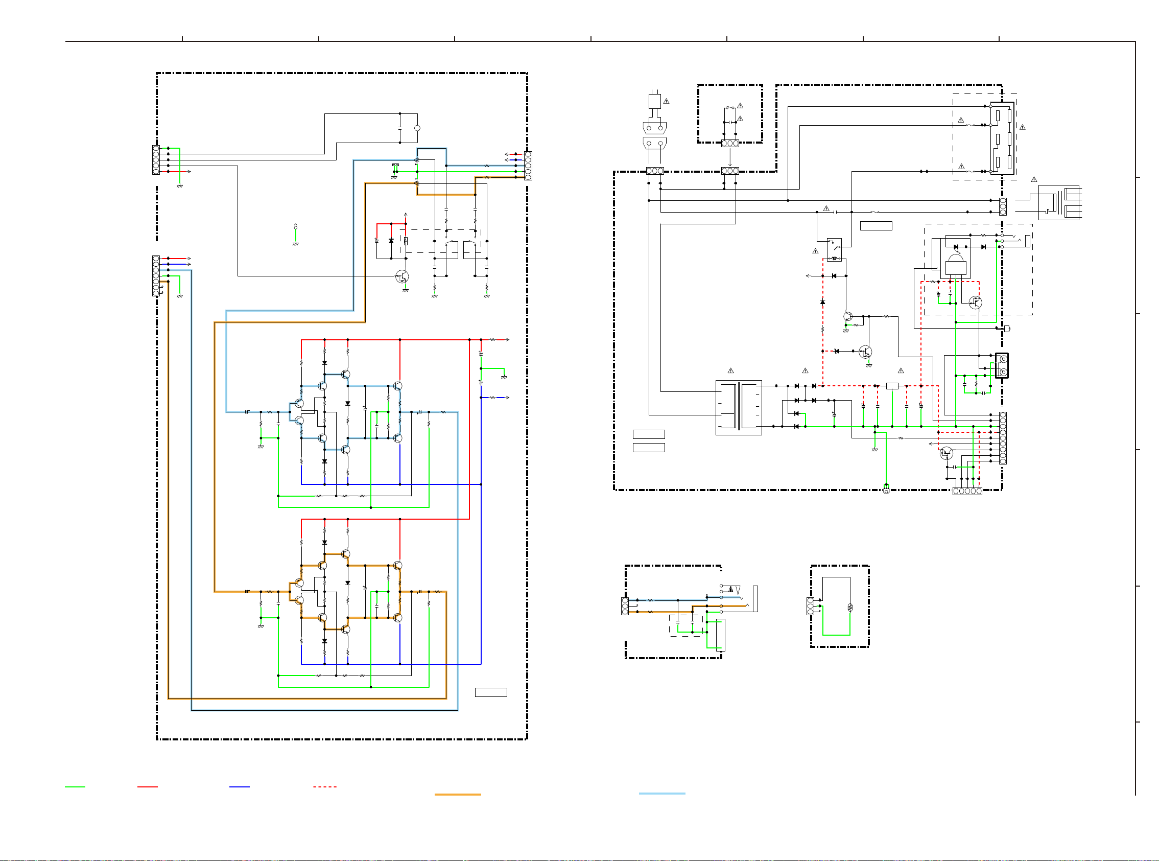
5P-BASE
87654321
N5001
5
D_GND
4
MOT+
3
MOT-
2
LOUD
1
+12V
From FRONT PWB B1006
N5002
7P-PINHEADER
1
+15V
2
-15V
3
TO_L
4
A_GND
5
TO_R
6
To FRONT PWB N1002
7
D-GND.
A-GND.
+12V.
+15V.
-15V.
C5001
10/35
C5002
10/35
R5005
R5003
A-GND.
R5006
R5004
A-GND.
100
56K
100
56K
C5003
C5004
TO CHASSIS
B5002
1PIN-WIRE
A-GND.
100P
100P
R5011
R5007
R5009
R5013
R5012
R5008
R5010
R5014
12K
22
Q5001
KTA1268GR
Q5003
22
KTC3200GR
12K
R5041
100
12K
22
Q5002
KTA1268GR
Q5004
22
KTC3200GR
12K
R5042
100
R5019
R5015
R5017
R5021
R5020
R5016
R5018
R5022
470
D5001
1SS133
Q5005
KTC3200GR
22
22
Q5007
KTA1268GR
D5003
1SS133
470
R5043
220
470
D5002
1SS133
Q5006
KTC3200GR
22
22
Q5008
KTA1268GR
D5004
1SS133
470
R5044
220
R5025
D5005
R5023
R5027
R5026
D5006
R5024
R5028
220
Q5009
KTA1268GR
1SS133
C5005
180
Q5011
KTC3200GR
220
R5045
270
220
Q5010
KTA1268GR
1SS133
C5006
180
Q5012
KTC3200GR
220
R5046
270
C2505
10/50
C5007
10/50
C5008
A-GND.
OPEN
D2501
KRC102S
Q2501
R5029
100P
R5031
R5030
100P
R5032
11
1M
1M
1M
1M
+
10
0.01
M
9
C5013
-
V5001
7
8
6
5
12
V5001
1
2
4
3
+12V.
BC3/12V
S2501
1
16
1SS133
D-GND.
A-GND. A-GND.
Q5013
KTC3200GR
33
C5009
R5033
47/25
33
R5035
R5037
Q5015
KTA1268GR
Q5014
KTC3200GR
33
C5010
R5040
R5034
47/25
33
R5036
R5038
Q5016
KTA1268GR
C2503
R2503
R5039
100K
220
100K
0.1
5.6K
220
POWER SW PWB
8U-110005-4
(U version only)
S8901
W0001
Z8501
Z8502
J0001
W0002
1
2
5P-SHIELD-WIRE
B5001
+15V.
-15V.
1
2
3
4
5
To MAIN PWB N3001
2P-BASE
N8501
OPEN
OPEN
+15V.
-15V.
R5001
330
R5002
330
1000P
1000P
C2502
C2501
R2501
911
3.3K
3.3K
R2502
86
4
13
0.1
C2504
5.6K
R2504
R5047
SHORT
C5011
220/25
A-GND.
C5012
220/25
R5048
SHORT
STANDBY PWB
8U-110005-3
HEADPHONE PWB
8U-110005-5
3P-WIRE
B9901
R9901
1
Z5001
STYLE-PIN
HP_L
NC
HP_R
To MAIN PWB N7501
47
2
R9902
3
47
0.01
C9902
C9901
C9901/C9902:N/K ONLY
12
C8901
470P/250V
3
1
4
3
2
1
HP-JACK(SILVER_PLATE)
K9901
0.01
Z9901
SHIELD-PLATE(HP)
1
B8901
2P-WIRE
2P-BASE
N8502
2
T8501
TO CHASSIS
C8502
0.0047/250V
DLS6D1-0(M)
S8501
4
3
1
2
D8507
R8501
D8508
1SS133
SHORTSHORT
Q8501
KTC3198GR
D-GND..
P_RELAY
D8509
UDZS11B
1N4003
D8501
6
5
7
9
8
D8502
D8503
D8504
D8505
D8506
1/50
C8503
POSISTER PWB
8U-110005-6
3P-WIRE
B6501
1
HEAT
2
GND
3
NC
To MAIN PWB N9001
H8511
H8512
F8510
T3.15A/L250V
N/K version:T1.6AL 250V
U version:T3.15AL 250V
R8502
R8505
47K
Q8502
KRC102S
D-GND..
IN
C8504
C8510
2200/25
D-GND..
CHASSIS
B8501
T6501
4.7K
BA50BC0FP
U8501
OUT
0.1Z
R8503
82K
C8505
P_RELAY
0.1Z
(U version only)
SIR-34ST3F
9999999999
Z8701
SHIELD-CASE
R8702
100
C8701
100/16
C8506
220/6.3
Q8503
KRA102S
D8701
VCC
3
C8702
C8509
0.1Z
F8610
T5.0A/250V
F8620
T5.0A/250V
GND
Vout
2
1
0.1Z
0.1Z
C8508
3
4
5
TXD
RXD
ICE4
UPDATE
R8701
100
D8702
1SS133
U8701
R94EV1A
Q8701
47
C8507
R8504
0.1Z
1
2
N8505
5P-FMNs
+5VL
D_GND
1
1
2
2
3
3
KRA102S
1
4
2
3
K8601
AC-OUTLET-110V(3P)
AC Outlets
N8503
2P-BASE-BOX
1
2
K8701
2
2
3
3
1
1
B8502
CMD1A569
K8501
IN
RC5
OUT
9P-BASE
N8504
1
RC5
2
P_ON
3
D_GND
4
+5VL
5
P_DOWN
6
P_RELAY
7
ICE4
8
RXD
9
TXD
MAIN TRANSFORMER
T0001
Flasher Input
MINI-JACK(PJ-308-02)
From FRONT PWB B1001
A
B
C
D
E
GND POWER + POWER -
STBY POWER
VOLUME PWB
8U-110005-2
L ch SIGINAL LINE
47
R ch SIGINAL LINE
SCHEMATIC DIAGRAMS (3/3)
VOLUME UNIT
STANDBY UNIT
POWER SW UNIT
HEADPHONE UNIT
SCHEMATIC DIAGRAMS (3/3)
POSISTER UNIT
F
Page 48

WIRING DIAGRAM
Main Trans
HEADPHONE
PWB
8U-110005-5
N8001
N8101
N6003N6004
POSISTER
PWB
8U-110005-6
B6501
MAIN PWB
8U-110004-1
N9001
AC INLET
N8501
POWER SW PWB
8U-110005-4
B8901
N8503 N8502
B9901
N7501
Idling test point Idling test point
N3002
B1002
N6001
B1003
B1006
N3001
B5001
N5001
STANDBY PWB
8U-110005-3
N8505
Soft Update
N8504
B1001
FRONT PWB
8U-110005-1
48
N1002
N5002
B5002
VOLUME PWB
8U-110004-2
Page 49

EXPLODED VIEW
39
x2
38
x2
S2
S1
36
44
S2
34
S1
33
S1
S1
x2
S1
x2
S1
32
x5
S1
31
S1
S3
S8
x2
x3
37
24
S2
x2
S1
14
15
S1
6
8
S1
12
13
18
x2
S1
17
16
x12
S6
19
S1
z
27
x4
S11
x4
S10
35
29
S9
40
S5
x2
S5
41
x6
S1
S7
S1
42
26
x7
S4
S7
S9
25
S2
S9
28
37
S3
S1
9
4
1
2
3
5
x5
S1
22
S6
S1
11
S1
x6
10
x2
S7
S1
8
7
20
22
21
x4
S1
23
S1
23
30
x4
S1
30
WARNING:
Parts marked with this symbol have critical
characteristics.
Use ONLY replacement parts recommended by
the manufacturer.
49
Page 50

Personal notes: Personal notes:
50
Page 51

PARTS LIST OF EXPLODED VIEW
Parts indicated by "nsp" on this table cannot be supplied.
z
P.W.B. ASS'Y indicated by "nsp" on this table cannot be supplied. When repairing the P.W.B. ASS'Y, check the board parts list and order replacement parts.
z
Parts indicated by the "★" mark are not illustrated in the exploded view.
z
The parts listed below are only for maintenance. Therefore they might differ from the parts used in the unit in appearances or dimensions.
z
Note: The symbols in the column "Remarks" indicate the following destinations.
U : North America model N : Europe model K : China model
B : Black model SG : Silver gold model
Ref. No. Part No. Part Name Remarks Q'ty New
25 nsp MAIN PWB ASSY N,K 1 *
25 nsp MAIN PWB ASSY U 1 *
A nsp FRONT PWB ASSY N,K 1 *
A nsp FRONT PWB ASSY U 1 *
14 - POWER SW PWB UNIT
15 - HEADPHONE PWB UNIT
18 - FRONT PWB UNIT
19 - VOLUME PWB UNIT
29 - STANDBY PWB UNIT
1 421410006004M MARANTZ BADGE (AL) FOR M1 MODEL 1
2 41651000300AM WINDOW FUNCTION PM6004 1
3 412510059003M TONE KNOB BL PM7004 A334 N1B,U1B,K1B 3
3 412510059034M TONE KNOB SG PM7004 A334 N1SG 3
4 40241001600AM FRONT AL PANEL BL PM6004 N1B,U1B,K1B 1 *
4 40241001601AM FRONT AL PANEL SG PM6004 N1SG 1 *
5 nsp FRONT CENTER MOLD BL PM6004 N1B,U1B,K1B 1
5 nsp FRONT CENTER MOLD SG PM6004 N1SG 1
6 402510154000M CGW3A467RNXB37 ESC. L BL PM5004 A333 N1B,U1B,K1B 1
6 402510154031M
7 40251001700AM ESCUTCHEON R BL PM6004 N1B,U1B,K1B 1
7 40251001701AM ESCUTCHEON R SG PM6004 N1SG 1
8 42451000200AM RING VOLUME BL PM6004 N1B,U1B,K1B 2
8 42451000201AM RING VOLUME SG PM6004 N1SG 2
9 41201000200AM KNOB AL CAP BL PM6004 N1B,U1B,K1B 1
9 41201000201AM KNOB AL CAP SG PM6004 N1SG 1
10 41201000300AM KNOB AL CAP POINTER BL PM6004 N1B,U1B,K1B 1
10 41201000301AM KNOB AL CAP POINTER SG PM6004 N1SG 1
11 481510004009M LENS IR BL PM7003 24AJ N1B,U1B,K1B 1
11 481510004047M LENS IR WH PM7003 24AJ N1SG 1
12 481510003006M LENS 1
13 411510027003M BUTTON PUSH BL PM7003 24AJ N1B,U1B,K1B 1
13 411510027034M BUTTON PUSH SG PM7003 24AJ N1SG 1
16 nsp LENS FUNCTION A349 1
17 41151000200AM BUTTON BL PM6004 N1B,U1B,K1B 1
17 41151000201AM BUTTON SG PM6004 N1SG 1
20 nsp FRONT FRAME 1
21 nsp MAIN CHASSIS PM6004 A349 1
22 nsp BUFFER 2
23 00M243W057210 FOOT SL 4
24 nsp HOLDER h119 2
26 45351000200AM CAP PM6004 A349 N,K 8
z
27 10101000600AM POWER TRANS (U) A349 U 1 *
CGW3A467ROWD10 ESC. L SG PM5004 A333
N1SG 1
51
Page 52

Ref. No. Part No. Part Name Remarks Q'ty New
z
z
27 10101000500AM POWER TRANS (N) A349 N,K 1
28 nsp HOLDER h5 2
30 00M32CW107010 CUSHION FOOT CHG1A360 4
31 nsp REAR PANEL PM6004 (U) U 1 *
31 nsp REAR PANEL PM6004 (N) N 1 *
31 nsp REAR PANEL PM6004 (K) K 1 *
32 48801000200AM Terminal PHONO 1
33 00D2033996008 AC INLET (2P) 1
34 40331000300AM TOP COVER BL PM6004 N1B,U1B,K1B 1
34 40331000301AM TOP COVER SG PM6004 N1SG 1
35 nsp RUBBER PM6004 A349 2
36 nsp LABEL (HOT SURFACE CAUTION) 1
37 00M14AJ107010 TOP COVER SHEET 3
38 44551000200AM SHEET TOP BL PM6004 A349 N1B,U1B,K1B 1
38 44551000201AM SHEET TOP SG PM6004 A349 N1SG 1
39 45451000500AM STOPPER TOP BL PM6004 A349 N1B,U1B,K1B 2
39 45451000501AM STOPPER TOP SG PM6004 A349 N1SG 2
40 nsp MAIN HEATSINK PM6004 A349 1
41 nsp HEATSINK BRACKET F PM6004 1
42 nsp HEATSINK BRACKET R PM6004 1
44 419510012005M MASK TOP LID REAR 1
45 00D4458004007 WIRE CLAMPER 9
★
SCREWS
WIRES
S1 nsp SCREW 51
S2 nsp SCREW BK 6
S2 nsp SCREW (SELF TAPPING) SG 6
S3 nsp B.T.SCREW EX600240 2
S4 nsp SCREW 7
S5
S6 nsp SCREW 13
S7 nsp SCREW 4
S8 nsp SCREW 2
S9 nsp SCREW 4
S10 nsp SCREW 4
S11 nsp 4X6 CBTS (S)-B 4
W0002 0120109160060
★
nsp SCREW 3
VAR-NO CN7.92MMPICH1PIN:BR.2PIN:BL10CM
1
52
Page 53

PACKING VIEW
z
PARTS LIST OF PACKING & ACCESSORIES
Parts indicated by "nsp" on this table cannot be supplied.
z
Parts indicated by the "★" mark are not illustrated in the exploded view.
z
The parts listed below are only for maintenance. Therefore they might differ from the parts used in the unit in appearances or dimensions.
z
Note: The symbols in the column "Remarks" indicate the following destinations.
U : North America model N : Europe model K : China model
B : Black model SG : Silver gold model
Ref. No. Part No. Part Name Remarks Q'ty New
201 54111000202AM USER MANUAL PM6004 (U) A349 U 1 *
201 54111000200AM USER MANUAL PM6004 (N) A349 N 1 *
201 54111000205AM USER MANUAL PM6004 (K) A349 K 1 *
z
z
z
202 00MZC01803100 # AC CORD UL/CSA 10A 125V U 1
202 00MZC01803080 # 2P AC CORD 10A 250V CLASS2 N 1
202 00D2062249001 AC CORD (E1C) K 1
203 nsp BATTERY(R03X2) 1
204 307010030006M RC003PM 1
205 nsp WARRANTY USA U 1
53
Page 54

Ref. No. Part No. Part Name Remarks Q'ty New
206 nsp WARRANTY CANADA U 1
207 53361000800AS CUSHION 2 *
208 53121000800AM PACKING CASE PM6004 A349 1 *
209 nsp CONT.LABEL BASE(D&M) 1
210 nsp POLYETHY BAG 1
★
211 nsp CABINET COVER 1
★
212 nsp CLEAR LABEL(44X12 T0.05) U 1
★
213 nsp LABEL FOR PKG SG N1SG 2
★
54
Page 55

SEMICONDUCTORS
TMP86FH47
TMP86FH47
Block Diagram
Only major semiconductors are shown. General semiconductors etc. are omitted from list.
The semiconductors which have a detailed drawing in a schematic diagram are omitted from list.
1. IC's
ETMP86FH47UG (U1001)
Block Diagram
RESET
TEST
XIN
XOUT
Program memory
(Flash memory)
Flash memory I/F
Standby control
circuit
System control
circuit
Timing generator
High
frequency
Clock
generator
Low
frequency
P2
TLCS-870/C
CPU
Time base
timer
Watchdog
timer
P1 P4 P0 P 3
P47 to P40 P37 to P30
I/O ports
16-bit
timer/counter
TC1
Address/data bus
P07 to P00 P22 to P20 P17 to P10
Address/data bus
Data memory
(RAM)
Interrupt controller
8-bit
timer/counter
TC3
TC4
Boot program
(ROM
SIO
)
10
-bit AD
converter
AVSS
AVDD
VAREF
UART
55
Page 56

Terminal Functions
Pin Port Name I/O Use Name
1 VSS - - - - - - 0 V
2 XIN - - - - - - 8M Clock in
3 XOUT - - - - - - 8M Clock out
4 TEST I I H - L 47k L->H : PROM Mode(Program rewriting)
5 VDD - - VDD - - - - u-com power supply 5V
6 P21 (XTIN) I/O I PROT-1 L - H 47k
7 P22 (XTOUT) I/O I PROT-2 L - H 47k PROTECT_2:Vol.tage Abnormal Detect
8 RESET I/O I L - H 4.7k u-com Reset connector
9 P20 (STOP/INT5) I/O I P_OFF L - H 47K Detect Power Down(primary power supply ON/
10 P00 (INT0) I/O O SPK_OUT L H H - Speaker Relay On (Audio Out)
11 P01
(TC4/PD04/PPG4/PWM4)
12 P02 (RXD) I/O O VOL_UP L H H 47K Volume up
13 P03 (TXD) I/O O VOL_DWN L H H 47K Volume down
14 P04 (SO) I/O O DI - L L 10K Data (LC78212)
15 P05 (SI) I/O O P_ON L H H - Primary Relay ON
16 P06 (SCK) I/O O CLK - - L 10K Clock (LC78212)
17 P07 (INT4) I/O O CE H L L 10K CE (LC78212)
18 P17 I/O O I2C_CLK - H H 47k I2C (EEPROM) (Pull up)
19 P16 I/O I/O I2C_DATA - H H 10K I2C (EEPROM) (Pull up)
20 P15 (INT3) I/O O SPK_A L H H - Speaker A Relay On
21 P14 (PPG) I/O O SD_DI L H H - Relay operation port on power amp direct source
22 P13 (DVO) I/O O PA_DI L H H - Relay operation port on power amp direct
23 P12 (INT2/TC1) I/O I RC-5_IN L - H 47k RC-5 Input
24 P11 (INT1)(BOOT2) I/O I BOOT-2/
25 P10(PWM3/TC3/PD03)
(BOOT1)
26 P30 (AIN0) I/O I
27 P31 (AIN1) I/O I M_B_DOWN L - H 47k Checking port for amp power supply off conrm
28 P32 (AIN2) I/O I ENC_1 L - H 47k Input Sel. Rotary Enc.
29 P33 (AIN3) I/O I ENC_2 L - H 47k Input Sel. Rotary Enc.
30 P34 (AIN4/STOP2) I/O I DET L - L 47k Power down : L (for Signal detection circuit)
31 P35 (AIN5/STOP3) I/O O KILL IR H L L - RC-5 Kill
32 P36 (AIN6/STOP4) I/O O M_MUTE L H L - Manual Mute (Mute on :L)
33 P37 (AIN7/STOP5) I/O O SPK_B L H H - Speaker B Relay On
34 VAREF - - VAREF - - - - A/D Reference
35 AVDD - - AVDD - - - - 5 V
36 AVSS - - AVSS - - - - 0 V
37 P40 I/O O LED_STD L H L - STANDBY LED/Protecting warning ushes
38 P41 I/O O
39 P42 I/O O LED_CD L H H - CD LED
40 P43 I/O O
41 P44 I/O O LED_AUX/
42 P45 I/O O LED_REC1 L H H - REC1 LED
43 P46 I/O O LED_REC2 L H H - REC2 LED
44 P47 I/O O LED_MUTE L H H - MUTE LED/Protecting1 warning ushes
I/O O RC-5_OUT L H H - RC-5 Output
TXD
I/O I BOOT-1/
RXD
TACT - - - 10K Source Direct / Power Amp Direct SW /SPK A /
(AD)
LED_PHONO
LED_TUNER
DVD
Port Setting
ACT INIT STBY EXT.R
PROTECT_1: DC Offset / Over Current / Over Current
OFF detection).
Oveserve at power supply cutting, Interrupt input
direct mode
- - - 47k Pull Up
- - - 47k Pull Up
SPK B
L H H - PHONO LED
L H H - TUNER LED
L H H - AUX/DVD LED
Note
56
Page 57

LC78212 (U3501)
LC78211, 78212, 78213
57
Page 58

PARTS LIST OF P.C.B. UNIT
Parts indicated by "nsp" on this table cannot be supplied.
z
The parts listed below are only for maintenance. Therefore they might differ from the parts used in the unit in appearances or dimensions.
z
Note: The symbols in the column "Remarks" indicate the following destinations.
U : North America model N : Europe model K : China model
B : Black model SG : Silver gold model
8U-110004A MAIN PWB UNIT ASS'Y (N,K model) 8U-110004B MAIN PWB UNIT ASS'Y (U model)
Ref. No. Part No. Part Name Remarks Q'ty New
SEMICONDUCTORS GROUP
D3501 20105001130AS 1SS133(HOMI)
D3901-3903 20105001130AS 1SS133(HOMI)
D6001-6012 20105001130AS 1SS133(HOMI)
D7501-7503 20105001130AS 1SS133(HOMI)
z
D8001 20305000320AS KBU804 BRIDGE DIODE
z
D8101-8104 00MHD20055101 !SHOTTKY 11EQS10 1A 100V
D8105,8106 20305002730AS 1N4003(HOMI)
z
D8201,8202 20305002730AS 1N4003(HOMI)
D9001,9002 20105001130AS 1SS133(HOMI)
U3501 00MHC10309030 IC LC78212:CMOS LOGIC SANYO
U3801 00D2631289900 AZ4580MTR-E1
U3901 00D2631289900 AZ4580MTR-E1
U4001 00D2630896909 NJM2068MD-TE1 +C
U8101 00D2631100034 KIA7815API-U/P
U8102 00D2631099035 KIA7915PI-U/P
U8201 00D2631100021 KIA7812API-U/P
U8202 00D2631100005 KIA7805API-U/P
Q6001,6002 00D2730459903 KTC2874-B-AT/P
Q6003,6004 00MHT600121A1 KTA1268 PNP TRANSISTOR RANK=GR
Q6005-6008 00MHT800931A1 KTC3200 NPN TRANSISTOR RANK=GR
Q6009,6010 00MHT600121A1 KTA1268 PNP TRANSISTOR RANK=GR
Q6011,6012 00MHT800931A1 KTC3200 NPN TRANSISTOR RANK=GR
Q6013-6016 00MHT600121A1 KTA1268 PNP TRANSISTOR RANK=GR
Q6017,6018 00MHT800931A1 KTC3200 NPN TRANSISTOR RANK=GR
Q6019,6020 00D2710168900 2SA1145 (O)/(Y)TPE6
Q6021,6022 00D2730281919 2SC2705 (Y)TPE6
Q6023,6024 21305001240AS KTC3198-GR-AT/P
Q6025-6028 00D2710300904 KTA1266-GR-AT/P
Q6029,6030 21305001240AS KTC3198-GR-AT/P
Q6031,6032 00MHT334191Y0
Q6033,6034 00D2730281919 2SC2705 (Y)TPE6
Q6035,6036 00D2710168900 2SA1145 (O)/(Y)TPE6
z
Q6110 00MHK136019C0 2SA/360/2SC3423 PAIR O OR Y
z
Q6120 00MHK136019C0 2SA/360/2SC3423 PAIR O OR Y
z
Q6130 21905000200AS 2SA1694/2SC4467 PAIR
z
Q6140 21905000200AS 2SA1694/2SC4467 PAIR
Q7501 00D2710300904 KTA1266-GR-AT/P
Q7502 00D2690206908 KRC102M-AT/P (10K-10K)
Q7503 21305001240AS KTC3198-GR-AT/P
Q7504 21305001240AS KTC3198-GR-AT/P
Q7505 00D2690206908 KRC102M-AT/P (10K-10K)
TRANSISTOR C3419 Y 40V 0.8A PC=1.2W (5W)
58
Page 59

Ref. No. Part No. Part Name Remarks Q'ty New
Q9001 21305001240AS KTC3198-GR-AT/P
Q9002 21305001240AS KTC3198-GR-AT/P
Q9003 00D2710300904 KTA1266-GR-AT/P
Q9004 00D2730464901 KTC3875S-GR-RTK/P
Q9005 00D2730464901 KTC3875S-GR-RTK/P
Q9006 00D2730464901 KTC3875S-GR-RTK/P
Q9007 00D2710312905 KTA1504S-GR-RTK/P
Q9008 00D2690192902 KRC102S-RTK/P (10K-10K)
Q9101 00D2730464901 KTC3875S-GR-RTK/P
Q9102 00D2730464901 KTC3875S-GR-RTK/P
Q9103 00D2710312905 KTA1504S-GR-RTK/P
RESISTORS GROUP
R3805 00MGG0510016X 10 OHM +- 5% 1/6W FLAMERETERDANT
R3806 00MGG0510016X 10 OHM +- 5% 1/6W FLAMERETERDANT
R4021 00MGG0510016X 10 OHM +- 5% 1/6W FLAMERETERDANT
R4022 00MGG0510016X 10 OHM +- 5% 1/6W FLAMERETERDANT
R6031 00MGG0547116X 470 OHM +- 5% 1/6W FLAMERETERDANT
R6032 00MGG0547116X 470 OHM +- 5% 1/6W FLAMERETERDANT
R6033 00MGG0547116X 470 OHM +- 5% 1/6W FLAMERETERDANT
R6034 00MGG0547116X 470 OHM +- 5% 1/6W FLAMERETERDANT
R6035 00MGG0515116X 150 OHM +- 5% 1/6W FLAMERETERDANT
R6036 00MGG0515116X 150 OHM +- 5% 1/6W FLAMERETERDANT
R6037 00MGG0515116X 150 OHM +- 5% 1/6W FLAMERETERDANT
R6038 00MGG0515116X 150 OHM +- 5% 1/6W FLAMERETERDANT
z
R6073 00MGG0522016X 22 OHM +- 5% 1/6W FLAMERETERDANT
z
R6074 00MGG0522016X 22 OHM +- 5% 1/6W FLAMERETERDANT
z
R6075 00MGG0522016X 22 OHM +- 5% 1/6W FLAMERETERDANT
z
R6076 00MGG0522016X 22 OHM +- 5% 1/6W FLAMERETERDANT
R6077 00MGG0510116X 100 OHM +- 5% 1/6W FLAMERETERDANT
R6078 00MGG0510116X 100 OHM +- 5% 1/6W FLAMERETERDANT
R6079 00MGG0510116X 100 OHM +- 5% 1/6W FLAMERETERDANT
R6080 00MGG0510116X 100 OHM +- 5% 1/6W FLAMERETERDANT
R6081 00MGG0510216X 1K OHM +- 5% 1/6W FLAMERETERDANT
R6082 00MGG0510216X 1K OHM +- 5% 1/6W FLAMERETERDANT
R6083 00MGG0547016X 47 OHM +- 5% 1/6W FLAMERETERDANT
R6084 00MGG0547016X 47 OHM +- 5% 1/6W FLAMERETERDANT
R6085 00MGG0547016X 47 OHM +- 5% 1/6W FLAMERETERDANT
R6086 00MGG0547016X 47 OHM +- 5% 1/6W FLAMERETERDANT
R6087 00MGG0522116X 220 OHM +- 5% 1/6W FLAMERETERDANT
R6088 00MGG0522116X 220 OHM +- 5% 1/6W FLAMERETERDANT
R6089 00MGG0510016X 10 OHM +- 5% 1/6W FLAMERETERDANT
R6090 00MGG0510016X 10 OHM +- 5% 1/6W FLAMERETERDANT
R6091 00MGG0510016X 10 OHM +- 5% 1/6W FLAMERETERDANT
R6092 00MGG0510016X 10 OHM +- 5% 1/6W FLAMERETERDANT
z
R6093 00D2462099013 RK92=3AR22JS
z
R6094 00D2462099013 RK92=3AR22JS
z
R6095 00D2462099013 RK92=3AR22JS
z
R6096 00D2462099013 RK92=3AR22JS
R6105 00MNK05100020 10 OHM +- 5% 2W
R6106 00MNK05100020 10 OHM +- 5% 2W
R7507 00MNK05331020 330 OHM +- 5% 2W
59
Page 60

Ref. No. Part No. Part Name Remarks Q'ty New
R7508 00MNK05331020 330 OHM +- 5% 2W
z
R8001 00MBF68400016 ! 0.68UF/4.7OHM
z
R8101 00MGG05010120 ERD50FJ1R0P or SPRX1CM12.5A J 1R0 FLAMERETERDANT
z
R8102 00MGG05010120 ERD50FJ1R0P or SPRX1CM12.5A J 1R0 FLAMERETERDANT
R9001 00MGG0510216X 1K OHM +- 5% 1/6W FLAMERETERDANT
R9002 00MGG0510216X 1K OHM +- 5% 1/6W FLAMERETERDANT
R9003 00MGG0515216X 1.5K OHM +- 5% 1/6W FLAMERETERDANT
R9004 00MGG0515216X 1.5K OHM +- 5% 1/6W FLAMERETERDANT
V6001 00MRA02210781 220OHM NVZ6TLTA B221
V6002 00MRA02210781 220OHM NVZ6TLTA B221
V6003 00MRA04720781 4.7KOHM NVZ6TLTA B472
V6004 00MRA04720781 4.7KOHM NVZ6TLTA B472
CAPACITORS GROUP
C3009 133050086503S CQ93M2A221JT(PEF) N,K
C3010 133050086503S CQ93M2A221JT(PEF) N,K
C3011 133050086503S CQ93M2A221JT(PEF) N,K
C3012 133050086503S CQ93M2A221JT(PEF) N,K
C3013 133050086503S CQ93M2A221JT(PEF) N,K
C3014 133050086503S CQ93M2A221JT(PEF) N,K
C3015 133050086503S CQ93M2A221JT(PEF) N,K
C3016 133050086503S CQ93M2A221JT(PEF) N,K
C3017 133050086503S CQ93M2A221JT(PEF) N,K
C3018 133050086503S CQ93M2A221JT(PEF) N,K
C3019 133050086503S CQ93M2A221JT(PEF) N,K
C3020 133050086503S CQ93M2A221JT(PEF) N,K
C3021 133050086503S CQ93M2A221JT(PEF) N,K
C3022 133050086503S CQ93M2A221JT(PEF) N,K
C3501 00MOA10605021 10 UF M 50V RA-2
C3502 00MOA10605021 10 UF M 50V RA-2
C3506 13405014040AS CE04W1H4R7MT(KR3)
C3801 00MOA10605021 10 UF M 50V RA-2
C3802 00MOA10605021 10 UF M 50V RA-2
C3803 00MOA10702521 100 UF M 25V RA-2
C3804 00MOA10702521 100 UF M 25V RA-2
C3901 133050086503S CQ93M2A221JT(PEF)
C3902 00MOA10605021 10 UF M 50V RA-2
C3904 13405014840AS CE04W1J100MT(KR3)
C4001 133050086503S CQ93M2A221JT(PEF) N,K
C4002 133050086503S CQ93M2A221JT(PEF) N,K
C4003 00MOA10605021 10 UF M 50V RA-2
C4004 00MOA10605021 10 UF M 50V RA-2
C4005 133050086503S CQ93M2A221JT(PEF)
C4006 133050086503S CQ93M2A221JT(PEF)
C4007 00MOA22702521 220 UF M 25V RA-2
C4008 00MOA22702521 220 UF M 25V RA-2
C4009 133050088516S CQ93M2A393JT(PEF)
C4010 133050088516S CQ93M2A393JT(PEF)
C4011 133050086527S CQ93M2A102JT(PEF)
C4012 133050086527S CQ93M2A102JT(PEF)
C4013 133050087544S CQ93M2A103JT(PEF)
60
Page 61

Ref. No. Part No. Part Name Remarks Q'ty New
C4014 133050087544S CQ93M2A103JT(PEF)
C4015 00MOA10605021 10 UF M 50V RA-2
C4016 00MOA10605021 10 UF M 50V RA-2
C4019 00MOA10702521 100 UF M 25V RA-2
C4020 00MOA10702521 100 UF M 25V RA-2
C6001 00MOA22605021 22 UF M 50V RA-2
C6002 00MOA22605021 22 UF M 50V RA-2
C6003 00MOF55101591 100PF 200V +- 10% FAS
C6004 00MOF55101591 100PF 200V +- 10% FAS
C6011 00MOA47706326 470 UF M 63V RA-2
C6012 00MOA47706326 470 UF M 63V RA-2
C6013 00MOA47706326 470 UF M 63V RA-2
C6014 00MOA47706326 470 UF M 63V RA-2
C6015 00MOF55331581 330PF 100V +- 5% FNS
C6016 00MOF55331581 330PF 100V +- 5% FNS
C6017 00MOA47602521 47 UF M 25V RA-2
C6018 00MOA47602521 47 UF M 25V RA-2
C6019 00MOA22702521 220 UF M 25V RA-2
C6020 00MOA22702521 220 UF M 25V RA-2
C6023 133050088516S CQ93M2A393JT(PEF)
C6024 133050088516S CQ93M2A393JT(PEF)
C7501 133050087544S CQ93M2A103JT(PEF) N,K
C7502 133050087544S CQ93M2A103JT(PEF) N,K
C7503 133050087544S CQ93M2A103JT(PEF) N,K
C7504 133050087544S CQ93M2A103JT(PEF) N,K
z
C8001 13405000220AS 10000UF/63V(LAO)
z
C8002 13405000220AS 10000UF/63V(LAO)
C8101 00MOA47702521 470UF 25V M RA-2
C8102 00MOA47702521 470UF 25V M RA-2
C8103 00MOA47602521 47 UF M 25V RA-2
C8104 00MOA47602521 47 UF M 25V RA-2
C8201 00MOA47702521 470UF 25V M RA-2
C8202 13405014340AS CE04W1H470MT(KR3)
C8203 13405014340AS CE04W1H470MT(KR3)
C9001 00D2544573936 CE04W1HR47MT(RA3)
C9003 13405014340AS CE04W1H470MT(KR3)
C9004 13405014840AS CE04W1J100MT(KR3)
C9101 13405014340AS CE04W1H470MT(KR3)
OTHERS PARTS GROUP
L4001 11501000200AS BALUN TRANS N,K
L4002 11501000200AS BALUN TRANS N,K
N3001 nsp 2.5MM PITCH BASE 05PIN (TOP)
N3002 nsp 2.0MM PITCH BASE 14PIN (TOP)
N6001 nsp 2.5MM PITCH BASE 03PIN (TOP)
N6003 nsp 2.5MM PITCH BASE 03PIN (TOP)
N6004 nsp 2.5MM PITCH BASE 03PIN (TOP)
N7501 nsp 2.5MM PITCH BASE 03PIN (TOP)
N8001 nsp 3.96MM PITCH BASE BOX 3PIN(TOP)
N8101 nsp 2.5MM PITCH BASE 05PIN (TOP)
N9001 nsp 2.0MM PITCH BASE 03PIN (TOP)
S7501 682010016008S FTR-F4AK012T
61
Page 62

Ref. No. Part No. Part Name Remarks Q'ty New
S7502 682010016008S FTR-F4AK012T
S7503 682010021000S RELAY(BC3-12)
K3001 643010048000S 4P PIN JACK(MSP-244V4)-AU
K3002 643010048000S 4P PIN JACK(MSP-244V4)-AU
K3003 643010048000S 4P PIN JACK(MSP-244V4)-AU
K3004 643010030108S 2P PIN JACK(MSP-242V3)-AU
K4001 643010030108S 2P PIN JACK(MSP-242V3)-AU
K7501 64601000300AS SPK TERMINAL A349
B8001 nsp GND TERMINAL FOR PCB
B8101 nsp GND TERMINAL FOR PCB
Z4003 nsp STYLE PIN
Z4006 nsp STYLE PIN
Z8201 nsp HEAT SINK
Z8202 nsp SCREW
62
Page 63

8U-110005A FRONT PWB UNIT ASS'Y (N,K model) 8U-110005B FRONT PWB UNIT ASS'Y (U model)
Ref. No. Part No. Part Name Remarks Q'ty New
SEMICONDUCTORS GROUP
D1501 00D3939607908 SLR342VC(TB7)
D1502-1507 26301000440AS SELG6E10C-S20 BLUE LED *
D1508 263010041403S SLI-343V8RC(T32)
D1509-1512 26301000440AS SELG6E10C-S20 BLUE LED *
D1601 20105001130AS 1SS133(HOMI)
D1801 20305002730AS 1N4003(HOMI)
D2001 20105001130AS 1SS133(HOMI)
D2501 20105001130AS 1SS133(HOMI)
D5001-5006 20105001130AS 1SS133(HOMI)
D8501-8506 20305002730AS 1N4003(HOMI)
z
D8508 20105001130AS 1SS133(HOMI)
D8509 00D2760683985 UDZS11B-TE17
D8701 00MHI20002210 SIR-34ST3F U
D8702 20105001130AS 1SS133(HOMI) U
U1001 2439100016008 TMP86FH47UG
U1002 00MHC1022421Z BD4742G RESET IC 4.2V
U1003 00D2623388903 AT24C04AN-10SU-1.8-SL383
U1601 262010007707S R94EV1A
U2001-2003 00D2631289900 AZ4580MTR-E1
U8501 00D2622977933 BA50BC0FP-E2
z
U8701 262010007707S R94EV1A U
Q1001 00D2690184907 KRA102S-RTK/P (10K-10K)
Q1002 00D2730464901 KTC3875S-GR-RTK/P
Q1003-1008 00D2690184907 KRA102S-RTK/P (10K-10K)
Q1009 00D2690192902 KRC102S-RTK/P (10K-10K)
Q1010 00D2690184907 KRA102S-RTK/P (10K-10K)
Q1601-1603 00D2690184907 KRA102S-RTK/P (10K-10K)
Q1604 00D2730464901 KTC3875S-GR-RTK/P
Q1801,1802 00MHT600141B1 KTA1271 PNP TRANSISTOR RANK=Y
Q1803,1804 00MHT800951B1 KTC3203 NPN TRANSISTOR RANK=Y
Q2001 00D2690192902 KRC102S-RTK/P (10K-10K)
Q2501 00D2690192902 KRC102S-RTK/P (10K-10K)
Q5001,5002 00MHT600121A1 KTA1268 PNP TRANSISTOR RANK=GR
Q5003-5006 00MHT800931A1 KTC3200 NPN TRANSISTOR RANK=GR
Q5007-5010 00MHT600121A1 KTA1268 PNP TRANSISTOR RANK=GR
Q5011-5014 00MHT800931A1 KTC3200 NPN TRANSISTOR RANK=GR
Q5015,5016 00MHT600121A1 KTA1268 PNP TRANSISTOR RANK=GR
Q8501 21305001240AS KTC3198-GR-AT/P
Q8502 00D2690192902 KRC102S-RTK/P (10K-10K)
Q8503 00D2690184907 KRA102S-RTK/P (10K-10K)
Q8701 00D2690184907 KRA102S-RTK/P (10K-10K) U
RESISTORS GROUP
R1801 00MGG0510016X 10 OHM +- 5% 1/6W FLAMERETERDANT
R2021,2022 00MGG0510016X 10 OHM +- 5% 1/6W FLAMERETERDANT
V2001 67101000200AS BALANCE VR 20K(B)
V2002,2003 67101000300AS TONE VR 10K(B)
V5001 67501000200AS R-K16812MG2E 50K(B)
NOTE :
When update Firmware,
please conrm a last
version in SDI.
Use the service board
after updating it.
CAPACITORS GROUP
C1001 13405014840AS CE04W1J100MT(KR3)
C1601 13405012940AS CE04W1C101MT(KR3)
C1603 13405012940AS CE04W1C101MT(KR3)
C1801 13405012440AS CE04W0J221MT(KR3)
C2001-2004 00MOA10605021 10 UF M 50V RA-2
C2005-2008 133050086503S CQ93M2A221JT(PEF)
C2009,2010 00MOA22605021 22 UF M 50V RA-2
C2011,2012 00D2544573952 CE04W1H2R2MT(RA3)
C2013,2014 133050087544S CQ93M2A103JT(PEF)
63
Page 64

Ref. No. Part No. Part Name Remarks Q'ty New
C2015,2016 133050090540S CQ93P2A683JT(PPF)
C2017,2018 133050086503S CQ93M2A221JT(PEF)
C2019,2020 00D2544574919 CE04W1H470MT(RA3)
C2501,2502 133050086527S CQ93M2A102JT(PEF)
C2503,2504 133050083511S CQ93M2A104JT(PEF)
C5001,5002 00MOA106035Z1 ROS-35V 100M - F3#PE - T2 (10UF 35V)
C5003,5004 00MOF55101591 100PF 200V +- 10% FAS
C5005,5006 00MOA10605021 10 UF M 50V RA-2
C5007,5008 00MOF55101591 100PF 200V +- 10% FAS
C5009,5010 00MOA47602521 47 UF M 25V RA-2
C5011,5012 00MOA22702521 220 UF M 25V RA-2
C8502 00D2538026703 CK45E2EAC472MC
z
C8503 13405013840AS CE04W1H010MT(KR3)
C8504 13405013120AS CE04W1E222MC(KR3)
C8506 13405012440AS CE04W0J221MT(KR3)
C8701 13405012940AS CE04W1C101MT(KR3) U
C8901 00D2538029713 CK45F2EAC471KC(KX)
z
C9901,9902 133050087544S CQ93M2A103JT(PEF) N,K
OTHERS PARTS GROUP
F8510 0520100150000 02183.15MXP U
z
F8510 0520100130040 # 021801.6MXP T1.6A L 250V N,K
z
F8610 00MFS20500201 # T5.0A/250V TR5 NO.19372 (T U
z
F8620 00MFS20500201 # T5.0A/250V TR5 NO.19372 (T U
z
H8511,8512 nsp FUSE CLIP(TAPE)
N1002 nsp BOTTOM ENTRY CONNECTOR 7PIN
N5001 nsp 2.0MM PITCH BASE 05PIN (TOP)
N5002 nsp PIN HEADER 7PIN
N8501,8502 nsp 7.92MM PITCH BASE 2PIN (TOP)
N8503 nsp 7.92MM PITCH BASE BOX 2PIN(TOP)
N8504 nsp 2.0MM PITCH BASE 09PIN (TOP)
N8505 nsp 05FMN-SSTK-A FFC CONNECTOR
S1401-1404 66201000830AS TACT SW
S1411 66301000200AS EC16B12S0 ROTARY ENCODER
S2001 682010021000S RELAY(BC3-12)
S2501 682010021000S RELAY(BC3-12)
S8501 00D2140241002 RELAY DL1SU TV-8
z
S8901 66105000300AS POWER SWITCH (TV-5)
z
K8501 643010103006S RCA PIN JACK 2P NI MSP-242V1-24
K8601 641050009007D AC OUTLET U
z
K8701 643010086002S MINI JACK(PJ-308-02) U
K9901 64301001400AS HP JACK (SILVER PLATE)
B1001 61205001000AS 2.0MM PITCH WIRE 9PIN
B1002 61205001100AS 2.0MM PITCH WIRE 14PIN
B1003 61301000200AS 2.5MM PITCH SHIELD WIRE 3PIN
B1006 61205000900AS 2.0MM PITCH WIRE 5PIN
B5001 61301000300AS 2.5MM PITCH SHIELD WIRE 5PIN
B5002 61205001200AS 1PIN WIRE
B6501 61205000800AS 2.0MM PITCH WIRE 3PIN
B8501 nsp GND TERMINAL FOR PCB
B8502 nsp CMD1A569
B8901 61205000600AS 7.92MM PITCH WIRE 2PIN
B9901 61205000700AS 2.5MM PITCH WIRE 3PIN
X1001 00MFQ08004061 CSTS MG 8MHZ TAPING(15PF)
T6501 00D2790034054 PTH9M04BC222TS2F333
T8501 10101001200AM SUB TRANS (U) D145 U
z
T8501 10101001100AM SUB TRANS (N) D145 N,K
z
Z1602 nsp BUFFER IR PM7003 24AJ
Z5001 nsp STYLE PIN
64
Page 65

Ref. No. Part No. Part Name Remarks Q'ty New
Z6501 nsp IRRAXTUBE V2 AWG20 BLACK 3MM
Z8701 nsp SHIELD CASE FLASHER SR7005 A332 U
Z9901 nsp HEADPHONE BRACKET PM6004
65
Page 66

Personal notes:
66
 Loading...