

Page 1
Service
PD6001
PD6001 /
U1B
Manual
2nd EDITION
This service manual is the revised one.
• 4. ADUSTMENT and 7. BLOCK
DIAGRAM were added.
• A partial revision of the contents.
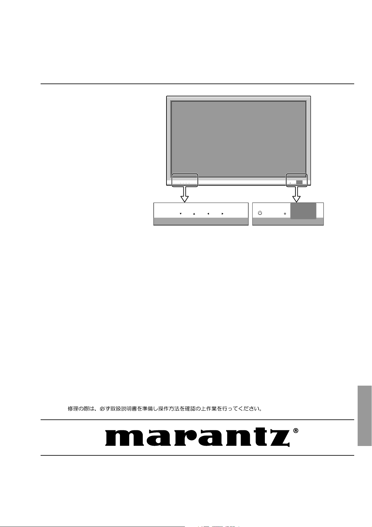
MENU INPUT/EXITVOLUME
TABLE OF CONTENTS
SECTION PAGE
1. TECHNICAL SPECIFICATIONS ....................................... 1
2. SAFETY INFORMATION .................................................. 2
3. FAILURE DIAGNOSIS ................................................... 20
3.1 FAILURE DIAGNOSIS .............................................................. 20
3.2 FAILURE DIAGNOSIS BY LED ............................................... 70
3.3 RS-232C COMMANDS ............................................................ 75
3.4 POWER ON /OFF FUNCTION FOR THE LARGE-SIGNAL
SYSTEM ................................................................................... 82
3.5 FAN CONTROL ........................................................................ 83
4. ADJUSTMENT .............................................................. 84
4.1 ADJUSTMENT REQUIRED WHEN THE SET IS REPAIRED
OR REPLACED ........................................................................ 84
4.2 ADJUSTMENT ......................................................................... 86
4.3 BACKUP OF THE EEPROM (DIGITAL ASSY) ..................... 110
4.4 ADJUSTMENTS WHEN THE SERVICE PANEL ASSY IS
REPLACED ............................................................................. 114
4.5 HOW TO CLEAR HISTORY DATA ........................................ 123
4.6 HOW TO BACKUP EEPROM MEMORY (MAIN ASSY) ....... 124
4.7 MENU INFORMATION ........................................................... 127
5. DISASSEMBLY ............................................................ 140
5.1 PCB LOCATION ..................................................................... 140
5.2 DISASSEMBLY ....................................................................... 141
Plasma Monitor
VOLUME
INPUT/EXIT
MENU
ON/STANDBY
SECTION PAGE
6. EXPLODED VIEWS AND PARTS LIST ....................... 154
6.1 PACKING SECTION ............................................................... 154
6.2 EXTERIOR SECTION ............................................................ 155
6.3 FRONT SECTION .................................................................. 156
6.4 CHASSIS SECTION (1/2 ) ...................................................... 157
6.5 CHASSIS SECTION (2/2) ..................................................... 158
6.6 PANEL CHASSIS SECTION .................................................. 159
6.7 MULTI BASE SECTION ......................................................... 160
6.8 PDP SERVICE ASSY 607MX (AWU1231) ............................. 161
6.9 PARTS LIST ........................................................................... 162
7. BLOCK DIAGRAM ....................................................... 178
7.1 OVERALL CONNECTION DIAGR AM .................................... 178
7.2 CONNECTION PIN EXPLANATION ...................................... 180
7.3 GENERAL BLOCK DIAGRAM ............................................... 202
7.4 MAIN BLOCK DIAGRAM ......................................................... 204
7.5 SUB BLOCK DIAGRAM ......................................................... 205
7.6 DD ASSY ................................................................................ 207
7.7 LVDS ASSY ............................................................................ 208
7.8 PDP MODULE BLOCK DIAGRAM .......................................... 209
7.9 60 ADDRESS L and S ASSYS ............................................... 210
7.10 607 SCAN A and B ASSYS .................................................. 211
7.11 60 X DRIVE ASSY ................................................................ 212
7.12 60 Y DRIVE ASSY ................................................................ 214
7.13 60 DIGITAL ASSY ................................................................. 216
7.14 POWER ON SEQUENCE ..................................................... 217
7.15 IC ........................................................................................... 218
ON/STANDBY
Please use this service manual with referring to the user guide ( D.F.U. ) without fail.
PD6001
Part no. 90M26AV855020
First Issue 2006.12
MZ
Page 2
MARANTZ DESIGN AND SERVICE
Using superior design and selected high grade components,
Only original
MARANTZ
parts can insure that your
MARANTZ
MARANTZ
product will continue to perform to the specifi cations for which
company has created the ultimate in stereo sound.
it is famous.
Parts for your
MARANTZ
ORDERING PARTS :
equipment are generally available to our National Marantz Subsidiary or Agent.
Parts can be ordered either by mail or by Fax.. In both cases, the correct part number has to be specifi ed.
The following information must be supplied to eliminate delays in processing your order :
1. Complete address
2. Complete part numbers and quantities required
3. Description of parts
4. Model number for which part is required
5. Way of shipment
6. Signature : any order form or Fax. must be signed, otherwise such part order will be considered as null and void.
USA
MARANTZ AMERICA, INC
100 CORPORATE DRIVE
MAHWAH, NEW JERSEY 07430
USA
AUSTRALIA
QualiFi Pty Ltd,
24 LIONEL ROAD,
MT. WAVERLEY VIC 3149
AUSTRALIA
PHONE : +61 - (0)3 - 9543 - 1522
FAX : +61 - (0)3 - 9543 - 3677
EUROPE / TRADING
MARANTZ EUROPE B.V.
P. O. BOX 8744, BUILDING SILVERPOINT
BEEMDSTRAAT 11, 5653 MA EINDHOVEN
THE NETHERLANDS
PHONE : +31 - 40 - 2507844
FAX : +31 - 40 - 2507860
THAILAND
MRZ STANDARD CO., LTD
746 - 754 MAHACHAI ROAD.,
WANGBURAPAPIROM, PHRANAKORN,
BANGKOK, 10200 THAILAND
PHONE : +66 - 2 - 222 9181
FAX : +66 - 2 - 224 6795
CANADA
MARANTZ CANADA INC.
5-505 APPLE CREEK BLVD.
MARKHAM, ONTARIO L3R 5B1
CANADA
PHONE : 905 - 415 - 9292
FAX : 905 - 475 - 4159
SINGAPORE
WO KEE HONG DISTRIBUTION PTE LTD
No.1 JALAN KILANG TIMOR
#08-03 PACIFIC TECH CENTRE
SINGAPORE 159303
PHONE : +65 6376 0338
FAX : +65 6376 0166
NEW ZEALAND
WILDASH AUDIO SYSTEMS NZ
14 MALVERN ROAD MT ALBERT
AUCKLAND NEW ZEALAND
PHONE : +64-9-8451958
FAX :+64-9-8463554
JAPAN
D&M Holdings Inc.
D&M BUILDING, 2-1 NISSHIN-CHO,
KAWASAKI-KU, KAWASAKI-SHI,
KANAGAWA, 210-8569 JAPAN
TAIWAN
PAI- YUING CO., LTD.
6 TH FL NO, 148 SUNG KIANG ROAD,
TAIPEI, 10429, TAIWAN R.O.C.
PHONE : +886 - 2 - 25221304
FAX : +886 - 2 - 25630415
MALAYSIA
WO KEE HONG ELECTRONICS SDN. BHD.
2ND FLOOR BANGUNAN INFINITE CENTRE
LOT 1, JALAN 13/6, 46200 PETALING JAYA
SELANGOR DARUL EHSAN, MALAYSIA
PHONE : +60 - 3 - 7954 8088
FAX :+60-3-79547088
KOREA
MARANTZ KOREA CO., LTD.
ROOM 604, ELECTRO OFFICE, 16-58,
HANGGANG-RO 3GA, YONGSAN-KU,
SEOUL, 140-013, KOREA
PHONE : +82 - 2 - 323 - 2155
FAX : +82 - 2 - 323 - 2154
CHINA
MARANTZ SHANGHAI TRADING LTD.
ROOM.506 SHANGHAI LIGHT INDUSTRY MANSION
1578 NANJING (WEST) ROAD SHANGHAI
CHINA
TEL : 021 - 6248 - 1064
FAX : 021 - 6248 - 3565
SHOCK, FIRE HAZARD SERVICE TEST :
CAUTION : After servicing this appliance and prior to returning to customer, measure the resistance between either primary AC
cord connector pins ( with unit NOT connected to AC mains and its Power switch ON ), and the face or Front Panel of product and
controls and chassis bottom.
Any resistance measurement less than 1 Megohms should cause unit to be repaired or corrected before AC power is applied, and
verifi ed before it is return to the user/customer.
Ref. UL Standard No. 60065.
In case of diffi culties, do not hesitate to contact the Technical
Department at above mentioned address.
060607MZ
Page 3
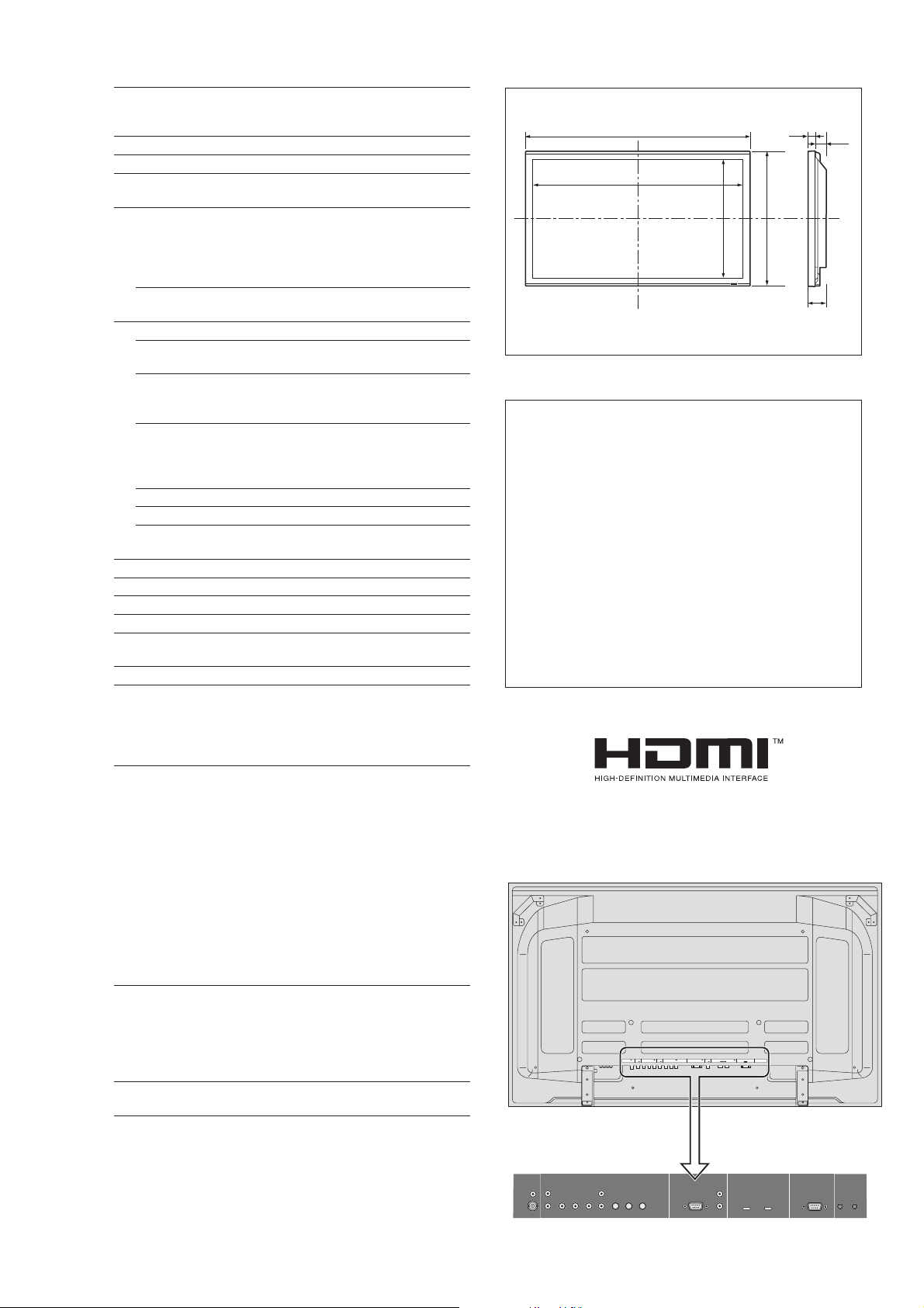
1. TECHNICAL SPECIFICATIONS
Screen Size 51.9 inches(H)⳯29.2 inches(V)
1319 mm(H)⳯742 mm(V)
diagonal 60 inches
Aspect Ratio 16 : 9
Resolution 1365 pixels(H)⳯768 pixels(V)
Pixel Pitch 0.038 inches(H)⳯0.038 inches(V)
0.97 mm(H)⳯0.97 mm(V)
Signals
Synchronization Range Horizontal : 15.5 kHz to 110.0 kHz
(automatic : step scan)
Vertical : 50.0 Hz to 120.0 Hz
(automatic : step scan)
Input Signals RGB, NTSC (3.58/4.43), PAL (B,G,M,N),
PAL60, SECAM, HD*
1
, DVD*
1
Input Terminals
PC/RGB
Visual 1 (Analog) mini D-sub 15-pin⳯1
Video
Visual 1 RCA⳯1
Visual 2 S-Video: DIN 4-pin⳯1
DVD/HD
Visual 1 RCA-pin (Y, Cb/Pb, Cr/Pr)⳯1*
Visual 2 RCA-pin (Y, Cb/Pb, Cr/Pr)⳯1*
HDMI HDMI connector⳯2*
2
1
1
Audio Stereo RCA⳯3 (Selectable)
External Control D-sub 9-pin⳯1 (RS-232C)
Remote In Mini jack⳯1
Remote Out Mini jack⳯1
Sound output 9 W+9 W at 6 ohm
Power Supply AC100 V to 240 V 50 Hz/60 Hz
Current Rating 7.0 A (maximum)
Power Consumption 440 W (typical)
Dimensions 58.1 inches(W)⳯34.7 inches(H)⳯5.0 inches(D)
1476 mm(W)⳯880 mm(H)⳯126 mm(D)
Weight 135.6 lbs / 61.5 kg (without stand)
Environmental Considerations
Operating Temperature 0 °C to 40 °C / 32 °F to 104 °F
Humidity 20 % to 80 % (no condensation)
Storage Temperature -10 °C to 50 °C / 14 °F to 122 °F
Humidity 10 % to 90 % (no condensation)
Other Features Motion compensated 3D Scan Converter (NTSC,
PAL, 480I, 576I, 525I, 625I, 1035I, 1080I), 2-3
pull down Converter (NTSC, 480I, 525I, 1035I,
1080I (60 Hz)), 2-2 pull down Converter (PAL,
576I, 625I, NTSC, 480I, 525I), Digital Zooming
(100 % to 900 % Selectable), Self Diagnosis via
RS232C, PDP Saver (PEAK BRIGHT,
ORBITER, INVERSE, WHITE, SCREEN
WIPER, SOFT FOCUS, etc.), Color Temperature
Select (high/middle/middle low/low, user has 4
memories), Auto Picture Adjust, Input Skip, Color
Tune, Gamma Correction (4 modes), Plug and
play (DDC1, DDC2b, HDMI: E-DDC),
Enhanced Split Screen, etc.
Accessories Power cord (⳯1), Remote control (⳯1), AAA
batteries (⳯2), Manuals (User guide), Ferrite
cores for power cord (⳯2), bands for power
code (⳯2), Cable clampers (⳯3), beads bands
(⳯3), Ferrite core for remote cable (⳯2),
Warranty card
Regulations UL 60065, CAN/CSA-C22.2 No.60065-03,
FCC class B, ICES-003 class B
1.9"
3.0"
58.1" (1476)
(49)
(77)
51.9" (1319)
34.7" (880)
29.2" (742)
5.0"
(126)
Units are in inch
(mm)
The features and specifications may be subject to change without
notice.
*1DVD/HD input signals supported on this system.
480P (60 Hz) 480I (60 Hz) 525P (60 Hz)
525I (60 Hz) 576P (50 Hz) 576I (50 Hz)
625P (50 Hz) 625I (50 Hz) 720P (60 Hz)
720P (50 Hz) 1035I (60 Hz) 1080I (50 Hz)
1080I (60 Hz) 1080P (50 Hz) 1080P (60 Hz)
2
*
HDMI input signals supported on this system.
Supported Signals
• 640ⴒ480P @ 59.94/60 Hz • 1920ⴒ1080I @ 50 Hz
• 1280ⴒ720P @ 59.94/60 Hz • 720ⴒ576P @ 50 Hz
• 1920ⴒ1080I @ 59.94/60 Hz • 1440 (720)ⴒ576I @ 50 Hz
• 720ⴒ480P @ 59.94/60 Hz • 1280ⴒ720P @ 50 Hz
• 1440 (720)ⴒ480I @ 59.94/60 Hz
Note: In some cases a signal on the plasma monitor may not be displayed
properly. The problem may be an inconsistency with standards from
the source equipment (DVD, Set-top box, etc...). If you do experience
such a problem please contact Marantz America, Inc. and also the
manufacturer of the source equipment.
HDMI, the HDMI logo and High-Definition Multimedia Interface are
trademarks or registered trademarks of HDMI Licensing LLC.
DVD/HD3DVD/HD
VIDEO AUDIO
1
AUDIO
DVD/HD1DVD/HD
Cb/Pb Cr/Pr L/R Y Cb/Pb Cr/PrL/R Y
2
2
4
AUDIO
3
PC/RGB
L/R
REMOTE
EXTERNALCONTROL
IN OUT
DVD/HD3DVD/HD
VIDEO AUDIO
1
2
R
(
MONO
L
1
YCb/PbCr/Pr
)
2
AUDIO
DVD/HD
1
DVD/HD
2
R
YCb/PbCr/Pr
(
)
L
MONO
AUDIO
3
PC/RGB
R
(
)
MONO
L
4
HDMI
HDMI
EXTERNALCONTROL
REMOTE
IN
OUT
1
Page 4

2. SAFETY INFORMATION
SAFETY INFORMATION
This service manual is intended for qualified service technicians ; it is not meant for the casual
do-it-yourselfer. Qualified technicians have the necessary test equipment and tools, and have been
trained to properly and safely repair complex products such as those covered by this manual.
Improperly performed repairs can adversely affect the safety and reliability of the product and may
void the warranty. If you are not qualified to perform the repair of this product properly and safely,
you should not risk trying to do so and refer the repair to a qualified service technician.
WARNING
This product contains lead in solder and certain electrical parts contain chemicals which are known to the state of California to
cause cancer, birth defects or other reproductive harm.
NOTICE
(FOR CANADIAN MODEL ONLY)
Fuse symbols (fast operating fuse) and/or (slow operating fuse) on PCB indicate that replacement parts
must be of identical designation.
REMARQUE
(POUR MODÈLE CANADIEN SEULEMENT)
Les symboles de fusible (fusible de
de remplacement doivent avoir la même désignation.
type rapide) et/ou (fusible de type lent) sur CCI indiquent que les pièces
Health & Safety Code Section 25249.6 - Proposition 65
SAFETY PRECAUTIONS
NOTICE : Comply with all cautions and safety related notes
located on or inside the cabinet and on the chassis.
The following precautions should be observed :
1. When service is required, even though the PDP UNIT an
isolation transformer should be inserted between the power line
and the set in safety before any service is performed.
2. When replacing a chassis in the set, all the protective devices
must be put back in place, such as barriers, nonmetallic knobs,
adjustment and compartment covershields, isolation resistorcapacitor, etc.
3. When service is required, observe the original lead dress. Extra
precaution should be taken to assure correct lead dress in the
high voltage circuitry area.
4. Always use the manufacture's replacement components.
Especially critical components as indicated on the circuit
diagram should not be replaced by other manufacture's.
Furthermore where a short circuit has occurred, replace those
components that indicate evidence of overheating.
5. Before returning a serviced set to the customer, the service
technician must thoroughly test the unit to be certain that it is
completely safe to operate without danger of electrical shock,
and be sure that no protective device built into the set by the
manufacture has become defective, or inadvertently defeated
during servicing. Therefore, the following checks should be
performed for the continued protection of the customer and
servicetechnician.
6. Perform the following precautions against unwanted radiation
and rise in internal temperature.
• Always return the internal wiring to the original styling.
• Attach parts (Gascket, Ferrite Core, Ground, Rear Cover,
Shield Case etc.) surely after disassembly.
7. Perform the following precautions for the PDP panel.
• When the front case is removed, make sure nothing hits the
panel face, panel corner, and panel edge (so that the glass does
not break).
• Make sure that the panel vent does not break. (Check that the
cover is attached.)
• Handle the FPC connected to the panel carefully.
Twisting or pulling the FPC when connecting it to the
connector will cause it to peel off from the panel.
8. Pay attention to the following.
• Pay extreme caution when the front case and rear panel are
removed because this may cause a high risk of disturbance to
TVs and radios in the surrounding.
2
Page 5
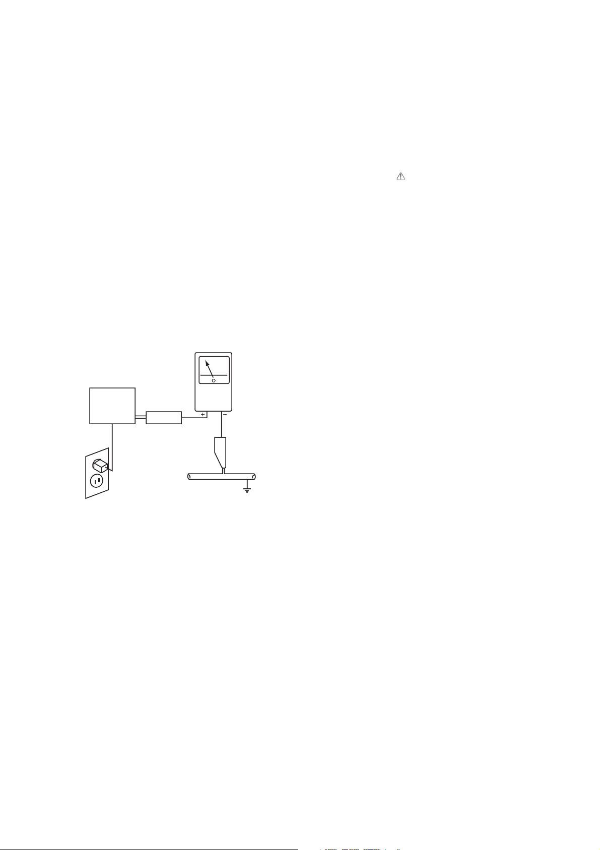
Insulation Resistance Check
With the AC plug removed from an AC power source, place a
jumper across the two plug prongs. Turn the AC power switch on.
( Case of PD6001, AC power is alwayas on. )
(Case of PX-60XR5A, AC power is always on.)
Using an insulation tester (DC 500V), connect one lead to the
jumpered AC plug and touch the other lead to each exposed metal
part (input/output terminals, screwheads, metal overlays, control
shafts, etc.), The resistance should be greater than 4 MΩ.
Leakage Current Hot Check
Plug the AC line cord directly into an AC power source (do not
use an isolation transformer for this check).
Turn the AC power switch on.
Using a "Leakage Current Tester", measure for current from all
exposed metal parts of the cabinet (input/output terminals,
screwheads, metal overlays, control shaft, etc.), particularly any
exposed metal part having a return path to the chassis, to a known
earth ground (water pipe, etc.). Any current measured must not
exceed 1.0 mA.
PRODUCT SAFETY NOTICE
Many electrical and mechanical parts in the Set have special
Many electrical and mechanical parts in PIONEER set have
safety related characteristics. These are often not evident
special safety related characteristics. These are often not evident
from visual inspection nor the protection afforded by them
from visual inspection nor the protection afforded by them
necessarily can be obtained by using replacement components
necessarily can be obtained by using replacement components
rated for higher voltage, wattage, etc. Replacement parts which
rated for higher voltage, wattage, etc. Replacement parts which
have these special safety characteristics are identified in this
have these special safety characteristics are identified in this
Service Manual.
Service Manual.
Electrical components having such features are identified by
marking with a on the schematics and on the parts list in this
Service Manual.
The use of a substitute replacement component which dose not
have the same safety characteristics as the PIONEER
recommended replacement one, shown in the parts list in this
Service Manual, may create shock, fire or other hazards.
Product Safety is continuously under review and new instructions
are issued from time to time. For the latest information, always
consult the current PIONEER Service Manual. A subscription to,
or additional copies of, PIONEER Service Manual may be
obtained at a nominal charge from PIONEER.
Reading should
not be above
1.0 mA
Earth
ground
Device
under
test
Also test with
plug reversed
(Using AC adapter
plug as required)
Leakage
current
tester
Test all
exposed metal
surfaces
AC Leakage Test
ANY MEASUREMENTS NOT WITHIN THE LIMITS
OUTLINED ABOVE ARE INDICATIVE OF A POTENTIAL
SHOCK HAZARD AND MUST BE CORRECTED BEFORE
RETURNING THE SET TO THE CUSTOMER.
3
Page 6
Safety cautions
The matters to be observed without fail are explained below. These matters are indispensable for the
prevention of an accident during the maintenance servicing, the "security of products" after the completion of
servicing work, and the "prevention of the repeated occurrence of similar fault."
(1) The degree of danger and material damage, caused as a result of wrong use by disregarding the contents
of the display" is distinguished and explained in the table below.
If this display is disregarded and equipment is handled
WARNING
CAUTION
(2) Kinds of the matters to be observed are classified and explained in the icons shown below.
This icon indicates a dangerous place where an electric shock is anticipated.
This icon indicates the contents of "caution" that must be borne in mind, without fail.
wrongly, this can be a cause of physical injury and a
fire, thus leading a person to death or serious injury.
If this display is disregarded and equipment is
handled wrongly, this may lead to personal injury or
material damage.
This icon indicates the contents of "caution" that must be practiced, without fail.
WARNING
• Observe the caution matter, without fail.
• In the place where a particular caution is needed during maintenance servicing, such a
caution note is displayed with a label or a stamp that is given to the cabinet, chassis,
PWB, etc. These caution notes and also the caution matters of given in
the instruction manuals, etc., must be observed, without fail.
• Be careful of an electric shock or a burn.
• The power block or the PDP module involves the sections where high voltage or high
temperature is prevalent. When equipment is energized, use working gloves in order to
prevent an electric shock or a burn. At the time of transportation, disassembly,
reassembly, and the replacement of parts, such a servicing job must be done after pulling
out the power plug.
• Modification of equipment is absolutely prohibited. Use the specified parts at all times.
• If any modification is performed, the validity of the manufacturer's warranty is lost at that
moment. The personnel who did this modification is responsible for the physical injury or
the like, if it should occur as a result of the modification. The parts used are given the
safety-based characteristics, such as non-flammability or sufficient withstand voltage. The
parts to be replaced shall be those which are specified in the list of replacement
parts.(Example: The lithium battery (circuit symbol BT9501 in the MAIN PWB) will give
rise to explosion if its polarity is wrongly treated.
WARNING
• The replaced parts and wiring must be arranged in the original conditions.
• For safety reasons, insulation materials like tubes and tapes may be used or some parts
may be mounted clear of the PWB. The internal wiring and the fastening with the
clampers for separation from high-heat and high-voltage parts shall be returned to their
original conditions, without fail.
4
Page 7
CAUTION
• Observe the caution matter, without fail
The caution matters of given in the instruction manuals, etc., must be
•
observed, without fail.
• Do not give shocks and vibration.
The panel surface (display plane) of the filter and the PDP module (include the PDP
•
Service ASSY)
and the scattered glass chips will be a cause of injury.
• Do not put anything.
Do not put anything on the product. Otherwise, this can be a cause of injury as a result
•
of falling down or dropping caused by imbalance.
• Transportation must be done by enough personnel.
The product is heavy. In the case of transportation, unpacking, or packing, more than
•
two persons should do it (three persons for a product of 60-inch or larger) by supporting
the top and the bottom of the product.
is made of glass. If any shocks or vibration is applied, it may be broken
CAUTION
Miscellaneous caution matters
(1) This product uses highly integrated semiconductor parts. Since these parts are fragile to
electrostatic charges, earth bands should be used for handling. The product should be handled
where measures have been taken against electrostatic charges.
(2) If this product is used for the fixed character display or the like as in the case of a character
display board, a phenomenon of burning (not warranted) will occur. Burning is a phenomenon
that the unevenness in the brightness is caused in the display. In such a case, the brightness in
the section where the integrated display time is longer becomes lower than the brightness in
another section where the integrated display time is shorter. This phenomenon is in proportion
to the integrated display time and the brightness. For this reason, to relieve this difficulty during
servicing, do not use any still picture, but use a display by motion pictures of a video or the like.
In addition, use "FULL" for the screen mode and avoid using any display by "NORMAL",
"TRUE", or MULTI SCREEN like side by side etc. If it is necessary to use only a still picture for
unavoidable reasons, use a burning relief function such as "PLE LOCK", "ORBITER",
"SCREEN WIPER", etc.
(3) When a PDP module (include the PDP Service ASSY) is operated after a long time of storage,
it may encounter a difficulty like a failure in displaying a screen or unstability according to the
condition of storage. In such a case, the PDP module (include the PDP Service ASSY) should
be incorporated in the product and aging treatment should be carried out for about two hours
(all screen display).
(4) Sulfides will deteriorate the PDP module (include the PDP Service ASSY) and this is a cause of
malfunction. Therefore, it is absolutely prohibited to put any vulcanized rubber or a material
containing sulfur in the vicinity of the PDP module (include the PDP Service ASSY).
(5) When taking out a PDP module (include the PDP Service ASSY) from the maintenance
5
Page 8

package box, do it slowly so that the panel surface does not get any shock or stress.
If one touches the connector of the flexible cable exposed to the rear side of the PDP module
(6)
(include the PDP Service ASSY), there is danger of causing a poor contact. As such, it must be
handled with utmost care. In addition, the flexible cable is very weak in mechanical strength.
Therefore, this cable must not be touched during handling.
(7) The panel surface of the filter and the PDP module (include the PDP Service ASSY) is easy to
be hurt. These components should be handled very carefully not to press or rub them with a
hard thing. Never put them on a hard thing with the panel surface faced downwards.
When the panel surface of the filter and the PDP module (include the PDP Service ASSY) is
(8)
contaminated, gently wipe off the contaminant with a piece of soft dry cloth. Liquid-state
contamination can be removed by lightly pressing it, without rubbing it. If it is difficult to remove
the contamination, use a piece of cloth soaked with a neutral detergent
water.)
or a rubbing alcohol. The cloth for wiping off should be clean. Never use the same cloth
(Use it, diluting with
repeatedly. If a cleansing detergent or water drops should enter the module interior or be
attached to the module surface other than the display plane at the time of cleaning, this will give
rise to the destruction of the product when the product is energized.
(9) When transporting this product, use the packing materials specified in the list of parts. Once
used, such packing materials should not be used again.
(10) This product is composed of a variety of parts, such as those made of materials like glass,
metal, plastics, etc., and those like a lithium battery (circuit symbol of the MAIN ASSY: BT9501),
etc. Therefore, when abandoning this product, this should be done in accordance with the
relevant law of the nation or an autonomous body.
CAUTION: Risk of Explosion if Battery is replaced by an Incorrect Type. Dispose of Used
Batteries According to above the Instructions.
(11) You should use the following service tools when you replace ICs etc. since solder with free lead is
used in product.
∗ Soldering iron for solder with free lead ; HAKKO SOLDERING IRON 934 (Hakko corporation)
(See the following web address in detail. http://realwww.hkk.idanet.ne.jp/english/index.html)
∗ Solder with free lead ; SN96C 0.3 mm (NIHON SUPERIOR CO., LTD)
(See the following web address in detail. http://www.nihonsuperior.co.jp/english/index.html)
6
Page 9
Charged Section
High Voltage Generating Point
The places where the commercial AC power is used without
passing through the power supply transformer.
If the places are touched, there is a risk of electric shock. In
addition, the measuring equipment can be damaged if it is
connected to the GND of the charged section and the GND of the
non-charged section while connecting the set directly to the
commercial AC power supply. Therefore, be sure to connect the
set via an insulated transformer and supply the current.
1. Power cord
2. AC inlet
3. Power switch (S1)
4. Fuse (In the POWER SUPPLY Unit)
5. STB transformer and Converter transformer
(In the POWER SUPPLY Unit)
6. Other primary side of the POWER SUPPLY Unit
: Part is Charged Section.
: Part is the High Voltage Generating Points
other than the Charged Section.
607 SCAN B Assy
60 Y DRIVE Assy
The places where voltage is 100 V or more except for the charged
places described above. If the places are touched, there is a risk of
electric shock.
The VSUS voltage remains for several minutes after the power to
the unit is turned off. These places must not be touched until
about 10 minutes after the power is turned off, or it is confirmed
with a tester that there is no residual VSUS voltage.
If the procedures described in “3.4 POWER ON/OFF FUNC-
-TION FOR THE LARGE-SIGNAL SYSTEM” are performed
before the power is turned off, the voltage will be discharged in
about 30 seconds.
POWER SUPPLY Unit..................................................(DC205 V)
60 X DRIVE Assy...............................................(–180 V to 205 V)
60 Y DRIVE Assy..............................................(–500 V to 500 V)
607 SCAN A Assy..............................................(–500 V to 500 V)
607 SCAN B Assy..............................................(–500 V to 500 V)
60 X DRIVE Assy Conductive plate XPOWER SUPPLY Unit
607 SCAN A Assy
Power switch (S1)
AC inlet
Fig. High Voltage Generating Point (Rear view)
7
Page 10
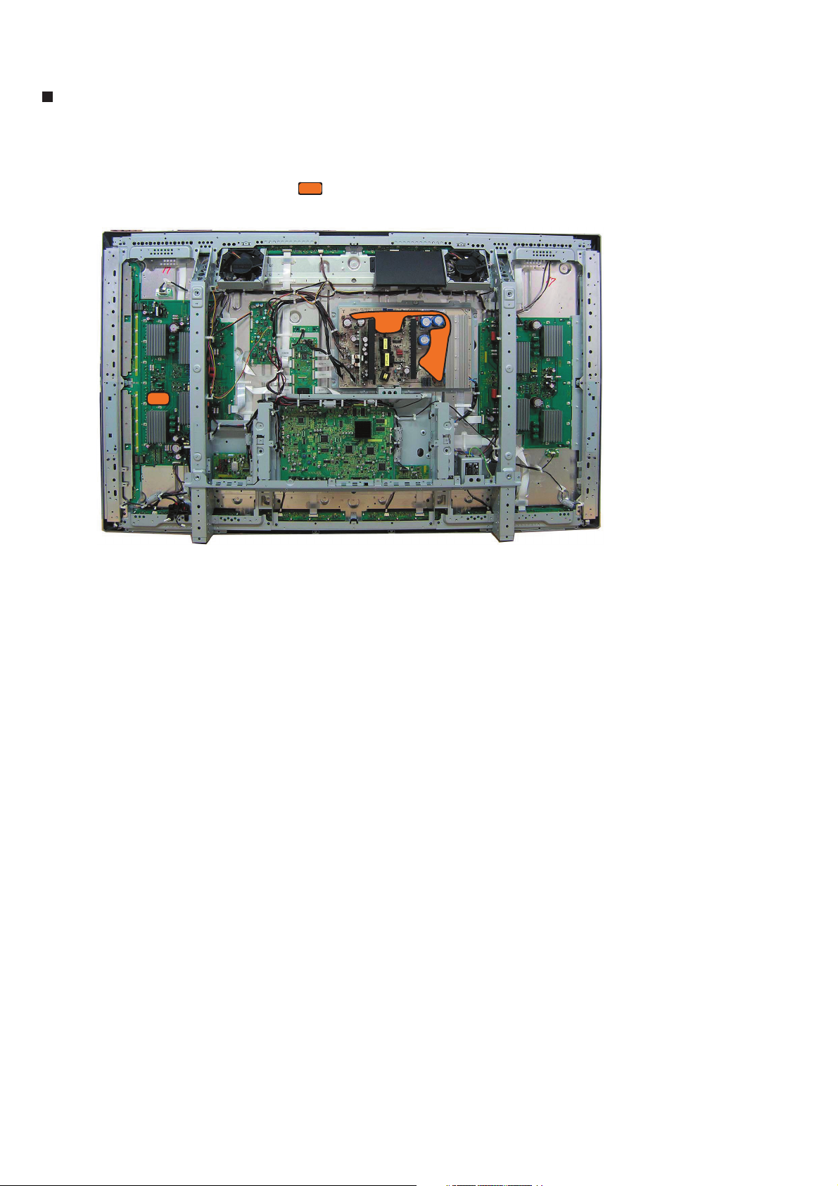
High Temperature Section
Caution: Because the places circled ( ) in the photo can be extremely hot, work with care.
8
Page 11
[Important Check Points for Good Servicing]
In this manual, procedures that must be performed during repairs are marked with the below symbol.
Please be sure to confirm and follow these procedures.
1. Product safety
Please conform to product regulations (such as safety and radiation regulations), and maintain a safe servicing environment by
following the safety instructions described in this manual.
1 Use specified parts for repair.
Use genuine parts. Be sure to use important parts for safety.
2 Do not perform modifications without proper instructions.
Please follow the specified safety methods when modification(addition/change of parts) is required due to interferences such as
radio/TV interference and foreign noise.
3 Make sure the soldering of repaired locations is properly performed.
When you solder while repairing, please be sure that there are no cold solder and other debris.
Soldering should be finished with the proper quantity. (Refer to the example)
4 Make sure the screws are tightly fastened.
Please be sure that all screws are fastened, and that there are no loose screws.
5 Make sure each connectors are correctly inserted.
Please be sure that all connectors are inserted, and that there are no imperfect insertion.
6 Make sure the wiring cables are set to their original state.
Please replace the wiring and cables to the original state after repairs.
In addition, be sure that there are no pinched wires, etc.
7 Make sure screws and soldering scraps do not remain inside the product.
Please check that neither solder debris nor screws remain inside the product.
8 There should be no semi-broken wires, scratches, melting, etc. on the coating of the power cord.
Damaged power cords may lead to fire accidents, so please be sure that there are no damages.
If you find a damaged power cord, please exchange it with a suitable one.
9 There should be no spark traces or similar marks on the power plug.
When spark traces or similar marks are found on the power supply plug, please check the connection and advise on secure
connections and suitable usage. Please exchange the power cord if necessary.
0 Safe environment should be secured during servicing.
When you perform repairs, please pay attention to static electricity, furniture, household articles, etc. in order to prevent injuries.
Please pay attention to your surroundings and repair safely.
2. Adjustments
To keep the original performance of the products, optimum adjustments and confirmation of characteristics within specification.
Adjustments should be performed in accordance with the procedures/instructions described in this manual.
3. Lubricants, Glues, and Replacement parts
Use grease and adhesives that are equal to the specified substance.
Make sure the proper amount is applied.
4. Cleaning
For parts that require cleaning, such as optical pickups, tape deck heads, lenses and mirrors used in projection monitors, proper
cleaning should be performed to restore their performances.
5. Shipping mode and Shipping screws
To protect products from damages or failures during transit, the shipping mode should be set or the shipping screws should be
installed before shipment. Please be sure to follow this method especially if it is specified in this manual.
9
Page 12
3. FAILURE DIAGNOSIS
3.1 FAILURE DIAGNOSIS
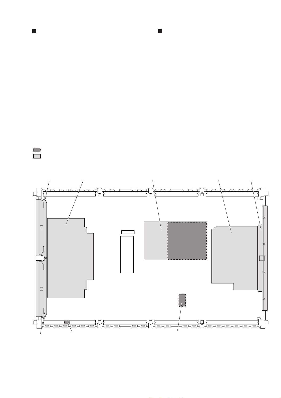
Diagnosis Points of PCB Assy
Note:
If symptoms persist after replacement of parts, such as ICs, following the diagnosis results of this failure-analysis chart, it is
recommended to replace the whole PC board, as short-circuiting or breaking of printed wiring of board patterns is suspected.
MAIN ASSY (XR model)
CN9501
CN9005
CN9004
CN9003
CN9008
CN9001
IC9504
T10
IC9504
CN9001
T31
44 45
15
4
IC5605
IC5302
6
5
3
IC9501
10 12
IC5605
T10
IC5302
T35
45 49
IC5301
IC5301
T11
CN9006
23
IC6201
IC5602
CN8501
IC8501
T22
IC8501
38
PN1
T22
PN2
T22
IC8002
IC8002
T22
39
24
IC8003
T22
X8001
X8002
40
X8001
T22
X8002
T22
CN9010
T40
CN9010
IC6403
T13
2
25
IC5903
T11
T20
13 37
IC5903
IC6501
IC5904
T11
14
11
IC6701
IC7002
IC7004
T21
35
IC7001
CN9009
IC7001
T35
IC5902
T11
IC7003
IC7003
936
8
48
T35
• Legend symbol
45
: Waveform No. on Flowchart.
IC5002
: Broken circuit number on Flowchart, and number of Flowchart that broken parts are written.
T13
20
IC7002
T35
46 47
32
34 33
Page 13
Pin4 of IC5006
Pin10 of IC5006
Pin4 of IC5004
Pin10 of IC5004
Pin7 of IC5902
Pin9 of IC5902
Pin6 of IC5906
No. 8 (IC5006) No. 8 (IC5004) No. 9 and ∞ and º No. !
Pin3 of IC5906
Pin74 of IC6201
Pin73 of IC6201
Pin41,43 of IC3002
Pin47,48 of IC3002
Pin3 of IC9504Pin6 of IC9504
Pin4 of IC5004
Pin3 of IC5005
Pin6 of IC5005
Pin119 of IC6201
No. @ No. & No. * No. )
Pin12 of IC8501
Pin57 of IC8501
Pin55 of IC8501
Pin58 of IC8501
Pin48 of IC7001
Pin121 of IC7001
Pin47 of IC7001 Pin44 of IC7001
No. _ No. ¢ No. ª No. ≠
Pin11 of IC7002
Pin55 of IC101
Pin57 of IC101
No. ‹ No. ‚ No. ± No. [
21
Page 14
SUB ASSY
CN3004
T30
T33
IC3001
CN3004
44
CN3003
CN3003
T31
13
IC3001
T31
IC3002
T30
T31
IC3004
IC3004
T31
L3005
T31
IC3002
41
CN3001
12
CN1101
CN1001
U2102
T41
CN2101
U2102
IC2002 IC2004
IC2004
IC2002
T40
T40
CN2002
JA2002
T40
JA2002
JA2001
T41
JA2001
CN1201
• Legend symbol
45
: Waveform No. on Flowchart.
IC5002
: Broken circuit number on Flowchart, and number of Flowchart that broken parts are written.
T13
22
Page 15
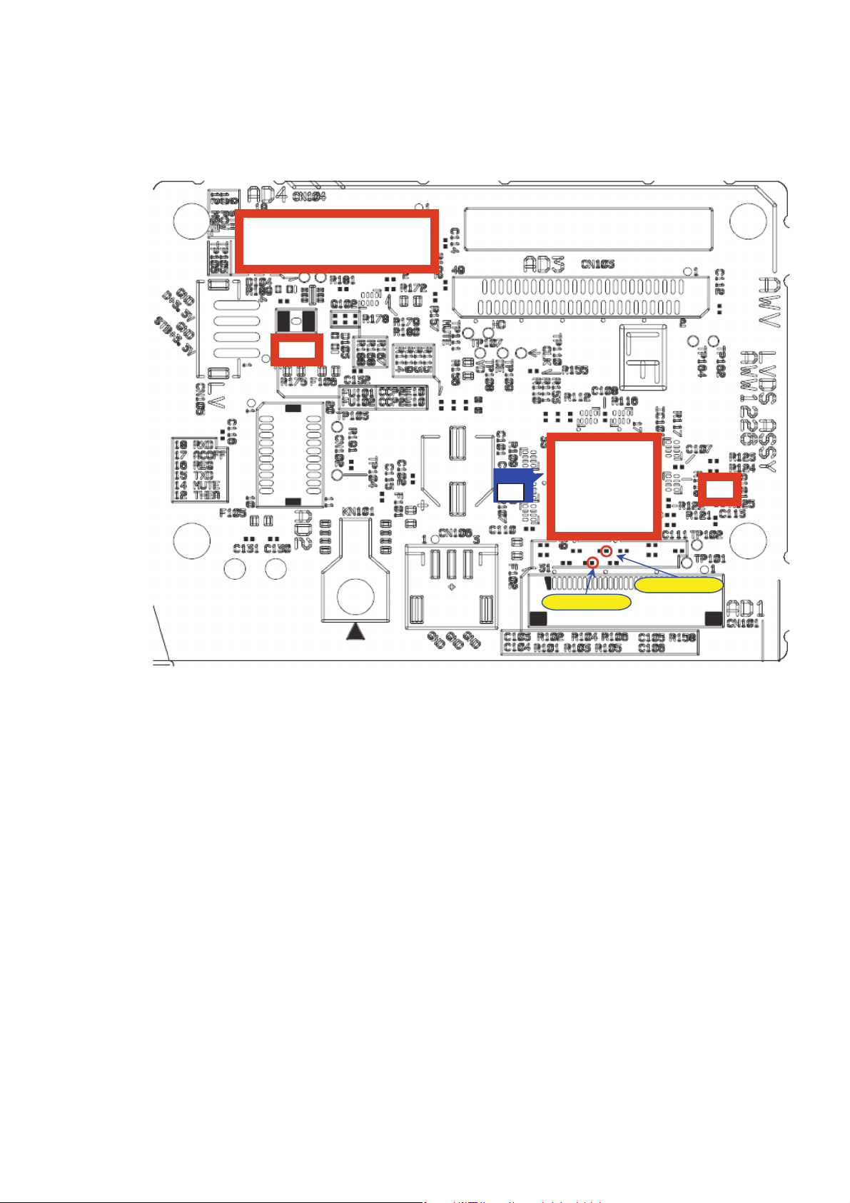
LVDS ASSY
CN104
FU102
IC101
T50
IC101
waveform50
Q101
waveform51
23
Page 16
DD ASSY
IC306
CN305
T61
D303
T63
IC302
T63
D312
T63
CN307
T62
C320
T62
IC303
T62
CN306
T63
T64
Q302
T62
D304
T62
CN302
T62
T64
Q303
T62
Q301
T61
FU301
T61
IC301
T61
CN304
T61
T64
C302
T61
D302
T61
T64
D306
T60
D301
T61
C327
T60
CN309
T60
C328
T60
C326, C337
T60
CN301
T60
T63
D307
T60
C334
T60
C335
T60
IC305
T60
FU302
T60
52
IC302 SW pin (#3)
(= D303 Cathode terminal)
• Legend symbol
52
: Waveform No. on Flowchart.
CN305
: Broken circuit number on Flowchart, and number of Flowchart that broken parts are written.
T61
54 53
Q303 Drain terminal
(#5 - #8)
55
Q301 Drain terminal
(#5 - #8)
IC305 (#11 - #14)
V OUT pin
24
Page 17
H
To LVDS ASSY
F
G
CN3001
To DD ASSY
B
LED
D2102
POLED2
POLED1,
A
C
E
D
CN2101
CN8501
OSD
CN3003
+12V
IC3004
12V to 9V
AUDIO ASSY
CN8502
+3.3V
IC8501
+3.3V
LVDS
Transmitter
U2102
Control
Remote
LED ASSY
S2601
PUSH SW
PWR ASSY
IC1201
SEND ASSY
IC1101
SENC ASSY
IC1001
SENB ASSY
REMIN1
Receiver
CN9008
+6V
REMIN1,
POLED1,
POLED2
POIN, SW7
+3.3V
SCL, SDA
+3.3V
SCL, SDA
+3.3V
SCL, SDA
CN1001 CN1201CN1101 CN2601 CN2602
+12V
+12V
SW7(power on)
LR-in
CN9009
LED-CTL1
(SDA, SCL)
Temp Sens or
CN9004 CN9005CN9003
D9003
Detect.
ALARM
IC9001
FAN Control
IC9505
u-COM
+7V
IC9503
X9501
CN9006
+7V
Power
7V to 3.3 V
+7V
SW7
IC9502
CN9007
7V to 5V
CN9012
+3.3V
+2.5V
+3.3V
LVDS
IC8502
Receiver
+3.3V
IC8105
DSP Controll
+3.3V
+9V
IC3001
IC8101~81 04
Audio
Controller
CN3004
CN9001
SDRAM
+9V
+12V
Audio
IC3002
Amplifier
DC detect
Mute
SCL,
SDL
Audio Control
(Mute, SCL, SDA, ALM)
L/R Audio Signal
ALM
CN7001
Receiver
RGB3
IC8001
Processor
Digital signal
+3.3V
+2.5V
IC8002
2.5V to 1.5V
+5V
IC7002
Audio DAC
+3.3V
HDMI
IC7001
Receiver
JA7001
JA7002
HDMI
DVD/HD3
DVD/HD4
+3.3V
IC8003
+9V
X8001
X8002
3.3V to 1.5V
+9V
SW
Audio
IC5302
IC7003
Audio amp
X7001
IC7004
3.3V to 1.8V
2RCA
2RCA
JA5005
HDMI
JA5006
AUDIO1
XR Model only
Digital V ideo signal , CLK, Sync
TMDS, LVDS
Digital A udio signal
Analog Audio signal
Power Supply
Analog Video signal
Control s ignal
Sync sig nal
2RCA
JA5007
AUDIO2
AUDIO3
+3.3V
CN2002
CN9011 CN9010 CN9501
REMIN1
+5V
TXD1
REMIN2
RXD0/TXD0
+3.3V
232C
IC2001
Receiver
Control
JA2001
CN2001
External
9p D-sub
232C ASSY
CN2201
CTL1
S2202
S2203
S2201
Tac t S W
Tact SW
CTL ASSY
Logic
IC2004
+5V
+5V
Logic
IC2002
IC2003
5V to 3.3 V
+3.3V
JA2002
Remote
Remote In
Tac t S W
Mini jack
Mini jack
CTL2
S2204
S2205
S2206
Tac t S W
Tac t S W
+6V
IC6204
IC6203
6V to 3.3 V
3.3V to 1 .5V
IC6201
Chroma Decoder
+3.3V
+9V
SW
IC5003
BNC
Tac t S W
JA5001
VIDEO1
MAIN ASSY
IC6202
SDRAM
Loop
IC5002
XM Model
only
X6201
XR Model
A/D
IC6501
Converter
LPF
LPF
IC5601
JA5003
SW
Video
3RCA
DVD/HD
+3.3V
+5V
IC5605
+3.3V
IC5004
5BNC
JA5004
Sync sep
IC5603
Buffer
RGB/DVD2
+5V
IC5602
IC5602
+5V
RCA+S
JA5002
VIDEO2
VIDEO3
VIDEO1, VIDEO2(S)
IC5604
/HD2
Sync SW
SW
+3.3V
XM
+5V
+3.3V
A/D
IC6701
Converter
Buffer
IC9504
+5V
+5V
LPF
IC5905
+5V
SW
Video
IC5901
IC5006
Model
only
Loop
RY5001
RY5002
CN5001
XR Model
PC/RGB
+3.3V
SW
IC5904
Buffer
IC5906
+5V
IC5903
Sync sep
+3.3V
IC5902
Sync SW
Buffer
+7V
15p D-sub
+7V
RGB1
DVI
IC7001
IC7006
7V to 5V
TMDS line
IC7006
7V to 5V
XM Model only
General Block Diagram (1/2)
XR Model : PD5001/PD6001
25
Page 18
LVDS
RECEIVERRECEIVER
DK BLOCKDK BLOCK
IC 1601
60 ADDRESS L
ASSY
AD1
AD2
HOT
60X DRIVE ASSY
X
MASK
MODULE
PLATE
IC1203
X
MASK
MODULE
IC1205
X
DK
MODULE
IC1103
X
DK
MODULE
IC1131
BLOCK
X RESET
60 ADDRESS L
ASSY
AD2AD1
LVDS
DK
BLOCK
RECEIVERRECEIVER
IC 1601
P7
P2
P4
P1 P7 P6P4 P2
LVDS
DK BLOCK
LVDS
DK BLOCK
LVDS
RECEIVER
RECEIVER
IC 1801
60 ADDRESS S
IC 1801
60 ADDRESS S
IC 1601
60 ADDRESS L
ASSY
ASSY
ASSY
+60VP7+60V
+16.5V
IC306
+12 to 7.8V
ALARM
Detect.
AC INLET
P3
CN312CN313
CN315
CN103
To LVDS ASSY
CN104
To LVDS ASSY
P6
P1
P1
Vsus
+6.5V
+16.5V
Power Supply Unit
+16.5V
P12
IC302
+16.5V to 1 2V
DD ASSY
+12V
P2
+16.5V
+12V
+6V
P4
Vsus
+12V
+12V
+6.5V
STB3.3V
EXT_PD
STB3.3V
VSUS_ADJ
M_SW_DET
+6.5V
+12V
+16.5V
+5.1V
P8
CN302(P8)
IC301
IC303
+5.1 to +3. 3V
STB3.3 to +7V
+7V
+3.3V
+2.7V
P6
DRF_B
RELAY
PS_PD
AC DET
PD_TRIG_B
P5
CN(301)CN304(P12)
IC305
+16.5 to + 12V
+12V
AD1
D9
AND
Ext_PD
SQ_SD
SDA
SCL,
DAC
STOP_SQ
SCAN
YSUS
Vofs_ADJ, VYPRST_ADJ
D10
PD
YSUS
&
OVER
Pulse
UNDER
&
OVER
XSUS
PD_MUTE
AND
OR
MASK
Width
YPR-U
DET
VOL
AD2
AD1
AD2
PANEL
SENSOR ASSY
TE1
D21
X3
+12V
Y6
VOLTAGE
CONVERTER
BLOCK
X2X5
DRF
AND
RELAY KDD
Vsus_ADJ
DC-DC
RELAY, PD_TRG_B, AC_DET
V+3V_D
SCL,
SDA
TEMP1
V+3V_EEP
D24
Y4Y5
BLOCK
VOLTAGE
CONVERTER
DRF_B
+12V
PS_PWDN
MODULE
AXY1137-
CONVERTER
V+1V_D
VH_UV_PD, YDRIVE_PD
YRESNC_PD,
YDD_CNV_PD
XSUSTN_PD, XDD_CNV_PD
XDRIVE_PD
IC5V_UV_PD
60Y DRIVE ASSY
VH
DCDC-CON
Y
MASK
MODULE
IC2301
Y
MASK
MODULE
IC2301
Y
MASK
MODULE
IC2302
Y
MASK
MODULE
IC2302
Y
DK
MODULE
IC2103
Y
DK
MODULE
IC2103
Y2
AD2 AD1
VH
SCAN
SCAN
607 SCAN B
ASSY
SCAN
IC2902
IC2901
SCAN
IC2903
CN2902
CN2903
(PSUS)
HOT
PLATE
SCAN
IC2904
SCAN
IC2905
SCAN
IC2906
CN2904
Y
Y
CN2905
UNDER
PD
DRF_B
ADR_PD1
OR
DK
DK
PSUS
VOL
DET
MODULE UCOM
ADR_PD5
MODULE
MODULE
VH
SCAN
SCAN
V+3V_D
XSUS
M30620FCPGP
OR
V+3V_D
IC2151
IC2151
IC2801
CN2802
IC3151
LOGIC
Y SUS MASK
Y SUS -B
BLOCK
Y RESET
Y
Reset
SCAN
IC2802
XSUS MASK
XSUS_U
LOGIC
D18
D17
BLOCK
Y SUS -G
BLOCK
XSUS_D
BLOCK
PHOTO
Y SUS -U
Y SUS -D
Y OFFSET
Y
SCAN
IC2803
XSUS_B
XSUS_G
PHOTO
V+3V_D
V+3V_D
COUPLER
Y PR-U
BLOCK
OFFSET
BLOCK
Y3
CN2801 CN2901
CN2803
XNR-D
COUPLER
X1
D19
&
SUB-FILD CONV.
PATTERN GEN.
XY DRV SEQUENCE
UART
SW
D16
Y1
Y OFS
SCAN CONTROL
PHOTO
COUPLER
SCAN
IC2804
CN2804
LVDS
PEG122C-K
LVDS
V+3V_D
Y8
SCAN
IC2805
IC3401
X6
V+3V_D
D8
H DET
HD
VD
FLASH MEMORY
IC3301
D5
PSUS
SCAN
IC2806
CN2805
AD2AD1
V+3V_D
V+3V_D
AD2AD1
AD2AD1
607 SCAN A
ASSY
BLOCK
DK
LVDS
60 ADDRESS S
ASSY
D7
HD, VD, DCLK, DE
RA, GA, BA
THEATER
LED_R
D6
DK BLOCK
RECEIVER
LVDS
60 ADDRESS S
ASSY
60 ADDRESS L
ASSY
DK BLOCK
RECEIVER
LVDS
IC 1801
60 DIGITAL ASSY
D11
UART
INP_MUTE
V+3VACT
LED_B
MSEL
YOBI
D12
V+3V_D
IC 1801
IC 1601
PDP Module
GF
(1/2)
To MAIN ASSY
CN101 CN102
General Block Diagram (2/2)
CN305
CN306
D1
D2
+3.3V
LVDS
IC101
Receiver
LVDS ASSY
CN103 CN104
A
B
C
To MAIN ASSY (1/2)
CN307
D
H
To AUDIO ASSY (1/2)
CN309
CN311
FAN
E
(1)
(3)
(2)
FAN
FAN
26
Page 19
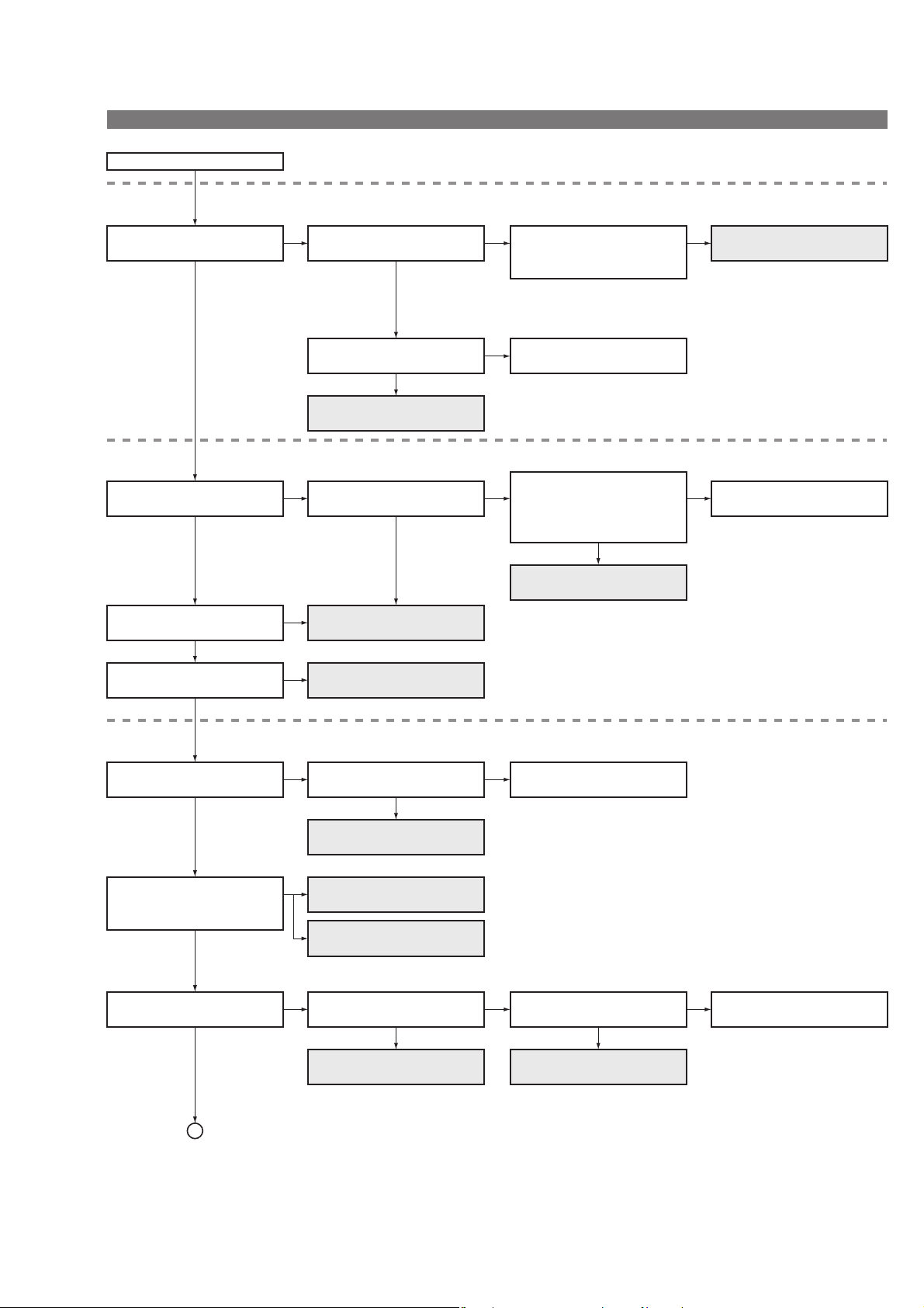
3.1.1 FLOWCHART OF FAILURE ANALYSIS FOR THE WHOLE UNIT
Flowchart of Failure Analysis for The Whole Unit
START
Problems concerning STB status
Is the STB LED lit?
Yes Yes
Problems concerning the power
Can the unit be turned on
(Relay ON)?
Yes
A shutdown occurs.
No
A power-down occurs.
No
Problems concerning lighting of the panel
No
Is STB 3.3 V power supplied?
Is the voltage at AC_DET on the
POWER SUPPLY Unit high?
Yes
Failure analysis for the
MAIN Assy. ⇒ ST1
No
Is the power shutdown?
Yes
Yes
See "Shutdown diagnosis." ⇒ SD
Yes
See "Power-down diagnosis." ⇒ PD
No
Check if the CN304 "P12" cable
that connects the POWER SUPPLY
and DD Assys is firmly connected.
No
Replace the POWER SUPPLY
Unit.
Is the voltage at the RELAY port
No
of the connectors between the
DIGITAL and POWER SUPPLY
Assys H (3.3 V)?
Yes
Failure analysis for the
POWER SUPPLY Unit. ⇒ PS2
A power-down will not be generated if the drive is off.
NG
No
Failure analysis for the
POWER SUPPLY Unit. ⇒ PS1
Replace the MAIN Assy.
Does the screen display reset
lighting?
Yes
Is the panel arbitrary turned on or
off repeatedly? Or do luminescent
spots appear on the screen?
No
Is there any local abnormality
on the screen?
No
A
No
Is the drive off?
Failure analysis for the
drive system ⇒ DR1
Yes
Failure analysis for the
POWER SUPPLY Unit. ⇒ PS3
Failure analysis for the
drive system ⇒ DR2
Yes
Yes
Is the abnormality associated
with one address or one TCP?
Failure analysis for the
drive system ⇒ DR3
No
Yes
Yes
Turn the drive on.
In a case where luminescent spots appear
or the panel is repeatedly turned on or off
In a case where luminescent spots appear
No
Is the abnormality associated
with a single scan line?
Yes
Failure analysis for the
drive system ⇒ DR4
• Check the DRF SW.
• Before turning the drive off with the RS-232C
commands or using the remote control unit,
turn the unit off.
No
Replace the panel chassis.
27
Page 20
A
In the subsequent diagnostic steps, it is most likely that the multi base section is in failure.
Problems concerning video display
Is the panel mask properly
displayed?
Yes
Check with the animated slanting ramp mask. [MKC S03]
Is the on-screen display (OSD)
properly displayed?
Yes
Check on the Factory menu.
Is an external video signal
displayed properly?
Yes
Problems concerning the audio output
Is the audio signal output?
Yes
Do receive a key signal of
a remote control unit?
Yes
No
Failure analysis for the
drive system ⇒ DR2
No
Failure analysis for the
DIGITAL Assy ⇒ DG1
No
Failure analysis for the
MAIN Assy ⇒ MA1
No
Failure analysis for the
audio system ⇒ AU1
No
Failure analysis for the
remote receiver unit ⇒ RM
Specific failure whose cause is
difficult to identify in the initial stage
28
Page 21
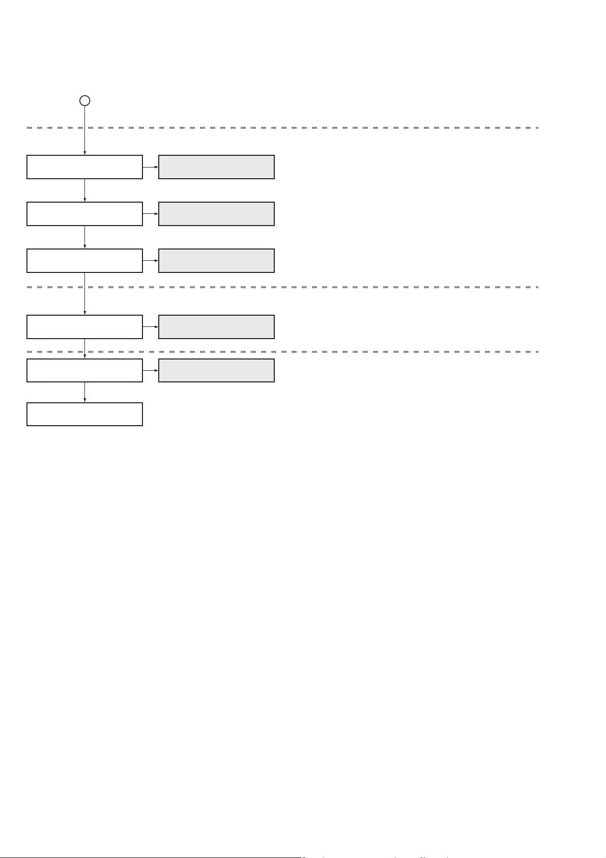
3.1.2 FLOWCHART OF FAILURE ANALYSIS FOR STANDBY STATUS
(1) No power
Note: When an abnormality is detected and indicated by LEDs' flashing or
lighting, all power-supply lines, except for the 7-V DC (M+7 V) and 5-V
ST1
Is 6.8 V DC output from Pin 1
of the CN9006 "PM" connector?
Is 6.8 V DC output from Pin 1
of the CN9009 "PW" connector?
DC (M+5 V) lines, will be automatically shut off after about 10 seconds.
When you are going to check the power-supply lines other than the 7-V
DC (M+7 V) and 5-V DC (M+5 V) lines, place a tester to a measurement
point beforehand then check the line.
NO
Turn the main power on with the cable to
the CN2602 "LD" connector disconnected.
YES
Check if 6.8 V DC is output.
Failure in the CN2602 "LD" connector or
YES
LED Assy (failure in the M5V line at
NO
Pin 5 of the CN2602 "LD" connector)
Failure in the CN9009 "PW" connector or
PWR Assy (failure in S2601 when 6.8 V DC is
applied to the terminal connected to Pin 5 of
the CN9009 "PW" connector but when 6.8 V
DC is not output from the terminal connected
to Pin 1 of the CN9009 "PW" connector)
Is 6.8 V DC output from Pin 6
of the CN9006 "PM" connector?
Failure in the CN9006 "PM" connector or
MAIN Assy (failure in the printed wiring of
board patterns between Pin 1 of the CN9009
"PW" connector and Pin 6 of the CN9006
"PM" connector).
Is 5 V DC output from Pin 4
of the CN9009 "PW" connector?
NO
NO
YES
YES
YES
NO
Disconnect the CN9009 "PW" connector.
Check if 6.8 V DC is output.
Failure in the CN9009 "PW" connector or
PWR Assy (failure in the M5V line at
Pin 5 of the CN2602 "LD" connector,the
SW7 line at Pin 1 of the CN9009 "PW"
YES
connector, the POIN line at Pin 2 of the
CN9009 "PW" connector, the 5-V line at
Pin 4 of the CN9009 "PW" connector or
the M7V line at Pin 5 of the CN9009
NO
Failure in the DD Assy.
(See section T61.)
"PW" connector)
B
Failure in the LED Assy (failure in D2101 or the
CN2602 "LD" connector) or in the MAIN Assy
(failure in the line for the CN9009 "PW"
connector or CN2602 "LD" connector)
29
Page 22
B
Turn the main power on with the cable to
the CN2602 "LD" connector disconnected.
Check if 5 V DC is output.
YES
NO
Turn the main power on with the cable to
the CN9010 "RS" connector disconnected.
Check if 5 V DC is output.
YES
NO
Is 5 V DC output from Pin 5
of IC9502?
YES
Is 3.3 V DC output from Pin 4
of IC9503?
NO (1)
NO (2)
YES
NO
Failure in the CN2602 "LD" connector or LED Assy
(failure in the M5V line at Pin 5 of the CN2602 "LD"
connector)
Failure in the CN9010 "RS" connector or 232C Assy
(failure in the M5V line at Pin 1 of the RS connector)
NO
Is 6.8 V DC input to Pin 1 of IC9502.
YES
Failure in the MAIN Assy.
(failure in IC9502)
Is 6.8 V DC input to Pin 2 of IC9503.
YES
Failure in the MAIN Assy.
(failure in IC9503)
Failure in the MAIN Assy.
(failure in the printed wiring
of board patterns between
Pin 1 of CN9006 "PM" and
pin 1 of IC9502)
NO
Failure in the MAIN Assy.
(failure in the printed wiring
of board patterns between
Pin 2 of IC9503)
Is 0 V DC output from Pin 14
of CN8502 "AD2"?
YES
Failure in the MAIN ASSY (failure in IC9501 or X9501)
Note: If IC9501 is in failure, replace the whole board.
Failure in MAIN Assy
CN2601 "PW" or CN2002 "RS" conector area
NO (4.7V)
Failure in the CN8502 "AD2" connector or MAIN
Assy (failure in IC9501 or X9501)
Note: If IC9501 is in failure, replace the MAIN Assy.
Note :
To check the power supply to the MAIN Assy and AUDIO Assy, follow the procedures described in "DD ASSY
Troubleshooting Chart" (T60 to T64).
For details on statuses of the unit and voltages of each block, see "7.2 CONNECTION PIN EXPLANATION."
30
Page 23
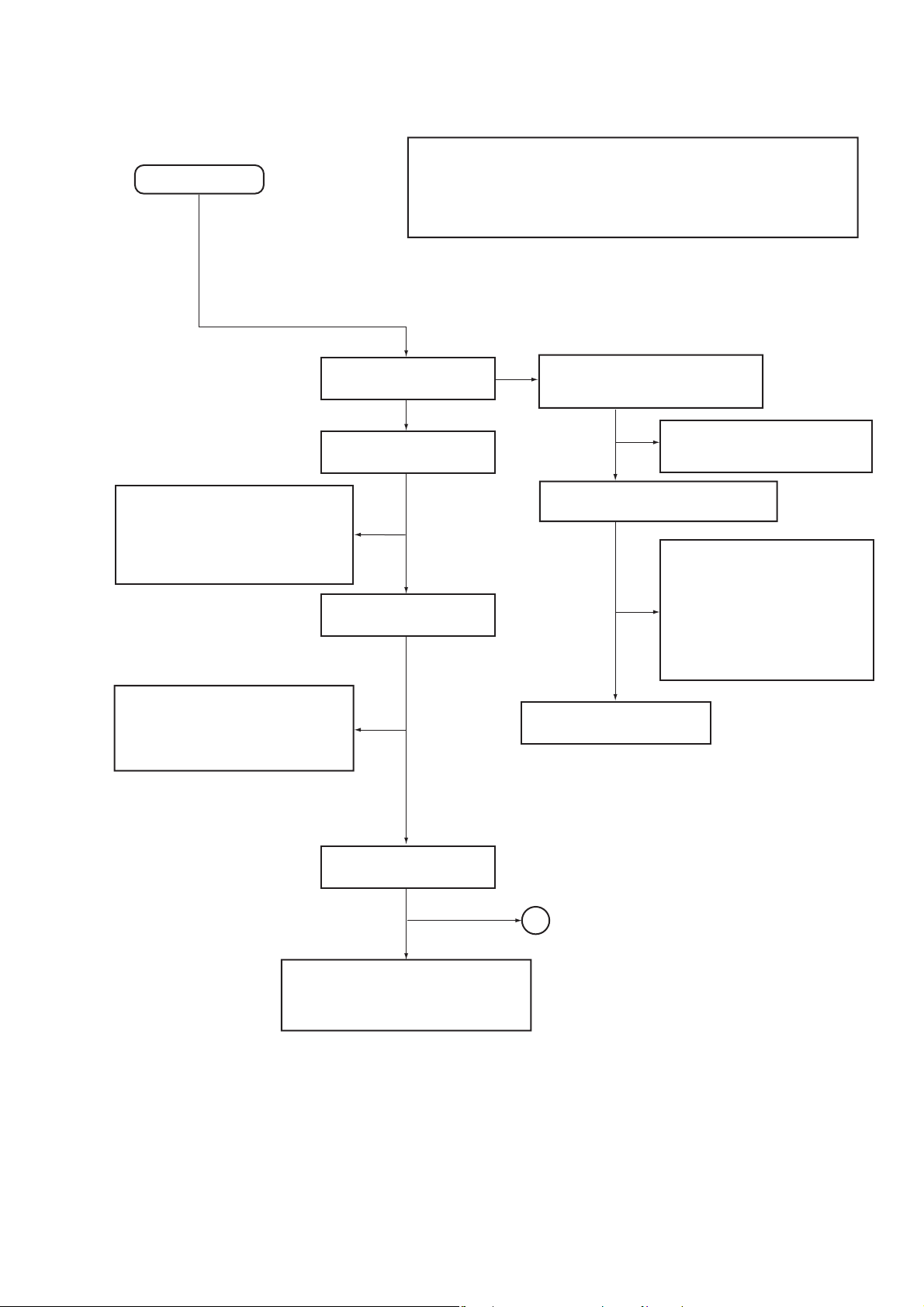
3.1.3 FLOWCHART OF FAILURE ANALYSIS FOR THE POWER SUPPLY UNIT
Flowchart of Failure Analysis for The POWER SUPPLY Unit
Failure analysis for the
POWER SUPPLY Unit. ⇒ PS1
STB 3.3 V power is not output.
Is the cable connected firmly to
the P4 connector?
Yes
Is the cable to the P4 connector
broken?
No
Is the cable connected firmly to
the P12 connector?
Yes
Is the cable to the P12 connector
broken?
No
Is the fuse (F101, F102) blown?
No
Is one of the limiting resistors
(R101/R102) blown?
No
The POWER SUPPLY Unit is
normal.
No
Properly connect the cable between the P4 and
CN3601 "D21" of DIGITAL Assy connectors.
Yes
Replace the defective cable .
No
Properly connect the cable between the P12 and
CN304 "P12" of DD Assy connectors.
Yes
Replace the defective cable.
Yes
Replace the POWER SUPPLY
Unit.
Yes
Replace the POWER SUPPLY
Unit.
Check the voltage at the DIGITAL Assy and
POWER SUPPLY Unit.
Check the voltage at the DD Assy and
POWER SUPPLY Unit.
Check the resistance between F101
and the JW199, using a tester.
Failure analysis for the
POWER SUPPLY Unit. ⇒ PS2
Failure analysis for the
POWER SUPPLY Unit. ⇒ PS3
The power is not on, even though
the RELAY port is active.
Is the relay (RY102) on?
Yes
Is the PFC voltage normal?
Yes
The POWER SUPPLY Unit is
normal.
The cells of the panel do not
light normally.
Is the VADR voltage within the
specified values?
Yes
Is there a fluctuation in the
VADR voltage?
No
Is the VSUS voltage within the
specified range?
Yes
Is there a fluctuation in the
VSUS voltage?
No
The POWER SUPPLY Unit is
normal.
No
Replace the POWER SUPPLY
Unit.
No
Replace the POWER SUPPLY
Unit.
No
Replace the POWER SUPPLY
Unit.
Yes
Replace the POWER SUPPLY
Unit.
No
Replace the POWER SUPPLY
Unit.
Yes
Replace the POWER SUPPLY
Unit.
• Check the relay operation at the terminal
(Pin 11 of P4). (Voltage: 3.3 V)
• Check the relay sound (click).
• Check the voltage between the JW140 (PFC
OUT) and JW180 (Hot_GND) terminal.
• The voltage must be around 390 V
(failure if it is 340 V or less).
Caution: High voltage!
The specified voltage values are between
57 and 63 V.
The ripple must be within 6 V.
The specified voltage values are between
200 and 210 V (VSU: 125/35°C).
The ripple must be within 10 V.
31
Page 24
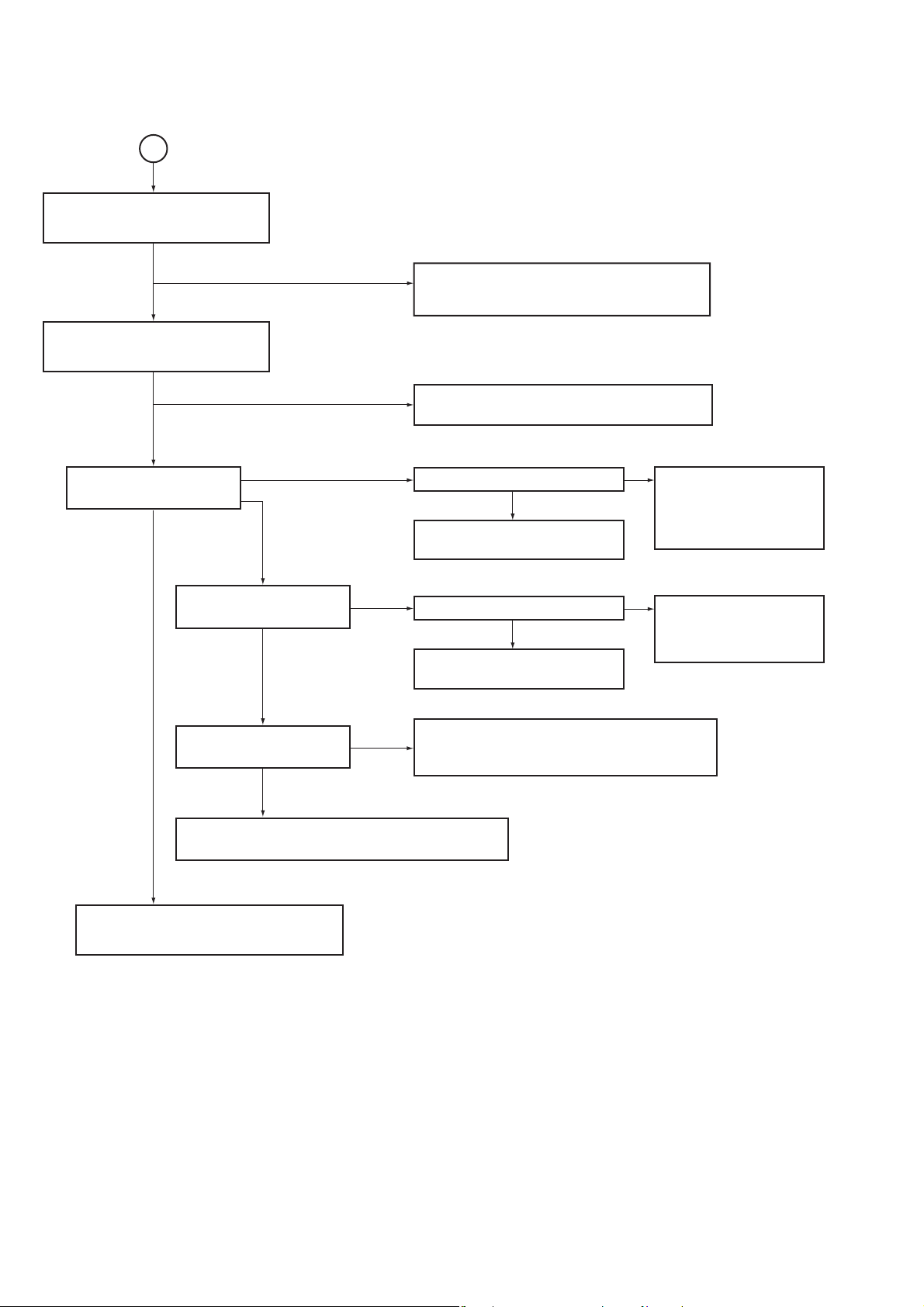
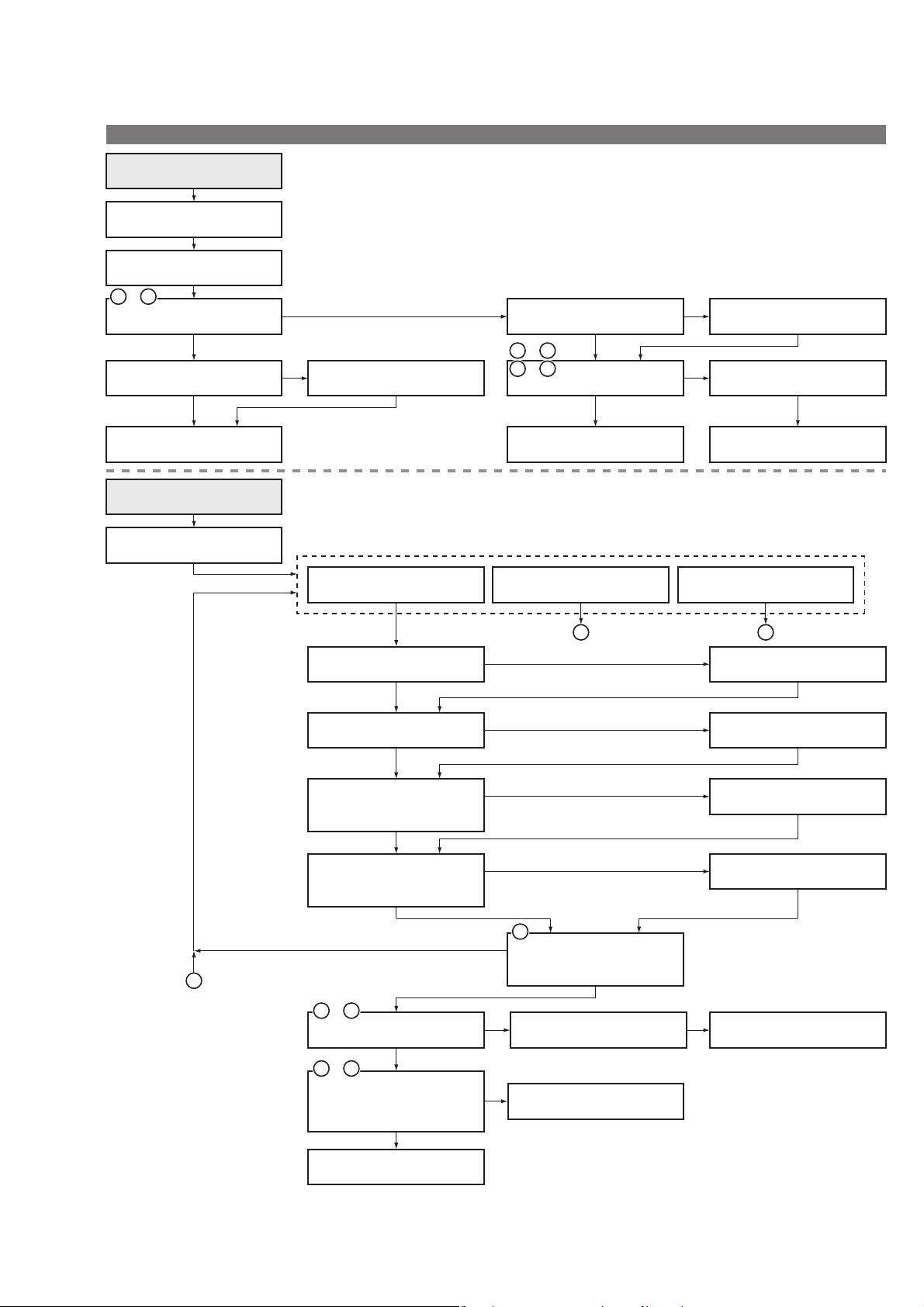
3.1.4 FLOWCHART OF FAILURE ANALYSIS FOR THE DD ASSY
DD ASSY (ANP2173) Trouble Shooting Chart
(1) Trouble Shooting of the "S+12V" output abnormal operation.
Check of S+12V power supply line
Is the S+12V output of CN309
"PA" (#1-3) normally 12.0 V?
Please check the voltage.
YES
NO
NO
NO
Please check the loose contact about
CN309 "PA" connector wire.
Is this contact OK?
YES
After remove the CN309 "PA" connector
wire, please check the S+12V output
line is shorten or not by using the D.M.M.
Is this line shorten?
YES
Please check the C334 and C335
electrolytic capacitors shorten.
Are these capacitors OK?
YES
Is normal voltage output after CN309
"PA" is disconnected?
NO
NO
YES
T60
Please replace the
connector wire.
Please replace these
capacitors.
See "Abnormal in Audio
Trouble shooting".
Is the VCC16.5V input of CN301 "P5" (#1)
normally between 15.7 V and 17.3 V?
Please check this voltage.
Check the S+12V output (CN309 #1 - #3 "PA").
NO
Please check the loose contact about
CN301 "P5" connector wire.
Is this contact OK?
NO
YESYES
Please check the waveform of IC305
#11 - #14 (MD3222N) control IC.
Can you see the same waveform?
Please check the FU302 protector
opened.
Is this protector opened?
NO
YES
YES
In this case, the S+12V P.S. is normally operating.
Please check the AUDIO Assy, speaker units,
speaker cord and audio signal source input.
Please replace the connector wire.
YES
NO
In this case, the S+12V P.S. is normally operating.
Please check the AUDIO Assy, speaker units,
speaker cord and audio signal source input.
In this case, it's possibility of the
AC-DC P.S. unit out of order.
Please replace of the unit.
Please replace IC305 or D306 or
D307.
In this case, any of S+12V power
supply control IC305 or D306 or
D307 or C334 is broken.
Please replace IC305 or C326 or C327 or C328 or
C337.
In this case, S+12V power supply control IC305 or
any of C326, C327, C328, C337 capacitors of the
VCC16.5V input line is broken.
32
• Legend symbol
: This symbol is for directing the broken
T10
parts on "Diagnosis Points of PCB Assy".
Page 25
(2) Trouble Shooting of the "M+7V" output abnormal operation.
Check of M+7V power supply line
Can you hear the power
relay operation sound?
NO
YES
YES
Is the M+7V output of CN305 #1
"PM" normally about 7 V?
Please check the voltage.
NO
YES
NO
YES
Is the STB3.3V input of CN301
"P12" (5-7) normally 3.3 V ?
Please check the voltage.
YES
NO
Please check the loose contact about CN301
"P12" connector wire.
Is this contact OK?
YES
YES
Is this connector wire contact OK?
After remove the CN305 "PM" connector
wire, please check the M+7V output line is
shorten or not by using the D.M.M.
Is this line shorten?
YES
Please check the C302 electrolytic
capacitor and D302 TVS. shorten.
Are these parts OK?
In this case, the M+7V DD Assy part
is normally operating.
Check the MAIN Assy board.
NO
Please replace the connector wire.
NO
NO
T61
Please replace the connector
wire.
Please replace these
capacitor.
Check the Q301 FET (micro PA1725G)
drain terminal (#5 - #8) waveform.
Can you see the same waveform?
Check the Q301 FET (uPA1725G)
gate terminal (#4) waveform.
(3.3 V rectangular pulse)
Can you see the waveform?
Please check the FU301 protector opened.
Is this protector opened?
NO
In this case, it's possibility of the AC-DC
P.S. unit out of order.
Please replace of the unit.
NO
YES
33
YES
NO
YES
In this case, the M+7V DD Assy part
is normally operating.
Check the MAIN Assy board.
In this case, IC301 is broken.
Please replace of this IC.
Please replace Q301 FET, IC301
(LM3478MMX), D301.
In this case, any of IC301 (M+7V
power supply control IC) or Q301 or
D301 is fault.
In this case, Q301 FET is broken.
Please replace Q301 and FU301.
• Legend symbol
: This symbol is for directing the broken
T10
parts on "Diagnosis Points of PCB Assy".
Page 26
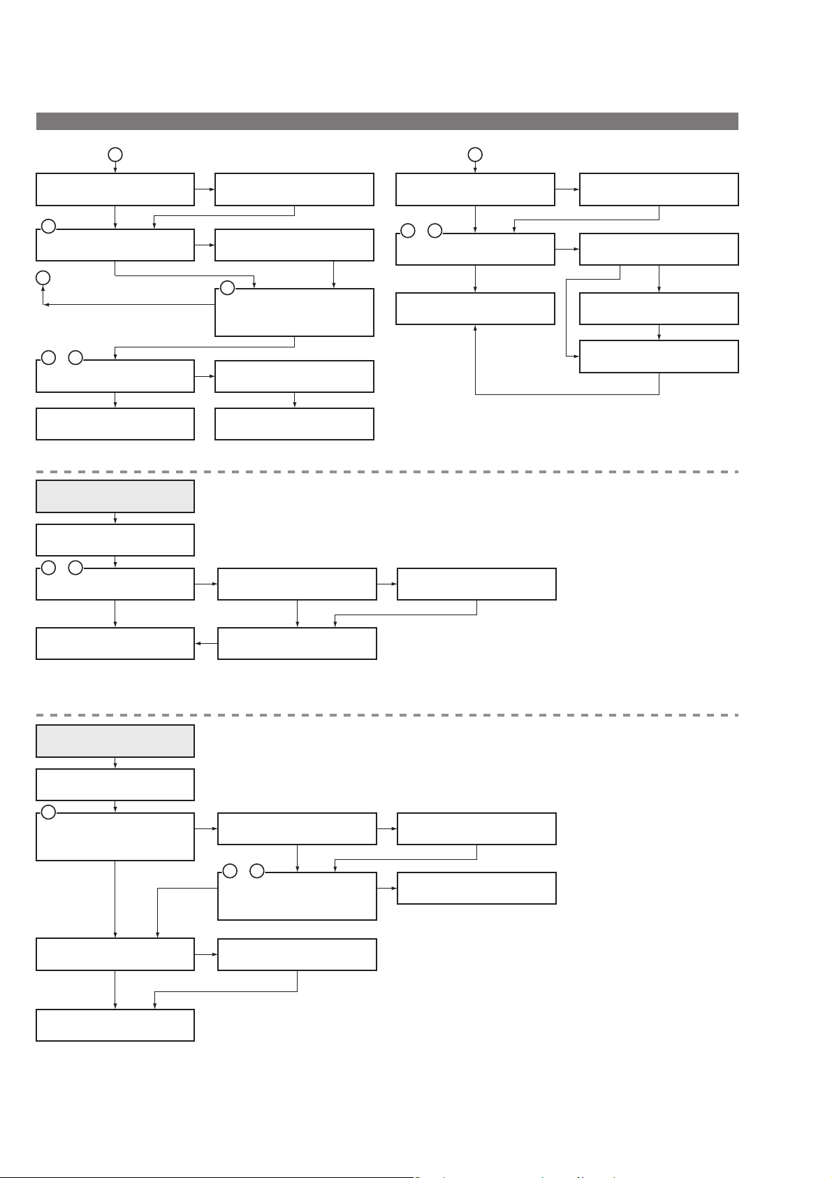
(3) Trouble Shooting of the "D+3.3V" output abnormal operation.
Check of D+3.3 power supply line
In this case, the D+3.3 V output is fallen
down. The low voltage alarm on the
MAIN Assy is functioned.
60 inch models
50 inch models
Is the D+3.3V output of CN307 "PN"
(#1-#3) normally 3.3 V?
Please check the voltage.
NO
Is the D+3.3 V output of CN307 "PN"
(#1-#3) normaly 3.3 V?
Please check the voltage.
NO
Is the VCC+3.3V input of CN302
"P8" (#7-#10) normaly 3.3 V?
NO
Failure in the POWER SUPPLY Unit or
loose contact of CN302 "P8" connector
Please check the loose contact
about CN307 "PN", connector wire.
Is this contact OK?
YES
After remove the PN connector wire,
please check the D+3.3V output line
is shorten or not by using the D.M.M.
Is this line shorten?
T62
YES
Failure in the MAIN Assy
YES
Failure in the DD Assy
NO
Please replace the connector
wire.
Please replace C320.
YES
In this case, C320 electrolytic
capacitor is shorten.
YES
Is the VCC5.1V input of CN302 "P8"
(#7-#10) normally between 4.85 V and
5.36 V?
Please check this voltage.
NO
YES
Check the waveform of Q303 FET
drain terminal (#5-#8).
Can you see the same waveform?
NO
Check the Q302 FET (TPC8021-H)
gate terminal (#4) waveform.
(About 8 -10V0-p rectangular pulse)
Can you see the same waveform?
• Legend symbol
: This symbol is for directing the broken
T10
parts on "Diagnosis Points of PCB Assy".
NO
Please check the loose contact about
CN302 "P8" connector wire.
Is this contact OK?
YES
In this case, the MAIN ASSY side is
YES
NO
YES
34
abnormal.
See the LED indicators about trouble
shooting chart or trouble shooting chart
of "Abnormally in image".
In this case, any of the IC303 or FET
Q302 or D304 (bootstrap diode) is
broken.
Please replace IC303 or FET Q302 or
D304.
In this case, any of the IC303 or FET
Q302 or D304 (bootstrap diode) is
broken.
NO
In this case, it's possibility of the
AC-DC P.S. unit out of order.
Please replace of the unit.
Please replace the
connector wire.
Page 27
(4) Trouble Shooting of the "A+12V" output abnormal operation.
This voltage Line is supplied for analog circuit and the fan motors VCC voltage through the variable voltage regulator
on the MAIN ASSY.
The output voltage of the variable voltage regulator is DC 11.6 V or DC 8.8 V or DC 6.0 V.
And, no operation fan motors by acting fan alarm signal is not mentioned on this item.
Check of A+12V power supply line
At first, please check the A+12V output
CN306 "PV" (#1).
Please check the voltage is about
12.2 V.
YES
Is the VCC16.5V input of CN301 "P5"
(#1) normally between 15.7 V and
17.3 V?
Please check this voltage.
YES
NO
Please check the waveform of
IC302 (A+12V control IC;
MPS2367DN) #3 pin.
Can you see the same waveform?
Please check the loose contact
NO
about CN306 "PV", connector wire.
Is this contact OK?
YES
After remove the PV connector wire,
please check the A+12V output line is
shorten or not by using the D.M.M.
Is this line shorten?
YES
Please check the loose contact about
CN301 "P5" connector wire.
Is this contact OK?
NO
T63
NO
Please replace the connector
wire.
Please replace C311, C312
NO
capacitors and D303
(flywheel Diode) shorten.
Please replace the
NO
connector wire.
In this case, it's possibility
YES
of the AC-DC MAIN
POWER unit out of order.
Please replace of the unit.
Please replace IC302 or D312.
In this case, any of IC302
(A+12V control IC; MPS2367DN)
or D312 is broken.
(5) Trouble Shooting of the "A+6.5V" output abnormal operation.
This voltage Line is supplied to MAIN ASSY from MAIN POWER unit via DD ASSY.
Please check board to board connection first if A+6.5V is abnormal.
e.g.) pin contact of connector, short between wire
From MAIN POWER unit
P12 CN304 (#1)
From MAIN POWER unit
P8 CN302 (#1)
To MAIN ASSY
"PV" CN306 (#3, #4)
DD ASSY
35
YES
In this case,the A+12V output of
the MAIN ASSY side is abnormal.
T64
• Legend symbol
: This symbol is for directing the broken
T10
parts on "Diagnosis Points of PCB Assy".
Page 28
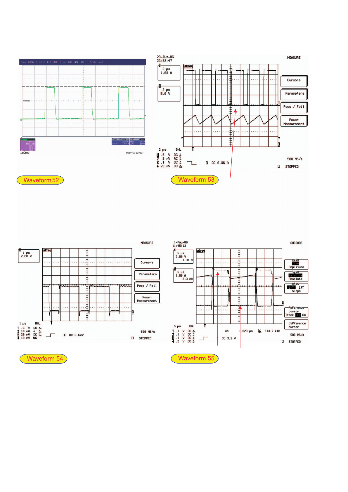
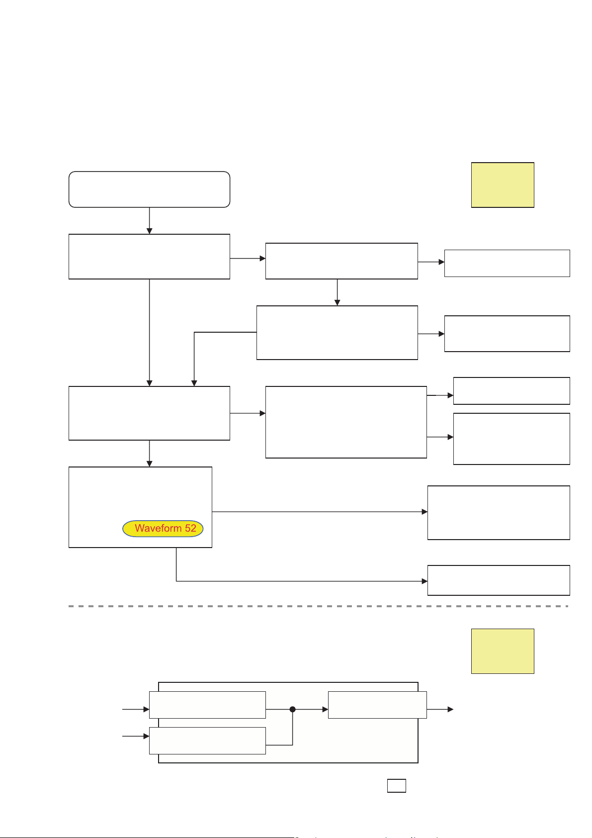
DD ASSY (ANP2173) Waveform (Each 4 Switching Regulators)
A+12V POWER SUPPLY
IC302 #3 voltage waveform.
5 V/div., 1 μs/div.
Normal: 18.2 V0-p, T= 2.95 μs
S+12V POWER SUPPLY
Upper side waveform
IC305 #11-#14 voltage waveform.
5 V/div., 2 μs/div.
Normal: 17.5V0-p, T= 3.3 μs
D+3.3V POWER SUPPLY
Q303 FET Drain terminal (#5-#8)
voltage waveform.
2 V/div., 1 μs/div.
Normal: 6.0 V0-p, T= 3.3 μs
M+7V POWER SUPPLY
Q301 FET Drain terminal (#5-#8)
voltage waveform.
2 V/div., 0.5 μs/div.
Normal: 8.0 V0-p, T= 2.6 μs
36
Page 29
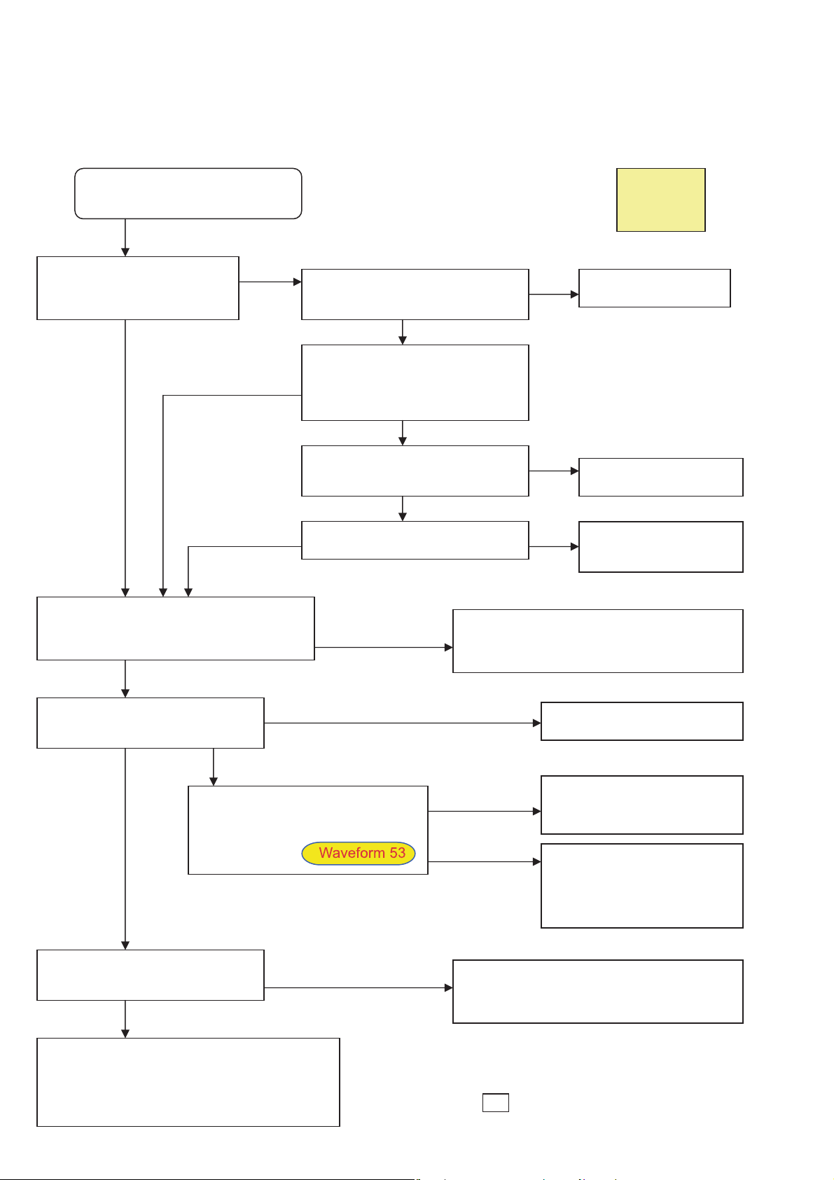
3.1.5 FLOWCHART OF FAILURE ANALYSIS FOR THE DRIVE ASSY
Flowchart of Failure Analysis for The Drive Assy (1)
Failure analysis for the
drive system ⇒ DR1
Reset lighting is not displayed.
X/Y DRIVE Assys
7 9
to
Is the waveform normal when the
voltage is applied to the panel?
Are the panel FFC cables properly
connected to the X/Y DRIVE Assys?
Yes
No
No
Properly connect the panel
FFC cables.
NG
Are the FFC cables properly
connected?
17 24
to
31 35
to
Is the input signal normal?
Yes
Yes
No
Properly connect the FFC cables.
NGYes
No
Replace the FFC cables.
NG
Replace the panel chassis.
Failure analysis for the
drive system ⇒ DR2
Abnormality across the whole
screen, such as luminescent spots
Yes
Another Assy may be in failure.
E
Replace the X/Y DRIVE Assys.
Because it is difficult to identify which drive is in failure, follow the flowchart below to check each Assy.
X DRIVE AssyY DRIVE Assy / SCAN Assy
C
Are all the connectors properly
connected?
Yes
Is the VH set voltage (130 V)
correctly set?
Yes
Is the VOFS set voltage
correctly set (set value: designated
for each panel)?
Yes
Is the VYPRST set voltage correctly
set (set value: designated for
each panel)?
Yes
12 16
to
Is the input signal normal?
(See the oscilloscope photos.)
17 24
to
Is the waveform of the control
signal from the SCAN Assy
normal?
(See the oscilloscope photos.)
Yes
Yes
No
No
No
No
9
Yes
Is the waveform normal when the
voltage is applied to the panel?
(See the oscilloscope photos.)
No
No
Replace the FFC cables. Replace the DIGITAL Assy.
No
Replace the Y DRIVE Assy.
Replace the DIGITAL Assy.
ADDRESS Assy
D
Reconnect the connectors.
Replace the Y DRIVE Assy.
Set the VOFS voltage correctly.
Set the VYPRST voltage correctly.
NG
NG
NG
NG
NG
Replace the SCAN Assy.
37
Page 30
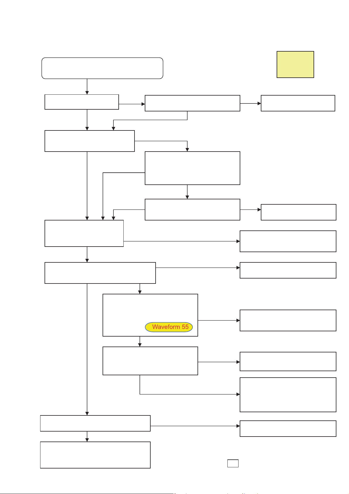
Flowchart of Failure Analysis for The Drive Assy (2)
X DRIVE Assy
C
Are all the connectors properly
connected?
Yes
36
Is the VXNRST set voltage
(-180 V) correctly set?
Yes
E
Another Assy may be in failure.
10 11
to
Is the input signal normal?
(See the oscilloscope photos.)
Yes
Replace the X DRIVE Assy.
Failure analysis for the
drive system ⇒ DR3
The abnormality is associated with
one address or one TCP?
2 6
to
Is the TCP control signal normal?
Yes Yes
Replace the panel chassis.
In most cases of damage on one line,
the panel chassis must be replaced.
No
Reconnect the connectors.
NG
No
Replace the X DRIVE Assy.
7
Yes
Is the waveform normal when the
voltage is applied to the panel?
(See the oscilloscope photos.)
No
No
Replace the FFC cables.
NG
Replace the DIGITAL Assy.
Diagnose the ADDRESS Assy.
No
Are the FFC cables properly
connected?
NG
Replace the DIGITAL Assy.
NG
ADDRESS Assy
D
Are all the connectors properly
connected?
Yes
2 6
to
Is the TCP control signal normal?
(See the oscilloscope photos.)
Yes
Replace the panel chassis.
No
Properly connect the FFC cables.
NG
If the FFC cable that connects the DIGITAL and ADDRESS Assys is in failure,
the abnormality is associated with one address in most cases.
No
Reconnect the connectors.
No
Are the FFC cables properly
connected?
Yes No
Properly connect the FFC cables.
Replace the DIGITAL Assy.
NG
NG
NG
Failure analysis for the
drive system ⇒ DR4
The abnormality is associated
with a single scan line.
9
Is the waveform normal when the
voltage is applied to the panel?
(See the oscilloscope photos.)
Yes
Is the cable connected properly
to the 90-pin connector?
Yes
Replace the SCAN Assy.
Diagnose the SCAN Assy.
No
Is the cable connected properly
to the 15-pin connector?
Yes
17 24
to
Yes
Is the waveform of the SCAN IC
control signal from the Y DRIVE
Assy normal?
No
Connect the cable properly.
NG
No
Connect the cable properly.
NG
No
Replace the Y DRIVE Assy.
Care must be taken that no dirt or dust is attached or gets in.
(The SCAN IC may be damaged.)
38
Page 31

60 ADDRESS ASSY
• ADR LOGIC BLOCK
1) input: VIDEO 60Hz
signal: COLOR BAR (MKSS17)
ch1: L1730 (V+ADR1) (side-A through hole)
1
V: 10 V/div H: 2 mS/div
ch2: IC1601 or IC1801 28 pin (R_E) side-A test plane "R_E"
2
V: 1 V/div H: 2 mS/div
ch3: IC1601 or IC1801 38 pin (CLK) side-A test plane "CLK1"
3
V: 1 V/div H: 2 mS/div
ch4: IC1601 or IC1801 (LE_E) side-A test plane "LE_E"
4
V: 1 V/div H: 2 mS/div
ch5: IC1601 or IC1801 45 pin (HBLK) side-A test plane "HBLK"
5
V: 1 V/div H: 2 mS/div
ch6: IC1601 or IC1801 44 pin (LBLK) side-A test plane "LBLK"
6
V: 1 V/div H: 2 mS/div
2) input: VIDEO 60Hz
signal: Checkered pattern of Black- White (MKSS13)
CH1: L1730 (V+ADR1) (side-A through hole)
1
V: 10 V/div H: 2 mS/div
CH2: IC1601 or IC1801 28 pin (R_E) side-A test plane "R_E"
2
V: 1 V/div H: 2 mS/div
CH3: IC1601 or IC1801 38 pin (CLK) side-A test plane "CLK1"
3
V: 1 V/div H: 2 mS/div
CH4: IC1601 or IC1801 (LE_E) side-A test plane "LE_E"
4
V: 1 V/div H: 2 mS/div
CH5: IC1601 or IC1801 45 pin (HBLK) side-A test plane "HBLK"
5
V: 1 V/div H: 2 mS/div
CH6: IC1601 or IC1801 44 pin (LBLK) side-A test plane "LBLK"
6
V: 1 V/div H: 2 mS/div
ch1
ch2
ch3
ch4
ch5
ch6
• Incoming signals of TCP (1Field)
3) input : VIDEO
signal:Checkered pattern of Black- White (MKSS13)
CH1: L1730 (V+ADR1) (side-A through hole)
1
V: 10 V/div H: 500 nS/div
CH2: IC1601 or IC1801 28 pin (R_E) side-A test plane "R_E"
2
V: 1 V/div H: 500 nS/div
CH3: IC1601 or IC1801 38 pin (CLK) side-A test plane "CLK1"
3
V: 1 V/div H: 500 nS/div
CH4: IC1601 or IC1801 (LE_E) side-A test plane "LE_E"
4
V: 1 V/div H: 500 nS/div
CH5: IC1601 or IC1801 45 pin (HBLK) side-A test plane "HBLK"
5
V: 1 V/div H: 500 nS/div
CH6: IC1601 or IC1801 44 pin (LBLK) side-A test plane "LBLK"
6
V: 1 V/div H: 500 nS/div
ch1
ch2
ch3
ch4
ch5
ch6
ch1
ch2
ch3
ch4
ch5
ch6
• Incoming signals of TCP (1Field)
• Incoming signals of TCP (Resonance part)
39
Page 32

60 X DRIVE ASSY, 60 Y DRIVE ASSY, 607 SCAN A ASSY, 607 SCAN B ASSY
ch3: R1222 (XPSUS) - K1201(SUSGND)
7
V: 100 V/div H: 2 mS/div
(60 X DRIVE Assy)
ch4: K2801 to K2812, K2901 to K2912
8
(Scan OUT) - K2301 (SUSGND)
V: 100 V/div H: 2 mS/div
(607 SCAN B Assy HIGH SIDE)
ch5: R2288 (YPSUS) - KN2203 (SUSGND)
9
V: 100 V/div H: 2 mS/div
(60 Y DRIVE Assy)
ch3: K1012 (XSUS-MSK) - K1002 (DGND)
10
V: 1 V/div H: 2 mS/div
(60 X DRIVE Assy)
ch4: K1008 (XNR-D) - K1002 (DGND)
11
V: 1 V/div H: 2 mS/div
(60 X DRIVE Assy)
ch3
ch1: K2007 (YNOFS) - K2014(DGND)
12
V: 1 V/div H: 2 mS/div
(60 Y DRIVE Assy)
ch2: K2005 (YSUS-MSK) - K2014 (DGND)
13
V: 1 V/div H: 2 mS/div
(60 Y DRIVE Assy)
ch3: K2004 (YNRST) - K2014 (DGND)
14
V: 1 V/div H: 2mS/div
(60 Y DRIVE Assy)
ch4: K2003 (SOFT-D) - K2014 (DGND)
15
V: 1 V/div H: 2 mS/div
(60 Y DRIVE Assy)
ch5: K2010 (YPR-U) - K2014 (DGND)
16
V: 1 V/div H: 2 mS/div
(60 Y DRIVE Assy)
ch1: R2401 (LE) - K2014 (DGND)
17
V: 1 V/div H: 2 mS/div
(60 Y DRIVE Assy)
ch2: R2404 (CLK2) - K2014 (DGND)
18
V: 1 V/div H: 2 mS/div
(60 Y DRIVE Assy)
ch3: R2406 (SI_L) - K2014 (DGND)
19
V: 1 V/div H: 2 mS/div
(60 Y DRIVE Assy)
ch4: R2409 (CLR) - K2014 (DGND)
20
V: 1 V/div H: 2 mS/div
(60 Y DRIVE Assy)
ch5: R2411 (OC2_U) - K2014 (DGND)
21
V: 1 V/div H: 2 mS/div
(60 Y DRIVE Assy)
ch6: R2415 (OC1) - K2014 (DGND)
22
V: 1 V/div H: 2 mS/div
(60 Y DRIVE Assy)
ch7: R2418 (CLK1) - K2014 (DGND)
23
H: 2 mS/div
(60 Y DRIVE Assy)
ch8: R2420 (SI_H) - K2014 (DGND)
24
H: 2 mS/div
(60 Y DRIVE Assy)
ch3
ch4
ch5
ch1: R1222 (XPSUS) - K1201 (SUSGND)
25
V: 100 V/div H: 100 μS/div
(60 X DRIVE Assy)
ch2: K2801 to K2812, K2901 to K2912
26
(ScanOUT) - K2301 (SUSGND)
V: 100 V/div H : 100 μS/div
(607 SCAN B Assy HIGH SIDE)
ch3: F2301 (YPSUS) - KN2206 (SUSGND)
27
V: 100 V/div H: 100 μS/div
(60 Y DRIVE Assy)
ch1: R1222 (XPSUS) - K1202 (SUSGND)
28
V: 50 V/div H: 5 μS/div
(60 X DRIVE Assy)
ch2: K2801 to K2812, K2901 to K2912
29
(ScanOUT) - K2301 (SUSGND)
V: 50 V/div H: 5 μS/div
(607 SCAN A Assy LOW SIDE)
ch3: F2301 (YPSUS) - K2301 (SUSGND)
30
V: 50 V/div H: 5 μS/div
(60 Y DRIVE Assy)
ch4
ch1
ch2
ch4
ch3
ch1: F2301 (YPSUS) - K2301 (SUSGND)
31
V: 50 V/div H: 500 nS/div
(60 Y DRIVE Assy)
ch2: K2002 (YSUS-G) - K2014 (DGND)
32
V: 5 V/div H : 500 nS/div
(60 Y DRIVE Assy)
ch3: K2013 (YSUS-U) - K2014 (DGND)
33
V: 5 V/div H: 500 nS/div
(60 Y DRIVE Assy)
ch4: K2011 (YSUS-B) - K2014 (DGND)
34
V: 5 V/div H: 500 nS/div
(60 Y DRIVE Assy)
ch5: K2012 (YSUS-D) - K2014 (DGND)
35
V: 5 V/div H: 500 nS/div
(60 Y DRIVE Assy)
ch1
ch2
ch3
ch4
ch5
ch1
ch2
ch3
ch4
ch5
ch1
ch2
ch3
ch4
ch5
ch6
ch7
ch8
ch1
ch2
ch3
40
Page 33

IC1801
to
2 6
(ANP2160-A)
(ANP2160-A)
60 ADDRESS S ASSY
IC1601
to
2 6
SIDE A SIDE A
60 ADDRESS L ASSY
41
Page 34

K2911
K2910
K2909
K2908
26 29
8
26 29
8
26 29
8
26 29
8
(ANP2161-A)
K2912
26 29
8
K2907
K2811
K2810
K2809
K2808
(ANP2161-A)
26 29
8
26 29
8
26 29
8
26 29
8
26 29
8
K2807
26 29
8
K2812
K2905
K2904
K2903
26 29
8
K2806
26 29
K2906
26 29
8
K2805
26 29
8
26 29
8
26 29
8
26 29
8
K2804
K2803
K2802
26 29
8
26 29
8
26 29
8
8
SIDE A SIDE A
K2902
26 29
8
607 SCAN B ASSY
K2901
26 29
8
42
607 SCAN A ASSY
K2801
26 29
8
Page 35

SIDE ASIDE A
(ANP2140-A)
R1222
25 28
7
36
R1222
25 28
7
60 X DRIVE
ASSY
43
Page 36

(ANP2166-A)
R2401
R2406
R2411
R2418
17
19
18
20
R2404
R2409
21
22
23
24
R2415
R2420
KN2203
9
K2012
35
K2006
R2288
9
12
K2013
33
K2014
to
to
12 24
31 35
K2011
K2005
13
K2004
14
15
K2003
16
K2010
34
K2301
29 3026
8
60 Y DRIVE ASSY
SIDE A SIDE A
F2301
3027
KN2206
27
44
Page 37

3.1.6 FLOWCHART OF FAILURE ANALYSIS FOR THE DIGITAL ASSY
Flowchart of Failure Analysis for The DIGITAL Assy
Failure analysis for the
DIGITAL Assy ⇒ DG1
The on-screen display (OSD) is
not properly indicated.
Is V sync/H existence judgment
detected by issuing the QSI
command?
Yes
Is the indication position correct?
Yes
• If the OSD is not properly displayed although the panel mask is properly displayed,
a failure exists in the path from the output of IC8201 on the MAIN Assy to IC3401 on the DIGITAL Assy.
→ If only the OSD is abnormal, the MAIN Assy is in failure.
No
Failure analysis for the MAIN Assy
⇒ MA1
No
Is the 50-pin FFC cable firmly
connected? (ADD1472)
Yes
Is the 50-pin FFC cable broken?
(ADD1472)
No
Is the FFC connector poorly
contacted?
No
Failure analysis for the MAIN Assy
⇒ MA1
No
It is most likely that the sync signal is abnormal.
No
Firmly connect the 50-pin FFC
cable.
When disconnecting the FFC cable, take care not to damage the CN3001 connector
on the DIGITAL Assy, which can easily be damaged.
Yes
Replace the 50-pin FFC cable.
In a case of D11
Yes
Replace the DIGITAL Assy.
In a case of AD3
Replace the LVDS Assy.
Is the tone correct?
Yes
Failure analysis for the MAIN Assy
⇒ MA1
No
It is most likely that the video signal data are missing.
45
Page 38

3.1.7 FLOWCHART OF FAILURE ANALYSIS FOR THE MAIN ASSY
Flowchart of Failure Analysis for The MAIN Assy
Failure analysis for the
MAIN Assy ⇒ MA1
Input signal is not displayed.
No
Is the selected input signal a
VIDEO 1 and 2?
No
Is the selected input signal a
DVD/HD1 and 2?
No
Is the selected input signal a
PC?
No
Is the selected input signal a
DVD/HD3 and 4?
Yes
Is the on-screen display (OSD)
properly displayed?
No
Failure analysis for the
LVDS Assy ⇒ LV1
Yes
Failure analysis for
video inputs ⇒ VD
Yes
Failure analysis for
component inputs ⇒ CMP
Yes
Failure analysis for
PC input ⇒ PC
Yes
Failure analysis for
component (HDMI) inputs ⇒ HDMI
Yes
Failure analysis for the
MAIN Assy ⇒ MA3
46
Page 39

Examination of the MAIN ASSY
No image (Examination of the MAIN ASSY)
In a case of inputs to DVD/HD1 and 2 (component inputs)
Failure analysis for
component inputs => CMP
Waveform 1
• Legend symbol
: This symbol is for directing the broken
T10
parts on "Diagnosis Points of PCB Assy".
Are signals input to the input
terminals?
YES
Are signals input to Pins 11, 14,
and 17 (for video) of IC5602?
YES
Are signals input to Pins 8 and
11 (for sync) of IC9504?
NO
Are signals input to Pins 11
and 13 (for sync) of IC5605?
NO
Is a signal input to Pin 3
(for video) of IC5605?
NO
NO
Check the signal output equipment and its cables.
Waveform 2
NO
Failure in the MAIN ASSY
Waveform 3
YES
Failure in the MAIN ASSY
Waveform 5
YES
Failure in the IC9504
Waveform 6
YES
Failure in the IC5605
Failure in the MAIN ASSY
Input Y
Input Pb
Input Pr
IC5602-14 pin
IC5602-11 pin
IC5602-17 pin
Waveform1
Waveform 2
IC9501-17 pin
IC9501-4 pin
IC9504-8 pin
IC9504-11 pin
T10
IC5605-11 pin
IC5605-13 pin
Waveform 3 Waveform 5
IC5605-3 pin
Waveform 4
Waveform 6
47
Page 40

In a case of input to PC
Failure analysis for
PC input => PC
Image Signal : Color bar
Waveforms 7-1, 7-2
• Legend symbol
: This symbol is for directing the broken
T10
parts on "Diagnosis Points of PCB Assy".
Are signals input to the input
terminals?
YES
Are signals input to Pins 4 and
10 (for sync) of IC5006 for the
PC1 input ?
YES
Are signals input to Pins 7 and
9 of IC5902?
YES
Are signals input to Pins 4
and 7 of IC5904?
NO
Check the signal output equipment and its cables.
Waveform 8
NO
IC without a signal output is in failure.
Waveform 9
NO
Waveform 11
NO NO
Are the voltages at Pins 2 and 14 of
IC5902 0 V and 5 V DC, respectively,
for the PC1 input, or 5 V and 0 V DC,
respectively, for the PC2 input?
NO
Are signals input to Pins 2, 30,
and 31 (for control) of IC5301?
YES
Failure in the IC5301
Is the voltage at Pin 1 of
IC5904 0 V DC?
YES
Waveform 10
NO
Failure in the MAIN ASSY
Failure in the MAIN ASSY
Failure in the IC5902
YES
Are signals input to Pins 11
and 13 of IC5903?
YES
Are signals input to Pins 3
and 6 of IC5906?
YES
Are signals input to Pins 3
and 6 of IC9504?
YES
Failure in the MAIN ASSY
Waveform 13
NO
Waveform 14
NO
Waveform 15
NO
Failure in the IC5903
Failure in the IC5906
Failure in the IC9504
YES
Are signals input to Pins 2, 30,
and 31 (for control) of IC5301?
YES
Failure in the IC5301
Waveform 12
NO
Failure in the MAIN ASSY
T11
48
Page 41

Input R
Input G
IC5301-2 pin
IC5906-3 pin
Input B
IC5301-30 pin
IC5906-6 pin
Waveform 7-1 Waveform 10 Waveform 14
Input V
Input H
IC5904-7 pin
IC5904-4 pin
IC9504-6 pin
IC9504-3 pin
Waveform 7-2 Waveform 11 Waveform 15
IC5004-10 pin
IC5301-2 pin
IC5004-4 pin
IC5902-7 pin
IC5902-9 pin
IC5301-30 pin
Waveform 8 Waveform 12
IC5903-11 pin
IC5903-13 pin
Waveform 9 Waveform 13
49
Page 42

In a case of inputs to VIDEO 1 and 2
Failure analysis for
video inputs => VD
Waveform 22
• Legend symbol
: This symbol is for directing the broken
T10
parts on "Diagnosis Points of PCB Assy".
Are signals input to the input
terminals?
YES
Is signal input to Pin 119
(for video) of IC6201?
YES
Are signals output from Pins 73
and 74 (for sync) of IC6201?
YES
Are signals input to Pins 3
and 6 (for sync) of IC6403?
NO
Is the voltage at Pin 1 (for
control) of IC6403 3.3 V DC?
YES
Failure in the IC6403
NO
Waveform 23
NO
Waveform 24
NO
Waveform 25
YES
NO
Check the signal output equipment and its cables.
Failure in the MAIN ASSY
Failure in the MAIN ASSY
Failure in the MAIN ASSY
Failure in the MAIN ASSY
T13
50
Page 43

Input VIDEO2
IC6201-74 pin
IC6201-73 pin
Waveform 22 Waveform 24
IC6201-119 pin
IC6403-3 pin
IC6403-6 pin
Waveform 23 Waveform 25
51
Page 44

In a case of inputs to DVD/HD3 and 4 (HDMI) (in a theater model)
Failure analysis for
component (HDMI) inputs
=> HDMI
YES
Are approx. 500 mVp-p signals
input to Pins 39 and 40 of
IC7001?
YES
Are approx. 500 mVp-p signals
input to Pins 58 and 59 of
IC7001?
YES
Is the voltage at Pin 4 of
IC7004 1.8 V DC?
YES
Are sync signals input to Pins
2 and 3 of IC7001?
And is a CLK signal input to Pin
121 of IC7001?
YES
Are sync signals input to Pins
7 and 9 of IC5902?
• Legend symbol
: This symbol is for directing the broken
T10
Waveform 32
NO
Check the equipment that is connected to HD3 and its cables.
Waveform 33
NO
Check the equipment that is connected to HD4 and its cables.
NO YES
Waveform 34-1
Waveform 34-2
NO
Waveform 35
NO
Failure in the MAIN ASSY
Failure in the IC5902
Is the voltage at Pin 1 of
IC7004 3.3 V DC?
NO
Failure in the DD ASSY
(FU7001 or F7007)
parts on "Diagnosis Points of PCB Assy".
Failure in the MAIN ASSY
(IC7004 or IC7001 area)
YES
Are sync signals input to Pins
11 and 13 of IC5903?
YES
Failure in the MAIN ASSY
Waveform 32
Waveform 36
NO
Failure in the IC5903
Waveform 34-1
T21
Waveform 35
Waveform 33
Waveform 34-2 Waveform 36
52
Page 45

In a case when no image from any input appears
Failure analysis for the
MAIN Assy => MA3
• Legend symbol
: This symbol is for directing the broken
T10
parts on "Diagnosis Points of PCB Assy".
Is the voltage at Pin 51 of
IC8501 3.3 V DC?
YES
Is a CLK signal input to Pin 12 of
IC8501? And are sync signals input to
Pins 55 and 57?
In a case of a 42-inch model, is a DE
signal input to Pin 58?
NO
Is the voltage at Pin 1 of CN9012
"PN2" connector 2.5 to 3.3 V DC?
YES
Is the voltage at Pin 4 of
IC8002 1.5 V DC?
YES
Is the voltage at Pin 5 of
IC8003 1.5 V DC?
NO
Waveform 37-1
Waveform 37-2
YES
NO
NO
NO
Disconnect the cable from the
CN9007 "PN1" connector.
Check that the voltage at Pin 1 of
the CN9007 "PN1" cable is 3.3 V.
YES
Failure in the MAIN ASSY
Failure in the IC8501
Disconnect the cable from the
CN9012 "PN2" connector.
Check that the voltage at Pin 1 of the
CN9012 "PN2" cable is 2.5 to 3.3 V.
YES
Failure in the MAIN Assy
Failure in the IC8002
Failure in the IC8003
NO
NO
Failure in the POWER SUPPLY
unit, or CN9007 "PN1" cable
broken
Failure in the DD Assy, or
CN9012 "PN2" cable broken
YES
Is a CLK signal input to Pin
3 of X8001? (90 MHz)
YES
Is a CLK signal input to Pin
3 of X8002? (143 MHz)
YES
Failure in the MAIN Assy
Waveform 38
NO
Waveform 39
NO
T22
Failure in the X8001
Failure in the X8002
Waveform 38
Waveform 37-1
Waveform 37-2:
DE signal (42-inch models)
53
Waveform 39
Page 46

3.1.8 FLOWCHART OF FAILURE ANALYSIS FOR THE LVDS ASSY
In a case in which no picture for any of the input connectors is displayed
Failure analysis for the
LVDS Assy => LV1
Yes
Are approx. 500 mVp-p signals
output from Pins 55 and
57 of IC101?
Yes
Is 3.3 V voltage supplied to Pins
48 and 64 of IC101?
Yes Yes
No
Is the LVDS cable for CN101
firmly connected?
5150
No No
Is 3.3 V voltage supplied to Pin
20 of CN104 "AD4"?
FU102 blown
No
Yes
Failure analysis for the
MAIN Assy => MA3
Firmly connect the LVDS cable
for CN101.
Is 3.3 V voltage supplied to Pin
4 of IC101?
Yes
After replacing IC101, check if a
picture is displayed.
Yes
LVDS Assy is normal.
Waveforms
IC101 - pin 55
50
V: 500 mV/div H: 1.00 μsec/div
No
Is the voltage at TP111 or Pin
48 of CN103 "AD3" 0 V?
Q101 in failure
No
LVDS Assy in failure
Yes
No
Check the loose contact about CN104 "AD4"
or analyzes the DIGITAL Assy. => DG1
• Legend symbol
: This symbol is for directing the broken
T10
IC101 - pin 57
51
V: 500 mV/div H: 1.00 μsec/div
parts on "Diagnosis Points of PCB Assy".
T50
54
Page 47

Disassembly for Diagnosis
Remove the rear case.
1
Remove the under cover.
2
Remove the two screws from the multi base.
4
Remove the two screws from the speaker terminal.
5
Remove the two screws from the sub multi base.
3
55
Remove the four screws from the terminal panel.
6
6 -1
Page 48

6 -2
Pull up the sub multi base.
7
Pull the multi base toward you.
Reverse with the multi base.
9
Fasten the multi base to the subframes by two screws.
Loosen the three clampers, and remove the jumper wires.
8
56
Page 49

3.1.9 ABNORMALITY IN AUDIO
Note: Before performing a failure diagnosis, be sure to check that the settings of the unit are properly made by referring to its
specifications and instruction manual.
If speaker outputs with different polarities or a speaker output and ground are short-circuited, the protection circuit is activated,
and audio will not be output. In this case, turn the power off at the Main Power Switch, make connections properly, then turn the
power back on again. The protection circuit will then be released.
AU1
With the speaker cables disconnected,
are audio signals output from the
speaker terminals?
NO
If an audio signal is input to another
audio input connector and that audio
input is selected, is the audio signal
output?
NO
Is the green POWER indicator
repeating a burst of 5 flashes?
NO
Is the voltage at Pin 9 of IC3002
4 V or higher?
Conditions of signal input (200 mV, 1 kHz)
Waveform 41
YES
Failure in the speakers or speaker cables
YES
Failure in the MAIN Assy (IC5302) or
poor connection of the audio connectors
Does the green POWER indicator repeat a
YES
burst of 5 flashes even after the CN3004 "AU"
is disconnected?
NO
Failure in the AUDIO ASSY
NO
Is the voltage at Pin 9 of IC3002 4 V or higher
after the CN3004 "AU" is disconnected?
• Legend symbol
: This symbol is for directing the broken
T10
parts on "Diagnosis Points of PCB Assy".
YES
YES
Failure in the MAIN Assy
or the CN3004 "AU"
Failure in the MAIN Assy
or the CN3004 "AU"
YES
Is a PWM waveform output from Pins
41, 43, 47 and 48 of IC3002?
YES
A
Waveform 42
NO
NO
Failure in the IC3002
Are the voltages shown in the table below
output from each pin of the CN3003 "PA"
connector on the AUDIO Assy?
Pin No. Name Voltage
1 S+12 12.2 Vdc
2 S+12 12.2 Vdc
3 S+12 12.2 Vdc
4 GND GND
5 GND GND
6 GND GND
YES
Failure in the IC3002
Is not there abnormality in
NO
connection of the CN3003 "PA"
connector?
YES NO
Failure in the DD Assy
Failure in the CN3003 "PA"
connector
T30
T31
57
Page 50

A
YES
• Legend symbol
: This symbol is for directing the broken
T10
parts on "Diagnosis Points of PCB Assy".
Is the 9 V DC applied to the both
ends of L3005 and L3006?
YES
Is the audio signal waveform
output from Pin 11 of IC3001?
NO
Are the waveforms shown below
output from the CN3004 "AU" on the
AUDIO Assy?
Pin 8 5Vp-p
Pin 9 5Vp-p
Pin 7 9.0Vdc
Pin 5
Pins 1 and 3: Audio signal waveform
NO
3.3Vdc
NO
Waveform 43
YES
YES
Failure in the IC3001, IC3002 and IC3004
Failure in the IC3002
Failure in the IC3001
Waveform 44
T31
Are the waveforms shown below
output from the CN9001 "AU" on the
MAIN Assy?
Pin 8 5Vp-p
Pin 9 5Vp-p
Pin 7 9.0Vdc
Pin 5
Pins 1 and 3: Audio signal waveform
NO
Is the audio signal waveform
input to Pin 1 of IC5302?
NO
Failure in the audio input connectors
or the audio output equipment
3.3Vdc
Waveform 45
YES
YES
Failure in the IC5302
Failure in the CN9001 "AU"
T33
58
Page 51

Conditions of signal input
Audio input connector: AUDIO 1 (L channel)
Input signal level: 200 mVrms
Input signal frequency: 1 kHz
Volume: Max
TP3001 (speaker output L+)
TP3002 (speaker output L–)
Waveform 41 Waveform 43 Waveform 45
IC3002 47, 48pin
IC3002 41, 43pin
Waveform 42 Waveform 44
H: 1mS/div.
V: 5V/div.
H: 2uS/div.
V: 5V/div.
0V dc
0V dc
0V dc
0V dc
IC3001-11 pin
CN3004 (AU connector)-1 pin
H: 1mS/div.
V: 1V/div.
0V dc
H: 1mS/div.
V: 1V/div.
0V dc
IC5302-1 pin
CN9001-1 pin
0V dc
H: 1mS/div.
V: 1V/div.
59
Page 52

The following flowchart and waveform charts are related to the audio output function that is provided only with the
XR model.
XR model : PD5001/PD6001.
Abnormality in HDMI audio
(No HDMI audio output is available although the analog audio input is output.)
Are neither the audio nor video of
the HDMI input signals output?
YES
Poor connection of the HDMI cable or
failure in the connected equipment
NO (Only the image is displayed.)
Is the HDMI audio output format of
the connected HDMI output
equipment set to Linear PCM?
YES
Is the digital audio output from IC7001
input to Pins 1 (MCLK), 2 (BILK),
NO
Set the audio output format of the HDMI
output equipment to Linear PCM.
Waveform 46, 47
NO
Failure in the IC7001
4 (LRCK), and 3 (SDTI) of IC7002?
YES
Is the analog audio signal output
from Pin 11 of IC7002?
YES
Waveform 48
NO
Failure in the IC7002
Waveform 49
Conditions of signal input
Audio input connector: AUDIO 1 (L ch)
Input signal level: -20dB
Input signal frequency: 1 kHz
Volume: Max
0V dc
0V dc
0V dc
Waveform 46
H: 1μS/div.
V: 5V/div.
Is the analog audio signal input to
Pin 13 of IC5302?
YES
Is the analog audio signal output
from Pin 1 (CN9001) of the AU
NO
Failure in the IC7003
Waveform 45
NO
Failure in the IC5302
connector on the MAIN ASSY?
YES
Poor connection of the speakers or a failure in the AUDIO ASSY is suspected.
Go back to the first step of "Abnormality in audio" of this troubleshooting guide,
and follow the flowchart.
• Legend symbol
: This symbol is for directing the broken
T10
parts on "Diagnosis Points of PCB Assy".
T35
Waveform 47
Waveform 48
Waveform 49
H: 4μS/div.
V: 5V/div.
0V dc
H: 1mS/div.
V: 1V/div.
H: 1mS/div.
V: 1V/div.
60
Page 53

3.1.10 FAILURE OF A REMOTE CONTROL UNIT
Note: In a case of a model for industrial use, make sure of the following settings before performing a failure diagnosis: PLE Link,
Repeat timer, and Wireless remote control unit set to ON, and Remote control unit ID set to ALL. As a wired remote control unit
does not work if the ID number is set, be sure to set the ID number setting to OFF.
(1) When a PDP is used alone
The wired remote control unit does not work.
Is the signal shown below output from
Pin 6 of CN9010 "RS" on the MAIN Assy?
3.3Vp-p
Failure in the MAIN Assy
Is the signal shown below output from
Pin 3 of JA2001 on the 232C Assy?
NO
5Vp-p
YESYES
When the cable is disconnected from the
NO
CN2002 "RS" connector on the 232C Assy,
are the voltages shown in the table below
output from CN9010 "RS" of the MAIN Assy?
Pin No. Name Voltage
5 M+3.3V 3.3Vdc
YES
• Legend symbol
: This symbol is for directing the broken
T10
parts on "Diagnosis Points of PCB Assy".
NO
Failure in the remote control
unit or its cable
No output from the Wired OUT
Is the signal shown below output from
Pin 8 of IC2004 on the 232C Assy?
5Vp-p
NO NO
Failure in the IC2004
YES
Failure in the 232C Assy
Is the signal shown below output from
Pin 8 of IC2002 on the 232C Assy?
Failure in the IC2002
Failure in JA2002 or the section for
YES
the wired remote control unit of the
second unit
T40
61
Page 54

(2) A wireless remote control unit does not work
Note: Be sure to disconnect the cable of the wired remote control unit from the Remote connector of the unit when a wireless remote
control unit is to be diagnosed, as whether a wired or wireless remote control unit is to be used is detected by the connection to
the Remote connector of the unit.
For a model for industrial use, before performing a failure diagnosis, make sure of the following settings on the User menu:
Wireless Remote Control Unit set to ON, ID Number set to ALL, and Remote Control Unit ID set to ALL.
A wireless remote control unit does not work.
Is 0 V DC output from Pin 11 of
CN9010 "RS" on the MAIN Assy?
YES
Is the signal shown below output from
Pin 6 of CN9009 "PW" on the MAIN Assy?
4.4Vp-p
NO
Is the signal shown below output from
Pin 1 of CN2101 "LD" on the LED Assy?
4.4Vp-p
NO
Failure in the U2102
NO
YES
YES
After disconnecting the cable from
CN2002 "RS", is 0 V DC output from Pin
11 of CN9010 "RS" on the MAIN Assy?
YES
Is the voltage at Pin 10 of JA2001
3.3 V?
YES
Failure in the 232C Assy
Failure in the MAIN Assy
NO
Failure in the MAIN Assy
NO
Failure in the JA2001
T41
62
Page 55

VOLTAGES and WAVEFORMS (Information)
Voltages
Pin
Ref. No.
Pin Name Function
No.
Digital Section
IC6203
IC6502 4 VO 3.3V power supply for IC6501 3.3V Tester
IC6702 4 VO 3.3V power supply for IC6701 3.3V Tester
IC7003
(XM model)
IC7004
(XR model)
IC8003
IC8002
IC6201
(VIDEO)
IC6202
(SDRAM)
IC6501
(A/D_A)
IC6701
(A/D_A)
IC7001
(DVI)
(XM model)
IC7001
(HDMI)
(XR model)
IC8101
(SDRAM)
IC8102
(SDRAM)
IC8103
(SDRAM)
4 VIN 3.3V power supply for IC6201 3.3V Tester
5 VO 1.5V power supply for IC6201 1.5V Tester
1 VI 5V power supply (IC7006 output) 5V Tester
3 VO 3.3V power supply for IC7001 3.3V Tester
2 VI 3.3V power supply for IC7001 3.3V Tester
4 VO 1.8V power supply for IC7001 1.8V Tester
4 VIN 3.3V power supply for IC8001 3.3V Tester
5 VO 1.5V power supply for IC8001 1.5V Tester
2 VI 2.5V power suply (input) 2.5V Tester
4 VO 1.5V power supply for IC8001 1.5V Tester
73 HD HSYNC output wave 1_Ch2 V: 2V/div H: 2.5ms/div input: video, signal: color-bar
74 VD VSYNC output wave 1_Ch1 V: 2V/div H: 2.5ms/div input: video, signal: color-bar
57 ROY4 DATA output wave 2_Ch2 V: 2V/div H: 25us/div input: video, signal: color-bar
64 RCLK CLK output wave 3_Ch1 V: 2V/div H: 5us/div input: video, signal: color-bar
35 SDRCLK CLK input (output: IC6201) wave !_Ch1 V: 1V/div H: 5ns/div input: video, signal: color-bar
49 SDRQ15 DATA wave !_Ch2 V: 1V/div H: 5ns/div input: video, signal: color-bar
127 HSYNCO HSYNC output wave 4_Ch2 V: 2V/div H: 2.5ms/div input: DVD/HD, signal: color-bar
132 VSYNCO VSYNC output wave 4_Ch1 V: 2V/div H: 2.5ms/div input: DVD/HD, signal: color-bar
108 RA4 DATA output wave 5_Ch2 V: 2V/div H: 5us/div input: DVD/HD, signal: color-bar
64 CKDATA CLK output wave 3_Ch1 V: 2V/div H: 5us/div input: DVD/HD, signal: color-bar
127 HSYNCO HSYNC output wave 4_Ch2 V: 2V/div H: 2.5ms/div input: PC1, signal: color-bar
132 VSYNCO VSYNC output wave 4_Ch1 V: 2V/div H: 2.5ms/div input: PC1, signal: color-bar
108 RA4 DATA output wave 5_Ch2 V: 2V/div H: 5us/div input: PC1, signal: color-bar
64 CKDATA CLK output wave 3_Ch1 V: 2V/div H: 5us/div input: PC1, signal: color-bar
48 HSYNC HSYNC output wave 7_Ch2 V: 2V/div H: 2.5ms/div input: PC3, signal: color-bar
47 VSYNC VSYNC output wave 7_Ch1 V: 2V/div H: 2.5ms/div input: PC3, signal: color-bar
46 DE DE output wave 8_Ch2 V: 2V/div H: 5us/div input: PC3, signal: color-bar
63 QO12 DATA output wave 9_Ch2 V: 2V/div H: 5us/div input: PC3, signal: color-bar
44 OCLK CLK output wave 3_Ch1 V: 2V/div H: 5us/div input: PC3, signal: color-bar
2 HSYNC HSYNC output wave 7_Ch2 V: 2V/div H: 2.5ms/div input: DVD3, signal: color-bar
3 VSYNC VSYNC output wave 7_Ch1 V: 2V/div H: 2.5ms/div input: DVD3, signal: color-bar
1 DE DE output wave 8_Ch2 V: 2V/div H: 5us/div input: DVD3, signal: color-bar
129 Q11 DATA output wave 9_Ch2 V: 2V/div H: 5us/div input: DVD3, signal: color-bar
121 OCLK CLK output wave 3
68 CLK CLK input (output: IC8001) wave 3_Ch1 V: 2V/div H: 5us/div input: video, signal: color-bar
85 DQ15 DATA wave 6_Ch1 V: 2V/div H: 5us/div input: video, signal: color-bar
68 CLK CLK input (output: IC8001) wave 3_Ch1 V: 2V/div H: 5us/div input: video, signal: color-bar
85 DQ15 DATA wave 6_Ch1 V: 2V/div H: 5us/div input: video, signal: color-bar
68 CLK CLK input (output: IC8001) wave 3_Ch1 V: 2V/div H: 5us/div input: video, signal: color-bar
85 DQ15 DATA wave 6_Ch1 V: 2V/div H: 5us/div input: video, signal: color-bar
Voltages /
Waveforms
_Ch1 V: 2V/div H: 5us/div input: DVD3, signal: color-bar
Measurement
Condition
Remarks
XR model : PD5001/PD6001
63
Page 56

Pin
Ref. No.
IC8105
X8001 3 – X'TAL: 90MHz output wave 3_Ch1 V: 2V/div H: 5us/div –
X8002 3 – X'TAL: 143MHz output wave 3_Ch1 V: 2V/div H: 5us/div –
IC8501
(LVDS)
Pin Name Function
No.
11 VSYNC VSYNC input (output: IC8001) wave =_Ch2 V: 2V/div H: 2.5ms/div OSM display
10 HSYNC HSYNC input (output: IC8001) wave =_Ch1 V: 2V/div H: 2.5ms/div OSM display
28 DAO DATA output wave ~_Ch2 V: 2V/div H: 2.5ms/div OSM display
5 DCLKI CLK input wave 3_Ch1 V: 2V/div H: 5us/div OSM display
23 TCLK- DATA output wave 0_Ch1 V: 2V/div H: 5us/div input: video, signal: color-bar
18 TE+ DATA output wave -_Ch1 V: 2V/div H: 5us/div input: video, signal: color-bar
Voltages /
Waveforms
Measurement
Condition
Remarks
Waveforms for DIGITAL Section
1611
2712
3813
4914
510
64
Page 57

Ref. No.
Pin
Pin Name Function
No.
Voltages /
Waveforms
Microcomputer Section
10 RESET system reset 3.3V power ON
11 XOUT X'TAL 33MHz power ON
IC9501
(Microcomputer)
13 XIN X'TAL 33MHz power ON
ACDET/POMUTE
59
77 POWER Power signal
88 DCIN D3.3V monitor 3.3V power ON
91 SW7 Main power SW detection 3.3V power ON
AC code detection
42: 0, 50/61: 3.3V
42: non, 50/61: 3.3V
power ON
power ON
SUB Section
1 M+5V 5V power supply 5V Tester remote control power REG input
2 TXD0 232C driver input wave 1 V: 1V/div H: 1ms/div waveform at PC external control
4 RXD0 232C receiver output wave 2 V: 1V/div H: 1ms/div waveform at PC external control
5 M+3V 3.3V power supply 3.3V Tester
REMIN2
6
CN2002
JA2001 (F2022) 2 wired remote control power supply 3.3V Tester
CN9011
CN9009
CN1101
/RXD
8 PLE_CTL remote control / PLE select 0V / 3.3V Tester
9 TXD1 PLE data wave 4 V: 1V/div H: 250us/div PLE test waveform
10 REMIN1 wireless remote control wave 5 V: 1V/div H: 100ms/div
11 REM wired / wireless select 3.3V / 0V Tester wired : 3.3V / wireless : 0V
1 CTL1
2 CTL2
2 POIN main power switch wave 6_ch1 V: 1V/div H: 1s/div waveform at main power SW ON
1 SW7 wave 6_ch2 V: 2V/div H: 1s/div
1 SCL5 temp. sensor clock wave 7_ch2 V: 1V/div H: 1.25us/div
4 SDA5 temp. sensor data wave 7_ch1 V: 1V/div H: 1.25us/div
3 VDD3.3P temp. sensor power supply 3.3V Tester
wired remote control / PLE link wave 3 V: 1V/div H: 100ms/div
PROCEED 2.5V Tester
VOL DOWN 1.8V Tester
VOL UP 0.9V Tester
CURSOR L 2.5V Tester
CURSOR R 1.8V Tester
INPUT SEL 0.9V Tester
Measurement
Condition
Remarks
232C driver/receiver power supply
waveform at long press button
(wired remote control)
waveform at long press button
(wireless remote control)
voltage at tact SW operate
Waveforms for SUB Section
1357
246
65
Page 58

Ref. No.
Pin
No.
Pin
Name
Function
Voltages /
Waveforms
Measurement
Condition
Audio Section
1 AU_L audio L ch signal line 0V Tester
2 GND GND 0V Tester
3 AU_R audio R ch signal line 0V Tester
4 GND GND 0V Tester
AU connector
IC5302 14 V+ power supply 9.0V Tester
IC3001 28 VCC power supply 9.0V Tester
IC3002
IC3004
IC7002 14 VDD 5.0V Tester
IC7003 8 VCC 9.0V Tester
IC5302 1 IN1L signal input wave 1 1V/div, 1ms/div, AC+DC
AU connector 1 AU_L L ch signal line wave 2 1V/div, 1ms/div, AC+DC
IC3001 11 LOUT L ch signal control output wave 3 1V/div, 1ms/div, AC+DC
IC3002
TP3001 – LOUT+ L ch signal speaker output +
TP3002 – LOUT- L ch signal speaker output -
IC7002
5 SP_ALM speaker output DC detect 3.3V Tester
6 GND GND 0V Tester
7 MUTE MUTE control 9V Tester
8 SCL I2C 5.0V Tester
9 SDA I2C 5.0V Tester
1 DVDD1 power supply 9.0V Tester
14 VREF reference voltage 4.5V Tester
15 AVCC power supply 9.0V Tester
26 DVDD2 power supply 9.0V Tester
28 VDA2 power supply 12.5V Tester
33 VDB2 power supply 12.5V Tester
46 VDB1 power supply 12.5V Tester
51 VDA1 power supply 12.5V Tester
1 IN power supply 12.5V Tester
3 OUT power supply (regulate output) 9.0V Tester
47, 48 OUTA1 L ch signal PWM output +
41, 43 OUTB1 L ch signal PWM output -
1 MCLK master clock input
2 BICK bit clock input
3 SDTI data input
4 LRCK LR clock input wave 7 5V/div, 4us/div, AC+DC
11 AOUTL analog signal output wave 8 1V/div, 1ms/div, AC+DC
wave 4
wave 5 5V/div, 1ms/div, AC+DC
wave 6 5V/div, 4us/div, AC+DC
5V/div, 2us/div, AC+DC
(single trigger)
Remarks
AUDIO 1 input, 200mVrms/1kHz sign wave, volume max
AUDIO 1 input, 200mVrms/1kHz sign wave, volume max
AUDIO 1 input, 200mVrms/1kHz sign wave, volume max
AUDIO 1 input, 200mVrms/1kHz sign wave, volume max
AUDIO 1 input, 200mVrms/1kHz sign wave, volume max
AUDIO 1 input, 200mVrms/1kHz sign wave, volume max
AUDIO 1 input, 200mVrms/1kHz sign wave, volume max
AUDIO 1 input, 200mVrms/1kHz sign wave, volume max
AUDIO 1 input, 200mVrms/1kHz sign wave, volume max
AUDIO 1 input, 200mVrms/1kHz sign wave, volume max
AUDIO 1 input, 200mVrms/1kHz sign wave, volume max
AUDIO 1 input, 200mVrms/1kHz sign wave, volume max
AUDIO 1 input, 200mVrms/1kHz sign wave, volume max
AUDIO 1 input, 200mVrms/1kHz sign wave, volume max
AUDIO 1 input, 200mVrms/1kHz sign wave, volume max
AUDIO 1 input, 200mVrms/1kHz sign wave, volume max
AUDIO 1 input, 200mVrms/1kHz sign wave, volume max
AUDIO 1 input, 200mVrms/1kHz sign wave, volume max
AUDIO 1 input, 200mVrms/1kHz sign wave, volume max
AUDIO 1 input, 200mVrms/1kHz sign wave, volume max
AUDIO 1 input, 200mVrms/1kHz sign wave, volume max
AUDIO 1 input, 200mVrms/1kHz sign wave,
volume max (XR model only)
AUDIO 1 input, 200mVrms/1kHz sign wave,
volume max (XR model only)
AUDIO 1 input, 200mVrms/1kHz sign wave, volume max
AUDIO 1 input, 200mVrms/1kHz sign wave, volume max
AUDIO 1 input, 200mVrms/1kHz sign wave, volume max
AUDIO 1 input,
volume max
AUDIO 1 input, 200mVrms/1kHz sign wave,
volume max
HDMI input, -20dB/1kHz sign wave, volume max
(XR model only)
HDMI input, -20dB/1kHz sign wave, volume max
(XR model only)
HDMI input, -20dB/1kHz sign wave, volume max
(XR model only)
200mVrms/
1kHz sign wave,
IC5302 13 IN4L HDMI audio signal input wave 9 1V/div, 1ms/div, AC+DC
66
HDMI input, -20dB/1kHz sign wave, volume max
(XR model only)
XR model : PD5001/PD6001
Page 59

Waveforms for Audio Section
147
258
369
67
Page 60

Waveforms (MAIN ASSY)
IC5004 - pin 4 (PC2_HD) : HSYNC output
1
V: 1V/div. H: 5.0usec/div.
IC5004 - pin 10 (PC2_VD) : VSYNC output
2
V: 1V/div. H: 2.5msec/div.
IC5006 - pin 4 (PC1_HD) : HSYNC output
3
V: 1V/div. H: 5.0usec/div.
INPUT: PC2
SIGNAL: RGB, XGA@60Hz
COLOR-BAR
INPUT: PC2
SIGNAL: RGB, XGA@60Hz
COLOR-BAR
R5649 (E654E_A_G)
6
CH1: HSYNC output (R5627 (ASEL_HD))
V: 2V/div. H: 2.5usec/div.
CH2: G video output
V: 200mV/div. H: 2.5usec/div.
R5650 (E654E_A_B)
7
CH1: HSYNC output (R5627 (ASEL_HD))
V: 2V/div. H: 2.5usec/div.
CH2: B video output
V: 200mV/div. H: 2.5usec/div.
R5630 (ASEL_VD) : VSYNC output
8
V: 1V/div. H: 2.5msec/div.
11
INPUT: PC1
SIGNAL: RGB, XGA@60Hz
COLOR-BAR
monitor MAIN: PC3, SUB:
PC1 at PinP display
12
INPUT: PC1
SIGNAL: RGB, XGA@60Hz
COLOR-BAR
monitor MAIN: PC3, SUB:
PC1 at PinP display
13
IC5602 - pin 17 (LPF_A_R)
CH1: HSYNC output (IC5605 - pin 13 (A_MHD))
V: 2V/div. H: 5.0usec/div.
CH2: Pr video output
V: 500mV/div. H: 5.0usec/div.
INPUT: HD1
SIGNAL: 1080i
COLOR-BAR
IC5602 - pin 14 (LPF_A_G)
CH1: HSYNC output (IC5605 - pin 13 (A_MHD))
V: 2V/div. H: 5.0usec/div.
CH2: Y video output
V: 500mV/div. H: 5.0usec/div.
INPUT: HD1
SIGNAL: 1080i
COLOR-BAR
IC5602 - pin 11 (LPF_A_B)
CH1: HSYNC output (IC5605 - pin 13 (A_MHD))
V: 2V/div. H: 5.0usec/div.
CH2: Pb video output
V: 500mV/div. H: 5.0usec/div.
IC5006 - pin 10 (PC1_VD) : VSYNC output
4
V: 1V/div. H: 2.5msec/div.
R5648 (E654E_A_R)
5
CH1: HSYNC output (R5627 (ASEL_HD))
V: 2V/div. H: 2.5usec/div.
CH2: R video output
V: 200mV/div. H: 2.5usec/div.
INPUT: PC1
SIGNAL: RGB, XGA@60Hz
COLOR-BAR
INPUT: PC1
SIGNAL: RGB, XGA@60Hz
COLOR-BAR
INPUT: PC1
SIGNAL: RGB, XGA@60Hz
COLOR-BAR
monitor MAIN: PC3, SUB:
PC1 at PinP display
R5634 (A_HSYNC) : HSYNC output
9
V: 1V/div. H: 5.0usec/div.
R5637 (A_VSYNC) : VSYNC output
10
V: 1V/div. H: 2.5msec/div.
INPUT: PC1
SIGNAL: RGB, XGA@60Hz
COLOR-BAR
monitor MAIN: PC3, SUB:
PC1 at PinP display
14
INPUT: PC1
SIGNAL: RGB, XGA@60Hz
COLOR-BAR
monitor MAIN: PC3, SUB:
PC1 at PinP display
15
INPUT: PC1
SIGNAL: RGB, XGA@60Hz
COLOR-BAR
monitor MAIN: PC3, SUB:
PC1 at PinP display
INPUT: HD1
SIGNAL: 1080i
COLOR-BAR
IC5605 - pin 11 (A_MVD) : VSYNC output
V: 1V/div. H: 2.5msec/div.
INPUT: HD1
SIGNAL: 1080i
COLOR-BAR
R5991 (E654E_B_R)
CH1: HSYNC output (R5979 (BSEL_HD))
V: 2V/div. H: 2.5usec/div.
CH2: R video output
V: 200mV/div. H: 2.5usec/div.
INPUT: PC1
SIGNAL: RGB, XGA@60Hz
COLOR-BAR
MAIN display only
68
Page 61

R5992 (E654E_B_G)
16
CH1: HSYNC output (R5979 (BSEL_HD))
V: 2V/div. H: 2.5usec/div.
CH2: G video output
V: 200mV/div. H: 2.5usec/div.
IC5903 - pin 17 (LPF_B_R)
21
CH1: HSYNC output (IC5903 - pin 13 (B_MHD))
V: 2V/div. H: 5.0usec/div.
CH2: Pr video output
V: 200mV/div. H: 5.0usec/div.
IC5011 - pin 13 (LOOP_G)
26
CH1: HSYNC output (IC5005 - pin 6 (LOOP_HD))
V: 2V/div. H: 5.0usec/div.
CH2: G video output
V: 500mV/div. H: 5.0usec/div.
R5993 (E654E_B_B)
17
CH1: HSYNC output (R5979 (BSEL_HD))
V: 2V/div. H: 2.5usec/div.
CH2: B video output
V: 200mV/div. H: 2.5usec/div.
R5984 (BSEL_VD) : VSYNC output
18
V: 1V/div. H: 2.5msec/div.
INPUT: PC1
SIGNAL: RGB, XGA@60Hz
COLOR-BAR
MAIN display only
22
INPUT: PC1
SIGNAL: RGB, XGA@60Hz
COLOR-BAR
MAIN display only
23
INPUT: PC1
SIGNAL: RGB, XGA@60Hz
COLOR-BAR
MAIN display only
INPUT: HD1
SIGNAL: 1080i
COLOR-BAR
Monitor MAIN: VIDEO1,
SUB: HD1 at PinP display
IC5903 - pin 14 (LPF_B_G)
CH1: HSYNC output (IC5903 - pin 13 (B_MHD))
V: 2V/div. H: 5.0usec/div.
CH2: Y video output
V: 200mV/div. H: 5.0usec/div.
INPUT: HD1
SIGNAL: 1080i
COLOR-BAR
Monitor MAIN: VIDEO1,
SUB: HD1 at PinP display
IC5903 - pin 11 (LPF_B_B)
CH1: HSYNC output (IC5903 - pin 13 (B_MHD))
V: 2V/div. H: 5.0usec/div.
CH2: Pb video output
V: 500mV/div. H: 5.0usec/div.
INPUT: HD1
SIGNAL: 1080i
COLOR-BAR
Monitor MAIN: VIDEO1,
SUB: HD1 at PinP display
INPUT: PC2
Monitor at LOOP-OUT is
ON.
IC5011 - pin 10 (LOOP_B)
27
CH1: HSYNC output (IC5005 - pin 6 (LOOP_HD))
V: 2V/div. H: 5.0usec/div.
CH2: B video output
V: 500mV/div. H: 5.0usec/div.
INPUT: PC2
Monitor at LOOP-OUT is
ON.
IC5005 - pin 3 (LOOP_VD) : VSYNC output
28
V: 1V/div. H: 2.5msec/div.
INPUT: PC2
Monitor at LOOP-OUT is
ON.
IC5904 - pin 4 (B_HSYNC) : HSYNC output
19
V: 1V/div. H: 5usec/div.
IC5904 - pin 7 (B_VSYNC) : VSYNC output
20
V: 1V/div. H: 2.5msec/div.
24
INPUT: PC1
SIGNAL: RGB, XGA@60Hz
COLOR-BAR
MAIN display only
25
INPUT: PC1
SIGNAL: RGB, XGA@60Hz
COLOR-BAR
MAIN display only
IC5903 - pin 11 (B_MVD) : VSYNC output
V: 1V/div. H: 2.5msec/div.
INPUT: HD1
SIGNAL: 1080i
COLOR-BAR
Monitor MAIN: VIDEO1,
SUB: HD1 at PinP display
IC5011 - pin 15 (LOOP_R)
CH1: HSYNC output (IC5005 - pin 6 (LOOP_HD))
V: 2V/div. H: 5.0usec/div.
CH2: R video output
V: 500mV/div. H: 5.0usec/div.
INPUT: PC2
Monitor at LOOP-OUT is
ON.
69
Page 62

3.2 FAILURE DIAGNOSIS BY LED
Status
Power OFF
(Indicator OFF)
Power ON
(Indicator ON)
Standby
PD (Power Down)
SD (Shut Down)
No backup copy
(panel)
In the process of rewriting
the program of the main
microcoputer
In the process of rewriting
the program of the MD
microcoputer (during MOD)
In the process of rewriting
the program of the ASTRA
microcoputer (during PNL)
Wrong setting of the Power
Unit (only for a 60-inch
model) (5.1-V output to the
3.3-V line)
The red and green
LEDs are unlit.
Lit in Green
Lit in Red
The red LED flashes at
intervals of 500 ms one
to n times*1 then go dark
and remain unlit for 2500 ms.
The green LED flashes at
intervals of 500 ms one
to n times*1 then go dark
and remain unlit for 2500 ms.
Lit in Red/Green LED
flashes at intervals of
200 ms
Red LED flashes at
intervals of 300 ms
Red LED flashes at
intervals of 100 ms
The red and green
LEDs flash simultaneously
at intervals of 100 ms.
The red LED flashes twice at
intervals of 200 ms, then the
green LED flashes twice at
intervals of 200 ms.
Then both LEDs are unlit for
1000 ms.
LED Display Pattern Remarks
Red
Green
Red
Green
Red
Green
Red
500ms 500ms 2500ms
Green
Red
Green
Red
Green
Red
Green
Red
Green
Red
Green
Red
Green
(Once) ( n times)
(Once) ( n times)
500ms
200ms
300ms
100ms
100ms
100ms
100ms
200ms
500ms 2500ms
300ms
200ms
200ms
200ms
300ms
300ms
200ms
200ms
300ms
200ms
300ms
1000ms
300ms
200ms
300ms
200ms
200ms
300ms
200ms 200ms
200ms
300ms 300ms
300ms
200ms
300ms
1000ms
Same pattern
repeated
*For details, see "SD
(SHUTDOWN) DIAGNOSIS."
*For details, see "PD
(POWER DOWN)
DIAGNOSIS."
It is likely that a wrong
power unit is mounted.
70
Page 63

Remarks
The temperature sensors do not operate properly.
Check if the cables are properly connected to each of the three temperature
sensors.
AMP IC in failure
Note: Check the connections of the speakers. A wrong usage of speakers by
customers, such as extended time of short-circuiting of the speaker outputs or
use of speakers with impedance of 6 ohms or less, may have caused a failure
Failure in communication with the module microcomputer or the defective
surrounding circuitry is suspected. Check if the communication line
If the signal detection by the module microcomputer is properly performed, the unit operates on an external sync.
Check the pull-up resistor of the IIC control line and the power to the corresponding IC.
Check if V + 12 V is started.
If RST2 does not become high after the unit is turned on, a shutdown will be generated in several seconds.
Check the pull-up resistor of the IIC control line and the power to the corresponding IC.
Check the pull-up resistor of the IIC control line and the power to the corresponding IC.
AMP IC in failure
Note: Check the connections of the speakers. A wrong usage of speakers by
customers, such as extended time of short-circuiting of the speaker outputs or
If TEMP1 that is read by the module microcomputer is 75°C or higher, a shutdown will be generated.
use of speakers with impedance of 6 ohms or less, may have caused a failure
(TXD0/RXD0) is short-circuited or open.
in the AMP IC.
in the AMP IC.
Defective PointCN9004 CN311
–
CN312 or CN313 or CN315
Check Point
Pin 1 Pin 3 Pin 1 Pin 4 Pin 1 Pin 5
1 11.6 V 3.3 V 11.6 V 3.3 V 11.6 V 3.3 V Fan
2 11.6 V 3.3 V 11.6 V 3.3 V 11.6 V – DD Assy
3 11.6 V 3.3 V 11.6 V 3.3 V – 3.3 V DD Assy
5 11.6 V 3.3 V – – – 3.3 V Cable (ADX3456) between CN9004 and CN311
6 11.6 V – 11.6 V – 11.6 V – MAIN Assy
7 – 3.3 V – 3.3 V – 3.3 V MAIN Assy
Status
The fan is in failure.
First check if a foreign object is caught in the fan. Then check if the FAN cable
is properly connected.
Note: If you set the Main Power switch to ON while holding the MENU key on
the main unit pressed, the alarm is canceled, and the fan starts rotating at H
Failure
speed.
The output status of each connector pin and the defective point when typical
failures have been generated are shown in the table below:
As it is very difficult to identify the defective part, replacement of the Assy or the
The temperature of the unit or the ambient temperature may be abnormally high.
power unit is required.
Part
Possible Defective
IC3301, IC3401 The written SQ_PROG is incoherent with data on the DIGITAL Assy.
Checkpoint
Check the model number of the DIGITAL Assy and the destination of the sequence processor.
VER-HS
SQ-IC
EEPROM IIC communication line of IC3156 IC3151, IC3156
MD-IIC
RTRY CLK_SQ/TXD_SQ, etc. IC3151, IC3401 SQ_IC communication not established
MAIN SUB
Log Indication in Factory Mode
POWER SUPPLY Unit
Ambient temperature –
Is the output voltage of the DC-DC converter low? DD Assy
The 12 V power is not output.
IC3002
Abnormality in the panel temperature sensor IC3151 Check the connection with the SENSOR Assy.
AMP IC
– Check if cables are firmly connected.
IC3151
IC3151 Failure in writing in the module microcomputer
MODULE UCOM BLOCK
MODULE UCOM BLOCK
AD2 connector
–– – –
– Temperature sensor –
–
–
–
–
or DD Assy or Cable
––
FAN FAN or MAIN Assy
–– –
–– – –
––––
––
–
–– – –
–– – –
–
–
–
DIGITAL Assy EEPROM
Busy BUSY BUSY_SQ IC3401 If BUSY_SQ remains high, a shutdown is generated.
Incoherent version (hardware, software)
PANEL SENSOR EEPROM BACKUP IIC communication line of IC3652 IC3151, IC3652
Communication error
Drive stop SQNO Check if the video sync signal is inputed to IC3401. CN3001, IC3401
DAC DAC IIC communication line of IC3157 IC3151, IC3157
Major Type Detailed Type
Failure in IIC
communication with the
Abnormality in the
Sequence Processor
1
SD (SHUT DOWN) DIAGNOSIS
Frequency of
LED Flashing
module microcomputer
2
– TMP_NG TEMP1
– RST2 –
High temperature of the
Abnormality in RST2
panel
power decrease
4
3
–––
Short-circuiting of the
speakers
5
–––
Failure in communication
with the module
6
–
microcomputer
Not used
7
Temperature sensor
AUDIO – AMP IC IC3002
Failure in IIC
communication with the
main microcomputer
8
71
Not used
9
–
–
Abnormality in the power
supply voltage
Not used –
Abnormality in
temperature
10 Abnormality in the fan – – –
12
11
Not used –
Not used –
14
15
13
Page 64

SS
Note:
The figures 2 to - indicate the number of
times the LED flashes when power-down
occurs in the corresponding route.
POWER SUPPLY UNIT
P4
D21
Relay
Control
PD
EXT_PD
Protection
Circuit
PD_TRG_B
DIGITAL ASSY
DRF_B
D5 to D8
ADR_PD
D3501toD3504
OR
D16 to D19
PD
Circuit
MUTE
IC3155
OR
D3151toD3162
XSUSTN_PD
XDRIVE_PD
XDD_CNV_PD
D9
PD_MUTE
SCN5V_PD
SCAN_PD
D10
YDRIVE_PD
YSUSTN_PD
YDD_CNV_PD
PS_PD
IC3151
Module Microcomputer
Block Diagram of the Power-Down Signal
AD1AD1
ADDRESS ASSY
72
X1X1
X DRIVE ASSY
Y1Y1
Y DRIVE ASSY
Page 65

PD (Power-down) diagnosis
Prediction of failure symptoms when a PD (power-down) is generated
LED Flashing
Count
2 Power supply PD
3 SCAN PD
4 IC5V PD
5 Y-DRIVE PD Y DRIVE Assy Abnormality in the 16.5 V power
6 Y DCDC PD Y DRIVE Assy
7 Y SUS PD Y DRIVE Assy
8 Address PD ADDRESS Assy
9 X-DRIVE PD X DRIVE Assy
10 X DCDC PD X DRIVE Assy
11 X SUS PD X DRIVE Assy
PD Circuit Checkpoint Main Cause
POWER SUPPLY Unit
X, Y DRIVE Assy
Each Assy
SCAN Assy SCAN IC is damaged (short-circuiting between VH and GNDH)
Y DRIVE Assy
SCAN Assy
Y DRIVE Assy
Failure in the POWER SUPPLY Unit
MSK_MOD is damaged (short-circuiting between VS and GND)
16.5V/ 12V/ 6.5V/ 5.1V short-circuit within one of PCB.
Connectors disconnected between the POWER SUPPLY Unit and the Y DRIVE Assy
Connectors disconnected between the DIGITAL and the Y DRIVE Assys
Failure in the VH power
SCAN IC is damaged (short-circuiting between IC5V and GNDH)
Disconnection of the scan-bridge (15-pin) connector
Failure in the photo coupler
Abnormality in the IC5V DC/DC converter
MSK_MOD is damaged (short-circuiting of the mask switch)
Abnormality in the VOFS DC/DC converter
Abnormality in the VPRST DC/DC converter
Abnormality in VC_15V DC/DC converter
Abnormality in the DK module
Abnormality in the control signal line
Short-circuiting of Vadr
TCP damaged
Connectors disconnected between the DIGITAL and the X DRIVE Assys
Abnormality in the 16.5 V power
Abnormality in VC_15V power
Abnormality in VXNRST power
Abnormality in the DK module
Abnormality in the control signal line
Connectors disconnected between the POWER SUPPLY Unit and the X DRIVE Assy
• List of detection of disconnected connectors
Assy Name Connector Connection Assy
CN1001 60 DIGITAL Assy 9 (X DRIVE)
60 X DRIVE
60 Y DRIVE
607 SCAN CN2901, CN2801 60 Y DRIVE Assy 4 (SCN-5V)
60 ADDRESS
CN1204 POWER SUPPLY Unit (ADR system) − White screen
CN1206 POWER SUPPLY Unit (drive system) 10 (X-DCDC)
CN1201, CN1203 ADDRESS Assy 8 (ADR)
CN2001 60 DIGITAL Assy 3 (SCAN)
CN2351 POWER SUPPLY Unit (drive system) 3 (SCAN)
CN2353 POWER SUPPLY Unit (ADR system) − White screen
CN2354, CN2356 60 ADDRESS Assy 8 (ADR)
CN2401, CN2402 607 SCAN Assy 4 (SCN-5V)
CN1602, CN1802 60 DIGITAL Assy 8 (ADRS)
CN1601, CN1801 60 X/Y DRIVE Assy 8 (ADRS)
LED Flashing
Count
Screen Display
73
Page 66

X Drive PD system (607)
Resonance center
electric potential
16.5V
VRN
VF15V
Y Drive PD system (607)
Resonance center
electric potential
Reference voltage
comparison
Increase or decrease
voltage detection
Overcurrent
detection
Operation detection
(Increase or decrease
voltage detection)
Reference voltage
comparison
XSUS_PD
XDRIVE_PD
XDD_PD
YSUS_PD (red: 7 times)
IC5V
SCAN bridge (upper)
connector disconnection
detection
SCAN bridge (lower)
connector disconnection
detection
VOFS
VCPRST
VC_15V
VH
Increase or decrease
voltage detection
Voltage
detection
Increase or decrease
voltage detection
Overvoltage
detection
Overvoltage
detection
Increase or decrease
voltage detection
SCN5V_PD (red: 4 times)
Y_DD_PD (red: 6 times)
SCAN_PD (red: 3 times)
16.5V
Overcurrent
detection
YDRV_PD (red: 5 times)
74
Page 67

3.3 RS-232C COMMANDS
Communication protocol : Asynchronous serial communication by RS-232C
Start bit length : 1 bit
Data width : 8 bit (ASCII code/ no distinction between upper case and lower case)
Parity : Odd
Stop bit length : 1 bit
Baud rate : 9600 bps (fixed)
232C control for module microcomputer
If the unit cannot be turned on, abnormality detection is possible, by issuing an RS-232C command to the module. If the unit
is in Standby mode, communication with the Module microcomputer becomes possible, by pressing the following keys:
OFF TIMER + OFF TIMER + EXIT + DISPLAY
1-1 Command format
Data format
The format of the control signal transmitted from the user side controller is as described below.
STX (02Hex) is arranged at the time of communication start and ETX (03Hex) is arranged at the time of data transmission
complete, and ID, command and parameter are arranged in between. Data consists of ASCII type alphanumeric characters,
and there is no distinction between the upper case and the lower case.
In the case of command only [single function command]
STX (02hex) ID (2 byte) Command (3 byte) ETX (03hex)
Command processing
Command processing starts as soon as the command is entered.
ID shall be the two asterisks, "∗∗". Do not input any other ID.
Acknowledgement (confirmation of reception)
The user-end controller will report its operational status and the settings to the system. The data to be sent back are in
uppercase after deleting the ID code from the received command.
After receiving a command from the system, the user-end controller will read out appropriate data from memory, according
to the type of command, and send them back to the system. The command section is composed of three characters. The
first character is fixed at Q, and the second and third characters are determined according to the content of the received
command. The return data include the received 3-character command, various data that have been converted to ASCII
codes, and a checksum. The number of bytes of the return data can vary, because the content of return data varies
according to the type of QUEST commands.
Data transmitted by the system Data transmitted to the system
STX COMMAND
ID
∗∗
QS10x02
The module microcomputer will make a judgment regarding the command received, and if the command is judged to be an
invalid one, the following acknowledgement is sent back. In such a case, if the command is unknown, ERR is sent back.
XXX is sent back if the command itself is valid, but it cannot be processed, because of its status.
ETX
0x03
STX COMMAND
QS1
54AHM2....0x02
DATA
ETX
0x03
Data transmitted by the system
In a case of an invalid command ??? :
STX COMMAND
0x02
In a case of a command not executable because of its status
(Example: The QS2 command is issued immediately after the same command was issued.)
STX COMMAND
0x02
ID
∗∗
ID
∗∗
???
QS2
ETX
0x03
ETX
0x03
Data transmitted to the system
STX COMMAND
0x02
STX COMMAND
0x02
75
ERR
XXX
ETX
0x03
ETX
0x03
Page 68

1-2 Command
Command Function Outline
QS1 Acquiring data on the unit, such as the version of the program
QS2 Acquiring data on the status of the unit, such as temperature
QIP Acquiring data on operations of the panel
QPD Acquiring data from the 8 latest power-down (PD) logs
QSD Acquiring data from the 8 latest shutdown (SD) logs
QSI Acquiring data on input video signals
1-2-1 Acquisition of panel statuses • • • [QS1]
The command QS1 is for acquiring data necessary for authentication of both the main unit's microcomputer and the module's
microcomputer.
Command
Format
[QS1] All operations To acquire data on product status Return data: 3 (ECO) + 43 (DATA) + 2 (CS) = 48 Byte
Data Arrangement
ECO 3 Byte QS1
1 Resolution/size 1 Byte F
2 Generation 1 Byte 7
3 Reserved 1 Byte *
4 Reserved 1 Byte *
5 Reserved 1 Byte M
6 MDUcom-Boot 3 Byte 01A
7 MDUcom-PRG 8 Byte 001A_M "space × 2"
8 ASTRA-Boot 3 Byte 01A
9 ASTRA-PRG 8 Byte 001Y "space × 4"
10 SQ-VIDEO 4 Byte 001Y
11 SQ-PC 4 Byte 001Y
12 Reserved 1 Byte P
13 Reserved 7 Byte ∗∗∗∗∗∗∗
CS 2 Byte 7B
Effective Operation
Modes
Data
Length
Function Remarks
Output Example
1: Resolution/size
3 1024∗768-42
4 1024∗768-43
5 1280∗768-50
6 1365∗768-50
7 1365∗768-60
F 1920∗1080-50
2: Generation
6G6
7G7
8G8
9G9
0 G10
6 to 11 : Version information (at Power ON)
Numeric and alphabet display Normal
" ∗ " display Failure
76
Page 69

1-2-2 Acquisition of panel operation data • • • [QS2]
The command QS2 is for acquiring data on the panel's operations. Basically, this command is used for the module's
microcomputer to inform the main unit's microcomputer of changes in panel operation.
Command
Format
[QS2] All operations
ECO 3 Byte QS2
1 Notification of mode shifting to STB 1 Byte 1
2 Flag for adjustment of the main unit 1 Byte 0
3 Flag for adjustment-data backup 1 Byte 0
4 "1st PD" data 1 Byte 0
5 "2nd PD" data 1 Byte 0
6 Still picture detection 1 Byte 0
7 Reserved 2 Byte ∗∗
8 Temperature data (TEMP 1) 3 Byte 128
9 SD main data 1 Byte 0
10 SD subdata 1 Byte 0
11 Operation status induced by SD 1 Byte 0
12 Data from the hour meter 8 Byte 00000259
13 MASK indication 1 Byte 0
CS 2 Byte 4A
1:
Notification of mode
shifting to Standby
Entering Standby
0
mode failed
Entering Standby
1
mode succeeded
2: Adjustment of the
main unit
0
Adjustment completed
Adjustment not
1
completed
3: Adjustment-data
backup
0 With backup data
1 No data
Effective Operation
Modes
Data Arrangement
To acquire data on operations of the panel
4, 5: PD data
0 No PD data
1 Not used
2 POWER
3SCAN
4 SCN-5V
5 Y-DRV
6 Y-DCDC
7 Y-SUS
8ADRS
9 X-DRV
A X-DCDC
B X-SUS
C Not used
D Not used
E Not used
F UNKNOWN
Data
Length
Function Remarks
Output Example
Return data: 3 (ECO) + 23 (DATA) + 2 (CS) = 28 Byte
6: Still picture
detection
0 Normal screen
1 Still picture
9: SD main data
0 No SD
1 SQ-IC
2 MDU-IIC
3RST2
4 TEMP
10-1: SD-Sub (SQ-IC)
0 No SD-Sub data
1 Communication error (LR/G7)
2 Drive stop (LR/G7)
3 BUSY
4 Communication error (L)
5 Drive stop (L)
6 Incoherent versions (H/S)
7 Incoherent versions (L/R)
8 VICTRIA communication error
9 Communication error (R)
A Drive stop (R)
10-2: SD-Sub (IIC)
0 No SD-Sub data
1 EEPROM
2 BACKUP
3 DAC
11: Operation status
induced by SD
0 Normal
1 Relay-off completed
During warning
2
indication
10-3: SD-Sub (TEMP)
0 No SD-Sub data
1 TEMP1
2 Reserved
3 TEMP0
4 FAN
13: MASK indication
0 MASK-OFF
1 MASK-ON
• The high-order 6 bytes of a value indicated by the Hour Meter represent hours, and the lower-order 2 bytes represent minutes.
The maximum record time is 279,620 hours 16 minutes. If the value exceeds that number, it will be reset to 0.
• The TEMP1 input value (10 bits) is transmitted in 3 bytes in decimal notation (range: 000-999) as temperature data.
Values of 1000-1023 are handled as 999. (During Standby mode, the value retained in RAM is transmitted.)
77
Page 70

1-2-3 Acquisition of other data on the panel • • • [QIP]
The command QIP is for acquiring data other than those available with QS1 (data necessary before turning the power on) and
QS2 (data to inform of operational status change).
Command
Format
[QIP] All operations
ECO 3 Byte QIP
1 SERIAL 15 Byte - - - - - - - - - - - - - - -
2 HOUR METER 8 Byte 00000000
3 TOTAL HR MTR 8 Byte 00000000
4 PON COUNTER 8 Byte 00000000
5 TEMP1 acquisition (Temperature value) 5 Byte +23.5
6 5 Byte +28.7
TEMP0 acquisition (Temperature value)
7 MAX-TEMP1 acquisition (Temperature value) 5 Byte +78.3
8 Reserved 4 Byte ∗∗∗∗
CS 2 Byte 94
• The high-order 6 bytes of a value indicated by the Hour Meter represent hours, and the lower-order 2 bytes represent minutes.
The maximum record time is 279,620 hours 16 minutes. If the value exceeds that number, it will be reset to 0.
Effective Operation
Modes
Data Arrangement
Function Remarks
To acquire data on operations of the panel
Data
Length
Output Example
Return data: 3 (ECO) + 58 (DATA) + 2 (CS) = 63 Byte
78
Page 71

1-2-4 Acquisition of PD logs • • • [QPD]
The command QPD is for acquiring data from the 8 latest power-down (PD) logs.
Command
Format
[QPD] All operations
ECO 3 Byte QPD (fix)
1 Latest "1st PD" data 1 Byte A
2 Latest "2nd PD" data 1 Byte 2
3 Data from the hour meter for the latest PD 8 Byte 00010020
4 Second latest "1st PD" data 1 Byte E
5 Second latest "2nd PD" data 1 Byte 9
6 Data from the hour meter for the second latest PD 8 Byte 00008523
7 Third latest "1st PD" data 1 Byte 4
8 Third latest "2nd PD" data 1 Byte 3
9 Data from the hour meter for the third latest PD 8 Byte 00004335
10 Fourth latest "1st PD" data 1 Byte 2
11 Fourth latest "2nd PD" data 1 Byte 0
12 Data from the hour meter for the fourth latest PD 8 Byte 00000945
13 Fifth latest "1st PD" data 1 Byte 4
14 Fifth latest "2nd PD" data 1 Byte 0
15 Data from the hour meter for the fifth latest PD 8 Byte 00000715
16 Sixth latest "1st PD" data 1 Byte A
17 Sixth latest "2nd PD" data 1 Byte 2
18 Data from the hour meter for the sixth latest PD 8 Byte 00000552
19 Seventh latest "1st PD" data 1 Byte A
20 Seventh latest "2nd PD" data 1 Byte 0
21 Data from the hour meter for the seventh latest PD 8 Byte 00000213
22 Eighth latest "1st PD" data 1 Byte D
23 Eighth latest "2nd PD" data 1 Byte 0
24 Data from the hour meter for the eighth latest PD 8 Byte 000001A7
CS 2 Byte 27
Effective Operation
Modes
Data Arrangement
Function Remarks
To acquire data on the power-down logs
Data
Length
Output Example
Return data: 3 (ECO) + 80 (DATA) + 2 (CS) = 85 Byte
PD data
0 No PD
1 Not used
2 P-POWER
3 SCAN
4 SCN-5V
5 Y-DRIVE
6 Y-DCDC
7 Y-SUS
8 Address
9 X-DRIVE
A X-DCDC
B X-SUS
DIG-DCDC
C
D Not used
E Not used
F UNKNOWN
Unit of HOUR METER : minutes
79
Page 72

1-2-5 Acquisition of SD logs • • • [QSD]
The command QSD is for acquiring the data from the 8 latest shutdown (SD) logs.
Command
Format
[QSD] All operations
ECO 3 Byte QSD (fix)
1 Latest SD data 1 Byte 1
2 Latest SD subcategory data 1 Byte 0
3 Data from the hour meter for the latest SD 8 Byte 00752013
4 Second latest SD data 1 Byte 5
5 Second latest SD subcategory data 1 Byte 0
6 Data from the hour meter for the second latest SD 8 Byte 00456378
7 Third latest SD data 1 Byte 2
8 Third latest SD subcategory data 1 Byte 3
9 Data from the hour meter for the third latest SD 8 Byte 00347845
10 Fourth latest SD data 1 Byte 2
11 Fourth latest SD subcategory data 1 Byte 4
12 Data from the hour meter for the fourth latest SD 8 Byte 00175635
13 Fifth latest SD data 1 Byte 1
14 Fifth latest SD subcategory data 1 Byte 0
15 Data from the hour meter for the fifth latest SD 8 Byte 00083450
16 Sixth latest SD data 1 Byte 2
17 Sixth latest SD subcategory data 1 Byte 2
18 Data from the hour meter for the sixth latest SD 8 Byte 00045662
19 Seventh latest SD data 1 Byte 0
20 Seventh latest SD subcategory data 1 Byte 0
21 Data from the hour meter for the seventh latest SD 8 Byte 00000000
22 Eighth latest SD data 1 Byte 0
23 Eighth latest SD subcategory data 1 Byte 0
24 Data from the hour meter for the eighth latest SD 8 Byte 00000000
CS 2 Byte 7D
Effective Operation
Modes
Data Arrangement
Function Remarks
To acquire data on the shutdown logs
Data
Length
Output Example
Return data: 3 (ECO) + 80 (DATA) + 2 (CS) = 85 Byte
¶ SD data
0 No SD
1 SQ-IC
2 MDU-IIC
3 RST2
4 TEMP
¶ SD subcategory (SQ-IC)
0 No SD-Sub data
1 Communication error (LR)
2 Drive stop (LR)
3 BUSY
4 Communication error (L)
5 Drive stop (L)
6 Incoherent versions (H/S)
7 Incoherent versions (L/R)
8 VICTRIA communication error
9 Communication error (R)
A Drive stop (R)
¶ SD subcategory (MDU-IIC)
0 No SD-Sub data
1 EEPROM
2 BACKUP
3 DAC
¶ SD subcategory (TEMP)
0 No SD-Sub data
1 TEMP1
2 Reserved
3 TEMP0
4 FAN
80
Page 73

1-2-6 Acquisition of input signal data • • • [QSI]
The command QSI is for acquiring all data on input video signals.
Command
Format
[QSI] All operations
ECO 3 Byte QSI
1 Reserved 3 Byte ∗∗∗
2 Reserved 1 Byte ∗
3 Reserved 2 Byte ∗∗
4 Reserved 4 Byte ∗∗∗∗
5 Reserved 4 Byte ∗∗∗∗
6 Reserved 4 Byte ∗∗∗∗
7 Reserved 4 Byte ∗∗∗∗
8 Reserved 4 Byte ∗∗∗∗
9 Reserved 4 Byte ∗∗∗∗
10 Reserved 4 Byte ∗∗∗∗
11 Reserved 4 Byte ∗∗∗∗
12 Reserved 3 Byte ∗∗∗
13 Detection of V frequency 4 Byte 6002
14 Detection of existence of H 1 Byte Y
15 Reserved 3 Byte ∗∗∗
16 Reserved 4 Byte ∗∗∗∗
17 Reserved 4 Byte ∗∗∗∗
18 Reserved 1 Byte ∗
19 Reserved 1 Byte ∗
20 Reserved 1 Byte ∗
21 Reserved 1 Byte ∗
22 Reserved 1 Byte ∗
23 Reserved 4 Byte ∗∗∗∗
CS 2 Byte 27
Effective Operation
Modes
Data Arrangement
Function Remarks
To acquire all data on input video signals
Data
Length
Output Example
Return data: 3 (ECO) + 66 (DATA) + 2 (CS) = 71 Byte
14: Detection of existence of H
N No H
Y H detected
• Detection of V frequency:
The V signal input to the panel is measured in the range of 30.51 Hz to 99.99 Hz. The measured value is multiplied by 100
and then output.
81
Page 74

3.4 POWER ON/OFF FUNCTION FOR THE LARGE-SIGNAL SYSTEM
Function: It is an operational mode where the digital signal processing performs circuit operation but the power
is not supplied to the panel driving system (large signal system) in order to avoid a power down.
Application:
1. When it is necessary to check whether the signal output is correctly reaching the drive system in a repairing activity etc.
2. In the case of a PD, to determine whether the problem is with the large signal system power supply or with the small signal
system power supply.
Method:
1. Make shorting between the specified location (refer to the illustration below) of the PCB surface of the 60 DIGITAL ASSY
and the nearby pattern.
2. Execute [DRV S00] by RS232C command. ([DRV S01] for release)
Supplemental explanation:
• When the large signal system power supply is in OFF state, there will be no PD, except PD of power supply, as the PD signal has
been muted.
• If the clip is removed in the OFF state of the large signal system power supply, PD will take place at the instance of clip
removal. Therefore, be sure to remove the clip after turning the power OFF.
• Under RS232C command control, [DRVS01] (release) is possible during power ON. However, there is a possibility of
damaging the set. Therefore, make this operation only after turning the power OFF.
• Command [DRVS00/S01] is effective even during standby. When the main power is turned OFF, however, [DRVS01]
(release) will be effective.
60 DIGITAL Assy
Short the two adjacent electrodes on the surface by a method
which assures continuity, such as using a crocodile clip.
82
Page 75

3.5 FAN CONTROL
According to temperature data from the temperature sensor(s), the Main microcomputer controls the speed of the fan, as
shown in the table below.
You can confirm the temperature inside the unit, using the Service Menu.
Unit: °C
Fan Speed PX-50XM6 PX-50XR6 PX-60XM5 PX-60XR5
OFF → L No Stop mode 59 No Stop mode 43
L → M 65 64 45 46
M → H 69 69 48 50
Temperature Alarm 82 82 82 82
Note:
PX-50XM6/XR6: The speed is controlled, using the maximum temperature detected by any of the T1 to T3 sensors.
PD5001
PX-60XM5/XR5: The speed is controlled, using the temperature detected by the T3 sensor.
PD6001
PD5001
59
64
69
82
PD6001
43
46
50
82
83
Page 76

4. ADJUSTMENT
1. At shipment, the unit is adjusted to its best conditions. Normally, it is not necessary to readjust even if an assembly is replaced. If the
adjustment is shifted or if it becomes necessary to readjust because of part replacement, etc., perform the adjustment as described below.
2. Any value changed in Service/Factory mode will be stored in memory as soon as it is changed. Before readjustment, take note of the
original values for reference in case you need to restore the original settings.
3. Use a stable AC power supply.
4.1 ADJUSTMENT REQUIRED WHEN THE SET IS REPAIRED OR REPLACED
When any of the following assemblies is replaced
POWER SUPPLY Unit
60 DIGITAL Assy
60 X DRIVE Assy No adjustment required
60 Y DRIVE Assy No adjustment required
607 SCAN A Assy
607 SCAN B Assy
Service Panel Assy
MAIN Assy
SUB Assy (Audio, 232C, Sensor, etc.)
Refer to the "4.5 HOW TO CLEAR HISTORY DATA".
Accumulated number of power-ons.
Note: NEVER turn the variable control.
Refer to the "4.3 BACKUP OF THE EEPROM
(DIGITAL ASSY)".
No adjustment required
No adjustment required
Refer to the "4.4 ADJUSTMENTS WHEN THE SERVICE
PANEL ASSY IS REPLACED".
Refer to the "4.5 HOW TO CLEAR HISTORY DATA".
Refer to the "4.2 ADJUSTMENT".
Refer to the "4.6 HOW TO BACKUP EEPROM MEMORY
(MAIN ASSY)".
No adjustment required
PANEL SENSOR Assy
Other assemblies
Writing of backup data is required.
Refer to the "4.3 BACKUP OF THE EEPROM
(DIGITAL ASSY)".
No adjustment required
84
Page 77

When any part in the following assemblies is replaced
Notes on replacing parts
For the parts described in the list below, replacement is required for the whole Assy, not only the defective part.
If any part listed below is identified as defective and needs replacement, replace the whole Assy, and make necessary
adjustments after replacement.
Reason: The whole Assy must be replaced, because adjustments and data rewriting for the Assy at the level of production
line are required.
POWER SUPPLY Unit
60 DIGITAL Assy
60 X DRIVE Assy
60 Y DRIVE Assy
607 SCAN A Assy
607 SCAN B Assy
MAIN Assy
SUB Assy (Audio, 232C, Sensor, etc.)
PANEL SENSOR Assy
The assembly must be replaced as a unit, and no part
replacement is allowed.
The assembly must be replaced as a unit, and no part
replacement is allowed.
No adjustment required
No adjustment required
No adjustment required
No adjustment required
Only the parts mentioned in (Note 1) below can be
replaced. Other parts must not be replaced.
If a replacement is required, replace the whole Assy.
Only the parts mentioned in (Note 2) below can be
replaced. Other parts must not be replaced.
If a replacement is required, replace the whole Assy.
No adjustment is required after replacement of parts
other than those mentioned above.
Other assemblies
Note 1: Replaceable parts in the MAIN Assy
IC5006, IC5301, IC5302, IC5605, IC5902, IC5903, IC5906, IC6403, IC7002, IC7003, IC7004, IC8002,
IC8003, IC9502 , IC9503 , IC9504, X8001 , X8002 , X9501
Note 2: Replaceable parts in the SUB Assy
AUDIO Assy : IC3001, IC3002, IC3004 PWR Assy : S2601
232C Assy : IC2002, IC2004, JA2001, JA2002 LED Assy : U2102
The assembly must be replaced as a unit, and no part
replacement is allowed.
85
Page 78

4.2 ADJUSTMENT
Adjusting conditions
Adjustments should be carried out in the procedures of A to B specified below. However, any adjustments other than the
items A to B below are not required.
A. When the "Panel ASSY (PDP Service ASSY 42H6D1)" is replaced, adjustments should
conform to the adjusting items of [1] specified below.
B. When the "MAIN ASSY" is replaced, adjustments should conform to the adjusting item of
[2, 3] specified below.
Adjusting items
1. Clearing of the usage time (Using the remote control)
Press the keys in the order of [POWER ON] → [POWER ON] → [EXIT] → [DISPLAY] in order to enter the factory
(1)
adjustment menu.
(2)
Press the [MENU/ENTER] key to select the [USAGE TIME] menu (8/11). Then, the integrated time [34567
(hours)] (example) accumulated till the present time is displayed when the main power supply is turned on
(except for the standby mode).
USAGE TIME
34567H
232C-ALARM RX 0
TX 0
[MENU/ENTER] NEXT [EXIT] PREV 8/10
How to count the usage time
Usage time is counted in units of hours, rounded
downward.
Note: If the unit is turned off with the Main Power
switch or by unplugging the AC power cord, the usage
time is not counted, even if the unit had been used for
more than one hour, because no power is supplied to
the microcomputer. However, the usage time is
counted if the unit is turned off with the remote control
unit.
Examples:
• If the unit is turned off by cutting power at the Main
Power switch, unplugging the AC power cord, or
using the remote control unit, after only 50 minutes
of usage, the usage time is not counted.
• If the unit is turned off by cutting power at the Main
Power switch or unplugging the AC power cord after
being used for an hour and a half then turned on by
pressing the Main Power switch or plugging in the
AC power cord after 50 minutes, the usage time is
counted as an hour.
• If the unit is turned off by using the remote control
unit after usage for an hour and a half then turned on
by using the remote control unit after 50 minutes, the
usage time is counted as 2 hours.
(3) When the keys are pressed in the order of [MUTE] → POSITION/CONTROL [ ] →
POSITION/CONTROL [ ] → [OFF TIMER], the display is cleared to [00000H]. At that time, the
characters of [RESET] are displayed for about 5 seconds on the right side of time display.
USAGE TIME
00000H RESET
232C-ALARM RX 0
TX 0
[MENU/ENTER] NEXT [EXIT] PREV 8/10
86
Page 79

2. Adjustments after the replacement of the MAIN ASSY (Using the remote control)
2-1. Product serial No. registration
(1)
Press the keys in the order of [POWER ON] → [POWER ON] → [EXIT] → [DISPLAY] in order to enter the
factory adjustment menu.
(2)
Press the [MENU/ENTER] key to select the [MONITOR INFORMATION] No. menu. (Example :
60-WXGA)
PX-50XR6A)
MONITOR INFORMATION
MODEL NAME
60-WXGA
: PX-60XR5A
SERIAL/NUMBER
:
SOFT WARE VERSION
: C123
USAGE TIME
: 00000H
T1 025 T2 025
T3 025 T4 - -
[MENU/ENTER] NEXT [EXIT] PREV 9/10
(3)
Press the [WIDE] key 4 times to display a cursor in the lower column of [SERIAL/NUMBER].
MONITOR INFORMATION
MODEL NAME
: PX-60XR5A
60-WXGA
(Caution 1)
SERIAL/NUMBER
SOFT WARE VERSION
: C123
(Caution 2)
USAGE TIME
: 00000H
T1 025 T2 025
T3 025 T4 - -
[MENU/ENTER] NEXT [EXIT] PREV 9/10
(Caution 1) No modification is possible here because this modification is already finished by 3-2.
Factory shipment setting (initial setting).
(Caution 2) No modification is possible here because registration is already finished at the time of
shipment in terms of maintenance parts.
(4)
Moving the POSITION/CONTROL keys of [ ] and [ ], select the numerals and characters of the
serial number that is listed in the serial label located on the rear surface of the product. Register the
serial number. (Blank → 0 – 9→A – Z)
(5)
Moving the POSITION/CONTROL keys of [ ] and [ ], select the next digit by means of a cursor.
(6)
Repeat the processes of (4) and (5) above and register the serial number completely.
87
Page 80

• What each digit of the serial number represents
Serial No.
1 Production year (last digit of the Gregorian year)
2 Production month (Jan-Sep: 1-9, Oct: X, Nov: Y, Dec: Z)
3 GS model: 1, Models other than GS: 0
4, 5, 6, 7
Serial number from 0001 to 9999, freshly started from
0001 in each production month, no duplication nor
unused number within one month
8 Production place
9 Management code (the first code is arbitrary)
S→A→M→T→Z→N→K→U→C→W→J→P
Example:
First product in March 1999 → 93000019C
First product in November 2000 → 0Y000019W
(Example) When entering a serial number of [2900123 9Z]
1
Move the POSITION/CONTROL keys of [ ] and [ ] to select [2].
MONITOR INFORMATION
MODEL NAME
: PX-60XR5A
60-WXGA
SERIAL/NUMBER
: 2
SOFT WARE VERSION
: C 123
USAGE TIME
: 00000H
T1 025 T2 025
T3 025 T4 - -
[MENU/ENTER] NEXT [EXIT] PREV 9/10
2
Move the POSITION/CONTROL keys of [ ] and [ ] to select the next digit.
MONITOR INFORMATION
MODEL NAME
: PX-60XR5A
60-WXGA
SERIAL/NUMBER
: 2
SOFT WARE VERSION
: C 123
USAGE TIME
: 00000H
T1 025 T2 025
T3 025 T4 - -
[MENU/ENTER] NEXT [EXIT] PREV 9/10
88
Page 81

3 Repeat the procedures of 1 and 2 above, and enter all inputs of [2900123 9Z] from the left side.
MONITOR INFORMATION
MODEL NAME
60-WXGA
: PX-60XR5A
SERIAL/NUMBER
: 2900123 9Z
SOFT WARE VERSION
: C123
Note:
Leave one space between the 7th and 8th digits.
T1 025 T2 025
T3 025 T4 - -
[MENU/ENTER] NEXT [EXIT] PREV 9/10
(7) Following the above, setting must be carried out without fail according to "2-2. Factory shipment
setting (Initial setting)"
2-2. Factory shipment setting (Initial setting)
(1) Press the [MENU/ENTER] ke to select the [FUNCTION] menu.
(2) Move the POSITION/CONTROL keys of [ ] and [ ] to the item of [SHIP]. Then, move the
POSITION/CONTROL keysof [ ] and [ ] to select [DESTINATION ALPHABETS] shown below.
(The asterisks * shown below denote the numerals or the characters.)
Note: Do make the factory shipment setting even if a proper destination has been set.
A : PD6001/U1B
A : PX- * * * * * A AW :
G : PX- * * * * * G, GS
PX- * * * * * W
W : WW :
GW : OEM for Europe
OEM for North America
OEM for a destination other than the above
FUNCTION
SCART OFF ROTATE PIN 1
SHIP A MATRIX AUTO
LIMIT-VD OFF TMDS EQU AUTO
LIMIT-PC ON
GAMMA MD 12
VOL OFFSET 2
ACCDT COMP 3
EXT-PC OFF
ACTVH TIME 2
[MENU/ENTER] NEXT [EXIT] PREV 10/10
(3) Press the keys in the order of [MUTE]→POSITION/CONTROL [ ] → POSITION/CONTROL
[ ] →[OFF TIMER] to make "Factory shipment setting". When "Factory shipment setting" is
executed, the red characters of [SET] is shown for about 5 seconds on the right side of the
[DESTINATION ALPHABETS]. The setting is finished when these red characters of [SET] go out. In
regard to the factory shipment setting values, refer to the descriptions given below.
89
Page 82

FUNCTION
SCART OFF ROTATE PIN 1
SHIP A MATRIX AUTO
LIMIT-VD OFF TMDS EQU AUTO
LIMIT-PC ON
GAMMA MD 12
VOL OFFSET 2
ACCDT COMP 3
EXT-PC OFF
ACTVH TIME 2
[MENU/ENTER] NEXT [EXIT] PREV 10/10
Press the keys of the remote control in the order of [POWER ON] → [POWER ON] → [EXIT] →
(4)
[DISPLAY] in order to withdraw from the Factory shipment setting.
[Factory shipment setting values]
1. Initial setting values for the user menu (applicable in common to all models)
MENU A,G,W
POWER ON/OFF ON
VOLUME 10step
INPUT MODE VIDEO1
WIDE MODE STADIUM
AUTO PICTURE
HD SELECT
LANGUAGE ENGLISH
COLOR SYSTEM AUTO
All items intended to recover the initial values
through the selection of [All Reset] in the user menu
2. Field menu initial setup values (applicable in common to all models)
MENU A
SERVICE
MONITOR
INFORMATION
SHIP G W
PSC-LIMIT OFF OFF
LIMIT-PC ON ON
V-FREQ OT AUTO 60Hz 60Hz
V-FREQ VD AUTO
SYNCLEVEL1 TTL TTL
SYNCLEVEL2 TTL TTL
SUB-ORB ON ON ON
PIC FREEZE ON ON ON
MODEL NAME
A
OFF
ON
TTL
TTL
PD5001/U1B
PX- ***** A PX- ***** G PX- ***** W
A
OFF (RGB)
1080I
Initial values
GW
60Hz 60Hz
90
Page 83

3. Initial setting values for the Factory shipment setting menu
The table shown below specifies only the items that can be changed in the factory adjusting mode.
Therefore, any setting values of the items not specified below cannot be modified.
MENU
FUNCTION
MONITOR
INFORMATION
AG W
SHIP A G W
LIMIT-PC ON ON ON
SERIAL/
-- -
NUMBER
91
Page 84

[Materia ls for reference]
1. Signal generator
(1) Digital RGB , Component signal generator
• Equivalent to the VIDEO GENERATOR LT1615 (made by LEADER)
• Equivalent to the PANEL LINK ADAPTER LT9217 (made by LEADER)
• Equivalent to the VIDEO ENCODE R LT1606 (made by LEADER)
(2) NTSC signal generator
• Equivalent to the NTSC PATTERN GENERATER LCG-403YC (made by LEADER)
(3) PAL signal generator
• Equivalent to the COLOR BAR PATTERN GENERATOR PM5518 (made by PHILIPS)
2. VIDEO input
Input : Composite video input or S-terminal input
3. DVD/HD/DTV inputs
3-1. HD: Y/Pb/Pr component inputs, ternary sync signals
Y
700
300
300
2.5
5.7
25.1
( H-sync of the Y signal)
The time indication is based on the
rise time of the ternary sync signals.
3-2. DVD: Y/Cb/Cr component inputs
Y
(All white level)
700
300
21.9
25.1
PrPb
350
350
18.6
21.9
CrCb
700
8.8
15.2
55.4
( H-sync of the Y signal)
The time indication is based on the
lowering of the Horizontal sync signal.
48.7
55.4
42.0
48.7
92
Page 85

4. RGB inputs
1) Horizontal sync period
Video signal
0.7Vp-p
Sync signal
TTL level
Positive/negative polarity
2) Vertical sync period
Video gnasil
0.7Vp-p
Sync signal
TTL level
Positive/negative polarity
For the respective inspection signals, the above " a " to " j " shall be listed on the next page and thereafter.
cde
b
a
i j h
g
f
93
Page 86

5. RGB/PC signal timing table
(Caution 1) The received PC mode number specified below is displayed in the memory column of the user menu
"Information."
PC mode
Signal name
Definition
Dot clock frequency
(MHz)
H frequency (kHz)
V frequency (Hz)
H total (uS)
[a]
[d]
[c]
[b]
[e]
(dots)
H display period (uS)
(dots)
H front porch (uS)
(dots)
H sync pulse width
(uS) (dots)
H back porch (uS)
(dots)
123 45
PC98
400@70Hz
PC98
480@60Hz
640*400 640*480
25.175 25.175
31.469 31.469
70.086 59.94
31.778 31.778
800 800
25.422
640
25.422
640
0.675 0.596
17 15
2.542 3.813
64 96
NOT USED NOT USED NOT USED
3.138 1.946
79 49
V total (mS)
[f]
V display period (mS)
[i]
[h]
[g]
[j]
(line)
(line)
V front porch (mS)
(line)
V sync pulse width
(mS)(line)
V back porch (mS)
(line)
H sync polarity
V sync polarity
Scan type
Remarks
14.268 16.683
449 525
12.711 15.253
400 480
0.413 0.191
13 6
0.064
2
0.064
2
1.08 1.176
34 37
Neg
Neg
Neg
Neg
Non Interlaced Non Interlaced
94
Page 87

PC mode
Signal name
678910
MAC@13" VESA
VESA
VESA
Definition
Dot clock frequency
(MHz)
H frequency (kHz)
V frequency (Hz)
H total (uS)
(dots)
H display period (uS)
(dots)
H front porch (uS)
(dots)
H sync pulse width
(uS) (dots)
H back porch (uS)
(dots)
V total (mS)
(line)
V display period (mS)
(line)
V front porch (mS)
(line)
V sync pulse width
(mS)(line)
V back porch (mS)
(line)
H sync polarity
V sync polarity
Scan type
Remarks
480@72Hz
480@75Hz
480@85Hz
640*480 640*480 640*480 640*480
30.24 31.5 31.5 36.0
35 37.861 37.5 43.269
66.667 72.809 75 85.008
28.571 26.413 26.667 23.111
864 832 840 832
21.164 20.317 20.317 17.778
640 640 640 640
2.116 0.762 0.508 1.556
64 24 16 56
2.116 1.27 2.032 1.556
64 6440 56
3.175 4.064 3.81 2.222
96 128 120 80
15 13.735 13.333 11.764
525 520 500 509
13.714 12.678 12.8 11.093
480 480 480 480
0.086 0.237 0.027 0.023
39 11
0.086 0.079 0.08 0.069
3333
1.114 0.739 0.427 0.578
39 28 16 25
Sync on G
Sync on G
Neg
Neg
Neg
Neg
Neg
Neg
NonInterlaced NonInterlaced NonInterlaced NonInterlaced
NOT USED
95
Page 88

PC mode
Signal name
11 12 13 14 15
VESA
VESA
VESA
VESA
VESA
Definition
Dot clock frequency
(MHz)
H frequency (kHz)
V frequency (Hz)
H total (uS)
(dots)
H display period (uS)
(dots)
H front porch (uS)
(dots)
H sync pulse width
(uS) (dots)
H back porch (uS)
(dots)
V total (mS)
(line)
V display period (mS)
(line)
V front porch (mS)
(line)
V sync pulse width
(mS)(line)
V back porch (mS)
(line)
H sync polarity
V sync polarity
600@56Hz
600@60Hz
600@72Hz
600@75Hz
600@85Hz
800*600 800*600 800*600 800*600 800*600
36 40 50 49.5 56.25
35.156 37.879 48.077 46.875 53.674
56.25 60.317 72.188 75 85.061
28.444 26.4 20.8 21.333 18.631
1024 1056 1040 1056 1048
22.222 20 16 16.162 14.222
800 800 800 800 800
0.667 1 1.12 0.323 0.569
24 40 56 16 32
2 3.2 2.4 1.616 1.138
72 128 120 80 64
3.556 2.2 1.28 3.232 2.702
128 88 64 160 152
17.778 16.579 13.853 13.333 11.756
625 628 666 625 631
17.067 15.84 12.48 12.8 11.179
600 600 600 600 600
0.028 0.026 0.77 0.021 0.019
113711
0.057 0.106 0.125 0.064 0.056
24633
0.626 0.607 0.478 0.448 0.503
22 23 23 21 27
Pos.
Pos.
Pos.
Pos.
Pos.
Pos.
Pos.
Pos.
Pos.
Pos.
Scan type
Remarks
Non Interlaced Non Interlaced Non Interlaced Non Interlaced Non Interlaced
96
Page 89

PC mode
Signal name
Definition
Dot clock frequency
(MHz)
16 17 18 19 20
MAC@16"
I/O data wide VESA wide
(NEC1)
832*624 852*480 848*480
57.2832 34.006 33.75
H frequency (kHz)
V frequency (Hz)
H total (uS)
(dots)
H display period (uS)
(dots)
H front porch (uS)
(dots)
H sync pulse width
(uS) (dots)
H back porch (uS)
(dots)
V total (mS)
(line)
V display period (mS)
(line)
V front porch (mS)
(line)
V sync pulse width
(mS)(line)
V back porch (mS)
(line)
H sync polarity
V sync polarity
49.725 31.722 31.02
74.55 59.966 60
20.111 31.524 32.237
1152 1072 1088
14.524 25.055 25.126
832 852 848
0.559 0.659 0.474
32 22 16
1.117 3.764 3.319
64 128 112
NOT USED NOT USED
3.91 2.047 3.319
224 70 112
13.414 16.676 16.667
667 529 517
12.549 15.132 15.474
624 480 480
0.02 0.378 0.193
112 6
0.06 0.095 0.258
33 8
0.784 1.072 0.741
39 34 23
Sync on G
Sync on G
Neg
Neg
Pos.
Pos.
Scan type
Remarks
NonInterlaced NonInterlaced NonInterlaced
97
Page 90

PC mode
Signal name
21 22 23 24 25
VESA wideW-XGA
VESA
VESA
Definition
Dot clock frequency
(MHz)
H frequency (kHz)
V frequency (Hz)
H total (uS)
(dots)
H display period (uS)
(dots)
H front porch (uS)
(dots)
H sync pulse width
(uS) (dots)
H back porch (uS)
(dots)
V total (mS)
(line)
V display period (mS)
(line)
V front porch (mS)
(line)
V sync pulse width
(mS)(line)
V back porch (mS)
(line)
H sync polarity
V sync polarity
800@60Hz
1280*800
85.5
49.702
59.810
20.120
1680
15.329
1280
0.862
72
1.533
128
2.395
200
16.720
831
16.096
800
0.060
3
0.121
6
0.443
22
Pos.
Pos.
(NEC4)
768@60Hz
768@70Hz
1360*768 1024*768 1024*768
85.5 65 75
47.712 48.363 56.476
60.015 60.004 70.069
20.959 20.677 17.707
1792 1344 1328
15.906 15.754 13.653
1360 1024 1024
0.749 0.369 0.32
64 24 24
1.31 2.092 1.813
112 136 136
NOT USED
2.994 2.462 1.92
256 160 144
16.662 16.666 14.272
795 806 806
16.097 15.88 13.599
768 768 768
0.063 0.062 0.053
333
0.126 0.124 0.106
666
0.377 0.6 0.513
18 29 29
Pos.
Pos.
Neg.
Neg.
Neg.
Neg.
Scan type
Remarks
NonInterlaced
NonInterlaced NonInterlaced NonInterlaced
98
Page 91

PC mode
Signal name
26 27 28 29 30
VESA
768@75Hz
VESA
768@85Hz
MAC@19" VESA
VESA
1024@60Hz
1024@75Hz
Definition
Dot clock frequency
(MHz)
H frequency (kHz)
V frequency (Hz)
H total (uS)
(dots)
H display period (uS)
(dots)
H front porch (uS)
(dots)
H sync pulse width
(uS) (dots)
H back porch (uS)
(dots)
V total (mS)
(line)
V display period (mS)
(line)
V front porch (mS)
(line)
V sync pulse width
(mS)(line)
V back porch (mS)
(line)
H sync polarity
V sync polarity
1024*768 1024*768 1024*768 1280*1024 1280*1024
78.75 94.5 80 108 135
60.023 68.677 60.24 63.981 79.976
75.029 84.997 74.93 60.02 75.025
16.66 14.561 16.600 15.63 12.501
1312 1376 1328 1688 1688
13 10.836 12.8 11.852 9.481
1024 1024 1024 1280 1280
0.203 0.508 0.4 0.444 0.119
16 48 32 48 2
1.219 1.016 1.2 1.037 1.067
96 96 96 112 144
2.235 2.201 2.2 2.296 1.837
176 208 176 248 248
13.328 11.765 13.347 16.661 13.329
800 808 804 1066 1066
12.795 11.183 12.749 16.005 12.804
768 768 768 1024 1024
0.017 0.015 0.050 0.016 0.013
11311
0.05 0.044 0.050 0.047 0.038
33333
0.466 0.524 0.498 0.594 0.475
28 36 30 38 38
Pos.
Pos.
Pos.
Pos.
—
—
Pos.
Pos.
Pos.
Pos.
Scan type
Remarks
Non Interlaced Non Interlaced Non Interlaced Non Interlaced Non Interlaced
99
Page 92

PC mode
Signal name
31 32 33 34 35
IDC-3000G
PAL 625P
IDC-3000G
NTSC 525P
HDTV-J
TV(480P) DTV(720P)
Definition
Dot clock frequency
(MHz)
H frequency (kHz)
V frequency (Hz)
H total (uS)
(dots)
H display period (uS)
(dots)
H front porch (uS)
(dots)
H sync pulse width
(uS) (dots)
H back porch (uS)
(dots)
V total (mS)
(line)
V display period (mS)
(line)
V front porch (mS)
(line)
V sync pulse width
(mS)(line)
V back porch (mS)
(line)
H sync polarity
V sync polarity
768*576 640*480 1920*1035 644*483 1280*720
29.687 24.39 74.25 24.37 74.25
31.389 31.47 33.75 31.469 45.000
50 59.9 60 59.94 60
31.933 31.775 29.63 31.777 22.222
948 775 2200 774 1650
25.87 26.24 25.86 26.427 17.239
768 640 1920 644 1280
0.269 0.41 0.59 0.75 0.943
810441870
2.526 2.46 0.59 2.35 1.077
75 60 44 57 80
3.267 2.665 2.59 2.25 2.963
97 65 192 55 220
19.911 16.522 16.666 16.683 16.667
625 525 562.5 525 750
18.35 15.106 15.348 15.348 16
576 480 517/518 483 720
0.223 0.252 0.163/0.148 0.191 0.111
7 8 5.5/5 56
0.223 0.22 0.148 0.191 0.111
775 56
1.115 0.944 1.037/1.022 0.953 0.444
35 30 35/34.5 30 20
Neg
Neg
Neg
Neg
Neg
Neg
Neg
Neg
Neg
Neg
Scan type
Remarks
NonInterlaced NonInterlaced Interlaced NonInterlaced NonInterlaced
100
Page 93

PC mode
36 37 38 39 40
Signal name
Definition
Dot clock frequency
(MHz)
H frequency (kHz)
V frequency (Hz)
H total (uS)
(dots)
H display period (uS)
(dots)
H front porch (uS)
(dots)
H sync pulse width
(uS) (dots)
H back porch (uS)
(dots)
HDTV-W MAC@21" VESA
W-XGA
854@60Hz 1050@60Hz
1920*1080 1152*870 1280*1024
74.25 100 157.5
33.75 68.681 91.146
60 75.062 85.024
29.630 14.560 10.971
2200 1456 1728
25.859 11.520 8.127
1920 1152 1280
0.593 0.320 0.406
44 32 64
1.185 1.280 1.016
88 128 160
1.993 1.440 1.422
148 144 224
1280*854
89.25
53.125
59.893
18.824
1680
14.342
1280
0.807
72
1.434
128
2.241
200
W-SXGA+
1024@85Hz
1680*1050
146.25
65.290
59.954
15.316
2240
11.487
1680
0.711
104
1.203
176
1.915
280
V total (mS)
(line)
V display period (mS)
(line)
V front porch (mS)
(line)
V sync pulse width
(mS)(line)
V back porch (mS)
(line)
H sync polarity
V sync polarity
Scan type
Remarks
16.666 13.322 11.761
562.5 915 1072
16.000 12.667 11.235
540 870 1024
0.074/0.059 0.044 0.011
2.5/2 3 1
0.148 0.044 0.033
5 3 3
0.444/0.459 0.568 0.483
15/15.5 39 44
Neg Sync on G Pos.
Neg Sync on G Pos.
Interlaced Non Interlaced Non Interlaced
16.696
887
16.075
854
0.056
3
0.188
10
0.376
20
Neg
Neg
Interlaced
16.679
1089
16.082
1050
0.046
3
0.092
6
0.459
30
Neg
Neg
Interlaced
101
Page 94

PC mode
Signal name
Definition
Dot clock frequency
(MHz)
41 42 43 44 45
I/O data
480@100Hz
I/O data
480@120Hz
I/O data
600@100Hz
I/O data
600@120Hz
I/O data
768@100Hz
640*480 640*480 800*600 800*600 1024*768
42.506 51.008 66.022 79.942 111.987
H frequency (kHz)
V frequency (Hz)
H total (uS)
(dots)
H display period (uS)
(dots)
H front porch (uS)
(dots)
H sync pulse width
(uS) (dots)
H back porch (uS)
(dots)
V total (mS)
(line)
V display period (mS)
(line)
V front porch (mS)
(line)
V sync pulse width
(mS)(line)
V back porch (mS)
(line)
H sync polarity
V sync polarity
51.089 61.307 62.998 75.703 80.451
100.370 120.440 99.838 119.97 100.56
19.573 16.311 15.873 13.209 12.43
832 832 1048 1056 1392
15.057 12.574 12.117 10.007 9.144
640 640 800 800 1024
1.506 1.255 0.606 0.300 0.214
64 64 40 24 24
1.317 1.098 0.969 1.001 0.786
56 56 64 80 88
1.694 1.412 2.181 1.901 2.286
72 72 144 152 256
9.963 8.302 10.016 8.335 9.944
509 509 631 631 800
9.395 7.829 9.524 7.926 9.546
480 480 600 600 768
0.020 0.016 0.016 0.013 0.012
1 1 1 1 1
0.059 0.049 0.048 0.04 0.037
3 3 3 3 3
0.489 0.408 0.429 0.357 0.348
25 25 27 27 28
Neg Neg Pos. Pos. Neg
Neg Neg Pos. Pos. Neg
Scan type
Remarks
Non Interlaced Non Interlaced Non Interlaced Non Interlaced Non Interlaced
102
Page 95

PC mode
Signal name
Definition
Dot clock frequency
(MHz)
46 47 48 49 50
I/O data
768@120Hz
I/O data
1024@100Hz
EWS
4800@71Hz
RCA-STB
1080A
DTV(570P)
1024*768 1280*1024 1280*1024 1920*1034 768*576
132.953 190.908 125 81 29.538
H frequency (kHz)
V frequency (Hz)
H total (uS)
(dots)
H display period (uS)
(dots)
H front porch (uS)
(dots)
H sync pulse width
(uS) (dots)
H back porch (uS)
(dots)
V total (mS)
(line)
V display period (mS)
(line)
V front porch (mS)
(line)
V sync pulse width
(mS)(line)
V back porch (mS)
(line)
H sync polarity
V sync polarity
95.512 108.47 75.12 33.75 31.25
119.39 100.06 71.204 60 50
10.47 9.219 13.312 29.630 31.993
1392 1760 1664 2400 945
7.702 6.7 10.24 23.7 26
1024 1280 1280 1920 768
0.181 0.545 0.256 0.59 0.745
24 104 32 48 22
0.662 0.75 1.024 3.56 2.35
88 143 128 288 69
1.925 1.22 1.792 1.78 2.9
256 233 224 144 86
8.376 9.994 14.044 16.652 20
800 1084 1055 562 625
8.041 9.44 13.631 15.319 18.432
768 1024 1024 517 576
0.010 0.01 0.04 0.059 0.16
1 1 3 2 5
0.031 0.03 0.04 0.089 0.16
3 3 3 3 5
0.293 0.52 0.333 1.185 1.248
28 56 25 40 39
Neg Pos. Neg Pos. Neg
Neg Pos. Neg Pos. Neg
Scan type
Remarks
Non Interlaced Non Interlaced Non Interlaced Interlaced Non Interlaced
103
Page 96

PC mode
Signal name
51
VESA
864@75Hz
52 53 54 55
I/O data I/O wide
W_XGA@56Hz XGA
VESA
1200@60Hz
VESA
1200@65Hz
Definition
Dot clock frequency
(MHz)
H frequency (kHz)
V frequency (Hz)
H total (uS)
(dots)
H display period (uS)
(dots)
H front porch (uS)
(dots)
H sync pulse width
(uS) (dots)
H back porch (uS)
(dots)
V total (mS)
(line)
V display period (mS)
(line)
V front porch (mS)
(line)
V sync pulse width
(mS)(line)
V back porch (mS)
(line)
H sync polarity
V sync polarity
1152*864
108
67.5
75
14.815
1600
10.667
1152
0.593
64
1.185
128
2.37
256
13.333
900
12.8
864
0.015
1
0.044
3
0.474
32
Pos.
Pos.
1280*768 1376*768 1600*1200 1600*1200
76.064 87.34 162 175.5
45.064 48.307 75 81.25
56.187 59.934 60 65
22.192 20.701 13.333 12.308
1688 1808 2160 2160
16.828 15.755 9.877 9.117
1280 1376 1600 1600
0.631 0.366 0.395 0.365
48 32 64 64
1.472 1.466 1.185 1.094
112 128 192 192
3.26 3.114 1.877 1.732
248 272 304 304
17.78 16.685 16.667 15.385
802 806 1250 1250
17.043 15.898 16 14.769
768 768 1200 1200
0.044 0.062 0.013 0.012
2 3 1 1
0.067 0.124 0.04 0.037
3 6 3 3
0.644 0.6 0.613 0.566
29 29 46 46
Pos. Neg Pos. Pos.
Pos. Pos. Pos. Pos.
Scan type
Remarks
Non Interlaced
Non Interlaced Non Interlaced Non Interlaced Non Interlaced
104
Page 97

PC mode
Signal name
Definition
Dot clock frequency
(MHz)
56 57 58 59 60
VESA
1200@70Hz
VESA
1200@75Hz
VESA
1200@85Hz
HP
1024@72Hz
SUN
900@66Hz
1600*1200 1600*1200 1600*1200 1280*1024 1152*900
189 202.5 229.5 135 92.941
H frequency (kHz)
V frequency (Hz)
H total (uS)
(dots)
H display period (uS)
(dots)
H front porch (uS)
(dots)
H sync pulse width
(uS) (dots)
H back porch (uS)
(dots)
V total (mS)
(line)
V display period (mS)
(line)
V front porch (mS)
(line)
V sync pulse width
(mS)(line)
V back porch (mS)
(line)
H sync polarity
V sync polarity
87.5 93.75 106.25 78.130 61.796
70 75 85 72.009 65.95
11.429 10.667 9.412 12.8 16.182
2160 2160 2160 1728 1504
8.466 7.901 6.972 9.481 12.395
1600 1600 1600 1280 1152
0.339 0.316 0.279 0.474 0.312
64 64 64 64 29
1.016 0.948 0.837 1.442 1.377
192 192 192 192 128
1.608 1.501 1.325 1.442 2.098
304 304 304 192 195
14.286 13.333 11.765 13.887 15.163
1250 1250 1250 1085 937
13.714 12.8 11.294 13.107 14.564
1200 1200 1200 1024 900
0.011 0.011 0.009 0.038 0.032
1 1 1 3 2
0.034 0.032 0.028 0.038 0.065
3 3 3 3 4
0.526 0.491 0.433 0.704 0.502
46 46 46 55 31
Pos. Pos. Pos. SOG. Csync
Pos. Pos. Pos. SOG. Csync
Scan type
Remarks
Non Interlaced Non Interlaced Non Interlaced Non Interlaced Non Interlaced
105
Page 98

PC mode
Signal name
61 62 63 64 65
SUN
900@76Hz
SGI
768@60Hz
VESA
960@60Hz
VESA
960@60Hz
VESA
1050@60Hz
Definition
Dot clock frequency
(MHz)
H frequency (kHz)
V frequency (Hz)
H total (uS)
(dots)
H display period (uS)
(dots)
H front porch (uS)
(dots)
H sync pulse width
(uS) (dots)
H back porch (uS)
(dots)
V total (mS)
(line)
V display period (mS)
(line)
V front porch (mS)
(line)
V sync pulse width
(mS)(line)
V back porch (mS)
(line)
H sync polarity
V sync polarity
1152*900 1024*768 1280*960 1280*960 1400*1050
105.561 70 108 148.5 108
71.710 49.716 60 85.938 63.981
76.047 60.043 60 85.002 60.020
13.945 20.114 16.667 11.636 15.630
1472 1408 1800 1728 1688
10.913 14.629 11.852 8.62 12.963
1152 1024 1280 1280 1400
0.152 2.057 0.889 0.431 0.444
16 144 96 64 48
0.909 1.371 1.037 1.077 1.037
96 96 112 160 112
1.97 2.507 2.889 1.508 1.185
208 144 312 224 128
13.15 16.655 16.667 11.764 16.661
943 828 1000 1011 1066
12.55 15.448 16 11.171 16.411
900 768 960 960 1050
0.028 0.443 0.017 0.012 0.016
2 22 1 1 1
0.112 0.06 0.05 0.035 0.047
8 3 3 3 3
0.460 0.704 0.6 0.547 0.188
33 35 36 47 12
Csync SOG. Pos. Pos. Neg
Csync SOG. Pos. Pos. Neg
Scan type
Remarks
Non Interlaced Non Interlaced Non Interlaced Non Interlaced Non Interlaced
106
Page 99

PC mode
Signal name
Definition
Dot clock frequency
(MHz)
66
W-XGA
70Hz
1280*768
95
67–74
H frequency (kHz)
V frequency (Hz)
H total (uS)
(dots)
H display period (uS)
(dots)
H front porch (uS)
(dots)
H sync pulse width
(uS) (dots)
H back porch (uS)
(dots)
V total (mS)
(line)
V display period (mS)
(line)
V front porch (mS)
(line)
V sync pulse width
(mS)(line)
V back porch (mS)
(line)
H sync polarity
V sync polarity
56.014
69.843
17.853
1696
13.474
1280
0.842
80
1.347
128
2.189
208
14.318
802
13.711
768
0.054
3
0.125
7
0.428
24
Neg.
Pos.
NOT USED
Scan type
Remarks
Non Interlaced
107
Page 100

PC mode
Signal name
Definition
Dot clock frequency
(MHz)
75 80 81 82 83
1080I
50Hz
1920*1080 1280*768 720*400 720*350
74.25 81.0 28.3 28.3
W_XGA 400H 350H
W-UXGA
60Hz
1920*1200
193.25
H frequency (kHz)
V frequency (Hz)
H total (uS)
(dots)
H display period (uS)
(dots)
H front porch (uS)
(dots)
H sync pulse width
(uS) (dots)
H back porch (uS)
(dots)
V total (mS)
(line)
V display period (mS)
(line)
V front porch (mS)
(line)
V sync pulse width
(mS)(line)
V back porch (mS)
(line)
H sync polarity
V sync polarity
28.125 47.99 31.5 31.5
50 59.34 70.1 70.1
35.556 20.84 31.78 31.78
2640 1688 900 900
25.859 15.80 25.42 25.42
1920 1280 720 720
6.519 0.593 0.636 0.636
484 48 18 18
1.185 1.38 3.81 3.81
88 112 108 108
1.993 3.06 1.91 1.91
148 248 54 54
10 16.713 14.269 14.269
562.5 802 449 449
9.6 16.005 12.712 11.123
540 768 400 350
0.074/0.059 0.063 0.424 1.307
2.5/2 3 12 37
0.148 0.125 0.064 0.064
5 6 2 2
0.444/0.459 0.521 1.112 1.907
15/15.5 25 35 60
Neg. Pos. Neg. Pos.
Neg. Neg. Pos. Neg.
74.56
59.885
13.413
2592
9.935
1920
0.704
136
1.035
200
1.739
336
16669
1245
16095
1200
0.040
3
0.080
6
0.483
36
Neg. .
Neg.
Scan type
Remarks
Interlaced Non Interlaced Non Interlaced Non Interlaced
Non Interlaced
108
 Loading...