


Document Copyrights
Copyright 2006 by Kenwood Corporation. All rights reserved.
No part of this manual may be reproduced, translated, distributed, or transmitted in any
form or by any means, electronic, mechanical, photocopying, recording, or otherwise, for
any purpose without the prior written permission of Kenwood.
Disclaimer
While every precaution has been taken in the preparation of this manual, Kenwood
assumes no responsibility for errors or omissions. Neither is any liability assumed for
damages resulting from the use of the information contained herein. Kenwood reserves
the right to make changes to any products herein at any time for improvement purposes.
VHF FM TRANSCEIVER
TK-7180H/7182H
SERVICE MANUAL
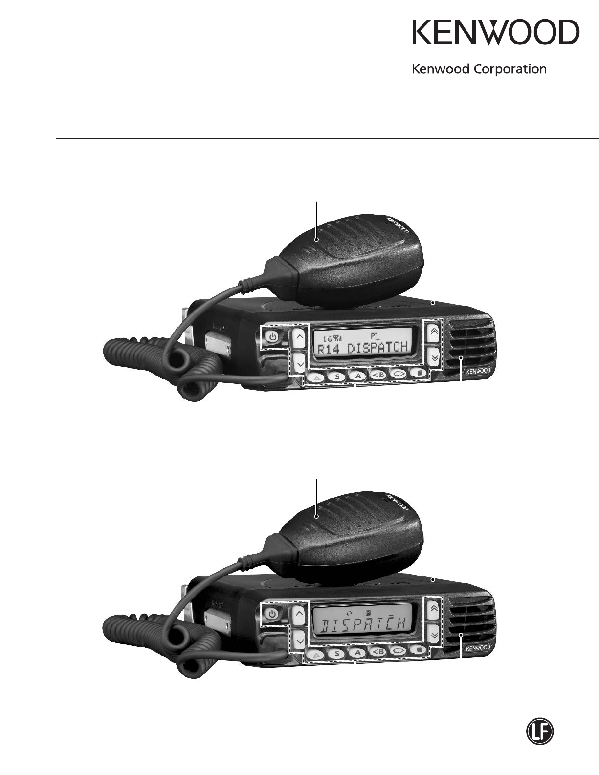
TK-7180H K
Microphone
(T91-0639-05)
© 2005-8 PRINTED IN JAPAN
B51-8736-00 (N) 828
Metallic cabinet
(A01-2194-11)
TK-7182H K
Key top
(K29-9349-01)
Microphone
(T91-0639-05)
Key top
(K29-9349-01)
Panel assy
(A62-1094-23)
Metallic cabinet
(A01-2194-11)
Panel assy
(A62-1094-23)
This product uses Lead Free solder.

TK-7180H/7182H
CONTENTS / GENERAL
GENERAL .................................................................. 2
SYSTEM SET-UP
TK-7180H ............................................................... 4
TK-7182H ............................................................... 5
REALIGNMENT ......................................................... 6
INSTALLATION ......................................................... 9
DISASSEMBLY FOR REPAIR ................................. 16
CIRCUIT DESCRIPTION .......................................... 19
SEMICONDUCTOR DATA ...................................... 24
COMPONENTS DESCRIPTION .............................. 27
PARTS LIST ............................................................. 29
EXPLODED VIEW
TK-7180H ............................................................. 40
TK-7182H ............................................................. 41
PACKING ................................................................. 42
ADJUSTMENT
TK-7180H ............................................................. 43
TK-7182H ............................................................. 55
TERMINAL FUNCTION ........................................... 66
PC BOARD
DISPLAY UNIT (X54-3480-10) : TK-7180H ......... 72
DISPLAY UNIT (X54-3540-10) : TK-7182H ......... 74
TX-RX UNIT (X57-6980-XX) (A/3, C/3).............. 76
TX-RX UNIT (X57-6980-XX) (B/3) ...................... 78
SCHEMATIC DIAGRAM
DISPLAY UNIT (X54-3480-10) : TK-7180H ......... 82
DISPLAY UNIT (X54-3540-10) : TK-7182H ......... 84
TX-RX UNIT (X57-6980-XX) ............................... 86
INTERCONNECTION DIAGRAM
TK-7180H ............................................................. 96
TK-7182H ............................................................. 97
BLOCK DIAGRAM
TK-7180H ............................................................. 98
TK-7182H ........................................................... 100
LEVEL DIAGRAM .................................................. 102
OPTIONAL ACCESSORIES
KRK-10
KAP-2 (Horn Alert/P.A. Relay unit) ................. 109
KCT-40 (Radio Interface Cable)........................ 109
KCT-46 (Ignition Sense Cable) ......................... 109
KMC-35 (Microphone) ...................................... 109
KMC-36 (Keypad Microphone) ........................ 109
SPECIFICATIONS ................................. BACK COVER
(Control Head Remote Kit: 23ft/7m) ....
104
INTRODUCTION
SCOPE OF THIS MANUAL
This manual is intended for use by experienced technicians familiar with similar types of commercial grade communications equipment. It contains all required service information for the equipment and is current as of this publication
date. Changes which may occur after publication are covered
by either Service Bulletins or Manual Revisions, which are
issued as required.
ORDERING REPLACEMENT PARTS
When ordering replacement parts or equipment information, the full part identification number should be included.
This applies to all parts : components, kits, and chassis. If the
part number is not known, include the chassis or kit number
of which it is a part and a sufficient description of the required
component for proper identification.
PERSONAL SAFETY
The following precautions are recommended for personal
safety :
•DONOT transmit if someone is within two feet (0.6
meter) of the antenna.
•DONOT transmit until all RF connectors are secure and
any open connectors are properly terminated.
• SHUT OFF this equipment when near electrical blasting
caps or while in an explosive atmosphere.
• All equipment should be properly grounded before power-
up for safe operation.
• This equipment should be serviced by only qualified tech-
nicians.
PRE-INSTALLATION CONSIDERATIONS
1. UNPACKING
Unpack the radio from its shipping container and check for
accessory items. If any item is missing, please contact
KENWOOD immediately.
2. LICENSING REQUIREMENTS
Federal regulations require a station license for each radio
installation (mobile or base) be obtained by the equipment
owner. The licensee is responsible for ensuring transmitter
power, frequency, and deviation are within the limits permitted by the station license.
Transmitter adjustments may be performed only by a licensed technician holding an FCC first, second or general
class commercial radiotelephone operator’s license. There is
no license required to install or operate the radio.
2
GENERAL
TK-7180H/7182H
3. PRE-INSTALLATION CHECKOUT
3-1. Introduction
Each radio is adjusted and tested before shipment. However, it is recommended that receiver and transmitter operation be checked for proper operation before installation.
3-2. Testing
The radio should be tested complete with all cabling and
accessories as they will be connected in the final installation.
Transmitter frequency, deviation, and power output should
be checked, as should receiver sensitivity, squelch operation,
and audio output. Signaling equipment operation should be
verified.
4. PLANNING THE INSTALLATION
4-1. General
Inspect the vehicle and determine how and where the radio antenna and accessories will be mounted.
Plan cable runs for protection against pinching or crushing
wiring, and radio installation to prevent overheating.
4-2. Antenna
The favored location for an antenna is in the center of a
large, flat conductive area, usually at the roof center. The
trunk lid is preferred, bond the trunk lid and vehicle chassis
using ground straps to ensure the lid is at chassis ground.
4-3. Radio
The universal mount bracket allows the radio to be
mounted in a variety of ways. Be sure the mounting surface
is adequate to support the radio’s weight. Allow sufficient
space around the radio for air cooling. Position the radio close
enough to the vehicle operator to permit easy access to the
controls when driving.
5. INSTALLATION PLANNING – CONTROL STATIONS
5-1. Antenna system
Control station. The antenna system selection depends on
many factors and is beyond the scope of this manual. Your
KENWOOD dealer can help you select an antenna system
that will best serve your particular needs.
5-2. Radio location
Select a convenient location for your control station radio
which is as close as practical to the antenna cable entry point.
Secondly, use your system’s power supply (which supplies
the voltage and current required for your system). Make sure
sufficient air can flow around the radio and power supply to
allow adequate cooling.
SERVICE
This radio is designed for easy servicing. Refer to the
schematic diagrams, printed circuit board views, and alignment procedures contained in this manual.
NOTE
• If you do not intend to use the speaker 3.5-mm jack and
the D-sub 25-pin connector, fit the supplied speaker-jack
cap and D-sub cap to stop dust and sand from getting in.
• If the transceiver is turned ON or OFF when the power-on/
off status message is enabled, the transceiver sends the
status.
4-4. DC Power and wiring
1. This radio may be installed in negative ground electrical
systems only. Reverse polarity will cause the cable fuse to
blow. Check the vehicle ground polarity before installation
to prevent wasted time and effort.
2. Connect the positive power lead directly to the vehicle
battery positive terminal. Connecting the Positive lead to
any other positive voltage source in the vehicle is not recommended.
3. Connect the ground lead directly to the battery negative
terminal.
4. The cable provided with the radio is sufficient to handle
the maximum radio current demand. If the cable must be
extended, be sure the additional wire is sufficient for the
current to be carried and length of the added lead.
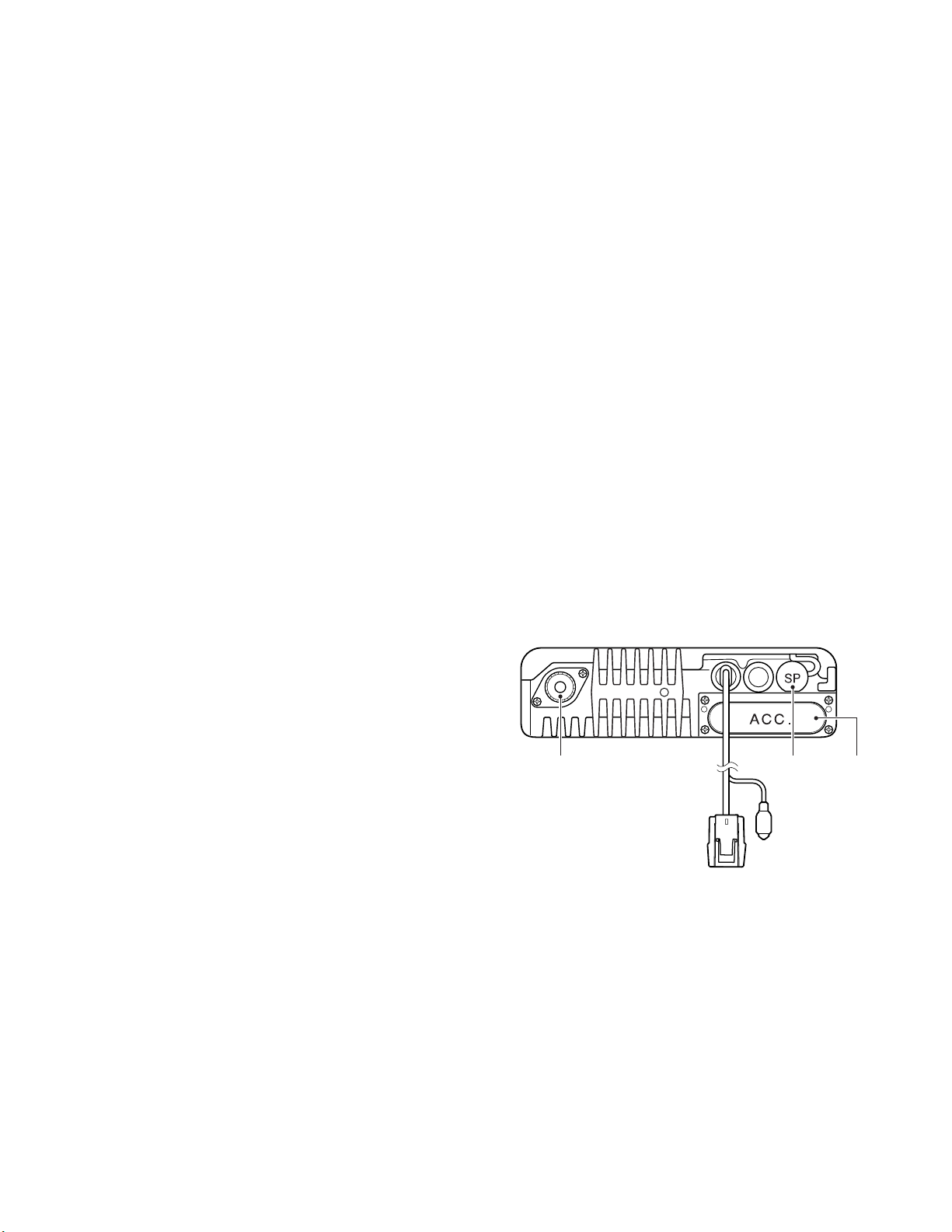
Antenna
connector
Power input
connector
Speaker
jack cap
Ignition
sense cable
D-sub
cap
3
TK-7180H/7182H
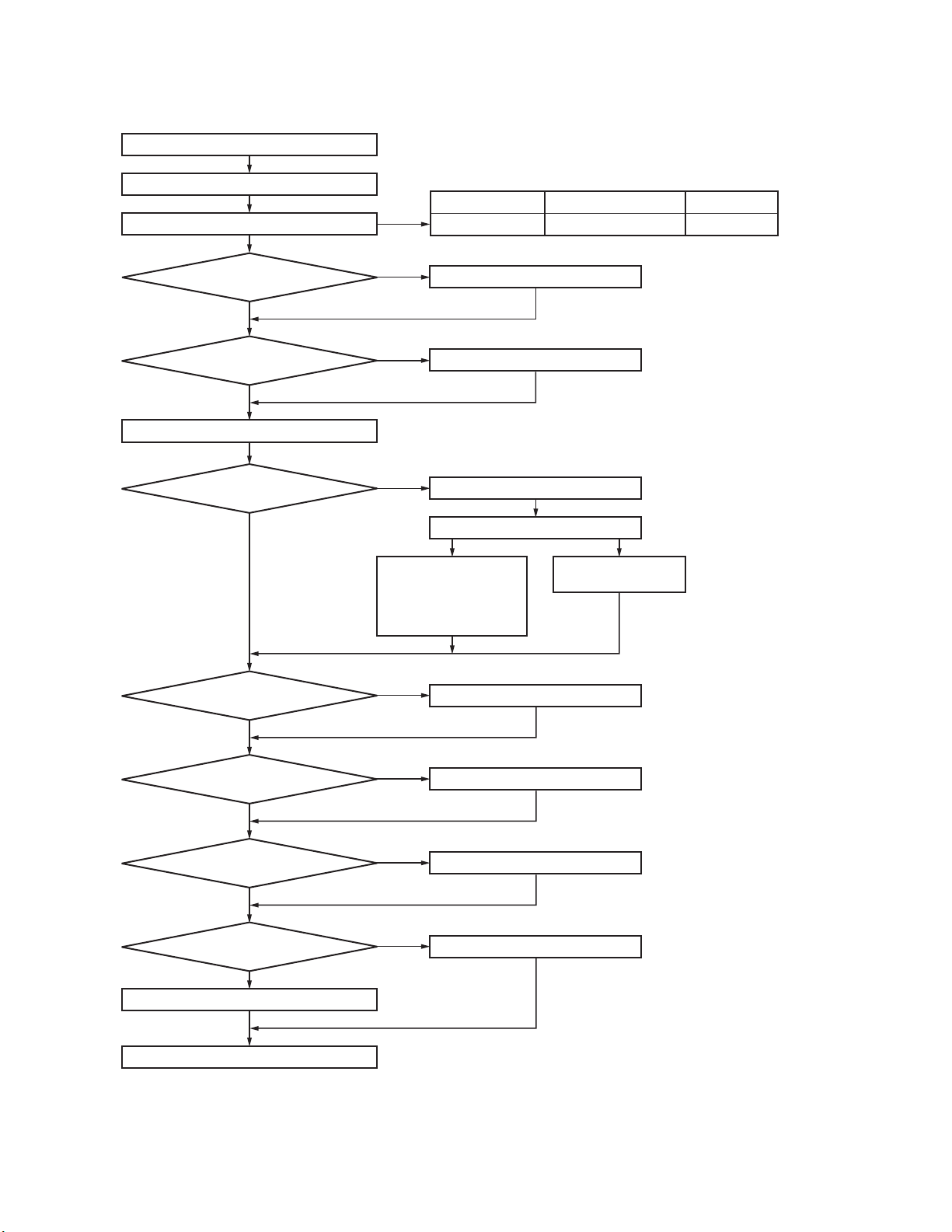
SYSTEM SET-UP (TK-7180H)
Merchandise received
License and frequency allocated by FCC
Choose the type of transceiver
Frequency range RF power Type
136~174MHz 50W TK-7180H K
Are you using
the remote kit?
NO
Are you using
the ignition sense cable?
NO
Transceiver programming
Are you using
the radio interface cable?
NO
Are you using
the public address?
NO
YES
YES
See page 6.
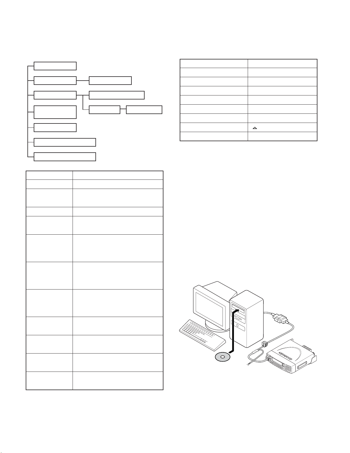
A personal computer (IBM PC or compatible), programming
interface (KPG-46), and programming software (KPG-89D)
are required for programming.
YES
KCT-36 Extension cable
KGP-2A
Modem GPS receiver
or
KGP-2B
Modem GPS controller
YES
KRK-10
KCT-46
KCT-40
(Option)
or
Mobile data terminal
KAP-2
(Option)
(Option)
(Option)
KDS-100
(Option)
See page 11.
See page 9.
See page 9.
(Option)
(Option)
See page 10.
Are you using
the voice guide & storage
unit?
NO
Are you using
the external speaker?
NO
Are you using
the keypad microphone?
NO
Supplied microphone
Delivery
YES
YES
YES
VGS-1
KES-3 or KES-5
KMC-32 or KMC-36
Desk top microphone KMC-9C
(Option)
(Option)
(Option)
See page 12.
See page 13.
When the KAP-2 is installed
in the transceiver, the KES-5
can be installed.
4
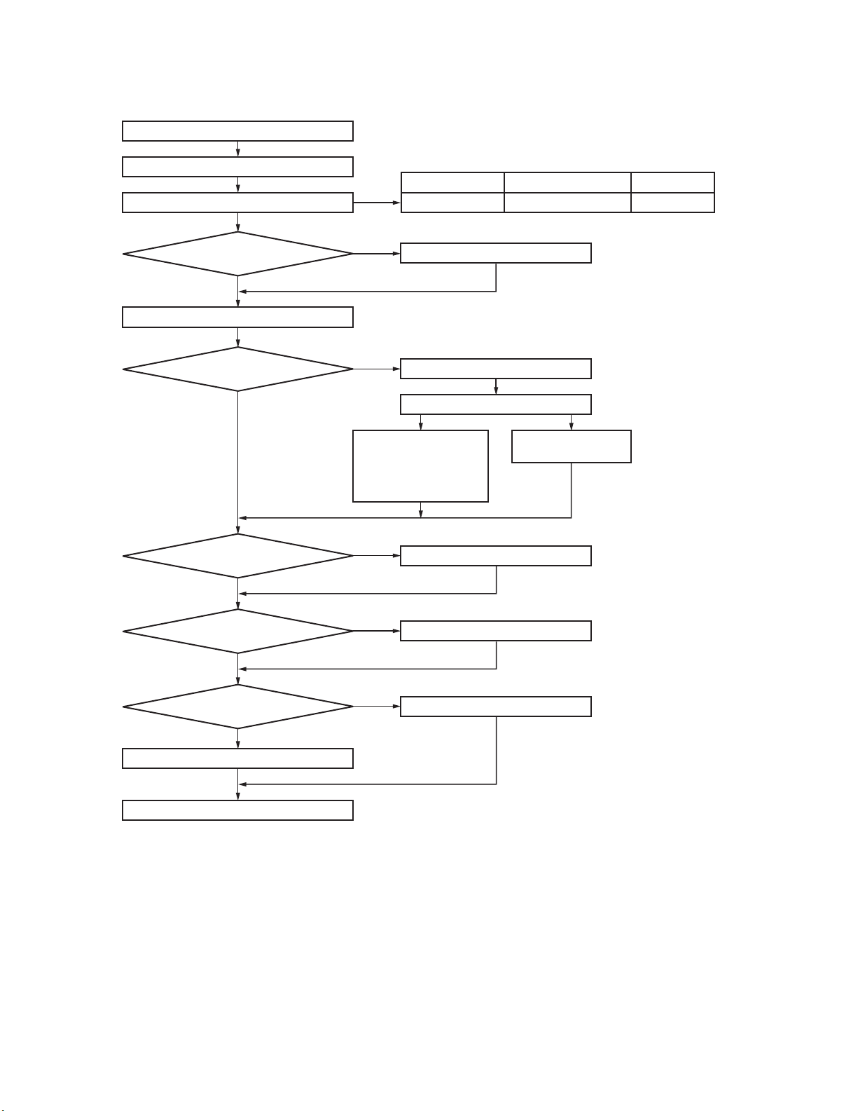
SYSTEM SET-UP (TK-7182H)
Merchandise received
License and frequency allocated by FCC
Choose the type of transceiver
TK-7180H/7182H
Frequency range RF power Type
136~174MHz 50W TK-7182H K
Are you using
the ignition sense cable?
NO
Transceiver programming
Are you using
the radio interface cable?
NO
Are you using
the public address?
NO
Are you using
the external speaker?
NO
YES
See page 6.
A personal computer (IBM PC or compatible), programming
interface (KPG-46), and programming software (KPG-89D)
are required for programming.
YES
KCT-36 Extension cable
KGP-2A
Modem GPS receiver
or
KGP-2B
Modem GPS controller
YES
YES
KCT-46
KCT-40
or
(Option)
KAP-2
KES-3 or KES-5
(Option)
(Option)
KDS-100
Mobile data terminal
(Option)
(Option)
See page 9.
See page 9.
(Option)
(Option)
See page 10.
See page 13.
When the KAP-2 is installed
in the transceiver, the KES-5
can be installed.
Are you using
the keypad microphone?
NO
Supplied microphone
Delivery
YES
KMC-32 or KMC-36
(Option)
Desk top microphone KMC-9C
5
TK-7180H/7182H
KPG-89D
IBM PC
TK-7180H/7182H
KPG-46 or
KPG-46 +
Tuning cable
(E30-3383-05)
REALIGNMENT
1. Modes
User mode
Panel test mode
PC mode
Firmware
programming mode
Clone mode
Firmware version information
Clock adjustment mode *1
Mode Function
User mode For normal use.
Panel test mode Used by the dealer to check the funda-
Panel tuning mode
PC mode Used for communication between the
Data programming Used to read and write frequency data
mode and other features to and from the
PC test mode Used to check the transceiver using the
PC tuning mode
Firmware Used when changing the main program
programming mode of the flash memory.
Clone mode Used to transfer programming data from
Firmware version Used to confirm the internal firmware
information version.
Clock adjustment Used by the dealer to adjust date and
mode *1 time.
*1 : TK-7180H only
Panel tuning mode
Data programming mode
PC test mode
mental characteristics.
Used by the dealer to tune the transceiver.
transceiver and PC (IBM compatible).
transceiver.
PC. This feature is included in the FPU.
See panel test.
Used to tune the transceiver using the PC.
This feature is included in the FPU.
See panel tuning.
one transceiver to another.
PC tuning mode
2. How to Enter Each Mode
Mode Operation
User mode Power ON
Panel test mode [A] + Power ON
PC mode Received commands from PC
Panel tuning mode [Panel test mode] + [S]
Firmware programming mode [S] + Power ON
Clone mode [B] + Power ON
Firmware version information [ ] + Power ON
Clock adjustment mode *2 [C] + Power ON
*2 : TK-7180H only
3. Panel Test Mode
Setting method refer to ADJUSTMENT.
4. Panel Tuning Mode
Setting method refer to ADJUSTMENT.
5. PC Mode
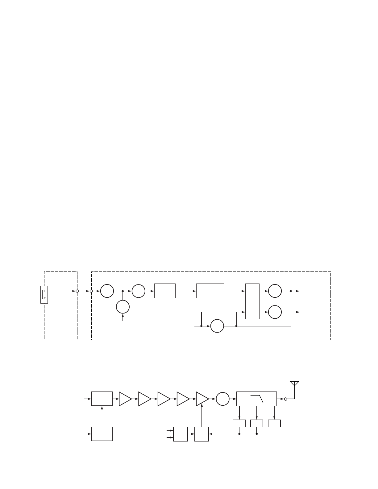
5-1. Preface
The transceiver is programmed by using a personal computer, programming interface (KPG-46) and programming
software (KPG-89D).
The programming software can be used with an IBM PC
or compatible. Figure 1 shows the setup of an IBM PC for
programming.
Fig. 1
6

REALIGNMENT
TK-7180H/7182H
5-2. Connection procedure
1. Connect the transceiver to the personal computer with
the interface cable.
2. When the POWER switch on, user mode can be entered
immediately. When PC sends command the transceiver
enter PC mode, and “PROGRAM” is displayed on the
LCD.
When data transmitting from transceiver, the red LED is
lights.
When data receiving to transceiver, the green LED is
lights.
Note:
The data stored in the personal computer must match
model type, when it is written into the flash memory.
5-3. KPG-46 description
(PC programming interface cable: Option)
The KPG-46 is required to interface the transceiver to the
computer. It has a circuit in its D-sub connector (25-pin) case
that converts the RS-232C logic level to the TTL level.
The KPG-46 connects the modular microphone jack of the
transceiver to the computers RS-232C serial port.
5-4. Programming software KPG-89D description
The KPG-89D is the programming software for the trans-
ceiver supplied on a CD-ROM. This software runs under MSWindows 98, ME, Windows 2000 or XP on an IBM-PC or
compatible machine.
The data can be input to or read from the transceiver and
edited on the screen. The programmed or edited data can be
printed out. It is also possible to tune the transceiver.
6. Firmware Programming Mode
6-1. Preface
Flash memory is mounted on the transceiver. This allows
the transceiver to be upgraded when new features are released in the future. (For details on how to obtain the firmware, contact Customer Service.)
6-2. Connection procedure
Connect the transceiver to the personal computer (IBM
PC or compatible) with the interface cable (KPG-46). (Connection is the same as in the PC Mode.)
Note :
You can only program firmware from the 8-pin micro-
phone connector on the front panel. Using the 25-pin logic
interface on the rear panel will not work.
6-3. Programming
1. Start up the firmware programming software (Fpro.exe).
2. Set the communications speed (normally, 115200 bps)
and communications port in the configuration item.
3. Set the firmware to be updated by File name item.
4. Press and hold the [S] key while turning the transceiver
power ON. Then, the orange LED on the transceiver lights
and “PROG 115200” (TK-7180H) or “PROG1152” (TK7182H) is displayed.
5. Check the connection between the transceiver and the
personal computer, and make sure that the transceiver is
in the Program mode.
6. Press write button in the window. When the transceiver
starts to receive data, “PG” is blinking (TK-7180H) or
“LOADING” is displayed (TK-7182H).
7. If writing ends successfully, the checksum is calculated
and a result is displayed.
8. If you want to continue programming other transceivers,
repeat steps 4 to 7.
Note:
This mode cannot be entered if the Firmware Programming mode is set to Disable in the Programming software.
6-4. Function
1. If you press the [■ ] key while “PROG 115200” (TK7180H) or “PROG1152” (TK-7182H) is displayed, the display changes to “PROG 19200” (TK-7180H) or “PROG
192” (TK-7182H) (The LED blinks green) to indicate that
the write speed is low speed (19200 bps). If you press the
[■] key again while “PROG 19200” (TK-7180H) or “PROG
192” (TK-7182H) is displayed, the display changes to
“PROG 38400” (TK-7180H) or “PROG 384” (TK-7182H)
(The LED lights red and orange alternatively). If you press
the [■ ] key again while “PROG 38400” (TK-7180H) or
“PROG 384” (TK-7182H) is displayed, the display changes
to “PROG 57600” (TK-7180H) or “PROG 576” (TK-7182H)
(The LED blinks orange). If you press the [■] key again
while “PROG 57600” (TK-7180H) or “PROG 576” (TK7182H) is displayed, the display returns to “PROG
115200” (TK-7180H) or “PROG1152” (TK-7182H) (The
LED lights orange).
2. If you press the [
7180H) or “PROG1152” (TK-7182H) is displayed, the
checksum is calculated, and a result is displayed. If you
press the [
“PROG 115200” (TK-7180H) or “PROG1152” (TK-7182H)
is redisplayed.
] key again while the checksum is displayed,
] key while “PROG 115200” (TK-
Note:
Normally, write in the high-speed mode.
7
TK-7180H/7182H
Cloning cable
(E30-3382-05)
REALIGNMENT
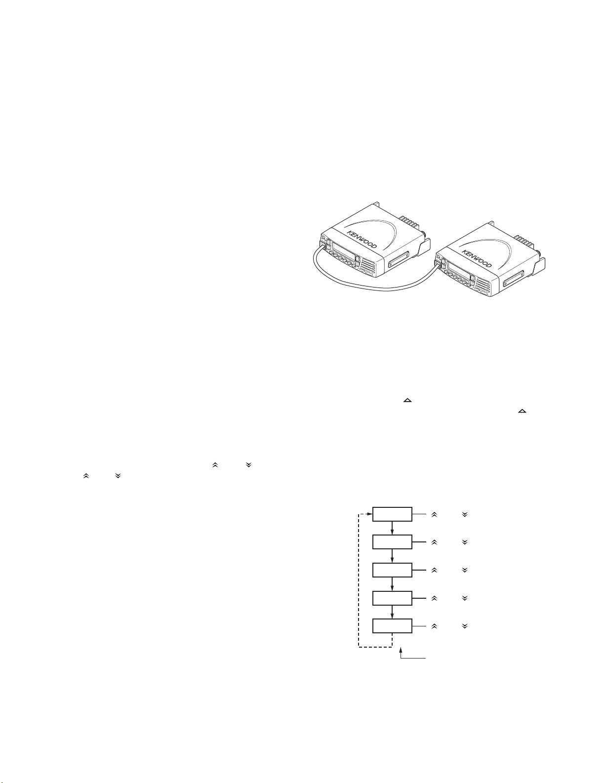
7. Clone Mode
Programming data can be transferred from one transceiver to another by connecting them via their 8-pin microphone connectors. The operation is as follows (the transmit
transceiver is the master and the receive transceiver is a
slave).
The following data cannot be cloned.
• Tuning data
• Embedded message with password
• Model name data
• ESN (Electronic Serial Number) data
1. Press and hold the [B] key while turning the transceiver
power ON. If the read authorization password is set to the
transceiver, “CLONE LOCK” (TK-7180H) or “CLN LOCK”
(TK-7182H) is displayed. If the password is not set,
“CLONE MODE” (TK-7180H) or “CLONE” (TK-7182H) is
displayed.
2. When you enter the correct password, and “CLONE
MODE” (TK-7180H) or “CLONE” (TK-7182H) is displayed,
the transceiver can be used as the cloning master. The
following describes how to enter the password.
3.
How to enter the password with the microphone keypad;
•
If one of keys 0 to 9 is pressed while “CLONE LOCK” (TK-
7180H) or “CLN LOCK” (TK-7182H) is displayed, the
pressed number is displayed on the LCD. Each press of
the key shifts the display in order to the left. When you
enter the password and press the [
MODE” (TK-7180H) or “CLONE” (TK-7182H) is displayed
if the entered password is correct. If the password is in-
correct, “CLONE LOCK” (TK-7180H) or “CLN LOCK” (TK-
7182H) is redisplayed.
• How to enter the password with the [
If the [
(TK-7180H) or “CLN LOCK” (TK-7182H) is displayed, the
number (0 to 9) blinks on the LCD. When you press the [C]
key, the currently selected number is determined. If you
press the [A] key, the least digit of the password is de-
leted. If you press the [S] key after entering the password
in this procedure, “CLONE MODE” (TK-7180H) or
“CLONE” (TK-7182H) is displayed if the entered pass-
word is correct. If the password is incorrect, “CLONE
LOCK” (TK-7180H) or “CLN LOCK” (TK-7182H) is
redisplayed.
4. Power on the slave transceiver.
5. Connect the cloning cable (Part No. E30-3382-05) to the
modular microphone jacks on the master and slave.
6. Press the [S] key on the master while the master displays
“CLONE MODE” (TK-7180H) or “CLONE” (TK-7182H).
The data of the master is sent to the slave. While the
slave is receiving the data, “PROGRAM” is displayed.
When cloning of data is completed, the master displays
“END”, and the slave automatically operates in the User
mode. The slave can then be operated by the same pro-
gram as the master.
] and [ ] keys is pressed while “CLONE LOCK”
] key, “CLONE
*
] and [ ] keys;
7. The other slave can be continuously cloned. When the [S]
key on the master is pressed while the master displays
“END”, the master displays “CLONE MODE” (TK-7180H)
or “CLONE” (TK-7182H). Carry out the operation in step 4
to 6.
Notes:
• Only the same models can be cloned together.
• Cannot be cloned if the overwrite password is programmed to the slave.
Fig. 2
8. Firmware Version Information
Press and hold the [ ] key while turning the transceiver
power ON and then keep pressing and holding the [
the firmware version information appears on the LCD.
9.
Clock Adjustment Mode (TK-7180H only)
9-1. Flow chart of operation
[C] + Power ON
YEAR
[S]
MONTH
[S]
DAY
[S]
HOUR
[S]
MINUTE
[S]
[ ] and [ ] keys
[ ] and [ ] keys
[ ] and [ ] keys
[ ] and [ ] keys
[ ] and [ ] keys
Completion
] key,
8

INSTALLATION
KDS-100, KGP-2A,
KGP-2B or through
KCT-36 extension cable
q
e
w
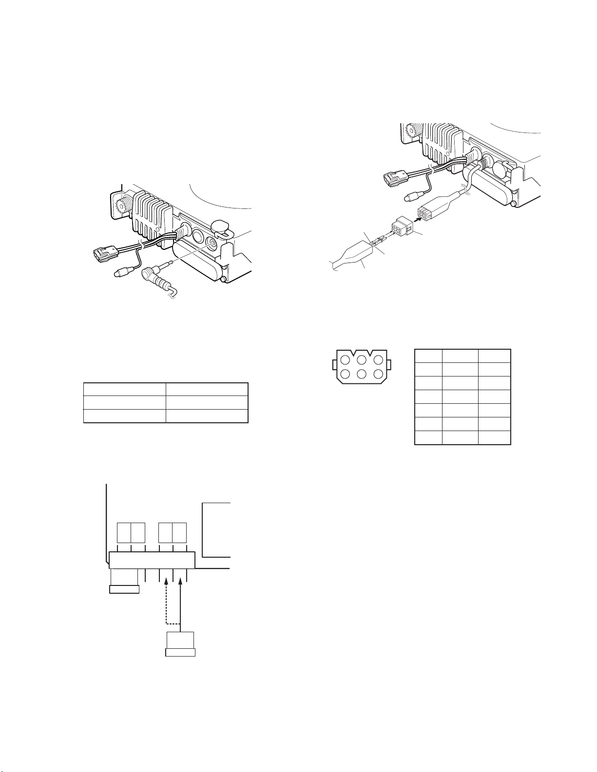
1. Ignition Sense Cable (KCT-46 : Option)
The KCT-46 is an optional cable for enabling the ignition
function. The ignition function lets you turn the power to the
transceiver on and off with the car ignition key.
1-1. Connecting the KCT-46 cable to the transceiver
1. Open the KCT-46 fuse holder and insert a mini blade fuse
(3A). ( q )
2. While holding a clear protective cover, remove the black
cap at the end of the yellow cable (ignition sense cable) of
the transceiver. ( w )
3. Connect the plug of the KCT-46 to the yellow cable termi-
nal of the transceiver. ( e )
4. Connect the other end of the KCT-46 to the ignition line of
the car. ( r )
Note : You must setup using the KPG-89D.
TK-7180H/7182H
Fig. 2
w
e
F52-0019-05
q
r
Iginition line
of the car
Fig. 1
2. Radio Interface Cable (KCT-40 : Option)
The KCT-40 connection cable kit is used to connect the
transceiver to the KDS-100 (Mobile data terminal), KGP-2A
(Modem GPS receiver), KGP-2B (Modem GPS controller) or
through the KCT-36 extension cable.
2-1. Connecting the KCT-40 cable to the transceiver
1. Remove the D-sub cap on the rear of the transceiver. ( q )
2. Connect the D-sub connector of the KCT-40 to the D-sub
25-pin terminal of the transceiver. ( w )
3. Connect the 15-pin connector of the KCT-40 to a KDS-100,
KGP-2A, KGP-2B or through a KCT-36 extension cable.
( e )
Note : You must setup using the KPG-89D.
2-2. Terminal function
D-sub 25-pin
Pin No. Function Pin No. Function Function
10 RXD2 14 TXD TXD
11 - ---
12 AIO7 11 MM MM
13 AIO6 6 PTT PTT
14 SB 1 SB SB
15 - ---
16 - ---
17 - ---
18 - ---
19 DEO 4 DI DI
20 AIO5 8 SQ SQ
21 AIO4 10 AM AM
22 AIO3 13 - DISP OFF
23 AIO2 12 - -
24 AIO1 7 DTC DTC
25 - ---
TK-7180H/7182H
1- ---
2- ---
3- ---
4- ---
5DI5DO DO
6- ---
7 GND 3 GND GND
8 AIO8 9 TXS/LOK TXS/LOK
9 TXD2 15 RXD RXD
Molex 15-pin
KDS-100 KGP-2A/2B
9
TK-7180H/7182H
INSTALLATION
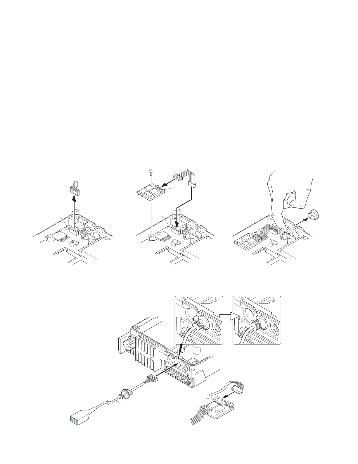
3. Horn Alert/P.A. Relay Unit (KAP-2 : Option)
The Horn alert (max. 2A drive), Public address and External
speaker function are enabled by installing the KAP-2 in the
transceiver.
3-1. Installing the KAP-2 unit in the transceiver
(The kit A is not used in the KAP-2 accessories)
1. Remove the cabinet, top packing and shielding plate of the
transceiver.
2. Set the KAP-2 relay unit jumper pins according to the purpose of use.
3. Remove the 6-pin jumper connector inserted in the TX-RX
unit (B/3) connector (CN428). ( q )
4. Insert one side of the lead wire with connector (E37-1114-
05) into the relay unit connector (CN3) ( w ) and the other
side into the TX-RX unit (B/3) connector (CN428) ( e ).
5. Place the relay unit at the position shown in Figure 3-2 and
secure it to the chassis with a screw.
6. Remove the cap on the rear of the chassis by pushing it
from the inside with your finger. ( r )
7. Pass the 6-pin connector of the cable (E37-1113-05)
through the chassis hole ( t ) and insert the bush into the
chassis hole.
8. Rotate the bush of the cable 90 degrees counterclockwise
as viewed from the rear of the chassis. ( y )
9. Insert the 6-pin connector of the cable into the connector
(CN2) of the KAP-2 relay unit. ( u )
Note : You must setup using the KPG-89D.
E37-1114-05
w
CN3
e
q
CN428
CN428
Fig. 3-1 Fig. 3-2 Fig. 3-3
y
r
10
E37-1113-05
t
Fig. 3-4
CN2
u
INSTALLATION
CN1
KRK-10 main panel
u
i
4.
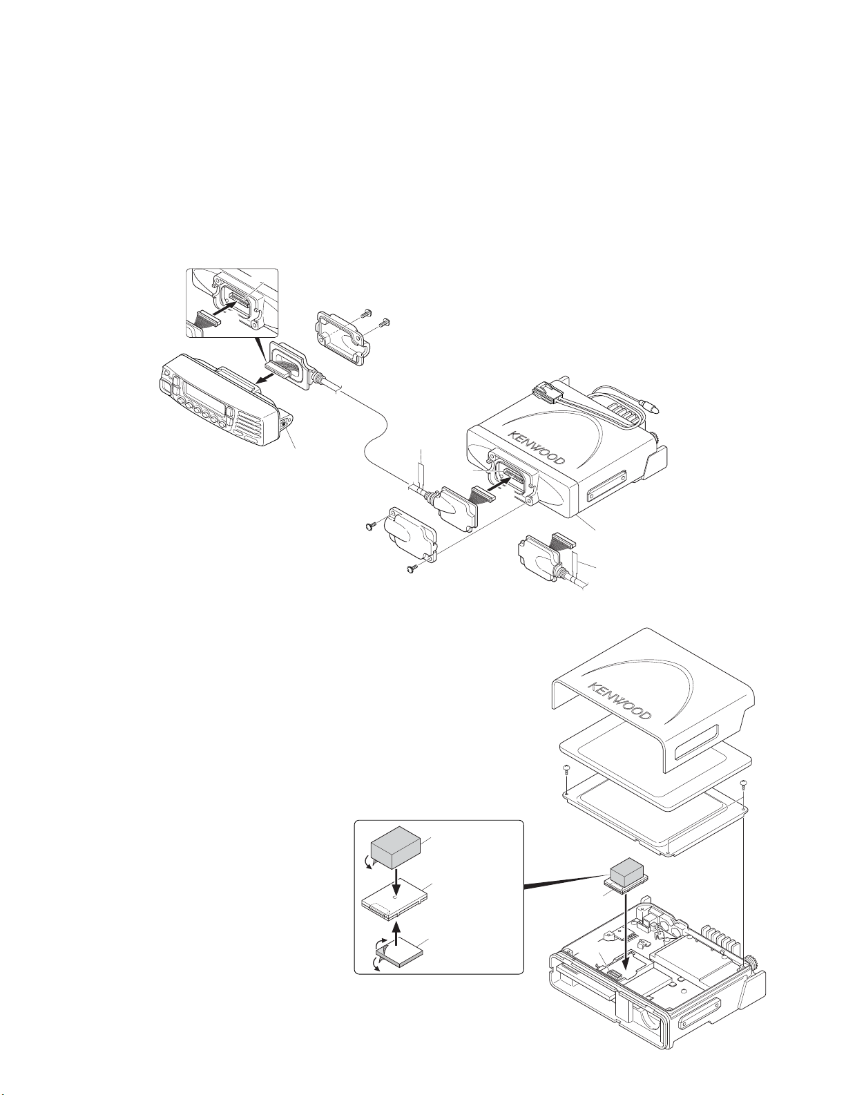
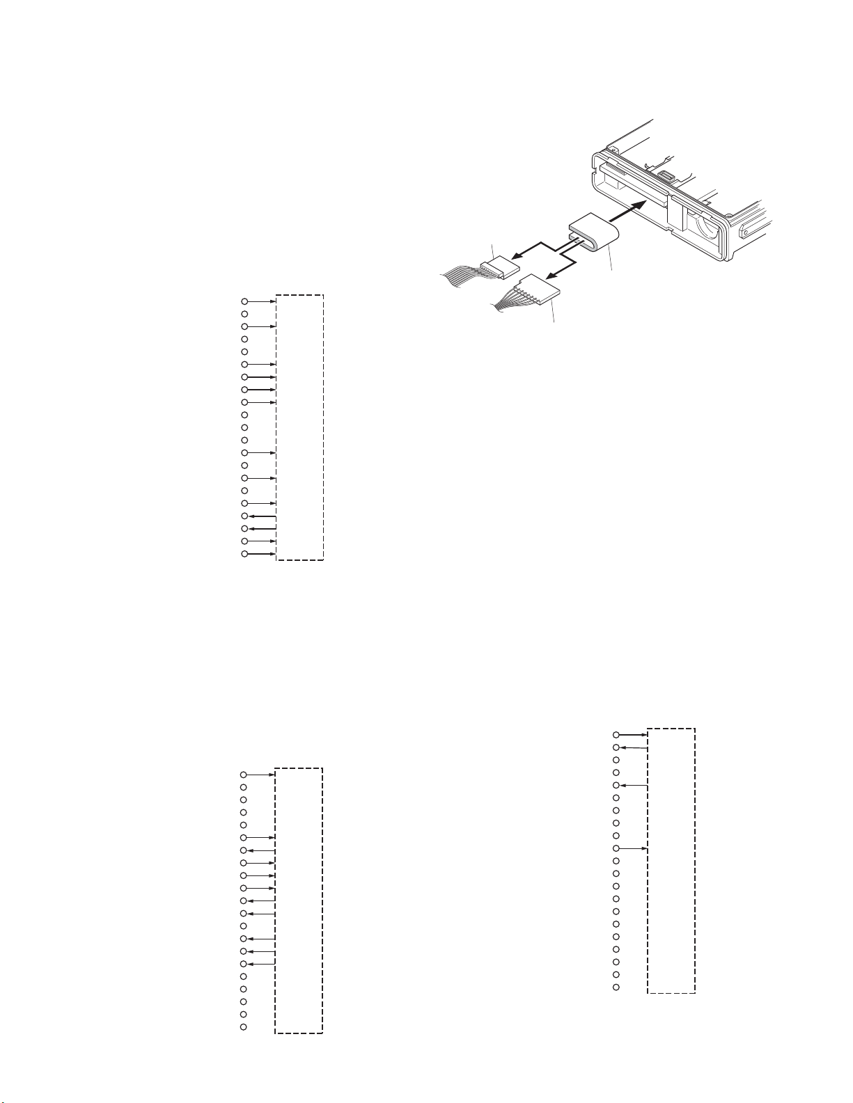
Control Head Remote Kit
(KRK-10 : Option) (TK-7180H only)
The KRK-10 remote kit is used to remotely operate the
transceiver.
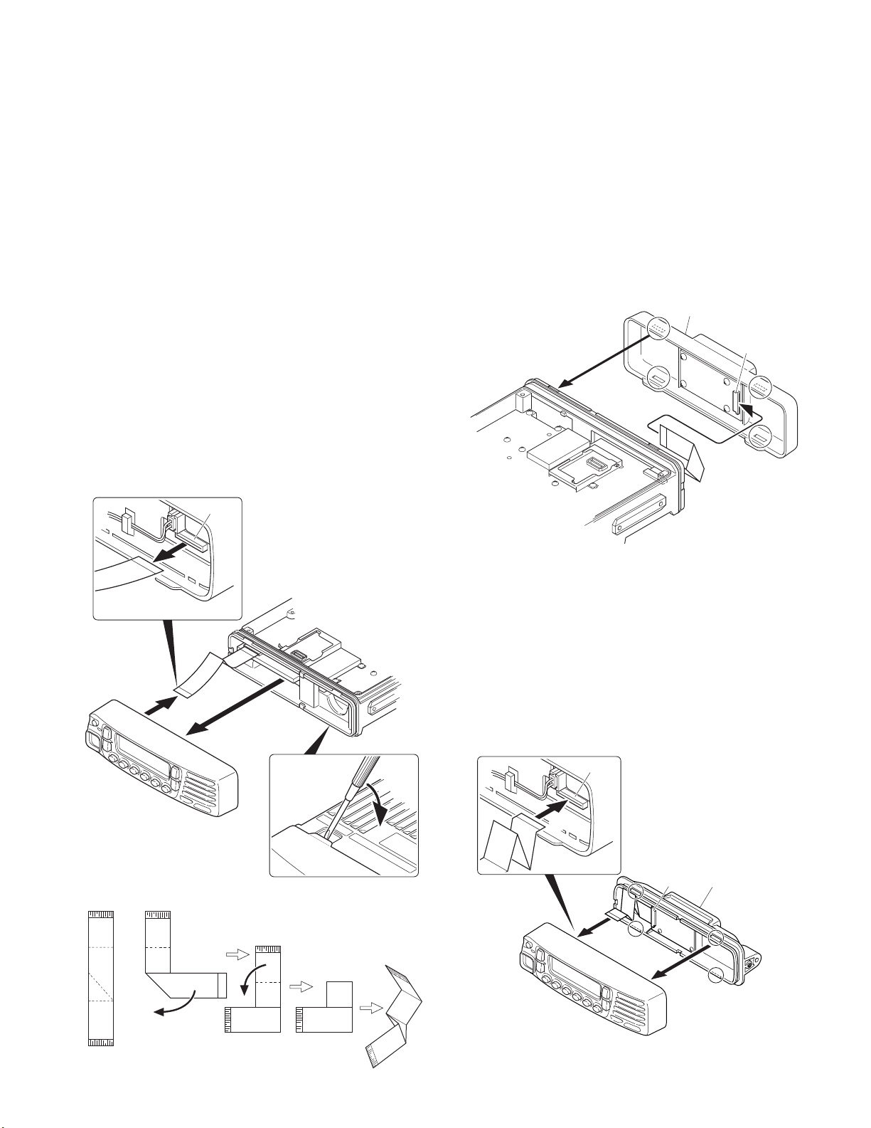
4-1. Installing the KRK-10 kit to the transceiver
1. Remove the front panel from the transceiver.
2. Install the KRK-10 main panel onto the transceiver.
3. Install the KRK-10 rear panel onto the front panel.
4. Connect the KRK-10 main panel to the rear panel with the
cable.
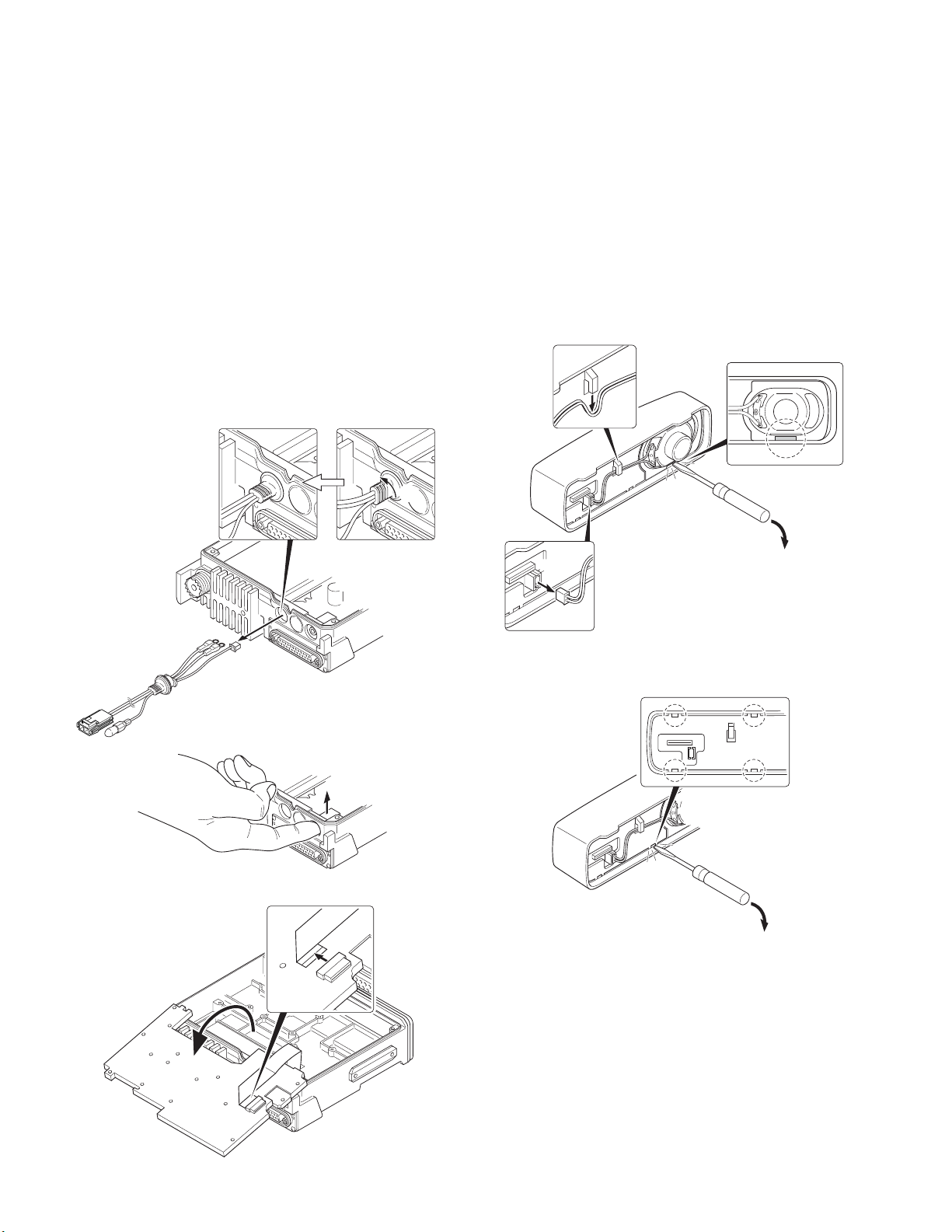
■ Remove the front panel from the transceiver
1. Lift the two tabs of the panel on the bottom of the transceiver with a flat-head screwdriver ( q ) and remove the
panel from the chassis ( w ).
Note : Confirm that the tabs of the speaker hardware fixture and holder is securely fitted in the front panel.
2. Remove the flat cable from the connector (CN902) of the
display unit of the panel. ( e )
3. Fold the black line of the flat cable (in three parts) as
shown in Figure 4-2. ( r, t, y )
TK-7180H/7182H
■
Install the KRK-10 main panel onto the transceiver
4. Insert the flat cable that was removed in step 2 above into
the connector (CN1) of the interface unit (A/2) of the KRK10 main panel (A62-1101-01). ( u )
Note : The terminal side of the flat cable must face down
when inserting the flat cable into the connector.
5. Fit the main panel with four tabs onto the front of the
chassis. ( i )
Note : When installing the main panel onto the front of the
chassis, hold down the flat cable with your fingers to prevent it from being caught.
Chassis
side
Fig. 4-1
r
CN902
e
w
q
Fig. 4-3
■ Install the KRK-10 rear panel onto the front panel
6. Insert the flat cable attached to the interface unit (B/2) of
the KRK-10 rear panel (A82-0056-11) into the connector
(CN902) of the display unit of the panel ( o ). (The flat
cable has been pre-inserted in the connector (CN2) of the
rear panel at the time of shipping.)
Note : The terminal side of the flat cable must face down
when inserting the flat cable into the connector.
7. Fit the four tabs of the rear panel into the front panel. ( !0 )
CN902
o
CN2
KRK-10 rear panel
y
r
t
Panel
side
t
Fig. 4-2
y
!0
Fig. 4-4
11
TK-7180H/7182H
CN4
CN1
CN403
q
w
Cushion
(G13-1994-04)
20 x 30 x 12 mm
Cushion
(G13-1992-04)
21 x 21 x 2.5 mm
VGS-1
■ Connect the KRK-10 main panel to the rear panel
with the cable
8. Insert one 14-pin connector of the cable (E30-7514-15)
into the connector (CN3) of the interface unit (A/2) of the
main panel. ( !1 )
Note : Insert the connector that has a sticker onto the
cable to the connector of the main panel.
9. Secure the cable bush on the main panel and fit the water-
proof packing (orange) ( !2 ) securely over top.
INSTALLATION
10. Install the molded cover ( !3 ) over the connector on the
main panel and secure it with two screws ( !4 ).
11. Insert the other 14-pin connector of the cable into the
connector (CN4) of the interface unit (B/2) of the rear
panel. ( !5 )
12. Secure the cable bush on the rear panel and fit the waterproof packing (orange) ( !6 ) securely over top.
13. Install the molded cover ( !7 ) over the connector on the
rear panel and secure it with two screws ( !8 ).
!8
!5
!7
!6
KRK-10
rear panel
!4
5. Voice Guide & Storage Unit
(VGS-1 : Option) (TK-7180H only)
5-1. Installing the VGS-1 unit in the transceiver
1. Remove the cabinet, top packing and shielding plate of the
transceiver.
2. Attach two cushions to VGS-1 as shown in Figure 5. ( q )
Note : Be sure not to cover the connector with the bottom
cushion.
3. Insert the VGS-1 connector (CN1) into the TX-RX unit (B/3)
connector (CN403). ( w )
!8
Sticker
!3
!4
Fig. 4-5
Note : A cable can be connected from the left side as shown
in the Figure 4-5 or from right side.
However, the 14-pin connector must be connected to correct
direction.
CN3
!1
!2
KRK-10
main panel
Sticker
!2
(Right side)
Note : You must setup using the KPG-89D.
12
Fig. 5
4
5
Square plug
(E59-0419-05)
Black/White
lead
Black lead
Insulating cover
(F29-0481-05)
INSTALLATION
TK-7180H/7182H
6. External Speaker (Option)
6-1. KES-3
The KES-3 is an external speaker for the 3.5-mm-diameter
speaker jack.
■ Connection Procedure
1. Connect the KES-3 to the 3.5-mm-diameter speaker jack
on the rear of the transceiver.
Fig. 6-1
6-2. KES-5
External speaker KES-5 can be installed for KAP-2. If KES5 is installed, it can be set by changing the CN1 short pin from
pins 4 and 5 to pins 5 and 6 on the KAP-2.
KAP-2 CN1 Connect Set Up
4-5 INT. SP or KES-3
5-6 KES-5
When you use the KES-5, plug the short pin to pins 5 and
6 on the KAP-2.
When you use the INT. SP or KES-3, plug the short pin to
pins 4 and 5 on the KAP-2.
■ Connection Procedure
Insert the crimp terminal into the Square plug supplied
with the KAP-2.
Fig. 6-3
■ KAP-2 Cable (E37-1113-05) 6-pin Connector
321
654
Pin No.
Color Name
1 Red HR2
2 Blue GND
3 Yellow OSP
4 Green ESP
5 Brown GND
6 Black HR1
KAP-2 unit
HR1
KES-3
INT
HR2
CN116
or
EXT
KES-5INT. SP
Short pin
Fig. 6-2
13
TK-7180H/7182H
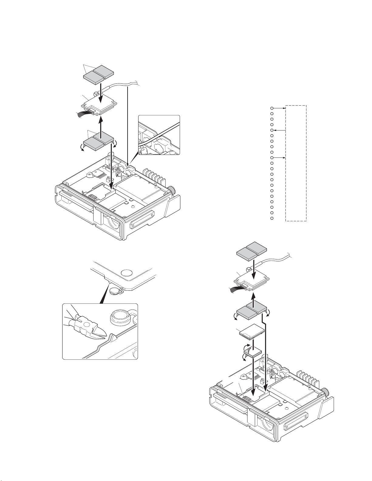
7. Voice Scrambler Board Connection
1. Remove the front panel from the transceiver.
2. Solder each lead of the scrambler board to a necessary
location of each landing on the component side of the TXRX unit (B/3).
3. Wrap the scrambler board in a cushion and install it on the
front of the chassis as shown in Figure 8-2.
Note : You must setup using the KPG-89D.
TX-RX unit (B/3)
Solder land
GND (GND)
RXD1
TXD1 (PTT)
TXD2
OPT1 (CODE SELECT1)
OPT3 (CODE SELECT2)
OPT4 (ECHO PTT)
OPT5 (CODE SELECT8)
OPT2 (SCRAMBLE)
RXEO (RX OUT)
OPT6 (CODE SELECT4)
8. ANI Board Connection
1. Remove the front panel from the transceiver.
2. Solder each lead of the scrambler board to a necessary
location of each landing on the component side of the TXRX unit (B/3).
3. Wrap the scrambler board in a cushion and install it on the
front of the chassis as shown in Figure 8-2.
Note : You must setup using the KPG-89D.
OPT1 (CH BUSY)
OPT5 (EMERGENCY)
DTI (DATA OUT)
TCTL (TONE CTRL)
AUDIH (AUDIO INHIB)
OPT2 (AUX I/O)
STON (SIDE TONE)
RXD2
DTI
TCTL
TXO (TX OUT)
AUDIH
STON
TXI (TX IN)
RXEI (RX IN)
8C (+V)
Fig. 7
TX-RX unit (B/3)
Solder land
GND (A–)
RXD1
TXD1
TXD2
RXD2
OPT3 (KEY)
OPT4 (PTT)
5E (A+)
TXO
RXEO
TXI
RXEI
OPT6
8C
5E
Voice scrambler board
ANI board
INSTALLATION
ANI board
9. GPS Receiver Connection
9-1. Installing the GPS receiver
1. Remove the cabinet, top packing and shielding plate of the
transceiver.
2. Remove the front panel from the transceiver.
3. Attach two cushions to the top of the GPS receiver.
4. Attach the GPS receiver to the shield case with two cushions as shown in Figure 9-2.
5. Solder each lead of the GPS receiver to a necessary location of each landing on the component side of the TX-RX
unit (B/3).
6. Place the GPS antenna cable in the hollow at the rear of
the chassis. (Fig. 9-2 q )
Note : If the GPS receiver is installed, cut the base of the
convex tab of the top packing with a pair of nippers, or
similar tool. (Fig. 9-3 w )
If the convex tab of the top packing is cut off, the water
proofing property is no longer guaranteed.
Note : You must setup using the KPG-89D.
*1 : Depending on the connected optional accessory, the
DATA OUT1 may connect to either RXD1 or RXD2.
3M double coated cushion
No. 4008 (or No.4408)
25 x 110 mm
Voice scrambler board
Fig. 8-2
TX-RX unit (B/3)
Solder land
RXD1 (DATA OUT1)*
GND (GND)
RXD2 (DATA OUT1)*
TXD1
TXD2
OPT1
OPT3
OPT4
OPT5
5E (+5V)
DTI
TCTL
TXO
AUDIH
OPT2
STON
RXEO
TXI
RXEI
OPT6
1
1
8C
GPS receiver
14
Fig. 8-1
Fig. 9-1
INSTALLATION
TX-RX unit (B/3)
Solder land
GND (GND)
RXD1
TXD1
TXD2
RXD2 (DATA OUT1)
OPT1
OPT3
OPT4
OPT5
5E (+5V)
DTI
TCTL
TXO
AUDIH
OPT2
STON
RXEO
TXI
RXEI
OPT6
8C
GPS receiver
TK-7180H/7182H
3M Double coated cushion
No. 4016 (or No. 4416)
30 x 25 mm
GPS receiver
3M Double coated cushion
No. 4016 (or No. 4416)
30 x 25 mm
4. Insert the VGS-1 connector (CN1) into the TX-RX unit (B/3)
connector (CN403).
5. Perform step 3 to 6 of “9-1. Installing the GPS receiver”
described on page 14.
Note : You must setup using the KPG-89D.
q
Fig. 9-4
Fig. 9-2
w
Fig. 9-3
9-2. Installing the GPS receiver together with the
VGS-1 (TK-7180H only)
1. Remove the cabinet, top packing and shielding plate of the
transceiver.
2. Remove the front panel from the transceiver.
3. Attach a cushion to the bottom of the VGS-1 as shown in
Figure 9-5.
Note : Be sure not to cover the connector with the cushion.
GPS receiver
VGS-1
CN1
CN403
Fig. 9-5
15
TK-7180H/7182H
DISASSEMBLY FOR REPAIR
1. Precautions on Disassembly
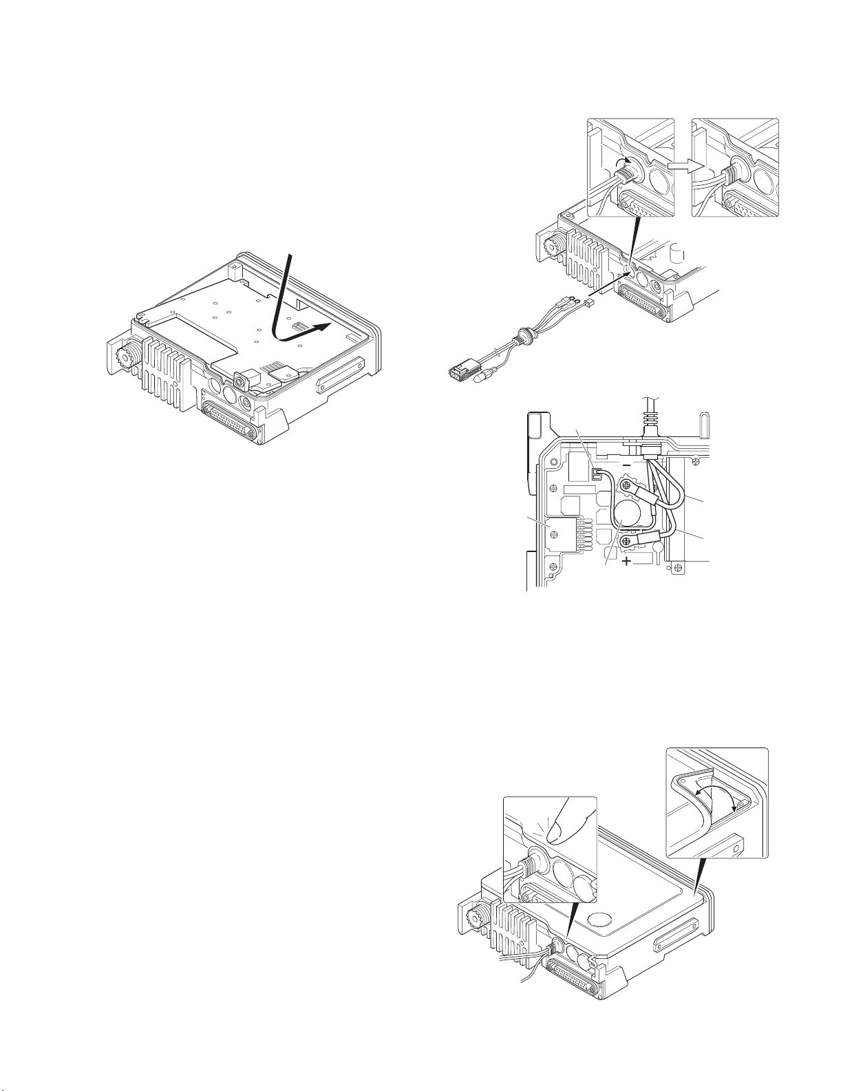
■ TX-RX PCB (TX-RX unit B/3) Disassembly
1. Remove all screws and antenna terminals on the TX-RX
PCB.
2. Rotate the bush of the power supply cable 90 degrees
counterclockwise as viewed from the rear of the chassis
( q ) and remove the power supply cable from the chassis
( w ).
3. When the speaker phone jack is pushed up, using your
finger, from the rear of the chassis ( e ), the TX-RX PCB is
removed from the chassis.
Note : The TX-RX PCB and D-sub PCB (TX-RX unit A/3) are
connected with a flat cable. Remove them carefully.
4. Turn the TX-RX PCB over and remove the flat cable from
the connector (CN427). ( r )
5. Remove the TX-RX PCB from the chassis.
q
■ Removing the speaker hardware fixture
(J21-8481-03) and holder (J19-5485-02)
1. Remove the speaker lead from the holder hook. ( q )
2. Remove the speaker connector from the display unit con-
nector (CN901). ( w )
3. When removing the speaker hardware fixture, insert a flat-
head screwdriver at the position shown in Figure 2-1 and
tilt it in the direction shown by the arrow. ( e )
4. To remove the holder, insert a flat-head screwdriver into
tab of the holder and tilt it in the direction shown by the
arrow. ( r )
q
e
CN901
w
Fig. 1-1
Fig. 1-2
w
Fig. 2-1
e
r
r
Fig. 2-2
16
CN427
Fig. 1-3
q
w
DISASSEMBLY FOR REPAIR
2. Precautions on Reassembly
■ TX-RX PCB (TX-RX unit B/3) Reassembly
1. With the TX-RX PCB turned over, insert the flat cable from
the D-sub PCB (TX-RX unit A/3) into the connector
(CN427) on the TX-RX PCB.
2. Place the TX-RX PCB at its original position, tilt the TX-RX
PCB and install the chassis as shown in Figure 3.
TK-7180H/7182H
w
q
Fig. 4-1
CN804
Fig. 3
■ Securing the Audio IC (IC417) with screws
The screws for the audio IC are 8mm screws. These are
longer than the other screws, so take care not to confuse
them.
■ FINAL shield case (F10-2489-03) installation
procedure
1. Place the shield case on the final section of the TX-RX unit
(B/3).
2. The shield case is installed on the positioning boss of the
chassis by pushing down on “PUSH2” (on the shield case)
while pushing “PUSH1” (stamped on two parts on the
shield case) to the right.
■ Power supply cable installation procedure
1. Pass the power supply cable through the chassis hole
( q ) as shown in Figure 4-1 and insert the bush into the
chassis hole.
2. Rotate the bush of the power supply cable 90 degrees
clockwise as viewed from the rear of the chassis. ( w )
3. Align the ignition sense connector (yellow) of the power
supply cable around the chemical capacitor (C801) and
connect it to the TX-RX unit (B/3) connector (CN804).
4. Align the + (positive) terminal of the power supply cable
(red) as shown in Figure 4-2 and fix it to the terminal strip
with a screw.
5. Align the – (negative) terminal of the power supply cable
(black) as shown in Figure 4-2 and fix it to the terminal strip
with a screw.
IC417
Black
Red
C801
Fig. 4-2
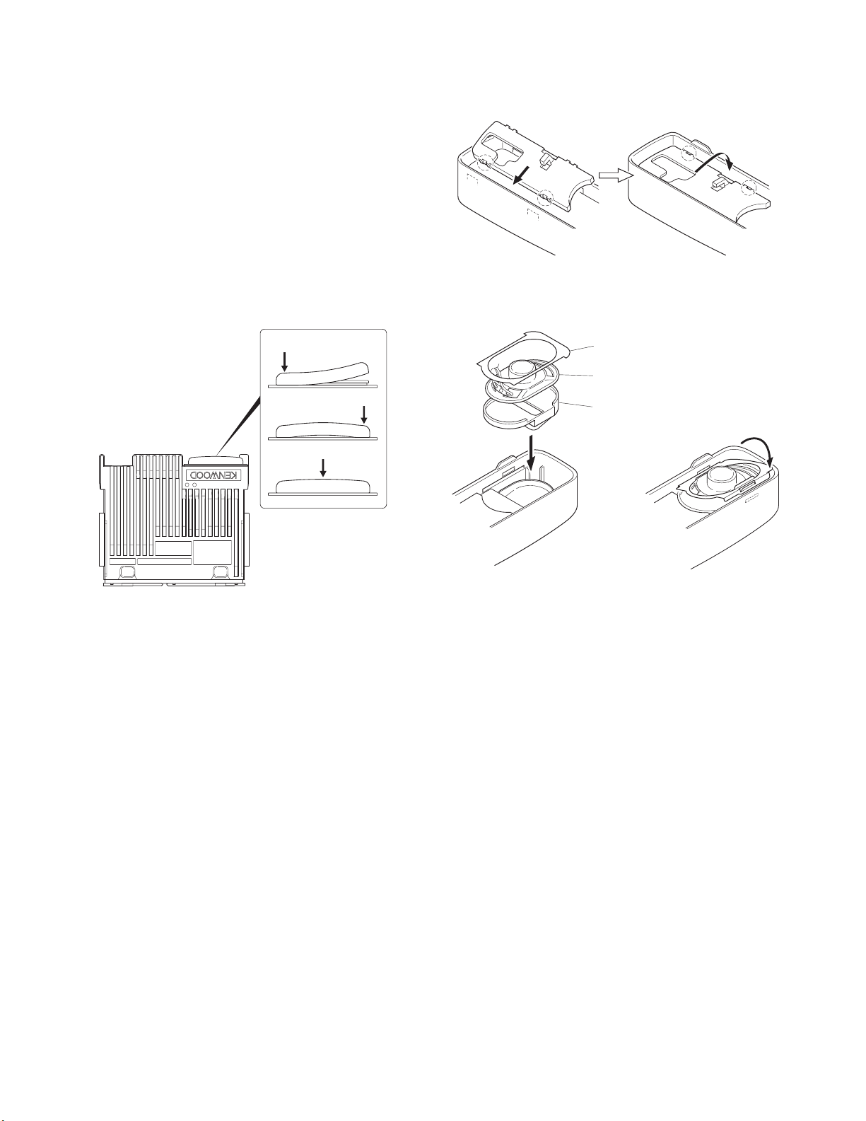
■ Top packing installation procedure
1. Place the top packing over the shielding plate.
2. Fit the convex tab of the top packing into the hollow of the
chassis. ( q )
3. Fit the chassis into the groove of the top packing. ( w )
Verify that the top packing is in close contact with the
chassis.
Fig. 5
17
TK-7180H/7182H
DISASSEMBLY FOR REPAIR
■ D-sub cap installation procedure
To improve water resistance, fit the D-sub cap into the Dsub terminal hardware fixture of the transceiver in the following order:
1. Fit the left side ( q ) of the D-sub cap into the hardware
fixture.
2. Fit the right side ( w ) of the D-sub cap into the hardware
fixture.
3. Fit the center ( e ) of the D-sub cap into the hardware fix-
ture.
Verify that the D-sub cap is in close contact with the hard-
ware fixture.
q
w
Fig. 7-1
q
w
e
Fig. 6
■ Installing the holder (J19-5485-02) and speaker
hardware fixture (J21-8481-03)
1. Insert two tabs of the holder (J19-5485-02) into the hol-
lows in the top of the panel. ( q )
2. Push the two tabs of the holder in on the opposite side of
those in step 1 above and fit them into the hollow in the
bottom of the panel. ( w )
Note : Push in the holder until it snaps in place.
3. Install the speaker holder onto the panel. ( e )
Note : To improve water resistance, fit the panel into the
groove of the holder.
4. Place the speaker into the speaker holder.
Note : The speaker must not ride on the holder rib.
5. Place the spacer on the speaker.
6. Insert the hardware fixture (J21-8481-03) into the hollow
of the panel as shown in Figure 7-3, then push two parts
of the hardware fixture and fit it into the hollow of the top
of the panel. (Fig. 7-3 r )
Note : Push in the hardware fixture until it snaps in place.
7. Insert the speaker connector into the display unit connec-
tor (CN901).
8. Place the speaker lead on the holder hook.
Spacer
Speaker
Speaker holder
e
Fig. 7-2 Fig. 7-3
r
18
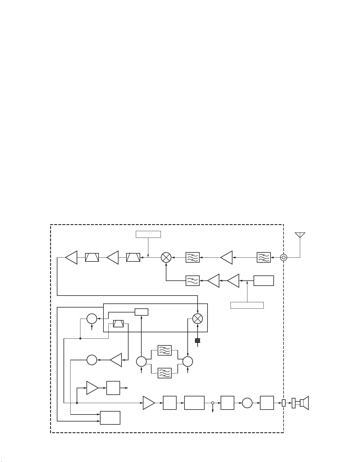
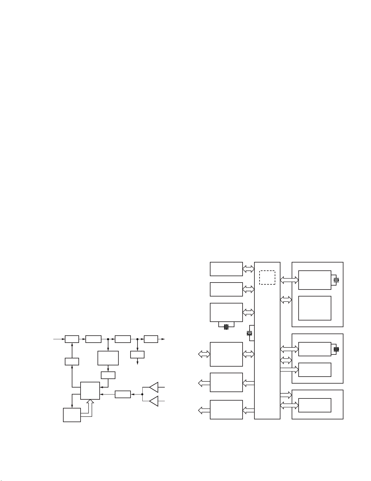
CIRCUIT DESCRIPTION
TK-7180H/7182H
1. Overview
This transceiver is a VHF/FM transceiver designed to oper-
ate in the frequency range of 136 to 174MHz.
The transceiver consists of receiver, transmitter, phase-
locked loop (PLL) frequency synthesizer, and control circuits.
2. Receiver Circuit
The receiver is double conversion superheterodyne, designed to operate in the frequency range of 136MHz to
174MHz.
The receiver circuit consists of the following circuits : 2-1
front-end circuit, 2-2 first mixer, 2-3 IF amplifier circuit, 2-4
audio amplifier circuit, and 2-5 squelch circuit.
2-1. Front-end Circuit
The front-end circuit consists of former BPF (D11), RF amplifier Q103, and latter BPF (D103, D104, D105 and D106).
The BPF covers frequency ranges 136 to 174MHz.
The latter BPF (D103, D104, D105 and D106) attenuates
the unwanted signals, and sends only the necessary signal to
the first mixer.
TX-RX UNIT (X57-698)
44.85MHz
IF AMP
Q172
MCF MCF
IF AMP
Q171
1st MIX DBM
IC171
2-2. First Mixer
The signal from the BPF is heterodyned with the first local
oscillator signal from the PLL frequency synthesizer circuit at
the first mixer DBM (IC171) to become a 44.85MHz first intermediate frequency (IF) signal. The first IF signal is fed
through a monolithic crystal filter (XF171) to further remove
spurious signals.
2-3. IF Amplifier Circuit
The first IF signal is amplified by Q171 and Q172, and then
enters IC172 (FM system IC). The signal is heterodyned
again with a second local oscillator signal (44.395MHz) with
in IC172 to become a 455kHz second IF signal. The second
IF signal is fed through a 455kHz ceramic filters (CF172;
Wide, CF171; Narrow) to further eliminate unwanted signal,
and the quadrature detection circuit FM-detects the signal to
produce a base-band signal and output it from pin 9.
2-4. Audio Amplifier Circuit
The demodulated audio signal from IC172 goes to IC415
through the AF amplifier (IC412) and IC413. The audio signal
goes to an electronic volume (IC410) and is amplified to drive
a loudspeaker by an audio power amplifier (IC417). The audio
output can be provided to external 4Ω speaker through the
speaker jack output (J401) on the rear panel. Q419 is a mute
switch.
136~174MHz
RX ANT
BPF
D103~D106
RF AMP
Q103
BPF
D11
RSSI
DET
SQL
XF171
(2/2)
Q178
SW
W/N
NOISE DET
D173
DET
IC407
ASQ
RSSI
XF171
(1/2)
FM SYSTEM IC : IC172
QUD
NOISE
AMP
Q175
SW
D172
IC410
DAC
IC404
CPU
CFSW
DEO
AMP
IC412 (B/2)
CF172
(Wide)
CF171
(Narrow)
455kHz
IC413
SW
LPF
SW
CFSW
IC415
AQUA
D171
-L
Buff AMP
Q313
X171
44.395MHz
AFO
Buff AMP
Q311
RX
+44.85MHz
f
180.85~218.85MHz
IC410
DAC
Q419
MUTE
Q306
RX VCO
IC417
AF
AMP
INT. SP
Fig. 1 Receiver circuit
19
TK-7180H/7182H
CIRCUIT DESCRIPTION
2-5. Squelch Circuit
The output signal from IC172 enters FM IC again, then
passed through a band-pass filter.
The noise component output from IC172 is amplified by
Q175 and rectified by D173 to produce a DC Voltage corresponding to the noise level. The DC voltage is sent to the
analog port of the CPU (IC404).
IC172 outputs a DC voltage (RSSI) corresponding to the
input of the IF amplifier.
3. Transmitter Circuit
The transmitter circuit consists of the following circuits : 31 microphone circuit, 3-2 modulation level adjustment circuit,
3-3 drive and final power amplifier circuit, and 3-4 automatic
power control circuit.
3-1. Microphone Circuit
The audio signal from the microphone goes into TX-RX
unit (X57-698) from the display unit (X54-348) and passes
through the mute switch (Q416). The audio signal is amplified by the microphone amplifier (IC414) and is input into the
TXIN terminal of the audio processor (IC415) after passing
through the multiplexer (IC413).
The input audio signal is output from the MOD terminal of
the audio processor (IC415) and is amplified by the audio frequency amplifier (IC412) after passing through the electric
volume (IC410).
DISPLAY UNIT
(X54-348) : TK-7180H
(X54-354) : TK-7182H
TX-RX UNIT (X57-698)
3-2. Modulation Level Adjustment Circuit
The audio signal amplified by the audio frequency amplifier (IC412) is added to the low speed data LSD passed
through the low pass filter (IC409). The combined signals is
supplied to the VCO (voltage controlled oscillator) and the
VCXO (voltage controlled crystal oscillator) X301, respectively.
3-3. Drive and Final Power Amplifier Circuit
The transmit signal obtained from the TX VCO buffer amplifier Q311, is amplified to approximately +17dBm by the
driver amplifiers Q313, Q1 and Q2. This amplified signal is
passed to the power amplifier module (power module) IC1,
which consists of a MOS-FET amplifier and is capable of
transmission output power.
3-4. Automatic Power Control Circuit
The automatic transmission power control (APC) circuit
stabilizes the transmitter output power at a predetermined
level by detecting the power module output with a diodes
D6, D7 and D8. Diodes D6, D7 and D8 apply a voltage to DC
amplifier IC72 (A/2). IC72 (B/2) compares the APC control
voltage (PC) generated by microprocessor IC404 and DC amplifier IC71 (A/2, B/2) with the detection output voltage from
IC72 (A/2) to control the Vgg pin of IC1, and stabilizes transmission output.
The APC circuit is configured to protect over-current of the
power module due to fluctuations of the load at the antenna
end and to stabilize transmission output at voltage and temperature variations.
J901
Modular
jack
MIC
SW
SW
D-SUB
MI2
IC414Q416
AMP
Q417
IC413
Multi-
plexer
TXIN
D-SUB
DI
LSDO
AQUA-L
IC409
LPF
MOD
IC410 IC412IC415
DAC
AMP
IC408
DC
AMP
Fig. 2 Microphone and modulation level adjustment circuit
Buff
Q313
Drive
AMP
Q1
Drive
AMP
PC
MP
Q2
Drive
AMP
DC
AMP
IC71 IC72
IC1
Final
AMP
DC
AMP
Gate
bias
D2~D4
SW
D6 D7
DET
DET
D8
DET
MOD
MB
Q307
TX VCO
VCXO
16.8MHz
X301
Q311
AMP
Fig. 3 Drive and Final power amplifier and automatic power control circuit
MOD
(for VCO)
MB
(for VCXO)
ANT
20
CIRCUIT DESCRIPTION
TK-7180H/7182H
4. PLL Frequency Synthesizer
The frequency synthesizer consists of the TCXO (X301),
VCO, PLL IC (IC301) and buffer amplifiers.
The TCXO generates 16.8MHz. The frequency stability is
2.5ppm within the temperature range of –30 to +60°C. The
frequency tuning and modulation of the TCXO are done to
apply a voltage to pin 1 of the TCXO. The output of the TCXO
is applied to pin 8 of the PLL IC.
The VCO consists of 2VCO and covers a dual range of
180.85~218.85MHz and 136~174MHz. The VCO generates
180.85~218.85MHz for providing to the first local signal in
receive. The operating frequency is generated by Q307 in
transmit mode and Q306 in receive mode. The oscillator frequency is controlled by applying the VCO control voltage, obtained from the phase comparator (IC301) to the variable capacitor diodes (D306, D308, D310 and D311 in transmit
mode and D307, D309, D312 and D313 in receive mode).
The T/R pin of IC404 goes “high” in receive mode causing
Q307 and Q309 to turn off, and Q306, Q308 and Q310 turn
on. The T/R pin goes “low” in transmit mode.
The outputs from Q306 and Q307 are amplified by buffer
amplifier (Q311) and doubled by Q301 and then sent to PLL
IC.
The PLL IC consists of a prescaler, reference divider,
phase comparator, charge pump (The frequency step of the
PLL circuit is 10, 12.5 or 15kHz). The input signal from the
pins 8 and 5 of the PLL IC is divided down to the 10, 12.5 or
15kHz and compared at phase comparator. The phase comparator output signal is fed into a low-pass filter (Q302, Q303
and Q304) before being applied to the VCO as a frequency
control voltage. This low-pass filter’s power is supplied by
the DC/DC converter (IC251 and Q251). The DC signal is applied to the CV of the VCO and locked to keep the VCO frequency constant.
PLL data is output from DT (pin 112), PCK (pin 82) and PLE
(pin 81) of the microprocessor (IC404). The data are input to
the PLL IC when the channel is changed or when transmission is changed to reception and vice versa. A PLL lock condition is always monitored by the pin 80 (UL) of the microprocessor. When the PLL is unlocked, the UL goes low.
5. Control Circuit
The block diagram of the control circuit is shown in Fig-
ure 5.
The CPU (IC404) is a 16-bit microcomputer that contains a
256k-byte Mask ROM and a 20k-byte RAM. This CPU is connected with an external 512k-byte Flash ROM (IC405) and
operates in memory expansion mode.
The Firmware Program is stored in the Flash ROM and the
user data and adjustment data are stored in the EEPROM
(IC401). The CPU and Flash ROM are connected with an 8 bit
bus and the EEPROM and RTC IC : IC402 (TK-7180H only) are
connected with a I2C bus (*1). The RTC IC (TK-7180H only)
has a clock function and is controlled by the CPU (IC404).
Serial communication with a PC is performed through two
paths: through the 232C Level converter IC (IC416) and
through the Display Unit Panel CPU (IC902). The 8 bit Shift
Register (IC403) is used as an 8-port Extended Output Port.
IC410 is an 8 bit-8ch D/A converter. The channels are set as
follows:
Ch1 : Modulation balance
Ch2 : Deviation Factor
Ch3 : Max Power Level
Ch4 : Reception tuning circuit
Ch5 : Deviation Factor
Ch6 : Speaker volume
Ch7 : VCXO control voltage
Ch8 : DEO output level
*1: I2C bus is a registered trademark of PHILIPS of the Netherlands.
IC405
Flash ROM
IC401
EEPROM
IC402
RTC IC
(TK-7180H only)
Mask
ROM
Display unit
IC902
CPU
(TK-7180H only)
IC903 (TK-7180H)
IC902 (TK-7182H)
LCD
driver
T/R
T/R
(TX : Low)
Q302~
Q304
Q311
BUFF
CV
LPF
IC301
20
PLL
15
UL
CPU
DT,PCK,PLE
IC404
Q301
Doubler
x2
BPF
5
8
Q313
BUFFVCO
To mixer
TCXO
X301
Fig. 4 PLL block diagram
SW
MB
D316
SW
D315
IC408
To
drive
AMP
FC
BAL
Signal block
IC415
AQUA-L
IC413
Multiplexer
RF block
IC301
PLL IC
IC416
232C
Level
converter
IC403
8bit Shift
register
IC410
D/A
converter
IC404
CPU
Fig. 5 Control circuit block diagram
21
TK-7180H/7182H
CIRCUIT DESCRIPTION
6. Power Supply Circuit
The block diagram of the power supply circuit is shown in
Figure 6.
Power is always supplied from +B to the circuit (5M, +B)
that is always started and the circuits (SB, 8C, 5E, 8T, 8R, 5C,
5R) controlled by the CPU (IC404). When +B is supplied to
the transceiver, Q801, D805 and IC805, regulate the voltage
(5M) which is supplied to the circuit around the CPU. The
CPU starts.
When the CPU detects that the +B voltage is higher than
the voltage prescribed by IC802, the transceiver power (SB)
is turned ON by controlling the SBC signal (Low: transceiver
power OFF, High: transceiver power ON).
The CPU controls the TXC signal (Low: Transmission system power OFF, High: Transmission system power ON) during transmission to supply power (8T) to the transmission circuit. The CPU controls the RXC signal (Low: Reception system power OFF, High: Reception system power ON) during
reception to supply power (8R, 5R) to the reception circuit.
When the CPU detects the PSW (Power Switch) signal,
IGN (Ignition Sense) signal or INT signal, it controls the SBC
signal and turns the transceiver power (SB) OFF.
If +B is not provided to the transceiver, power is supplied
to only the RTC IC (IC402) through the secondary battery connected with CN401 to back up the clock.
Power supply : 10.8~15.7V
F801
5A
D804
DET
Q801,D805
REG
IC802
DET
Q802
SW
Q811
SW
IC805
AVR
IC801
DET
Q810
SW
Q807
SW
5M
CN401
IC803
AVR
SBC
CPU
Flash memory
EEPROM
Ext-I/O
CPU #17
: RST1
RTC IC
TK-7180H
only
IC807
AVR
Q803
SW
Q806
SW
Q804
SW
Q808
SW
IC804
AVR
Q805
SW
+B
Final AMP
SB
Audio AMP, PA connector
Panel block, D-sub block
8C
Internal option
Panel block
5E
Internal option
TX-drive
8T
APC block
ANT SW
TXC
8R
IF block
RXC
VCXO, VCO, PLL IC
IF detection IC
5C
DC/DC converter
D/A converter
MIC AMP, AQUA-L
AF block
5R
IF block
22
CPU #24
: INT
Q809
SW
Fig. 6 Power supply circuit
RXC
CIRCUIT DESCRIPTION
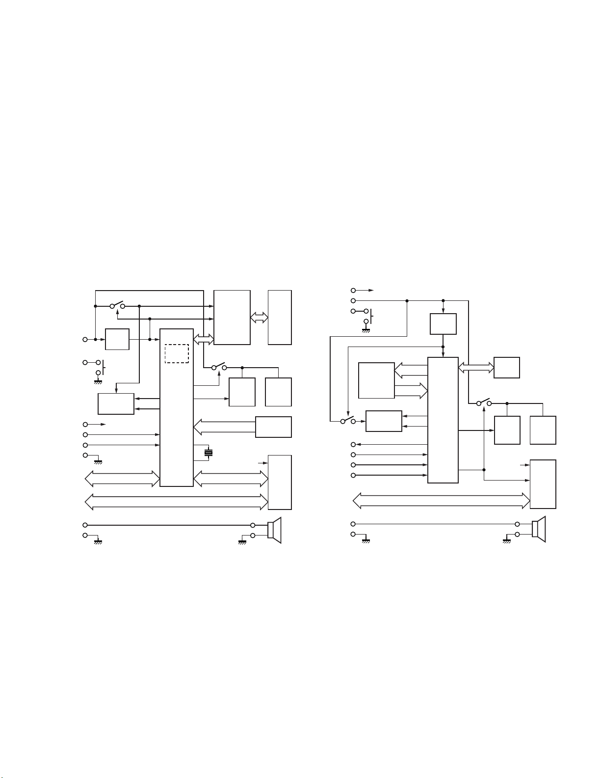
7. Display Circuit
7-1. TK-7180H Transceiver
The display unit consists of the Panel CPU (IC902), the
LCD driver (IC903), the TX/BUSY LED, the KEY detection, the
Backlight and the Microphone jack circuits.
The Panel CPU is a 16-bit microcomputer that contains a
64k-byte Mask ROM and a 2k-byte RAM.
The Panel CPU performs serial communication with the
Main CPU (IC404) on the TX-RX unit (B/3) and the Panel CPU
detects keys and sends data communication contents
through the MIC Jack to the Main CPU. The Panel CPU receives commands from the Main CPU and controls the display system.
The LCD operates with 1/9 duty under the LCD driver
(IC903) control. The LCD and KEY Backlights are controlled
by Q909. The display brightness of the LCD Backlight can be
changed.
TK-7180H/7182H
7-2. TK-7182H Transceiver
The display unit consists of the LCD driver (IC902), the TX/
BUSY LED, the KEY detection, the Backlight and the Microphone jack circuits.
The LCD driver performs serial communication with the
Main CPU (IC404) on the TX-RX unit (B/3) and the LCD driver
detects keys and sends data to the Main CPU. The LCD
driver receives commands from the Main CPU and controls
the display system.
The LCD operates with 1/4 duty under the LCD driver
(IC902) control. The LCD and KEY Backlights are controlled
by Q908. The display brightness of the LCD Backlight can be
changed by Q909.
8C
PSW
SB
RST2
SHIFT
PSENS
SPO
GND
Q910
IC903
LCD
IC901
AVR
POWER
SW
TX/Busy
LED
RXD, TXD
RED
GRN
Mask
ROM
IC902
CPU
MIC, ME
driver
Q909
BLC1
DIMM
HK, PTT, DM, BLC2
LCD
back
light
FKEY [1~10]
Fig. 7 TK-7180H Display circuit
SB
LCD
KEY
back
light
Function
KEY
MIC
jack
SP
SB
8C
PSW
Q902
LCDDO
LCDCS
LCDCLK
LCDDI
SPO
GND
POWER
Function
KEY
TX/Busy
LED
SW
KS [5,6]
KI [1~5]
PTT, ME, MIC, HOOK, DM
RED
GRN
IC901
AVR
IC902
LDC
driver
Q908
DIMM
BLC
Fig. 8 TK-7182H Display circuit
LCD
LCD
back
light
KEY
back
light
SB
J901
MIC
jack
SP
23

TK-7180H/7182H
SEMICONDUCTOR DATA
Microprocessor : 30625MGP169GU (TX-RX unit IC404) : TK-7180H
Pin No. Port Name I/O Function
1VREF-+5V
2 AVCC - +5V
3 SBC O Switched B control
4 RXC O RX control
5 TXC O TX control
6PCOTX APC adjust
7 HSDO O High speed data output
8 STSW O Side tone switch
9 RTCL/EEPCL O RTC/EEPROM clock
10 HSDIN I High speed data input
11 NC - No connection
12 RTDT/EEPDAT I/O RTC/EEPROM data
13 BYTE - +5V
14 CNVSS - DGND (Vss)
15 DMUTE O Det mute
16 AM2 O Audio mute 2
17 RST I Reset
18 Xout O 11.0592MHz clock output
19 DGND - DGND (Vss)
20 Xin I 11.0592MHz clock input
21 VCC1 - +5V
22 NMI - +5V
23 PSW I Power switch input
24 INT I BATT voltage INT
25 INTRA I RTC INT
26 SHIFT/MODEL I/O Beat shift/Model select
27 BEEP O Beep output
28 SPSTB O Shift register strobe
29 SOE O Shift register output enable
30 AIO5 I/O AUX I/O 5
31 AIO9 I/O AUX I/O 9
32 DSTB O D/A converter LD
33 LSDO O Low speed data output
34 RXD2 I RXD2
35 TXD2 O TXD2
36 TXD1 O TXD1/PTT (Scrambler board)
37 Vcc1 - +5V
38 RXD1 I RXD1
39 DGND - DGND (Vss)
40 MM1 O MIC mute 1
41 PSENS I Panel sense
42 TXD O TXD
43 RXD I RXD
44 AFDAT O BB TDATA and DTRCLK
45 AFDIO I/O BB DI/O
46 AFDIR O BB DIR
47 DTRLOAD O BB DTMF enable
48 AFSTD I BB STD
24
Pin No. Port Name I/O Function
49 LSW O BB LIM switch
50 RDY - +5V
51 NC - No connection
52 HOLD - +5V
53 NC - No connection
54~57 AIO4~AIO1 I/O AUX I/O 4~1
58 NC - No connection
59 RD O Read (RD)
60 NC - No connection
61 WR O Write (WR)
62~64 AIO8~AIO6 I/O AUX I/O 8~6
65,66 NC - No connection
67 RST2 O Display µ-com reset
68 CS0 O Chip select 0
69 NC - No connection
70~79 A18~A9 O Address bus 18~9
80 UL I PLL unlock
81 PLE O PLL enable
82 PCK O PLL clock
83 NC - No connection
84 OPT6 I/O Option board I/F 6
85 VCC2 - +5V
86 A8 O Address bus 8
87 DGND - DGND (Vss)
88~95 A7~A0 O Address bus 7~0
96 IGN I Ignition sense
97 AFRTM I BB RDF/FD
98 TCLK/DTRDO I BB TCLK and DTRDO
99 MM2 O MIC mute 2
100 T/R O TX/RX switch
101 AM1 O Audio mute 1
102 EMTON O EM tone switch
103 NC - No connection
104~111 D7~D0 I/O Data bus7~0
112 DT O Serial data
113 CK O Serial clock
114 W/N O Wide/Narrow switch
115~117 OPT 1~OPT 3 I/O Option board I/F 1~3
118,119 OPT 4, OPT 5 O Option board I/F 4, 5
120 H/L O High/Low power switch
121 THP I TX thermal input
122,123 NC - No connection
124 ASQ I RX analog squelch input
125 RSSI I RX RSSI input
126 NC - No connection
127 AGND - AGND (Vss)
128 LSDIN I Low speed data input
TK-7180H/7182H
SEMICONDUCTOR DATA
Microprocessor : 30625MGP238GU (TX-RX unit IC404) : TK-7182H
Pin No. Port Name I/O Function
1VREF-+5V
2 AVCC - +5V
3 SBC O Switched B control
4 RXC O RX control
5 TXC O TX control
6PCOTX APC adjust
7 HSDO O High speed data output
8 STSW O Side tone switch
9 EEPCL O EEPROM clock
10 HSDIN I High speed data input
11 DM I DTMF MIC key scan
12 EEPDAT I/O EEPROM data
13 BYTE - +5V
14 CNVSS - DGND (Vss)
15 DMUTE O Det mute
16 AM2 O Audio mute 2
17 RST I Reset
18 Xout O 11.0592MHz clock output
19 DGND - DGND (Vss)
20 Xin I 11.0592MHz clock input
21 VCC1 - +5V
22 NMI - +5V
23 PSW I Power switch input
24 INT I BATT voltage INT
25 INTRA - +5V
26 SHIFT/MODEL I/O Beat shift/Model select
27 BEEP O Beep output
28 SPSTB O Shift register strobe
29 SOE O Shift register output enable
30 AIO5 I/O AUX I/O 5
31 AIO9 I/O AUX I/O 9
32 DSTB O D/A converter LD
33 LSDO O Low speed data output
34 RXD2 I RXD2
35 TXD2 O TXD2
36 TXD1 O TXD1/PTT (Scrambler board)
37 Vcc1 - +5V
38 RXD1 I RXD1
39 DGND - DGND (Vss)
40 MM1 O MIC mute 1
41 PTT I PTT input
42 TXD O TXD
43 RXD/HOOK I RXD/HOOK
44 AFDAT O BB TDATA and DTRCLK
45 AFDIO I/O BB DI/O
46 AFDIR O BB DIR
47 DTRLOAD O BB DTMF enable
48 AFSTD I BB STD
Pin No. Port Name I/O Function
49 LSW O BB LIM switch
50 RDY - +5V
51 NC - No connection
52 HOLD - +5V
53 NC - No connection
54~57 AIO4~AIO1 I/O AUX I/O 4~1
58 NC - No connection
59 RD O Read (RD)
60 NC - No connection
61 WR O Write (WR)
62~64 AIO8~AIO6 I/O AUX I/O 8~6
65 LCDDO O LCD serial data output
66 LCDCLK I LCD serial clock
67 LCDCS I LCD chip select
68 CS0 O Chip select 0
69 NC - No connection
70~79 A18~A9 O Address bus 18~9
80 UL I PLL unlock
81 PLE O PLL enable
82 PCK O PLL clock
83 NC - No connection
84 OPT6 I/O Option board I/F 6
85 VCC2 - +5V
86 A8 O Address bus 8
87 DGND - DGND (Vss)
88~95 A7~A0 O Address bus 7~0
96 IGN I Ignition sense
97 AFRTM I BB RDF/FD
98 TCLK/DTRDO I BB TCLK and DTRDO
99 MM2 O MIC mute 2
100 T/R O TX/RX switch
101 AM1 O Audio mute 1
102 EMTON O EM tone switch
103 LCDDI I LCD serial data input
104~111 D7~D0 I/O Data bus 7~0
112 DT O Serial data
113 CK O Serial clock
114 W/N O Wide/Narrow switch
115~117 OPT 1~OPT 3 I/O Option board I/F 1~3
118,119 OPT 4, OPT 5 O Option board I/F 4, 5
120 H/L O High/Low power switch
121 THP I TX thermal input
122,123 NC - No connection
124 ASQ I RX analog squelch input
125 RSSI I RX RSSI input
126 NC - No connection
127 AGND - AGND (Vss)
128 LSDIN I Low speed data input
25
TK-7180H/7182H
SEMICONDUCTOR DATA
Microprocessor : 30302M88Z7GU (Display unit IC902) : TK-7180H only
Pin No. Port Name I/O Function
1~4 NC - No connection
5 SHIFT O Beat shift
6BYTE-+5V
7 CNVSS - GND
8,9 NC - No connection
10 RST I Reset
11 Xout O 14.7456MHz clock output
12 GND - GND
13 Xin I 14.7456MHz clock input
14 VCC - +5V
15 NMI - +5V
16 BLC2 O MIC backlight control
17 BLC1 O Key & LCD backlight control
18 DIMM O Dimmer control
19 LEDG O LED green
20 LEDR O LED red
21 NC - No connection
22 LCDCK O LCD serial clock
23 LCDDT O LCD serial data
24 LCDCS O LCD chip select
25 LCDRST O LCD reset
26 NC - No connection
27 RXD2 I RXD2 (Main µ-com)
28 TXD2 O TXD2 (Main µ-com)
29 PTT/TXD I/O PTT/TXD (COM0)
30 NC - No connection
31 DM O MIC DM
32,33 NC - No connection
34 HK/RXD I HOOK/RXD (COM0)
35~59 NC - No connection
60 VCC - +5V
61 NC - No connection
62 VSS - GND
63~70 NC - No connection
71~82 S22~S11 I No connection
83 S10 I Front panel key (R down [ ])
84 S9 I Front panel key (R up [ ])
Pin No. Port Name I/O Function
85 S8 I Front panel key (■ )
86 S7 I Front panel key (C)
87 S6 I Front panel key (B)
88 S5 I Front panel key (A)
89 S4 I Front panel key (S)
90 S3 I Front panel key ( )
91 S2 I Front panel key (L down [ ])
92 S1 I Front panel key (L up [ ])
93 NC - No connection
94 AVSS - GND
95 NC - No connection
96 VREF - +5V
97 AVCC - +5V
98~100 NC - No connection
Shift Register : BU4094BCFV (TX-RX unit IC403)
Pin No. Port Name I/O Function
1 STRB I Storage enable input
2 DATA I Serial data input
3 CLK I Serial clock input
4Q1OAUX output 1
5Q2OPublic address
6Q3OHorn alert
7Q4OScrambler switch
8 Vss -
9Qs O
10 Q’s O
11 Q8 O Ceramic filter switch
12 Q7 O No connection
13 Q6 O AUX output 2
14 Q5 O Gate switch
15 OE I Output enable
16 VDD -
26
TK-7180H/7182H
COMPONENTS DESCRIPTION
Display unit (X54-3480-10) : TK-7180H
Ref. No. Part Name Description
IC901 IC Voltage regulator/ 5V
IC902 IC Microprocessor
IC903 IC LCD driver
Q901,902 Transistor Hook switch
Q904 Transistor TX indication LED switch
Q905 Transistor Busy indication LED switch
Q906 Transistor Dimmer switch control
Q907 Transistor Dimmer switch
Q909 Transistor Backlight control switch
Q910 Transistor 8C switch
Q911 Transistor 8C switch control
Q913 Transistor Backlight control
D901,902 Zener diode Voltage protection
D903 Varistor Current limiter
D904~906
D907 LED TX/Busy indication
D909~920
D921~930
Diode Surge protection
LED LCD backlight
LED KEY backlight
Display unit (X54-3540-10) : TK-7182H
Ref. No. Part Name Description
IC901 IC Voltage regulator/ 5V
IC902 IC LCD driver
Q901,903 Transistor Hook switch
Q902 Transistor 8C switch
Q904 Transistor 8C switch control
Q905 Transistor TX indication LED switch
Q906 Transistor Busy indication LED switch
Q907 Transistor Backlight switch control
Q908 Transistor Backlight switch
Q909 Transistor Dimmer switch
D902 Zener diode Voltage protection
D903 Varistor Current limiter
D904 Diode Isolator
D906 Diode Surge protection
D908 LED TX/Busy indication
D909~920
D921~930
D931~933
LED LCD backlight
LED KEY backlight
Varistor Surge protection
TX-RX unit (X57-6980-XX)
Ref. No. Part Name Description
IC1 IC Power module
IC71,72 IC DC amp for TX APC
IC171 IC RX 1st mixer
IC172 IC FM IF system IC
IC251 IC DC-DC converter
IC301 IC PLL system IC
IC302 IC PLL CP switch
IC401 IC EEPROM
IC402 IC RTC processor
IC403 IC Shift register
IC404 IC Microprocessor
IC405 IC Flash memory
IC406 IC HSD BPF/HSD comparator
IC407 IC DET amp/Data LPF (DB-25)
IC408 IC LSD buffer amp/VCXO bias amp
IC409 IC LSD LPF/Voltage DC-reference
IC410 IC D/A converter
IC411 IC RF BPF tuning voltage DC amp
IC412 IC Modulation LPF/DET amp
IC413 IC AF switch IC
IC414 IC MIC amp
IC415 IC AQUA-L
IC416 IC Level converter IC (RS-232C)
IC417 IC Audio IC
IC801 IC Voltage detector (CPU reset)
IC802 IC Voltage detector (INT)
IC803 IC Voltage regulator/ 8V
IC804,805
IC807 IC Voltage regulator/ 5V
Q1 Transistor TX pre-driver
Q2 Transistor TX driver
Q3 Transistor TX gate switch
Q72 FET High/Low power switch
Q73 Transistor High/Low power switch
Q103 Transistor Front-end LNA
Q171,172 Transistor IF amp
Q173,174 Transistor W/N CF switch control
Q175 Transistor Noise amp
Q176 FET DET mute switch
IC Voltage regulator/ 5V
27
TK-7180H/7182H
COMPONENTS DESCRIPTION
Ref. No. Part Name Description
Q177 Transistor W/N CF switch control
Q178 Transistor W/N discrete switch
Q180 Transistor W/N CF switch control
Q251 Transistor Ripple filter
Q301 Transistor PLL f-in doubler amp
Q302~304
Q305 Transistor PLL f-in filter switch control
Q306,307 FET TX/RX VCO
Q308~310
Q311 Transistor VCO buffer amp
Q312 Transistor Ripple filter
Q313 Transistor VCO buffer amp
Q314 Transistor PLL f-in filter switch control
Q402 Transistor Beat shift switch
Q405 Transistor AQUA control switch
Q406 FET AF switch (LSD)
Q409 Transistor AF mute switch
Q410,411 Transistor MIC AGC
Q412 FET AF mute switch
Q413,414 FET AF switch
Q415 FET AF switch (Voice)
Q416,417 FET MIC mute switch
Q418 Transistor AF mute control switch
Q419 Transistor AF mute switch
Q421 Transistor MIC mute switch
Q701,702 Transistor Inverter switch
Q801 Transistor Voltage regulator/ 8.5V
Q802 Transistor SB control switch
Q803 Transistor 8T switch
Q804 Transistor 8R switch
Q805 Transistor 5R switch
Q806 Transistor 8T control switch
Q807 Transistor SB control switch
Q808 Transistor 8R control switch
Q809 Transistor 5R control switch
Q810 FET SB switch
Q811 Transistor CPU reset switch
Transistor PLL LPF
Transistor TX/RX VCO switch
Ref. No. Part Name Description
Q812 Transistor Ignition sense control switch
D1 Zener diode Voltage protection
D2~4 Diode ANT switch
D6~8 Diode RF detector
D11 Variable RF BPF tuning
capacitance diode
D103~106
D171,172 Diode W/N CF switch
D173 Diode SQ noise amp detector
D174 Diode DET mute switch control
D251 Diode Reverse voltage protection
D301,302 Diode PLL f-in filter switch
D304,305 Diode PLL f-in filter switch
D306~313
D314 Variable Modulation control for TX VCO
D315,316 Diode TX/RX band switch
D402~404
D405,406 Zener diode Voltage protection
D407 Diode DC detector
D408,409 Diode MIC amp AGC detector
D412~414
D416 Diode AF mute control
D417,418 Diode Isolator
D419,420 Diode MIC mute control
D421~423
D701 Zener diode Voltage protection
D702,703 Diode Voltage protection
D704~708
D709,710 Zener diode Voltage protection
D711~713
D714 Zener diode Voltage protection
D801 Surge absorber Voltage protection
D802 Diode DC reverse connection protect
D804,805 Zener diode Voltage protection
Variable RF BPF tuning
capacitance diode
Variable
capacitance diode
capacitance diode
Diode RTC battery control
Diode Surge protect
Diode Voltage protection
Diode Surge protect
Diode Surge protect
Frequency control for TX/RX VCO
28
PARTS LIST
CAPACITORS
C C 4 5 T H 1 H 2 2 0 J
1234 56
1 = Type ... ceramic, electrolytic, etc. 4 = Voltage rating
2 = Shape ... round, square, etc. 5 = Value
3 = Temp. coefficient 6 = Tolerance
• Temperature coefficient
1st Word C L P R S T U
Color* Black Red Orange Yellow Green Blue Violet
ppm/°C0 –80 –150 –220 –330 –470 –750
TK-7180H/7182H
CC45
Color*
2nd Word G H J K L
ppm/°C ±30 ±60 ±120 ±250 ±500
Example : CC45TH = –470±60ppm/°C
• Capacitor value
010 = 1pF 2 2 0 = 22pF
100 = 10pF
101 = 100pF Multiplier
102 = 1000pF = 0.001µF 2nd number
103 = 0.01µF 1st number
• Tolerance (More than 10pF)
Code C D G J K M X Z P No code
(%) ±0.25 ±0.5 ±2 ±5 ±10 ±20 +40 +80 +100 More than 10µF : –10~+50
–20 –20 –0 Less than 4.7µF : –10~+75
• Voltage rating
2nd word
1st word
0 1.0 1.25 1.6 2.0 2.5 3.15 4.0 5.0 6.3 8.0 –
11012.5 16 20 25 31.5 40 50 63 80 35
2 100 125 160 200 250 315 400 500 630 800 –
3 1000 1250 1600 2000 2500 2150 4000 5000 6300 8000 –
ABCDEFGHJKV
CHIP CAPACITORS
(EX) C C 7 3 F S L 1 H 0 0 0 J Refer to the table above.
12345 67 1 = Type
(Chip) (CH, RH, UJ, SL) 2 = Shape
3 = Dimension
(EX) C K 7 3 F F 1 H 0 0 0 Z 4 = Temp. coefficient
12345 67 5 = Voltage rating
(Chip) (B, F) 6 = Value
7 = Tolerance
RESISTORS
• Chip resistor (Carbon)
(EX) R D 7 3 E B 2 B 0 0 0 J
12345 67
(Chip) (B, F)
• Carbon resistor (Normal type)
(EX) R D 1 4 B B 2 C 0 0 0 J
12345 67
(Chip) (B, F)
1 = Type ... ceramic, electrolytic, etc. 5 = Voltage rating
2 = Shape ... round, square, etc. 6 = Value
3 = Dimension 7 = Tolerance
4 = Temp. coefficient
(Less than 10pF)
Code B C D F G
(pF) ±0.1 ±0.25 ±0.5 ±1 ±2
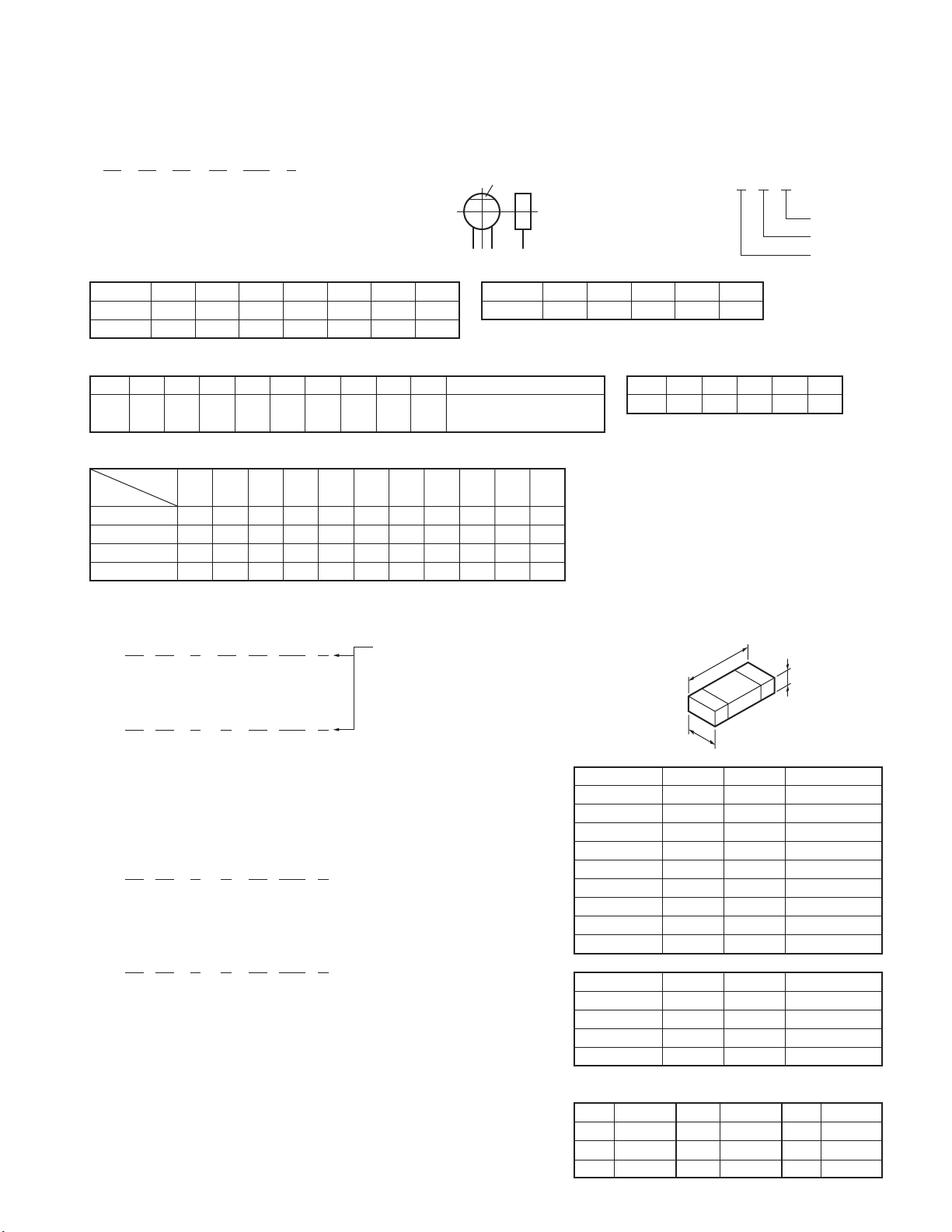
• Dimension
L
T
W
Chip capacitor
Code L W T
Empty 5.6±0.5 5.0±0.5 Less than 2.0
A 4.5±0.5 3.2±0.4 Less than 2.0
B 4.5±0.5 2.0±0.3 Less than 2.0
C 4.5±0.5 1.25±0.2 Less than 1.25
D 3.2±0.4 2.5±0.3 Less than 1.5
E 3.2±0.2 1.6±0.2 Less than 1.25
F 2.0±0.3 1.25±0.2 Less than 1.25
G 1.6±0.2 0.8±0.2 Less than 1.0
H 1.0±0.05 0.5±0.05 0.5±0.05
Chip resistor
Code L W T
E 3.2±0.2 1.6±0.2 1.0
F 2.0±0.3 1.25±0.2 1.0
G 1.6±0.2 0.8±0.2 0.5±0.1
H 1.0±0.05 0.5±0.05 0.35±0.05
• Rating wattage
Code Wattage Code Wattage Code Wattage
1J 1/16W 2C 1/6W 3A 1W
2A 1/10W 2E 1/4W 3D 2W
2B 1/8W 2H 1/2W
29
 Loading...