

Kenwood DM-3090 Service manual
STEREO MINIDISC RECORDER
MULTI CONTROL
TIME DISPLAY
DISPLAY/CHARAC.
TRACK/EDIT
ON/STAND BY
STEREO MINIDISC RECORDER
TIMER/
DELETE
ENTER
REC REC LEVEL
0 10
PHONES LEVEL
MIN MAX
PHONES
R
L
R
L
PLAY
OUT
REC
IN
DIGITAL
LINE
2
REC IN
1
REC INPLAY OUT
OPT.
RESET
DM-3090
SERVICE MANUAL
© 1997-11/B51-5396-00 (K/K) 1812
KENWOOD badge
(B43-0302-04)
Knob (POWER)
(K27-2261-08)
AC power cord bushing
(J42-0338-08)
Front glass
(B10-2457-08)
Panel
(A29-0898-08)
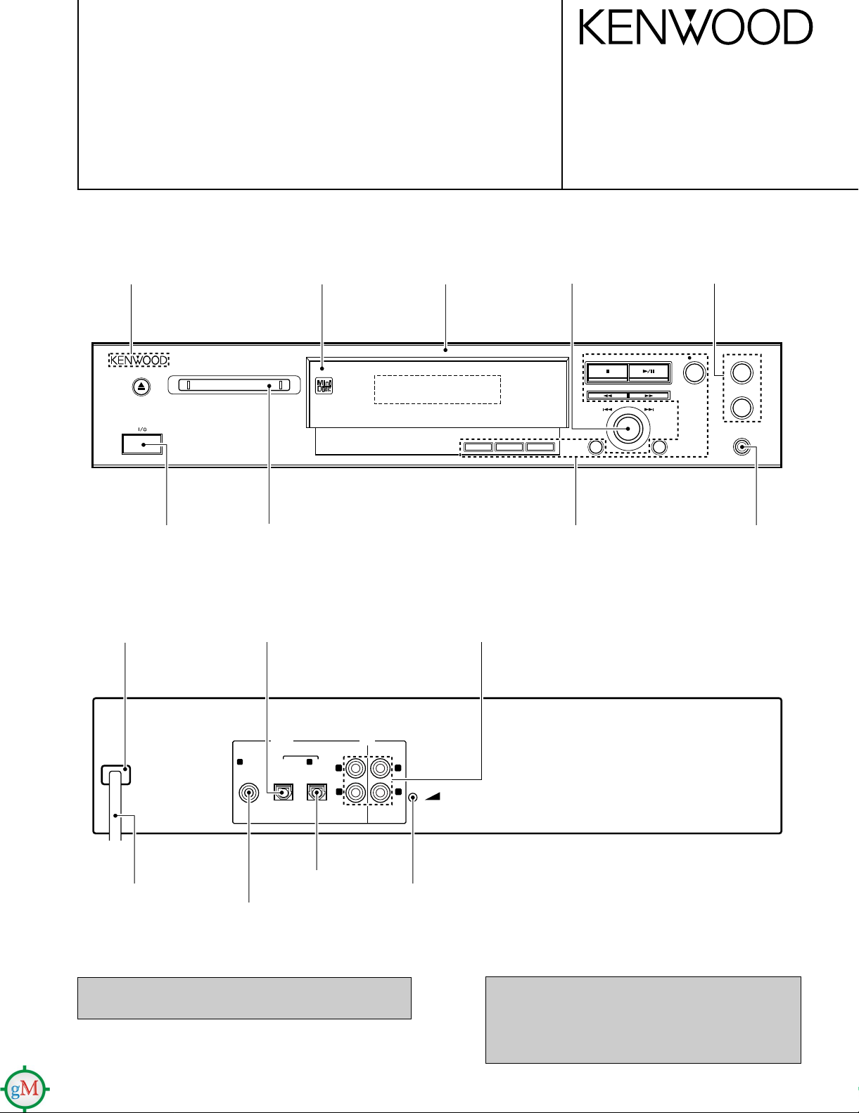
Optical digital input
(W02-2643-08)
Front panel
(A60-1370-08)
Analogue output terminal
(E63-1031-08)
Knob (JOG)
(K29-6946-08)
Knob
(K27-2262-08)
Knob (REC/HP)
(K29-6947-08)
Head phone jack
(E11-0345-08)
Optical digital output
AC power cord *
(E30-)
Digital input terminal
(E63-1032-08)
In compliance with Federal Regulations, following are
reproductions of labels on, or inside the product relating to
laser product safety,
(W02-2643-08)
Switch (RESET)
(S68-0091-08)
*Refer to parts list on page 49.
KENWOOD-Corp. certifies this equipment conforms to
DHHS Regulation No.21 CFR 1040.10, Chapter 1,
Subchapter J.
DANGER : Laser radiation when open and interlock
defeated.
AVOID DIRECT EXPOSURE TO BEAM.
If a problem occurs
If this product is subjected to strong external interference
(mechanical shock, excessive static electricity, abnormal
supply voltage due to lightning, etc.) or if it is operated
incorrectly, it may malfunction or the display may not
function correctly. If such a problem occurs, do the
following:
• Unplug the AC power lead from the AC socket.
• Wait about 20 - 30 seconds and then plug the AC power
lead back into the AC socket.
• Press the reset key on the back of the unit.
• When the reset key is pressed, all of the settings in memory
will be erased.
Beware of condensation
When water vapor comes into contact with the surface of
cold material, water drops are produced. If condensation
occurs, correct operation may not be possible, or the unit
may not function correctly.
This is not a malfunction, however, and the unit should be
dried.
(To do this, turn the POWER switch ON and leave the unit
as it is for several hours.)
Be especially careful in the following conditions:
• When the unit is brought from a cold place to a warm place
and there is a large temperature difference.
• When a heater starts operating.
• When the unit is brought from an air-conditioned place to
a place of high temperature with high humidity.
• When there is a large difference between the internal
temperature of the unit and the ambient temperature, or in
conditions where condensation occurs easily.
619
+10
2 3
4 5
7 8
0
DM-3090
CONTENTS/ACCESSORIES/CAUTIONS
CONTENTS
CONTENTS/ACCESSORIES/CAUTIONS...................2
CONTROLS.................................................................3
DISASSEMBLY FOR REPAIR.....................................5
BLOCK DIAGRAM.......................................................7
CIRCUIT DESCRIPTION.............................................9
TROUBLE SHOOTING..............................................16
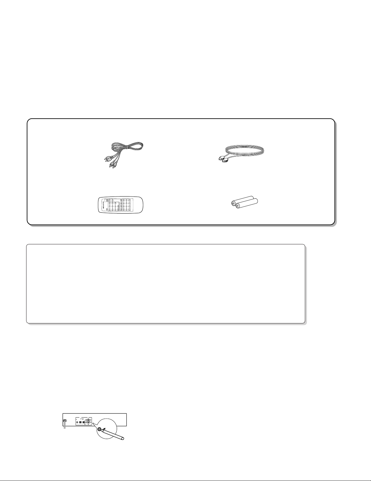
Accessories
ADJUSTMENT...........................................................24
PC BOARD ............................................................... 32
SCHEMATIC DIAGRAM........................................... 37
EXPLODED VIEW .....................................................47
PARTS LIST...............................................................49
SPECIFICATIONS .......................................Back cover
Audio cord (2)
(E30-0505-05)
Remote control unit (1)
(A70-1208-08)
Battery cover (A09-0337-08)
Cautions
Optical fiber cable (1)
(B19-1529-05)
Batteries (2)
2
DIGITAL
LINE
REC
PLAY
OPT.
IN
OUT
2
REC IN1REC INPLAY OUT
L
RLR
RESET
RESET

Names and functions of parts
MULTI CONTROL
TIME DISPLAY
DISPLAY/CHARAC.
TRACK/EDIT
ON/STAND BY
STEREO MINIDISC RECORDER
TIMER/
DELETE
ENTER
REC REC LEVEL
0 10
PHONES LEVEL
MIN MAX
PHONES
1
2
3
456789
0!
@
#
$
%
^
1 Eject key:
2 Power switch (ON/STAND BY key)
3 Mini Disc Insertion slot
4 TIME DISPLAY key
5 DISPLAY/CHARAC key
6 TRACK/EDIT key
7 TIMER/DELETE key
8 Jog dial (Next/Previous)
9 ENTER key
0 Headphone jack (HONES)
! Headphone output level control
@ Record level control
# Record key:
$ Play/Pause key:
% Stop key:
^ Cue/Review key: /
−
∞
TOC DISC
TOTAL
REMAIN
RANDOM
TIMER REC CLOCK
TRACK
DATE 0dB OVER12 4
MONO LP PRGM
1
8
15
2
9
16
3
10
17
4
11
18
5
12
19
6
13
20
7
14
1
2
3
456
7
8
9
0
!
@
#
$
%
^
&
*
(
1 Pause indicator:
2 Record indicator:
3 Play indicator:
4 Monaural Long-Play Mode indicator
5 Programme indicator
6 Repeat indicator:
7 Total Time/Remaining Time indicator
8 Random indicator
9 Timer Playback/Timer Recording indicator
0 Clock indicator
! Music Calendar
@ More Tracks indicator
# Recording Level indicator
$ Recording level too high indicator
% Level Meter/Character Information display
^ Date indicator
& Track indicator
* Disc Name indicator
) TOC Indicator: TOC
Front panel
Display
Display
DM-3090
CONTROLS
3
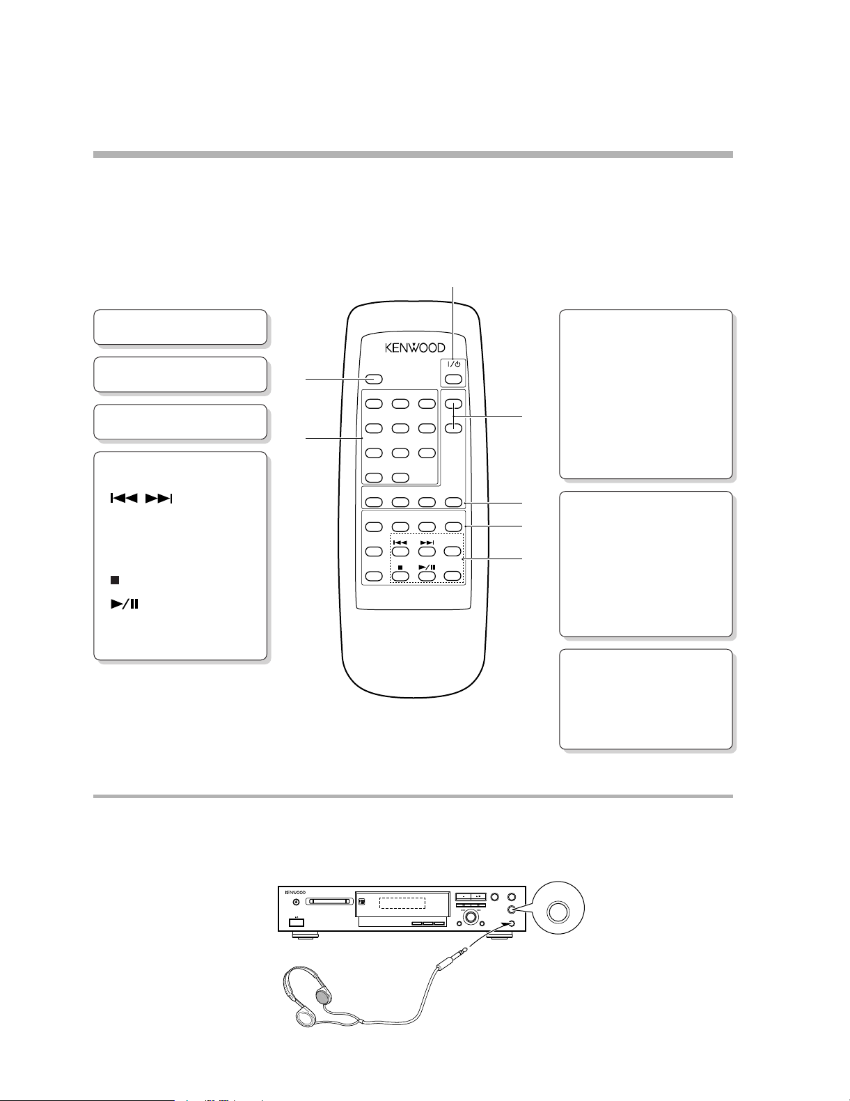
Remote control unit
POWER
DISPLAY
TIME
DISPLAY
6
1
9
+10
REC
MODE
PLAY
MODE
AUTO
MARK
REC
CANCEL
SYNCHRO
REC
REC
REC
INPUT
TRACK EDIT TIMERENTER
PROGRAM
CLEAR
EJECT
2 3
4 5
7 8
0
SELECT
REMOTE CONTROL UNIT
RC-M0301
7
6
5
4
3
2
1
4 Basic operation keys
/
: Skip down/ Skip up
(Cue/Review) key
REC : Record key
: Stop key
: Play/Pause key
PLAY MODE
: Play mode key
7 Display keys
DISPLAY : Display key
TIME DISPLAY : Time display
key
Model: RC-M0301
Infrared ray system
The remote control unit incorporates the basic operation keys as well as a variety of applied operation keys
so that it can be used in a wide range of purposes.
Use care to store the remote control unit in a safe place so as not to lose it.
1 POWER key
2 EJECT key
3 Numeric keys
6 Recording operation keys
REC INPUT: Input select key
REC MODE: Record mode key
AUTO MARK: Auto mark key
REC CANCEL: Record cancel
key
Plug the stereo headphones (with standard-plug) available in audio stores into the PHONES jack and adjust the listening volume
with the PHONES LEVEL control on the front panel.
Listening through headphones
5 Applied operation keys
ENTET: Entet key
TRACK EDIT: Edit key
TIMER: Timer key
SYNCHRO REC:
Synchro recording key
PROGRAM: Program key
DM-3090
CONTROLS
4
PHONES LEVEL
PHONES
MAX
MIN
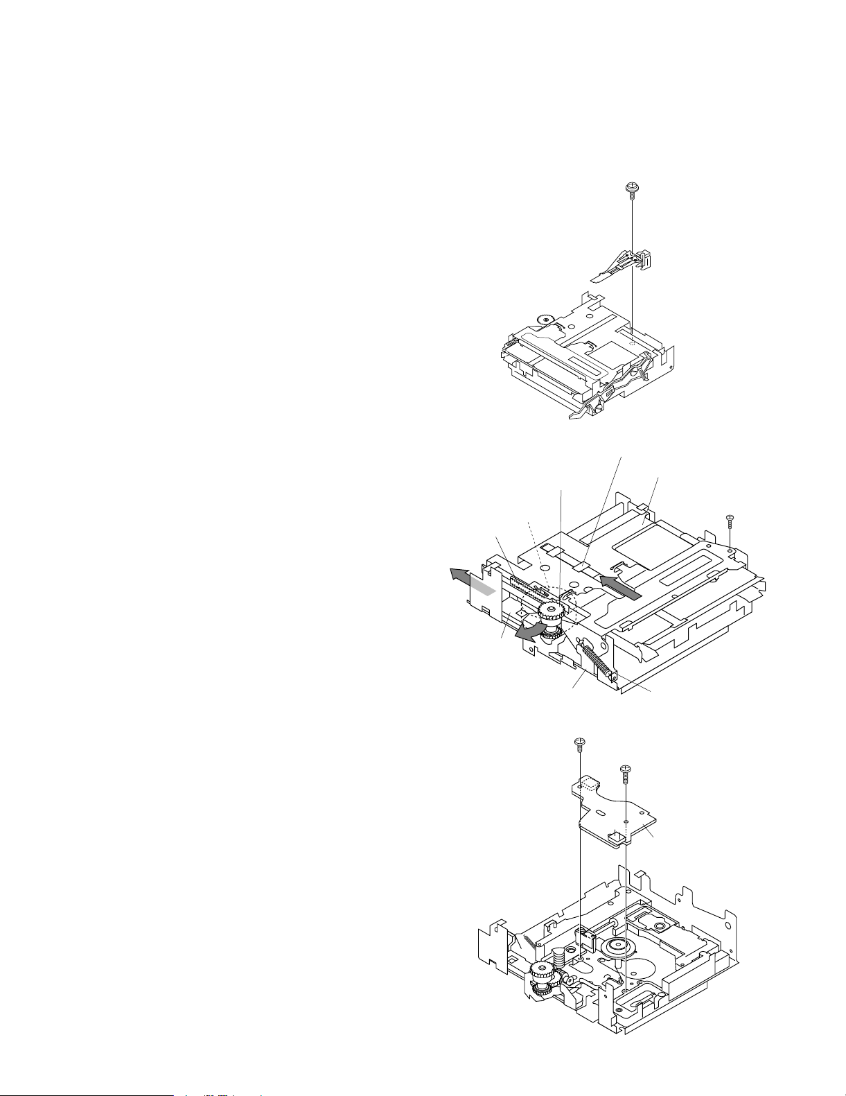
REMOVING AND REINSTALLING THE MAIN PARTS
MD MECHANISM SECTION
Perform steps 1 to 3 of the disassembly method to remove the
MD mechanism.
How to remove the magnetic head
(See Fig. 10-1)
1. Remove the screws (A1) x 1 pc.
10
Caution:
Take utmost care so that the magnetic head is not damaged
when it is mounted.
How to remove the cartridge holder
(See Fig. 10-2)
1. Open the roller arm lever in the arrow direction, and lower
the clamper lever to the rear side.
2. Apply +5V to the red line side of blue connector of loading
motor, push the rack gear in the arrow direction to move the
cam plate lever until tick is heard.
3. Remove the screw (B1) x1 pc., and the spring (B2) x1 pc.,
fitted to the holder arm, and shift the cartridge holder to the
left side to remove it.
How to remove the mechanism switch PWB
(See Fig. 10-3)
1. Remove the screws (C1) x 2 pcs., and remove the mechanism switch PWB.
Figure 10-1
Figure 10-2
Figure 10-3
DISASSEMBLY FOR REPAIR
DM-3090
(A1)x1
ø1.7x5mm
Magnetic Head
MD Mechanism
Loading Motor
Clampa Lever
Lack Gear
Roller Arm Lever
Cam Plate Lever
(C1)x1
Ø1.7x3mm
Slider Lever
Cartridge Holder
(B2) x1
(C1)x1
Ø1.7x9.5mm
MD Mechanism
Switch PWB
(B1) x1
Ø1.7x5mm
5
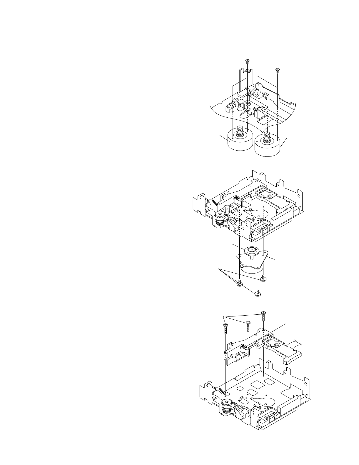
How to remove the sled motor/loading motor
(See Fig. 11-1)
1. Remove the screws (D1) x 1 pcs., and remove the sled
motor/loading motor.
Caution:
Be careful so that the gear is not damaged.
(The damaged gear emits noise during searching.)
Figure 11-1
Figure 11-2
Figure 11-3
How to remove the spindle motor
(See Fig. 11-2)
1. Remove the screws (E1) x 3 pcs., and remove the spidle
motor.
Caution:
Be careful so that the turntable is not damaged.
How to remove the optical pickup
(See Fig. 11-3)
1. Remove the screws (F1) x 3 pcs.
Caution:
Be careful so that the gear is not damaged.
(The damaged gear emits noise during searching.)
DM-3090
DISASSEMBLY FOR REPAIR
Loading
Motor
Turntable
(D1)x2
Ø1.7x2mm
(D1)x2
Ø1.7x2mm
Sled Motor
(E1)x3
Ø1.7x2.5mm
(F1)x3
Ø1.7x9.5mm
Spindle Motor
Optical Pickup
6
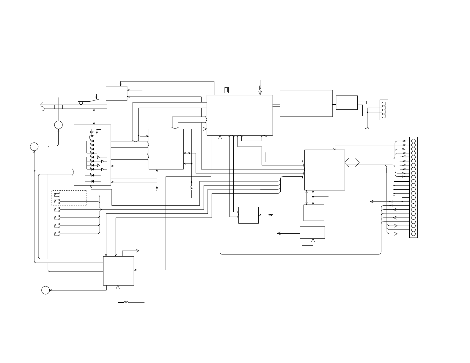
Figure 28BLOCK DIAGRAM (1/2)
D6.5/4.75 ~ 5.25V
MECHAN1SM
6.5/4.75~5.25V
D3.2V
SYSCLK
DVDD
DVDD
D3.2V
DIGITAL
3.2V
D3.2V
D4.3V
D4.3V
D3.2V
D4.3V
D3.2V
BACKUP
VOLTAGE
REGULATOR
POWER
IC1402
S29294A
E
2
PROM
IC1601
M56758FP
5-CH
MOTOR
DRIVER
BACKUP
MD MICRO COMPUTER
IC1401
IX0227AW
MD SYSTEM
MICRO
COMPUTER
DIGIN(EIAJ)
PDOWN
DIGOUT(EIAJ)
GND
GND
1
2
4
3
BCLK
MUTE
DFS0
DADATA
LRCLK
ADDATA
DFS1
LOAD IN
RESET
MD-ST
DSCK
SERCH
1
2
24
23
22
21
20
19
18
17
16
15
14
4
5
6
7
8
9
13
10
11
12
3
D.GND
D.GND
D.GND
D.GND
DSTB
MDDATA
KDATA
4M
DRAM
ENDEC
ATRAC
IC1201
LR37648
OSCILLATOR
XL1201
(33.8688MHz)
SW1956
SW1955
SW1954
SW1953
SW1952
Q1251~Q1254
MD
RECORDING HEAD
M901
SPINDLE MOTOR
M902
SLED MOTOR
M903
LOADING SWITCH
RECSWITCH
PLAYSWITCH
LEAD INSWITCH
A–BSIGNALE–FSIGNAL
RF1 ~ RF4SIGNAL
HEAD DRIVE
SIGNAL
IC1251
IC1101
IR3R55
RF
SIGNAL
PROCESSOR
LOADING MOTOR
HEAD UP/DOWN
M
M
DIRECT SWITCH
WRITE PRO
M
LASER DIODE
MONITOR DIODE
RF4
RF3
RF2
RF1
LIGHT
RECEIVING
SECTION
ERROR
SIGNAL
LIGHT
RECEIVING
SECTION
RF
F
A
B
E
FOCUS
TRACKING
PICK UP UNIT
IC1202
IX2474AF
CNP1904
CNP1902
IC1906
AND GATE TC7ST08F
IC1907
CLOCK GENERATOR TC92ASF
IC1990
INVERTOR 74AC04FS
IC1916
AND GATE
74VHC08F
BLOCK DIAGRAM
DM-3090
7
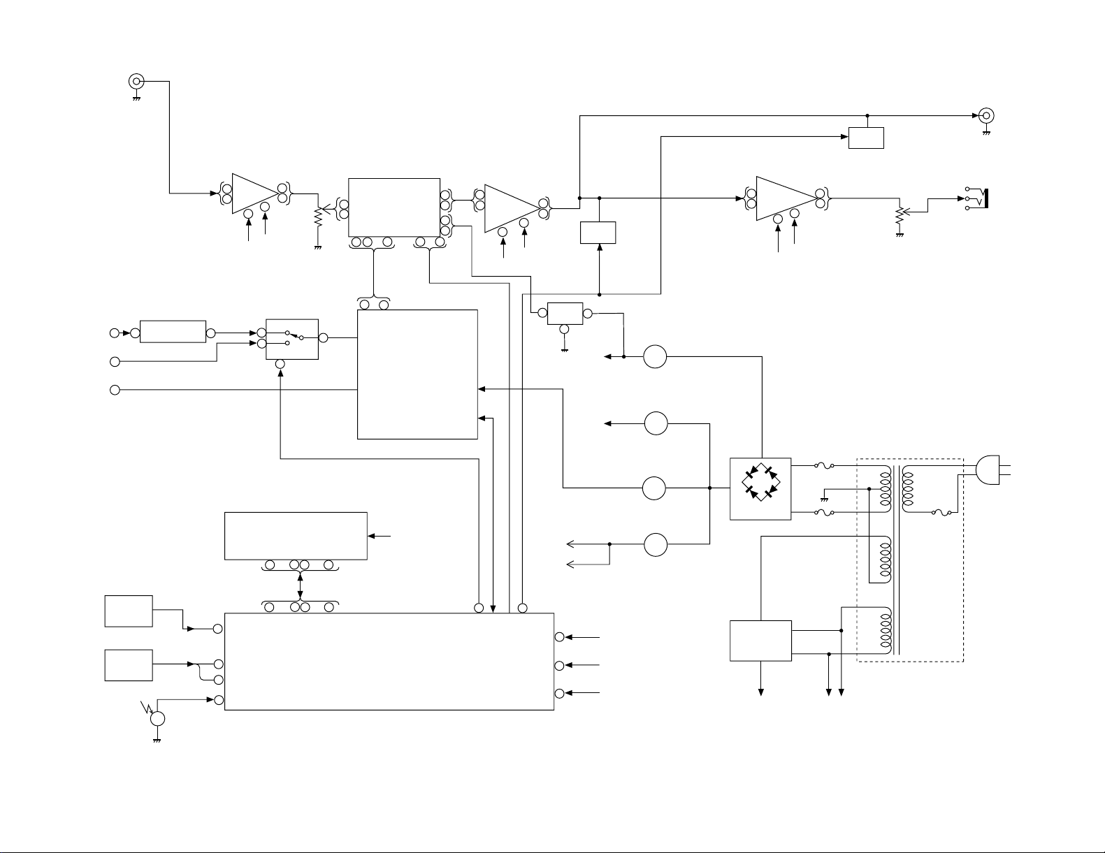
Figure 29BLOCK DIAGRAM (2/2)
LINE IN
J101
IC101
NJM4560D
OPE AMP
+7V
+7V
-7V
-7V
REC VOL
VR901
SYSCLK
AD DATA
LRCLK
BLCK
DA DATA
MODE
CLK
DATA
Q601
Q602
IC501
REGULATOR
S81233YK
J301
DIGITAL -IN
(COAXIAL JACK)
SO302
DIGITAL IN
(OPTICAL JACK)
RX302
DIGITAL OUT
(OPTICAL JACK)
IC301
74HCU04
INVERTER
IC302
NAND GATE
74HC10AP
DIGITAL IN
MD UNIT
DIGIN VCC
DIGITAL OUT
Q503
A-7V
POWER
CIRCUIT
MD+
POWER
CIRCUIT
5V SYSTEM
POWER
CIRCUIT
BACK UP 5V
DIGITAL 5V
MD 5V
MD+
S-ID,SYN,RESET,DSTB,DSCK
K-DATA,MD DATA
FL DISPLAY +B
FL901
~ ~
~ ~
DIG
SEG
JOG
KEY
RX-IN
IC901
IX0196AW
SYSTEM
MICROCOMPUTER
MD
MUTE
SW901
JOG
SWITCH
KEY IN
BLOCK
UN970
REMOTE
SENSOR
FL VP(-31V)
A/D +5V
BACK UP +5V
FL
POWER
CIRCUIT
FL VP(-32V)
FL DISPLAY +B
RECTIFYING
CIRCUIT
F551
1A L 250V
F552
1A L 250V
T551
POWER TRANSFORMER
AC 230V
50Hz
HEADPHINES
J981
H.P.VOL
VR981
IC651
NJM4560D
OPE AMP
Q451
Q452
MUTE
J101
LINE OUT
3
4
5
1
7
8
3
5
121916
13
15
24
26
10
2
3
4
5
1
7
2
1
3
8
3
4
5
1
7
8
8
13
2
6
13
10
17
21
21
42
60 89
45
90
92 97
2
3
6
32
10
33
96
91
100
~
~
+7V
-7V
IC201
UDA1340
AD/DA
CONVERTER
IC601
LINE AMP.
NJM4580D
Q502
Q506
Q504
A+7V
POWER
CIRCUIT
3V
~
8
DM-3090
BLOCK DIAGRAM

1 RF1 I
I
I
I
I
I
I
I
I
I
I
I
I
I
O
O
O
O
O
O
O
O
O
I
O
O
O
O
–
–
–
–
–
–
–
–
–
–
I
–
I
O
O
O
O
–
O
O
RF signal input terminal 1 Input of RF signal output of pickup
2 RF2 RF signal input terminal 2 Input of RF signal output of pickup
3 RF3 RF signal input terminal 3 Input of RF signal output of pickup
4 RF4 RF signal input terminal 4 Input of RF signal output of pickup
5 REFI Reference voltage amp. input terminal
6 REFO Reference voltage amp. output terminal
7 RFADD RF1 to 4 resistance addition output terminal
8 TCGI Track cross detection signal amp. input terminal for groove
9 AIN Servo signal amp. (focus servo system) inversion input terminal
10 BIN Servo signal amp. (focus servo system) inversion input terminal
11 EIN Servo signal amp. (tracking servo system) inversion input terminal
12 FIN Servo signal amp. (tracking servo system) inversion input terminal
13 BIAS Bias input terminal
14 AVCC Analog section power terminal
15* VSTBY Logic signal output terminal (STBY signal inversion signal is output.)
16* XDISC Logic signal output terminal (DISC signal inversion signal is output.)
17* XSGAIN Logic signal output terminal (SGAIN signal inversion signal is output.)
18 AGND Analog section GND terminal
19 DGND Digital section GND terminal
20 DTEMP Chip temperature detection terminal
21 LATCH Latch signal input terminal
22 CLOCK Clock signal input terminal
23 DATA Serial data input terminal
24 DVCC Digital section power terminal
25 FOUT Servo signal amp. (tracking servo system) output terminal
26 EOUT Servo signal amp. (tracking servo system) output terminal
27 BOUT Servo signal amp. (focus servo system) output terminal
28 AOUT Servo signal amp. (focus servo system) output terminal
29 TCGO Track cross detection signal amp. output terminal for groove
30 WBO Comparator output terminal for ADIP signal binary-coding
31 22KI Comparator input terminal for ADIP signal binary-coding
32 22KO ADIP signal HPF amp. output terminal
33 ADLPFO ADIP signal LPF amp. output terminal
34* NC NC
35 ADIPO ADIP signal primp. output terminal
36 ADIPI ADIP signal AGC amp. output terminal
37 ADAGC ADIP signal AGC smoothing capacitor connection terminal
38 ADAGI ADIP signal AGC amp. input terminal
39 RF2-1 RF1 and RF2 difference signal
40 EFMO RF signal primp. output terminal
41* WFMI RF signal AGC amp. output terminal
42 AVCC Analog section power terminal
43 AGND Analog section GND terminal
44 EFMAGC EFM signal AGC smoothing capacitor connection terminal
45 EFMAGI EFM signal AGC amp. output terminal
46* ATTR Pins 47 and 48 output signal attenuation terminal
47 GOUT Output of signal of RF1+RF2-RF3-RF4 for groove
48 POUT Rf1 to 4 resistance addition output for pit
IC1101 VHiiR3R55//-1:RF Signal Control (IR3R55)
Pin No.
Terminal Name I/O
Function
In this unit, the terminal with asterisk mark (*) is (open) terminal which is not connected to the outside.
CIRCUIT DESCRIPTION
DM-3090
9
DM-3090
1* EFMMON Output EFM monitor output
2 AVCC — Analog power
3 EFMI Input EFM signal input from RF amp.
4 AGND — Analog GND
5 AIN Input Focus error signal A
6 EIN Input Tracking error signal E
7 TCG Input Track cross signal
8 BIN Input Focus error signal B
9 FIN Input Tracking error signal F
10* VBAT Input Power voltage detection signal for constant voltage servo
11 WBI Input ADIP wobble signal
12 VDD1 — Digital power
13 DGND — Digital GND
14,15 TEST0,TEST1 Input Input for test. Connection to GND in case of normal use
16 TEST2 Input Input for test. Endecode/servo mode and ATRAC mode selection
17 X176KO Output Clock output. f=176.4 kHz (4fs)
18 FODRF Output Focus servo forward output. PWM
19 FODRR Output Focus servo reverse output. PWM
20 TRDRF Output Tracking servo forward output. PWM
21 LATCH Output Tracking servo reverse output. PWM
22 CLOCK Output Slide servo forward output. PWM
23 DATA Output Slide servo reverse output. PWM
24 DVCC Output Spindle servo forward output or spindle servo output. PWM
25 FOUT Output Spindle servo reverse output or spindle rotation (forward/reverse)selection
26 EOUT Output Address output to external D-RAM. ADR3
27 BOUT Output Address output to external D-RAM. ADR2
28 AOUT Output Address output to external D-RAM. ADR1
29 TCGO Output Address output to external D-RAM. ADR0 (LSB)
30* WBO Output Address output to external D-RAM. ADR10 (MSB)
31 22KI — Power supply for DRAM interface
32 22KO Output Address output to external D-RAM. ADR4
33 ADLPFO Output Address output to external D-RAM. ADR5
34 NC Output Address output to external D-RAM. ADR6
35 ADIPO Output Address output to external D-RAM. ADR7
36 ADIPI Output Address output to external D-RAM. ADR8
37 ADAGC Output Data output enable signal output to external D-RAM
38 ADAGI — Digital GND
39 RF2-1 Output Column address strobe signal output to external D-RAM
40 EFMO In/Output Data input/output from and to external D-RAM. D2
41 WFMI In/Output Data input/output from and to external D-RAM. D3 (MSB)
42 AVCC Output Data input/output from and to external D-RAM. ADR9
43 AGND Output Low address strobe signal output to external D-RAM
44 EFMAGC Output Data write enable signal output to external D-RAM
45 EFMAGI In/Output Data input/output from and to external D-RAM. D1
46 ATTR In/Output Data input/output from and to external D-RAM. D0 (LSB)
47* GOUT Output Track cross signal
48* POUT Output ADIP CRC error flag monitor output
49* PLCK Output EFM PLL clock output in playback mode
50 EFM0 Output EFM signal output in record mode. C1F (C1 error flag) monitor output in playback mode
51* X700KO Output Clock output. f = 705.6 kHz. Clock output is not performed when RSTX = 0.
52* EXPORT0 Output Microcomputer extension output port 0
53* EXPORT1 Output Microcomputer extension output port 1
IC1201 VHiLR37648/-1:ENDEC/ATRAC (LR37648)
Pin No.
Terminal Name
Function
In this unit, the terminal with asterisk mark (*) is (open) terminal which is not connected to the outside.
Input/Output
CIRCUIT DESCRIPTION
10

54 TESO1 Output PLLLR. Microcomputer extension output port 2 in case of selection
55 TESO3 In/Output PLLOSC. Microcomputer extension output port 3 in case of selection
56 TEST4 In/Output EXTCLK. Microcomputer extension output port 4 in case of selection
57 CDDATA In/Output
High speed dubbing CD data input. Microcomputer extension output port 5 in case of selection
58 CDLRCK In/Output
High speed dubbing CD LR data input. Microcomputer extension output port 6 in case of selection
59 CDBCLK In/Output
High speed dubbing CD bit data input. Microcomputer extension output port 7 in case of selection
60 VXI Input Vari-pitch PLL clock input
61 VPO Output Vari-pitch PLL phase error output
62 VDD1 — Digital power
63 DGND — Digital GND
64 XI Input Oscillation circuit input. 33.8688 MHz
65 XO Output Oscillation circuit input. 33.8688 MHz
66 DIN Input Digital input signal
67 DOUT Output Digital output signal
68 VDD3 — Power for internal PLL
69 DGND — Digital GND
70 LRCK Output Music data Lch/Rch selection output
71 BLCK Output Music data shift clock
72 DFCK Output AD/DA converter digital filter clock. 256 Fs
73 ADDATA Input Audio data input
74 DADATA Output Audio data output
75* FEMON Output Focus error signal monitor output
76* TOTMON Output Total signal monitor output
77* TEMON Output Tracking error signal monitor output
78* SBCK Input DIN subcode read clock. EIAJ CP-309 Format
79* SBO Output DIN subcode serial data. EIAJ CP-309 Format
80* SBSY Output DIN subcode block sync signal. EIAJ CP-309 Format
81 SFSY Output DIN subcode frame sync signal. EIAJ CP-309 Format
82 FOK Output Focus OK detection signal. "0" : Focus OK
83 SENSE Output Servo status detection signal. "1": Auto-move, auto-jump, auto-focus retraction
84 COUT Output Track cross signal output
85 MCCK Output Microcomputer clock output. Clock output is performed also when RSTX = 0.
86 DINTX Output System controller interface interruption request output terminal
87 VDD1 — Digital power
88 DGND — Digital GND
89 RSTX Input Chip reset input. "L": Reset
90 SYD0 In/Output System controller interface data bus terminal (LSB)
91~96 SYD1~SYD6 In/Output System controller interface data bus terminal
97 SYD7 In/Output System controller interface data bus terminal (MSB)
98 SYWRX Input System controller interface register writing pulse input
99 SYRDX Input System controller register read pulse input
100 SYRS Input System controller interface register selection input
Pin No.
Terminal Name
Function
In this unit, the terminal with asterisk mark (*) is (open) terminal which is not connected to the outside.
Input/Output
CIRCUIT DESCRIPTION
DM-3090
11

1* P96/ANEX1 Output Not used
2* P95/ANEX0 Output Not used
3 P94/DA1 Output LDVAR (laser power adjustment output)
4* P93/DA0 Output ADJS (for automatic adjustment step check)
5* P92/TB2IN Output Not used
6 P91/TB1IN Input LD SW CK input (interruption input only in single state)
7 P90/TB0IN Input ERR input (monitor PLL UNLOCK)
8 BYTE Input GND
9 CNVss Input GND
10* P87/XCIN Output ST-ID Output
11* P86/XOUT Output MD search output
12 RESET Input RESETInput
13* XOUT — Extal clock output
14 Vss — GND
15 XIN Input EXTAL (8.4672 MHz)
16 Vcc — + 3.15V
17 P85/NMI Input Connect +B
18 P84/INT2 Input DINT (interruption input from MD LSI)
19 P83/INT1 Input DSENSE (servo sense input from MD LSI)
20 P82/INT0 Input ST-ID Input (MD-ON)
21 P81/TA4IN Input CD search input (syncro REC suspension input from MD LSI)
22 P80/TA4OUT Output MD RSW Output
23* P77/TA3IN Input FSW1 (SW power frequency selection)
24 P76/TA3OUT Output Vari-pitch correspondence given (H)/not given (L)
25 P75/TA2IN Input P-DOWN (power failure detection)
26 P74/TA2OUT Output HDON (magnetic head current ON/OFF output)
27 P73/TA1IN Output LD+ (loading motor + control output)
28 P72/TA1OUT Output LD- (loading motor + control output)
29 P71/TA0IN Input CIN (track count signal input)
30 P70/TA0OUT Input INN SW (inner SW detection input)
31 P67/TXD1 Output R-DATA
32 P66/RXD1 Output R-LATCH
33 P65/CLK1 Output R-CLK
34
P64/CTS1/RTS1/
Output DSTB (system controller communication enable and communication beingexecuted)
CTS0/CLKS1
35 P63/TXD0 Output MD DATA (MD Data Output)
36 P62/RXD0 Input K DATA (system controller data input)
37 P61/CLK0 Input DSCK (system controller communication clock input)
38
P60/CTS0/RTS0
Input 4M/16M DRAM selection input
39
P57/RDY/CLK
OUT
Output R/P output (REC/PLAY selection)
40 P56/ALE Input FOK (focus servo status monitor input)
41* WFMI Input/Output Not used
42 AVCC Output S2 Ouput
43 AGND Output S1 Output
44 EFMAGC Output SYRS (MD-LSI register selection signal output)
45 EFMAGI Output SYRD (MD-LSI read signal output)
46 ATTR Output SYWR (MD-LSI right signal output)
47 GOUT In/Output SYS D7 (data bus 7)
48 POUT In/Output SYS D6 (data bus 6)
49 PLCK In/Output SYS D5 (data bus 5)
50 EFM0 In/Output SYS D4 (data bus 4)
51 X700KO In/Output SYS D3 (data bus 3)
IC1401 RX-iX0227AWZZ:MD System Microcomputer (IX0227AW)
Pin No.
Terminal Name
Function
In this unit, the terminal with asterisk mark (*) is (open) terminal which is not connected to the outside.
Input/Output
DM-3090
CIRCUIT DESCRIPTION
12

52 P42/A18 In/Output SYS D2 (data bus 2)
53 P41/A17 In/Output SYS D1 (data bus 1)
54 P40/A16 In/Output SYS D0 (data bus 0)
55* P37/A15 Output Not used
56* P36/A14 Output Not used
57* P35/A13 Output Not used
58 P34/A12 Output EEPRO (EEPROM protection cancel)
59 P33/A11 Output EPCS (EEPROM chip selector output)
60 P32/A10 In/Output EEPD (EEPROM sirial data output)
61 P31A9 Output EEPK (EEPROM sirial colck output)
62 Vcc Input + 3.15V
63* P30/A8 Output Not used
64 Vss — GND
65* P27/A7 Output L3 DATA (soft serial communication, 2 modes provided, LSB fast)
66* P26/A6 Output L3 MODE (soft serial communication, 2 modes provided, LSB fast)
67* P25/A5 Output L3 CLK (soft serial communication, 2 modes provided, LSB fast)
68* P24/A4 Output Not used
69* P23/A3 Output Not used
70 P22/A2 Output PCNT0 output
71* P21/A1 Output Not used
72 P20/A0 Output LDON output (H: ON)
73 P17/D15 Output ANLPTR output
74* P16/D14 Output ADPON output (for CK)
75* P15/D13 Output DAPON output (for CK)
76 P14/D12 Output DFS0 output
77 P13/D11 Output DFS1 output
78* P12/D10 Output DIG EX output (for CK)
79* P11/D9 Output DIG CD output (for CK)
80 P10/D8 Output XRST (system reset output)
81* P07/D7 Output AD MUTE output (for CK)
82* P06/D6 Output EMPHA output (for CK)
83* P05/D5 Output DA MUTE output (for CK)
84 P04/D4 Output MUTE output
85* P03/D3 Output DOUTM output (for CK)
86 P02/D2 Input TEST2 (special mode selection 2)
87 P01/D1 Input TEST1 (special mode selection 1)
88 P00/D0 Input TEST0 (special mode selection 0)
89 P107/AN7/KI3 Input AVCK3 (special mode monitor input)
90 P106/AN6/KI2 Input AVCK2 (AD/DA section 3.1V monitor input)
91 P105/AN5/KI1 Input AVCK1 (DOUT section 5V monitor input)
92 P104/AN4/KI0 Input DTEMP (temperature detection input)
93 P103/AN3 Input MINF (disc type/REC input)
94 P102/AN2 Input TEST K1 (test key input 1)
95 P101/AN1 Input TEST K2 (test key input 2)
96 AVss — GND
97 P100/AN0 Input HINF (mechanism position/HEAD position)
98 VREF — + 3.15V
99 AVcc — + 3.15V
100 P97/ADTRG Input Connect +B
Pin No.
Terminal Name
Function
In this unit, the terminal with asterisk mark (*) is (open) terminal which is not connected to the outside.
Input/Output
CIRCUIT DESCRIPTION
DM-3090
13

DM-3090
IC901 RH-iX0196AFZZ: System Control Microcomputer (iX0196AW)
Pin No.
FunctionPort Name
Input/Output
Terminal Name
In this unit, the terminal with asterisk mark (*) is (open) terminal which is not connected to the outside.
1* P77/AN7 KEY1 Output Not used
2 P76/AN6 KEY2 Input Key entry
3 P75/AN5 KEY3 Input Key entry
4* P74/AN4 — Output Not used
5 P73/AN3 INI Input Initial setting entry
6 P72/AN2 JOG_AD Input Jog dial entry
7*,8* P71/AN1,P70/AN0 — Output Not used
9* PB3 — Output Not used
10 PB2/DA DIG SEL1 Output Digital signal selector selection signal
11* P57/SRDY3/AN15 DIG SEL2 Output Not used
12* P56/SCLK3/AN14 — Output Not used
13* P55/SOUT3/AN13 — Output Not used
14 P54/SIN3/AN12 DAC_MODE Output Externally provided DAC/ADC serial interface mode signal
15 P52/SRDY2/AN11 DAC_CLK/EX Output Externally provided DAC/ADC serial interface clock signal
16 P52/SCLK2/AN10 DAC_DATA/EX Output Externally provided DAC/ADC serial interface clock signal
17* P51/SOUT2/AN9 — Output Not used
18 P50/SIN2/AN8 DFS0/DFS1 Input EMPHASIS information from MD
19 P67/SRDY1/CS/ DSTRB Input MD serial interface strobe signal
SCLK12
20 P66/SCLK1 DSCK Output MD serial interface clock signal
21 P65/SOUT1 K-DATA Output MD serial interface transmission signal
22 P64/SIN1 MD-DATA Input MD serial interface reception signal
23 P63/CNTR1 MD-LO/EJ Output MD loading power voltage selection signal
24* P62/CNTR0 — Output Not used
25* P61/PWM — Output Not used
26* P60 — Output Not used
27* P47/T3OUT — Output Not used
28* P46/T1OUT — Output Not used
29 P45/INT1/2CR P IN Input Power failure detection
30* P44/INT4 P.CNT Output Power control
31 P41 P-OUT Output MD power failure detection signal
32 P42/INT2 RX-IN Input Remote control loght reception signal
33 P41 P-MUTE Output Audio mute control signal
34 P40/INT0 — Input GND
35 RESET RESET Input RESET signal entry
36 PB1/Xcin Xcin Input Sub clock IN connection (32.7k)
37 PB0/Xcout Xcout Output Sub clock OUT connection (32.7k)
38 Xin Xin Input Main clock IN connection (8M)
39 Xout Xout Output Main clock OUT connection (8M)
40 VSS VSS Input GND
41 P27 SERCH Output CD to MD search monitor signal
42 P26 LOAD Input MD loading detection
43 P25 S-ID Output CD to MD start ID signal
44 P24 MD RESET Output RESET signal to MD
CIRCUIT DESCRIPTION
14

CIRCUIT DESCRIPTION
Pin No.
FunctionPort Name
Input/Output
Terminal Name
72-80 P97/SEG23- S0-S8 Output Segment for FL drive
P90/SEG16
81-88 P87/SEG15- S9-S16 Output Segment for FL drive
P80/SEG8
89,90 PA7/SEG7, S17,S18 Output Segment for FL drive
PA6/SEG6
91 VCC VCC Input +5V
92-97 PA5/SEG5- S19-S24 Output Segment for FL drive
PA0/SEG0
98 VEE VEE Input -30V
99 AVSS AVSS Input GND
100 VREF VREF Input +5V
45-54 P23/DIG19- UDIG0-UDIG9 Output Digit for FL drive
P12/DIG10
55,56 P11/SEG41/DIG9, UDIG10,UDIG11 Output Digit for FL drive
P10/SEG40/DIG8
57-60 P07/SEG39/DIG7- UDIG12-UDIG15 Output Digit for FL drive
P04/SEG36/DIG4
61-64 P05/SEG35/DIG3- S35-S32 Output Segment for FL drive
P00/SEG33/DIG0
65-72 P37/SEG31- S31-S25 Output Segment for FL drive
P30/SEG25
DM-3090
15
 Loading...