

Page 1
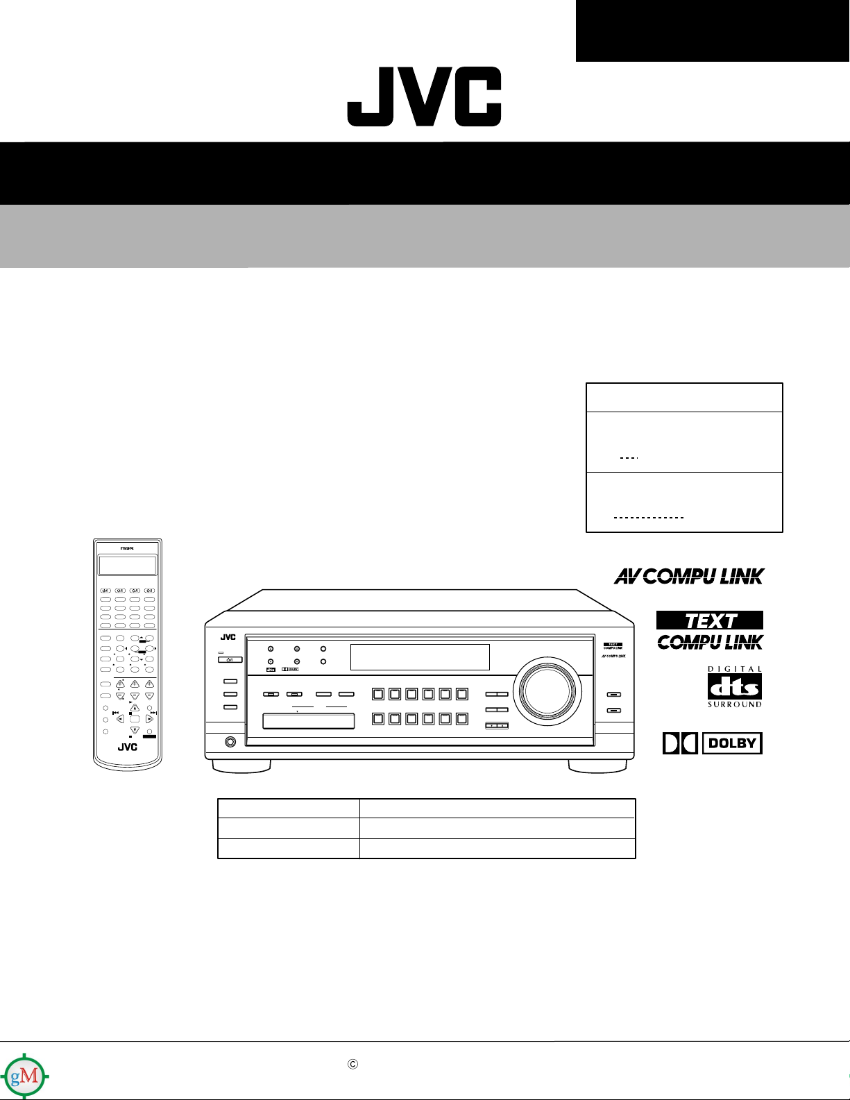
RX-8012VSL/RX-8010VBK
SERVICE MANUAL
AUDIO/VIDEO CONTROL RECEIVER
RX-8012VSL
CATV/DBS VCR 1 TV AUDIO
DVD MUILTIDVD
CD
CDR
TV/DBS VIDEO PHONO
VCR 1 VCR 2
TAPE/MD
DSP
ANALOG/DIGITAL
SURROUND
MODE INPUTON/OFF
LINE DIF.ECT BOOST EFFECT
231
MENU
MIDNIGHT
TEST CTR TONE
MODE
564
ENTER
SUBWFR
L/R BAL CENTER
SOUND
7/P
89
REAR L REAR R
DIGITAL EQ
MUTING
0 +1010
RETURN FM MODE 100
CATV/DBS
CONTROL
CONTROL
BAL L
LEVEL TV VOL
CH/
TV/VIDEO
BAL R
PLAY
MENU
TEXT
/REW
PAUSE
DISPLAY
SET
REC
DOWN – TUNING – UP
PAUSE
STOP
RM-SRX8012U
A/V CONTROL RECEIVER
LIVENESS
VOLUME
FF/
CONTROL
RX-8010VBK
Area Suffix
RX-8012VSL
UW Brazil,Mexico,Peru
RX-8010VBK
UJ U.S.Military
FM/AM
USB
SLEEP
ROOMBASS
SIZE
+
EXIT
SPEAKERS ON/OFF
SUBWOOFER OUT ON/OFF
PHONES
STANDBY
STANDBY/ON
1
2
FM/AM TUNING FM/AM PRESET FM MODE
DIGITAL
DIGITAL
SURROUND
SURROUND ON/OFF
USB AUDIO
S-VIDEO VIDEO
PUSH OPEN
MEMORY
INPUT
ANALOG/DIGITAL
INPUT ATT
VIDEO
L—AUDIO—R
RX-8012V AUDIO/VIDEO CONTROL RECEIVER
MIDNIGHT MODEDSP MODE
SOUCE NAME
TV SOUND/DBSVIDEOVCR 2VCR 1DVDDVD MULTI
SOUCE NAME
FM / AMUSB AUDIOTAPE / MDCDRCDPHONO
DIGITAL
EQ
EFFECT SETTING
CONTROL
DOWN UP
MASTER VOLUME
LEVEL
ADJUST
LINE DIRECT
BASS BOOST
DIGITAL
Model
RX-8012VSL
RX-8010VBK
Color
Silver
Black
Contents
Safety precautions -----------------------------------------------------------1-2
Disassembly method --------------------------------------------------------1-3
Adjustment method ----------------------------------------------------------1-9
Self-diagnose function -------------------------------------------------------1-10
Description of major ICs ----------------------------------------------------1-12~28
COPYRIGHT 2001 VICTOR COMPANY OF JAPAN, LTD.
No.21002
Jun. 2001
Page 2
http://getMANUAL.com
RX-8012VSL/RX-8010VBK
1. This design of this product contains special hardware and many circuits and components specially for safety
purposes. For continued protection, no changes should be made to the original design unless authorized in
writing by the manufacturer. Replacement parts must be identical to those used in the original circuits. Services
should be performed by qualified personnel only.
2. Alterations of the design or circuitry of the product should not be made. Any design alterations of the product
should not be made. Any design alterations or additions will void the manufacturer's warranty and will further
relieve the manufacture of responsibility for personal injury or property damage resulting therefrom.
3. Many electrical and mechanical parts in the products have special safety-related characteristics. These
characteristics are often not evident from visual inspection nor can the protection afforded by them necessarily
be obtained by using replacement components rated for higher voltage, wattage, etc. Replacement parts which
have these special safety characteristics are identified in the Parts List of Service Manual. Electrical
components having such features are identified by shading on the schematics and by ( ) on the Parts List in
the Service Manual. The use of a substitute replacement which does not have the same safety characteristics
as the recommended replacement parts shown in the Parts List of Service Manual may create shock, fire, or
other hazards.
4. The leads in the products are routed and dressed with ties, clamps, tubings, barriers and the like to be
separated from live parts, high temperature parts, moving parts and/or sharp edges for the prevention of
electric shock and fire hazard. When service is required, the original lead routing and dress should be
observed, and it should be confirmed that they have been returned to normal, after re-assembling.
5. Leakage current check (Electrical shock hazard testing)
After re-assembling the product, always perform an isolation check on the exposed metal parts of the product
(antenna terminals, knobs, metal cabinet, screw heads, headphone jack, control shafts, etc.) to be sure the
product is safe to operate without danger of electrical shock.
Do not use a line isolation transformer during this check.
Plug the AC line cord directly into the AC outlet. Using a "Leakage Current Tester", measure the leakage
current from each exposed metal parts of the cabinet, particularly any exposed metal part having a return
path to the chassis, to a known good earth ground. Any leakage current must not exceed 0.5mA AC (r.m.s.).
Alternate check method
Plug the AC line cord directly into the AC outlet. Use an AC voltmeter having, 1,000 ohms per volt or more
sensitivity in the following manner. Connect a 1,500 10W resistor paralleled by a 0.15 F AC-type capacitor
between an exposed metal part and a known good earth ground.
Measure the AC voltage across the resistor with the AC
voltmeter.
Move the resistor connection to each exposed metal part,
particularly any exposed metal part having a return path to
the chassis, and measure the AC voltage across the resistor.
Now, reverse the plug in the AC outlet and repeat each
measurement. Voltage measured any must not exceed 0.75 V
AC (r.m.s.). This corresponds to 0.5 mA AC (r.m.s.).
0.15 F AC TYPE
1500 10W
Good earth ground
AC VOLTMETER
(Having 1000
ohms/volts,
or more sensitivity)
Place this
probe on
each exposed
metal part.
!
1. This equipment has been designed and manufactured to meet international safety standards.
2. It is the legal responsibility of the repairer to ensure that these safety standards are maintained.
3. Repairs must be made in accordance with the relevant safety standards.
4. It is essential that safety critical components are replaced by approved parts.
5. If mains voltage selector is provided, check setting for local voltage.
Burrs formed during molding may
be left over on some parts of the
chassis. Therefore, pay attention to
such burrs in the case of
preforming repair of this system.
In regard with component parts appearing on the silk-screen printed side (parts side) of the PWB diagrams, the
parts that are printed over with black such as the resistor ( ), diode ( ) and ICP ( ) or identified by the " "
mark nearby are critical for safety.
When replacing them, be sure to use the parts of the same type and rating as specified by the manufacturer.
(Except the J&C version)
1-2
Page 3
RX-8012VSL/RX-8010VBK
Disassembly method
Removing the top cover (See Fig.1)
1.
Remove the four screws A attaching the top cover
on both sides of the body.
2.
Remove the three screws B on the back of the body.
3.
Remove the top cover from behind in the direction of
the arrow while pulling both sides outward.
Removing the front panel assembly
(See Fig.2 to 3)
Prior to performing the following procedure, remove
the top cover.
1.
Disconnect the card wire from connector CN400 on
the audio board and CN402 on the power supply
board in the front panel assembly.
2.
Cut off the tie band fixing the harness.
Tie band
Main
board
CN400
Top cover
A 2
A 2
C
B
Fig.1
Front panel assembly
C
CN402
Power
supply
board
3.
Remove the three screws C attaching the front panel
assembly.
4.
Remove the four screws D attaching the front panel
assembly on the bottom of the body. Detach the front
panel assembly toward the front.
Removing the voltage selector
(See Fig.4)
Prior to performing the following procedure, remove
the top cover.
1.
Remove the power cord stopper from the rear panel
by moving it in the direction of the arrow.
2.
Remove the two screws F' attaching the rear panel
on the back of the body.
Removing the rear panel (See Fig.4)
Prior to performing the following procedure, remove
the top cover.
Audio board
E
E
E
D
Fig.2
Front panel assembly
Fig.3
E
D
Cord stopper
1.
Remove the power cord stopper from the rear panel
by moving it in the direction of the arrow.
2.
Remove the thirty four screws E attaching the each
boards to the rear panel on the back of the body.
3.
Remove the three screws F attaching the rear panel
on the back of the body.
F
Rear panel
F
F'
F
E
Fig.4
1-3
Page 4
RX-8012VSL/RX-8010VBK
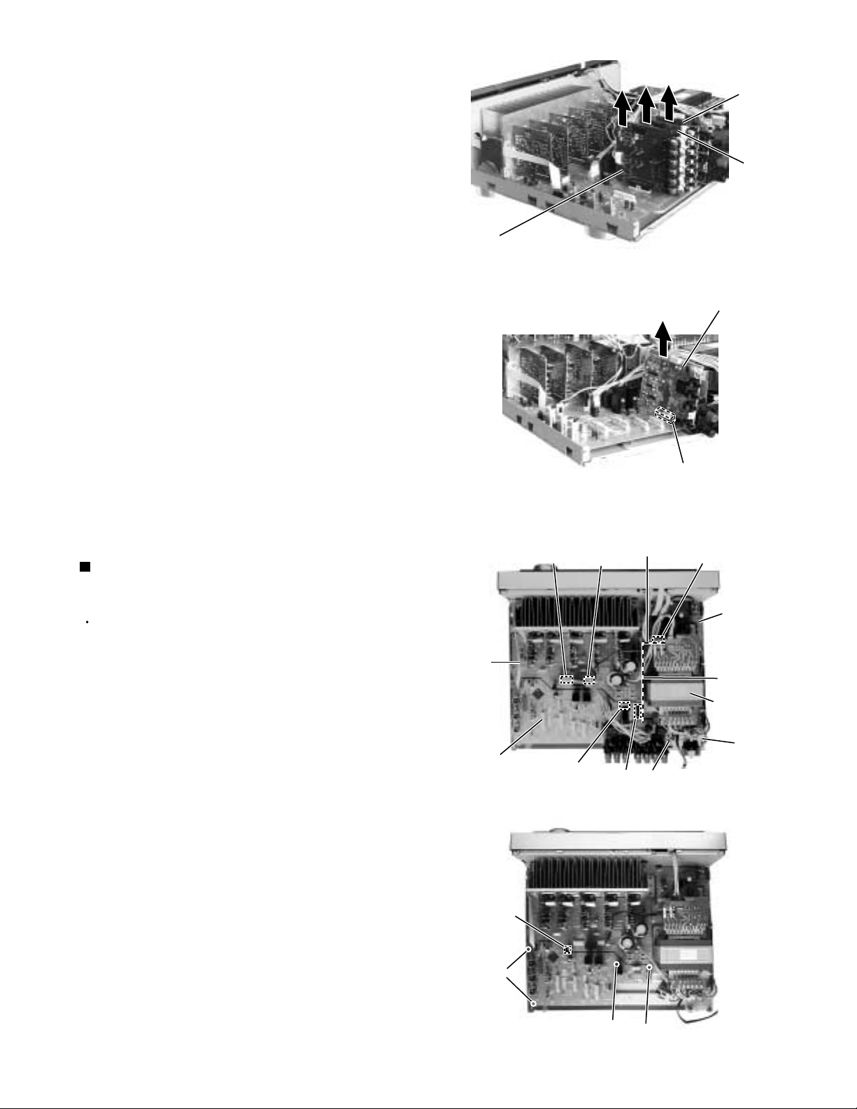
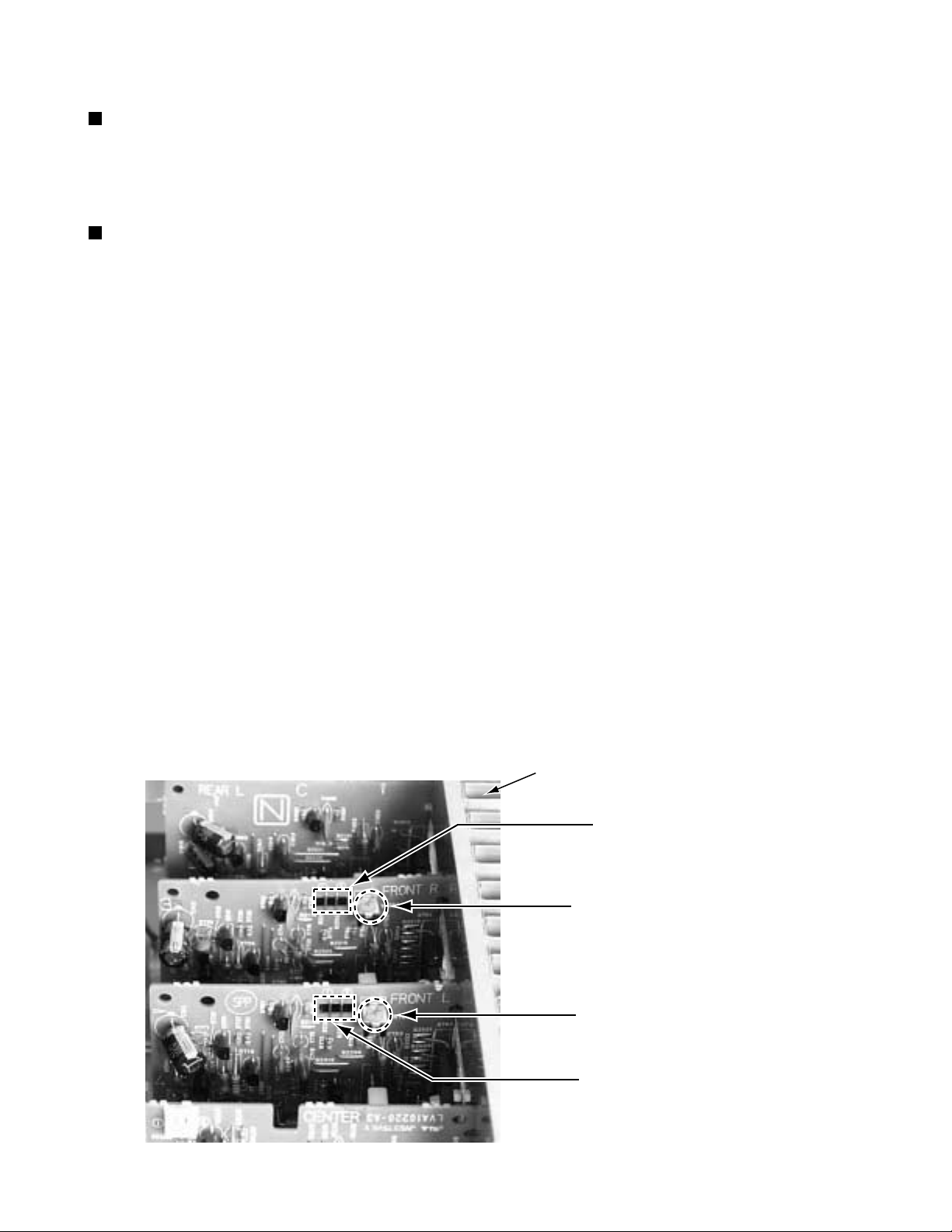
Removing each board connected to the
rear side of the audio board
(See Fig.5 to 11)
Prior to performing the following procedure, remove
the top cover and the rear panel.
1.
Cut off the tie band fixing the harness.
2.
Disconnect the connect CN501, CN243, CN205,
CN381, CN361 on the DVD board.
3.
Disconnect the harness from connector CN721,
CN722 and CN723.
4.
Disconnect the tuner board and audio input board
from connector CN101 and CN301 on the audio
board.
5.
Disconnect the video audio board and video board
from connector CN303 and CN201 on the audio
board.
6.
Disconnect the S video board from connector CN241
on the audio board.
CN361
CN381
CN723
CN731
CN732
CN205
CN243
Fig.5
CN721
Tie band
CN501
CN722
7.
Disconnect the DSP board from connector CN601 on
the audio board.
8.
Pull out the plastic pin which prevents from coming
out.
Audio board
CN416
CN206
Plastic pin
Audio input
board
Tuner
board
Video audio
board
Fig.6
Fig.7
Video
board
DVD board
S Video
board
DSP
board
1-4
CN101
CN301
CN303
CN201
CN241
Video audio
board
Fig.9
Video
board
S Video
board
CN244
CN101
Fig.8
Page 5
Video audio
board
RX-8012VSL/RX-8010VBK
S Video
board
Video
board
Fig.10
DSP board
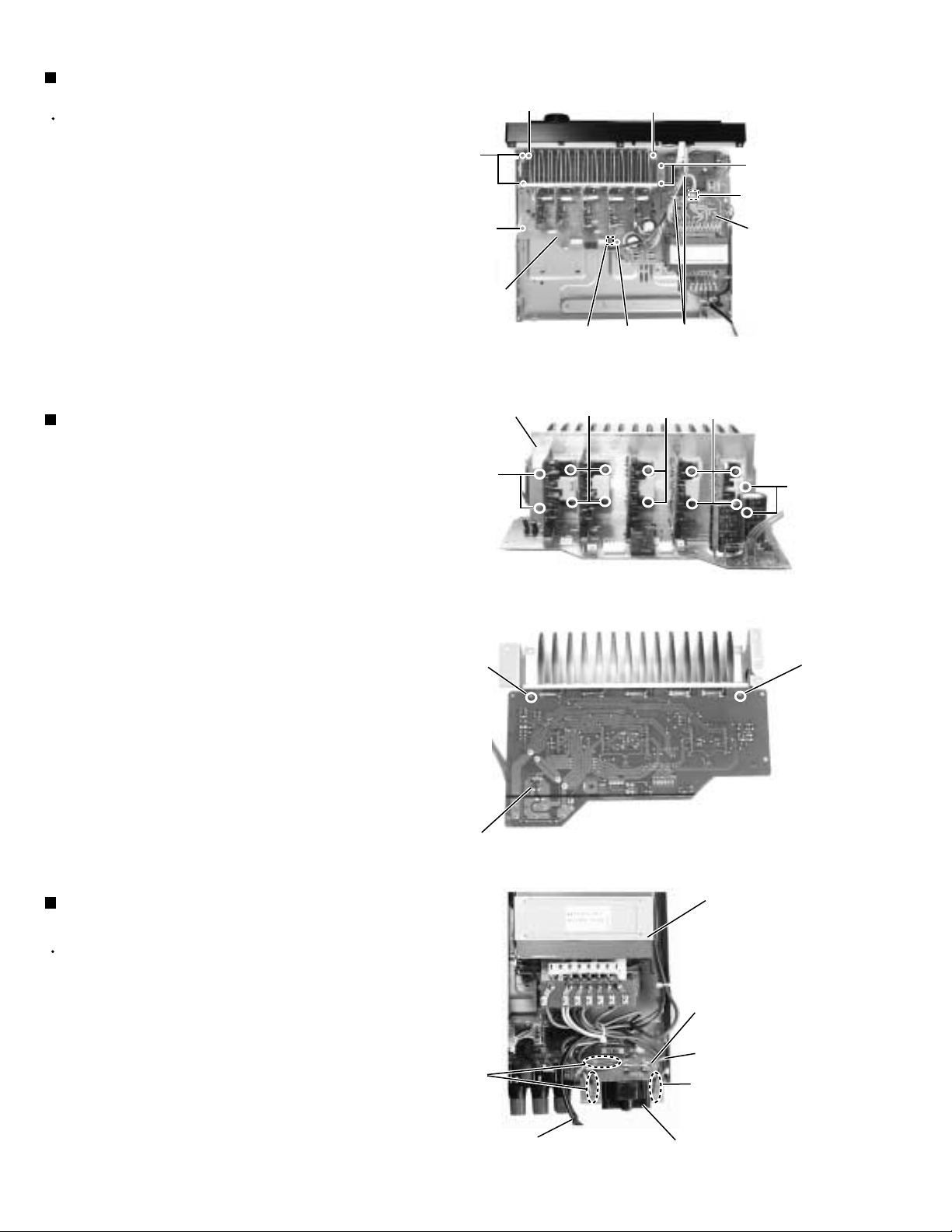
Removing the audio board
(See Fig.12 to 13)
Prior to performing the following procedure, remove
the top cover and the tuner board, audio input board,
video audio board, video board, S-video board, DVD
board and the rear panel.
Disconnect the harness from connector CN813 and
1.
CN814 on the main board.
Disconnect the card wire from connector CN931 and
2.
CN932 on the audio board.
Cut off the tie band fixing the harness.
3.
Disconnect the relay board from the audio board and
4.
the power supply board. (CN71,CN81)
Main
board
Audio board
CN814
CN931/ 932
CN813
Fig.11
CN81
Fig.12
CN601
Relay board
Power / Fuse
board
CN71
Power
supply
board
Tie band
Power
transformer
Voltage
select
board
Disconnect the card wire from connector CN831 on
5.
the main board.
Remove the three screws G attaching the audio
6.
board.
Remove the screw H attaching the audio board .
7.
CN831
G
G
Fig.13
H
1-5
Page 6
RX-8012VSL/RX-8010VBK
Removing the main board (See Fig.14)
Prior to performing the following procedure, remove
the top cover, the rear panel and audio board.
1.
Cut off the tie band fixing the harness.
2.
Disconnect the harness from connector CN811 on
the power supply board respectively.
3.
Disconnect the harness from connector CN881 on
the main board.
4.
Remove the four screws I and the four screws J
attaching the main board.
J
I
Main
board
I
I
J
CN811
Power
supply
board
CN881
Fig.14
I
Tie band
Removing the heat sink
(See Fig.15 to 16)
1.
Remove the ten screws K and four screws L
attaching the heat sink.
2.
Remove the two screws L' attaching the heat sink
from the rear side of main board.
Heat sink
L
L'
Main board
rear side
K
Fig.15
Fig.16
K
K
L
L'
Removing the voltage select board
(See Fig.17)
Prior to performing the following procedures, remove
the top cover and the rear panel.
1.
Cut off the tie band fixing the harness.
2.
Unsolder the six harnesses connected to the power
transformer.
1-6
Solder
points
Power cord
Power transformer
Voltage select board
Tie band
Solder points
Voltage selector
Fig.17
Page 7
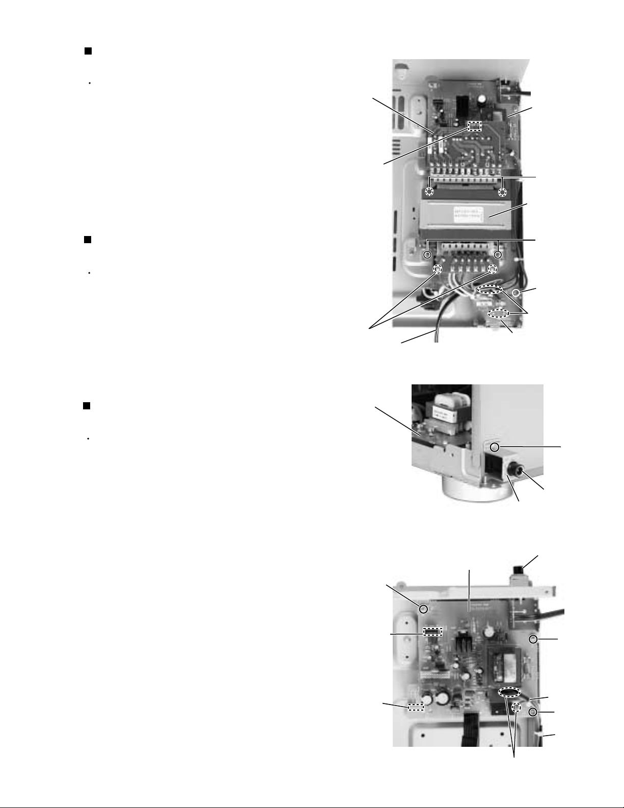
Removing the power transformer
(See Fig.18)
Prior to performing the following procedures, remove
the top cover.
1.
Unsolder the two harnesses connected to the power
transformer.
2.
Disconnect the harness from connector CN55 and
CN56 on the power transformer board.
3.
Remove the four screws M attaching the power
transformer.
Power
transformer
board
CN55 / 56
RX-8012VSL/RX-8010VBK
Power
supply
board
M
Power
transformer
Removing the power / fuse board
(See Fig.18)
Prior to performing the following procedure, remove
the top cover and the rear panel.
1.
Remove the screw N attaching the power / fuse
board.
2.
Unsolder the power cord and other harnesses
connected to the power / fuse board.
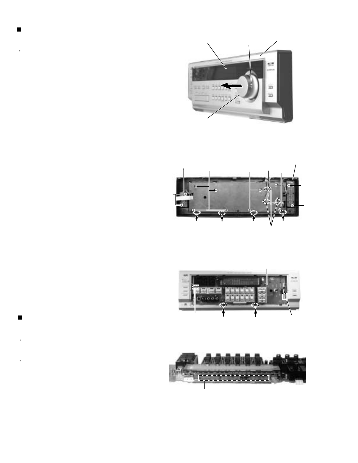
Removing the power supply board
(See Fig.19 to 21)
Prior to performing the following procedure, remove
the top cover and the front panel.
1.
Remove the screw O fixing a bonding ground.
2.
Remove the one nut attaching the headphone jack of
the power supply board on the front side of the body.
Solder points
Power cord
Power supply
board
Fig.18
Fig.19
M
N
Solder points
Power / fuse board
O
Headphone
Nut
jack
3.
Remove the front panel assembly. and the screw a
ground.
4.
Disconnect the card wire from connector CN402 on
the power supply board.
5.
Remove the three screws P attaching the power
supply board and pull out the power supply board
from the front bracket backward.
6.
Unsolder the three harnesses connected to the
power supply board.
P
CN402
Hook
Power supply
board
Fig.20
Headphone jack
P
Tie band
P
Tie band
Solder
1-7
Page 8
RX-8012VSL/RX-8010VBK
Removing the system control board /
power switch board (See Fig.21 to 23)
Prior to performing the following procedure, remove
the top cover and the front panel assembly.
1.
Pull out the volume knob on the front side of the front
panel and remove the nut attaching the system
control board.
2.
Remove the two screws Q attaching the power
switch board.
3.
Remove the two screws R attaching the switch
board.
4.
Remove the cords from the three hooks a.
5.
Remove the eight screws S attaching the system
control board on the back of the front panel.
6.
On the back of the front panel, release the four joints
by pushing the joint tabs inward.
Remove the operation switch panel toward the front.
Operation switch panel
MASTER VOLUME knob
Switch
board
R
S
Fig.21
Front panel assembly
Nut
Cords
S
Power switch
board
S
7.
Disconnect the harness from connector CN420 and
CN422 on the system control board.
8.
Release the two hooks b attaching the system
control board.
Matters that require attention during
replacement of IC400
In case where there is a resistance array:
Both onetime IC and mask IC can be used
In case where there is no resistance array:
Only mask IC can be used
Joint
CN420
Joint
Hook b
Joint
Hook a
Fig.22
System control board
Hook b
Fig.23
Q
Joint
CN422
1-8
Resistance array
Page 9
RX-8012VSL/RX-8010VBK
Adjustment method
Tuner section
1.Tuner range
FM 87.5MHz~108.0MHz
AM(MW) 531kHz~1710kHz
Power amplifier section
Adjustment of idling current
Measurement location B2204-B2205(Lch) , B2213-2214(Rch)
Adjustment part VR787(Lch) , VR788(Rch)
Attention
This adjustment does not obtain a correct adjustment value immediately after the amplifier is
used (state that an internal temperature has risen).
Please adjust immediately after using the amplifier after turning off the power supply of the
amplifier and falling an internal temperature.
<Adjustment method>
1.Set the volume control to minimum during this adjustment.(No signal & No load)
2.Set the surround mode OFF.
2.Turn VR787 and VR788 fully counterclockwise to warm up before adjustment.
If the heat sink is already warm from previous use the correct adjustment can not be made.
3.For L-ch,connect a DC voltmeter between B2204 and B2205 (Lch)
And,connect it between B2213 and B2214(Rch).
4.30 minutes later after power on, adjust VR787 for L-ch, or VR788 for R-ch so that the DC voltmeter
value has 1mV~10mV.
* It is not abnormal though the idling current might not become 0mA even if it is finished to turn variable
resistance (VR787,VR788) in the direction of counterclockwise.
Heat sink
B2213, B2214
VR788 (Rch)
VR787 (Lch)
B2204, B2205
1-9
Page 10
RX-8012VSL/RX-8010VBK
Self-diagnose function
1. Detection of abnormal power supply and voltage
When the power is turned ON, if an abnormality is detected during the signal input at the A/D port (IC901,
pin 2-5, 7) for one second continuously, the status will become STANDBY mode immediately.
When the power is turned ON again, detection of abnormal power supply and voltage will not be carried out
during the first 4 seconds.
Given below is a list of threshold values at the detection of abnormalities.
Pin 2
Micro-computer+5V
Pin 3
Digital+5V
Pin 4
Analog+5V
Pin 5
+12V
Pin 7
Tuner+9V
At abnormal state
(Low voltage)
Analog value
0 - 2.2V
Analog value
0 - 2.2V
Analog value
0 - 2.2V
Analog value
0 - 2.2V
Analog value
0 - 2.2V
At normal state
Analog value
2.2 - 2.8V
Analog value
2.2 - 2.8V
Analog value
2.2 - 2.8V
Analog value
2.2 - 2.8V
Analog value
2.2 - 2.8V
At abnormal state
(High voltage)
Analog value
2.8 - 5.0V
Analog value
2.8 - 5.0V
Analog value
2.8 - 5.0V
Analog value
2.8 - 5.0V
Analog value
2.8 - 5.0V
2. Initial setting on ship
To gain the initial setting on ship, put the power plug in the socket while pressing DOWN key and UP key
together simultaneously, then turn the power ON.
3. Test mode
To enter the test mode, put the power plug in the socket while pressing EFFECT key and UP key together
simultaneously, then turn the power ON.
Workings of test mode:
All FLs are turned ON for 3 seconds. (the FLs, which are divided in two groups, are turned ON alternatively)
A Faster volume UP/DOWN operation can be achieved with the remote controller.
When the power is turned OFF, the test mode will be released.
The FL display returns to normal after the three seconds. Then the STANDBY LED is turned ON (flashing
ON and OFF for each one second) to show the present status being a test mode.
1-10
Page 11
RX-8012VSL/RX-8010VBK
4. Self-diagnose
To enter the self-diagnose mode, put the power plug in the socket while pressing SETTING key and UP key
together simultaneously, then turn the power ON. With the UP/DOWN key operation, DSP microcomputer,
ROM No.of system microcomputer as well as working status of DSP can be displayed for five seconds.
While the working status is being displayed, the followings items can be switched with the UP/DOWN key
operation.
VERSION of system microcomputer Local microcomputer CH0
Local microcomputer CH01 Local microcomputer CH2
Local microcomputer CH3 Local microcomputer CH4
When the power is turned OFF, the self-diagnose mode will be released.
During the self-diagnose mode, the STANDBY LED is turned ON .
(flashing ON for one second then OFF for three seconds)
FL transient display will be carried out as follows. When the transient display is not carried out,
normal display/workings are carried out.
FL Display
S 0 0 1 1
2 0 0 0 1 2 0 9 0 0
D 0 0
D 0 1
D 0 2
Upper 1 2 3 4 5 digits
Lower 1 2 3 4 5 6 7 8 9 10 digits
Information on VERSION of system microcomputer (IC901)
Example : VER1.1 2000/12/9
Display of communication information on DSP microcomputer (IC581)
Display of communication information on DIR AK4112A (IC551)
Display of communication information on DSP XCA56367 (IC501)
D 0 3
D 0 4 1 1
2 0 0 0 1 2 0 9 0 0
Display of communication information on CODEC AK4527 (IC571)
Information on VERSION of DSP microcomputer (IC581)
Example :VER1.1 2000/12/9
1-11
Page 12
RX-8012VSL/RX-8010VBK
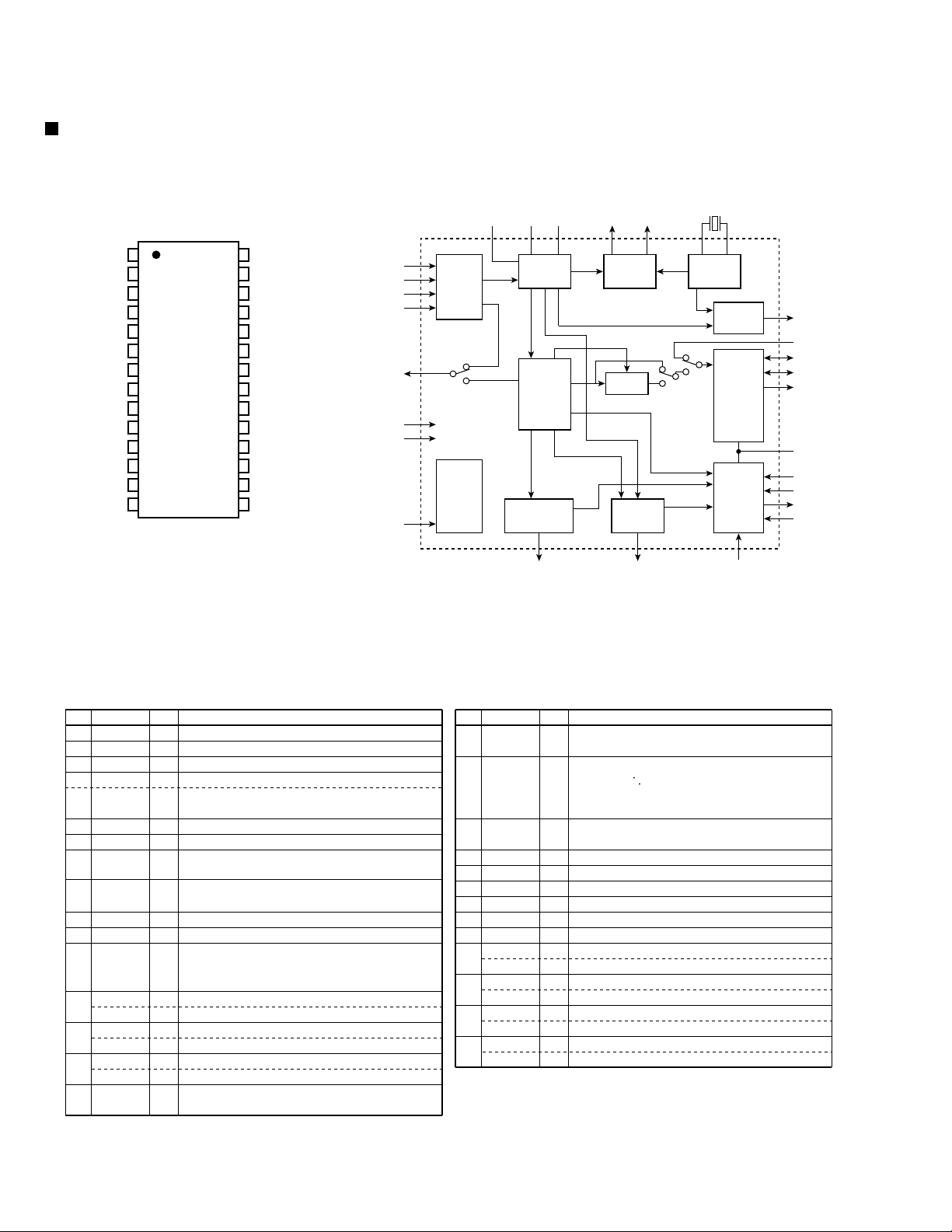
Description of major ICs
AK4112A (IC551) : 96kHz 24bit DIR
1. Pin Layout
1DVDD
2DVSS
3TVDD
4V/TX
5XTI
6XTO
7PDN
8R
9AVDD
10AVSS
11RX1
12RX2/DEF0
13RX3/DEF1
14
To p
View
28
27
26
25
24
23
22
21
20
19
18
17
16
15RX4/DEF2
CM0/CDTO
CM1/CDTI
OCKS1/CCLK
OCKS0/CSN
MCKO1
MCKO2
DAUX
BICK
SDTO
LRCK
ERF
FS96
P/SN
AUTO
2. Block diagram
RX1
RX2
RX3
RX4
V/TX
DVDD
DVSS
PDN
Input
Selector
System
Control
AVSS
AVDD R MCKO1 MCKO2 XTI XTO
Clock
Recovery
DAIF
Decoder
AC-3/MPEG
Detect
AUTO ERF P/S="L"
Clock
Generator
DEM
Error
Detect
X'tal
Oscillator
96kHz
Detect
Audio
uP I/F
FS96
DAUX
LRCK
BICK
SDTO
I/F
TVDD
CSN
CCLK
CDTO
CDTI
3. Pin Function
No.
1
2
3
4
5
6
7
8
9
10
11
12
13
14
15
Pin Name
DVDD
DVSS
TVDD
V
TX
XTI
XTO
PDN
R
AVDD
AVSS
RX1
DIF0
RX2
DIF1
RX3
DIF2
RX4
AUTO
I/O
-
-
O
O
I
O
I
-
-
-
I
I
I
I
I
I
I
O
Function
Digital Power Supply Pin, 3.3V
Digital Ground Pin
Input Buffer Power Supply Pin, 3.3V or 5V
Validity Flag Output Pin in parallel mode
Transmit channel (through data)
Output Pin in serial mode
X'tal Input Pin
X'tal Output Pin
Power-down mode Pin
When "L", the AK4112A is powerd-down and reset.
External resister pin
18Kohm +/-1% resistor to AVSS externally.
Analog Power Supply Pin
Analog Ground pin
Receiver Channel 1
This channel is selected in parallel mode
or default of serial mode.
Audio Data Interface format 0 Pin in parallel mode
Receiver Channel 2 in serial mode
Audio Data Interface format 1 Pin in parallel mode
Receiver Channel 3 in serial mode
Audio Data Interface format 2 Pin in parallel mode
Receiver Channel 4 in serial mode
Non-PCM Detect Pin
"L": No detect, "H": Detect
No.
Pin Name
16
P/S
17
FS96
18
ERF
19
LRCK
20
SDTO
21
BICK
22
DAUX
23
MCKO2
24
MCKO1
25
OCKS0
CSN
26
OCKS1
CCLK
27
CM1
CDTI
28
CM0
CDTO
Note: All input pins except internal pull-down pins should not be left floating.
Function
I/O
Palrallel/Serial Select Pin
I
"L": Serial mode, "H": Parallel mode
96kHz sampling detect pin
O
(RX mode) "H" : fs=88.2kHz or more,
"L" fs=54kHz or Iess.
(X'tal mode) "L" : XFS96=1, "L" : XFS96=0.
Unlock & Parity Error Output Pin
O
"L": No error, "H": Error
Output Channel Clock Pin
I/O
Audio Serial Data Output Pin
O
Audio Serial Data Clock Pin
I/O
Auxiliary audio data input pin
I
Master Clock #2 Output Pin
O
Master Clock #1 Output Pin
O
Output Clock Select 0 Pin in parallel mode
I
Chip Select Pin in serial mode
I
Output Clock Select 1 Pin in parallel mode
I
Control Data Clock Pin in serial mode
I
Master Clock Operation Mode Pin in parallel mode
I
Control Date Input Pin in serial mode
I
Master Clock Source select Pin in parallel mode
I
Control Date Output Pin in serial mode
O
1-12
Page 13
AK4527B (IC571) : A/D,D/A converter
1.Pin layout
LOOP1
LOOP0/SDA/CDTI
DIF1/SCL/CCLK
DIF0/CSN
P/S
MCLK
DZF1
AVSS
AVDD
VREFH
VCOM
RX-8012VSL/RX-8010VBK
SDOS
OCKS
MIS
BCLK
LRCK
SDTI1
SDTI2
SDTI3
SDTO
DAUX
DFS
2.Block diagram
LIN+
LIN-
4443424140393837363534
1
2
3
4
5
6
7
8
9
10
11
1213141516171819202122
DEM1
DEM0
MCKO
DVDD
DVSSPDXTS
ICKS1
ADC
ICKS0
HPF
CAD1
CAD0
33
32
31
30
29
28
27
26
25
24
23
DZF2
RIN+
RINLIN+
LINROUT1
LOUT1
ROUT2
LOUT2
ROUT3
LOUT3
Audio
I/F
RIN+
RIN-
LOUT1
ROUT1
LOUT2
ROUT2
LOUT3
ROUT3
HPF
DATT
DATT
DATT
DATT
DATT
DATT
LRCK
BICK
MCLK
SDOUT
SDIN1
SDIN2
SDIN3
LPF
LPF
LPF
LPF
LPF
LPF
ADC
DAC
DAC
DAC
DAC
DAC
DAC
Block Diagram (DIR and AC-3) DSP are external parts)
DAUX
Format
Converter
SDOS
SDTO
SDTI1
SDTI2
SDTI3
1-13
Page 14

RX-8012VSL/RX-8010VBK
3. Pin function (1/2)
No.
1
2
3
4
5
6
7
8
9
10
11
12
13
14
15
16
17
18
19
20
21
22
23
24
25
26
27
28
29
30
31
32
Pin name
SDOS
OCKS
MIS
BICK
LRCK
SDTI1
SDTI2
SDTI3
SDTO
DAUX
DFS
DEM1
DEM0
MCKO
DVDD
DVSS
PD
XTS
ICKS1
ICKS0
CAD1
CAD0
LOUT3
ROUT3
LOUT2
ROUT2
LOUT1
ROUT1
LINLIN+
RINRIN+
I/O
SDTO Source select pin
I
"L" : Internal ADC output, "H" : DAUX input
ORed with serial control register if P/S="L".
MCKO Clock frequency select pin
I
"L" : MCLK, "H" : MCLK/2. ORed with serial control register if P/S= "L".
Connect to GND
I
Audio serial data clock pin
I
Input/Output channel clock pin
I/O
DAC1 Audio serial data input pin
I
DAC2 Audio serial data input pin
I
DAC3 Audio serial data input pin
I
Audio serial data output pin
O
AUX Audio serial data input pin
I
Double speed sampling mode pin
I
"L" : Normal speed, "H" : Double speed, the ADC is powered down.
ORed with serial control register if P/S="L".
De-emphasis pin
I
ORed with serial control register if P/S="L"
De-emphasis Pin
I
ORed with serial control register if P/S="L"
Master clock output pin
O
Digital power supply pin
Digital ground pin
Power-down & Reset pin
I
When "L", the AK4527 is powered-down and the control registers are reset
to default state. If the state of CAD0-1 changes, then the AK4527
must be reset by PDN.
X'tal oscillator Select/Test mode pin
I
"H" : X'tal Oscillator selected
"L" : External clock source selected
Input clock select 1 pin
I
Input clock select 0 pin
I
Chip address pin
I
Used during the serial control mode.
Chip address pin
I
Used during the serial control mode.
Lch #3 analog output pin
O
Rch #3 analog output pin
O
Lch #2 analog output pin
O
Rch #2 analog output pin
O
Lch #2 analog output pin
O
Rch #1 analog output pin
O
Lch analog negative Input Pin
I
Lch analog positive Input Pin
I
Rch analog negative Input Pin
I
Rch analog positive Input Pin
I
Function
AK4527(1/2)
1-14
Page 15
RX-8012VSL/RX-8010VBK
3.Pin function (2/2)
No.
33
34
35
36
37
38
39
40
41
42
43
44
Pin Name
DZF2
VCOM
VREFH
AVDD
AVSS
XTI
XTO
MCKI
P/S
DIF0
CS
DIF1
CCLK
LOOP0
CDTI
LOOP1
CDTO
I/O
O
O
I
-
I
O
I
I
I
I
I
I
I
I
I
O
AK4527(2/2)
Function
Zero Input detection pin, 2PIN
Common voltage output pin,AVDD/2
Large external capacitor around 2.2uF is used to reduce power-supply noise
Positive voltage reference input pin,AVDD
Analog power supply pin
Analog ground pin
X'tal input pin
X'tal output pin if XTS="H"
External master clock input pin if XTS="L"
Parallel/Serial select pin
"L" : Serial control mode, "H" : Parallel control mode
Audio data interface format pin in parallel mode
Chip select pin in serial mode
Audio data interface format pin in parallel mode
Control data clock pin in serial mode
Loop back mode pin in parallel mode
Enables digital loop-back from ADC to 3 DACs.
Control data input pin in serial mode
Loop back mode pin in parallel mode
Enable all 3 DAC channels to be input from SDTII.
Control data output pin in serial mode
1-15
Page 16
RX-8012VSL/RX-8010VBK
BA15218F (IC303, IC304, IC372, IC385, IC386, IC521, IC522, IC523, IC524, IC525, IC526,
IC527, IC528, IC529) : Op amp.
1OUT1
2-IN1
-
8
7
V
CC
OUT2
1
3+IN1
+
-
-IN2
6
2
EE
4
+
5V
+IN2
BA7625 (IC201, IC242) : Video selector
MONITOR OUT
GND
IN5
GND
IN4
CTL E
IN3
CTL D
1
2
3
4
5
6
7
8
logic
logic
16
15
14
13
12
11
10
11
IN1
CTL A
VOUT 1
CC
V
IN2
CTL B
VOUT 2
CTL C
A B E MONITOR OUT
LL
HL
LH
H H L IN4
H H H IN5
*
*
*
IN1
IN2
IN3
C D E VOUT1
LL
HL
LH
H H L IN4
H H H IN5
*
*
*
-IN2
IN3
C D E VOUT2
LL
HL
LH
H H L IN4
H H H IN5
*
*
*
IN1
-IN3
BA7626 (IC241) : Video selector
MONITOR OUT
GND
IN5
GND
IN4
CTL E
IN3
CTL D
1
2
3
4
5
6
7
8
logic
logic
1-16
16
15
14
13
12
11
10
11
IN1
CTL A
VOUT 1
V
CC
IN2
CTL B
VOUT 2
CTL C
A B E MONITOR OUT
LL
HL
LH
H H L IN4
H H H IN5
*
*
*
IN1
IN2
IN3
C D E VOUT1
LL
HL
LH
H H L IN4
H H H IN5
*
*
*
-IN2
IN3
C D E VOUT2
LL
HL
LH
H H L IN4
H H H IN5
*
*
*
IN1
--
IN3
Page 17
BU2092(IC402) : Port expander
1.Terminal Layout
RX-8012VSL/RX-8010VBK
Vss
DATA
CLOCK
LCK
Q0
Q1
Q2
Q3
Q4
1
2
3
4
5
6
7
8
9
CONTROL
CIRCUIT
12BIT SHIFT RESISTER
12BIT STRAGE RESISTER
OUTPUT BUFFER(OPEN DRAIN)
17
16
15
14
13
12
11
10
18
Vdd
OE
Q11
Q10
Q9
Q8
Q7
Q6
Q5
2.Pin Function
Pin No.
1
2
3
4
5~16
17
18
Symbol
Vss
DATA
CLOCK
LCK
Q0~Q11
OE
Vdd
I/O
I
I
I
O
I
-
Function
Connect to GND
Serial Data input
Shift Clock of Data
Latch Clock of Data
Parallel Data Output
Latch Data L H
OUTPUT ON OFF
Output Enable
Power Supply
1-17
Page 18
RX-8012VSL/RX-8010VBK
MB90088 (IC203) : On screen display controller
1.Terminal Layout
YIN
VIN
CIN
AVcc
IOUT
VOC
Vcc
EXS
XS
HSYNC
VSYNC
EXHSYN
EXVSYN
Vss
2.Block Diagram
SIN
SCLK
CS
EXHSYN
EXVSYN
1
2
3
4
5
6
7
8
9
10
11
12
13
14
28
AVss
27
YOUT
26
VOUT
25
COUT
24
CS
23
SIN
22
SCLK
21
TEST
20
BOUT
19
ROUT
18
GOUT
17
VOB
16
XD
15
EXD
Serial Input
Control
H/V Separate
Each Control, Data
VIN
YIN
CIN
HSYNC
VSYNC
XS
EXS
XD
EXD
NTSC/PAL
Signal OSC
Display Memory
Control
VRAM
4FSC CLK
OSC
Dot CLK
OSC
Each Block
Each Block
Analog SW
Video Signal
OSC
Output
Control
CGROM
VOUT
YOUT
COUT
BOUT
ROUT
GOUT
IOUT
VOC
VOB
1-18
Page 19
3.Functions
pin
Symbol I/O Function
no
YIN
1
2
3
4
5
6
7
8
9
10
11
12
13
14
15
16
17
18
19
20
21
22
23
24
25
26
27
28
VIN
CIN
AVcc
IOUT
VOC
Vcc
EXS
XS
HSYNC
VSYNC
EXHSYN
EXVSYN
Vss
EXD
XD
VOB
GOUT
ROUT
BOUT
TEST
SCLK
SIN
CS
COUT
VOUT
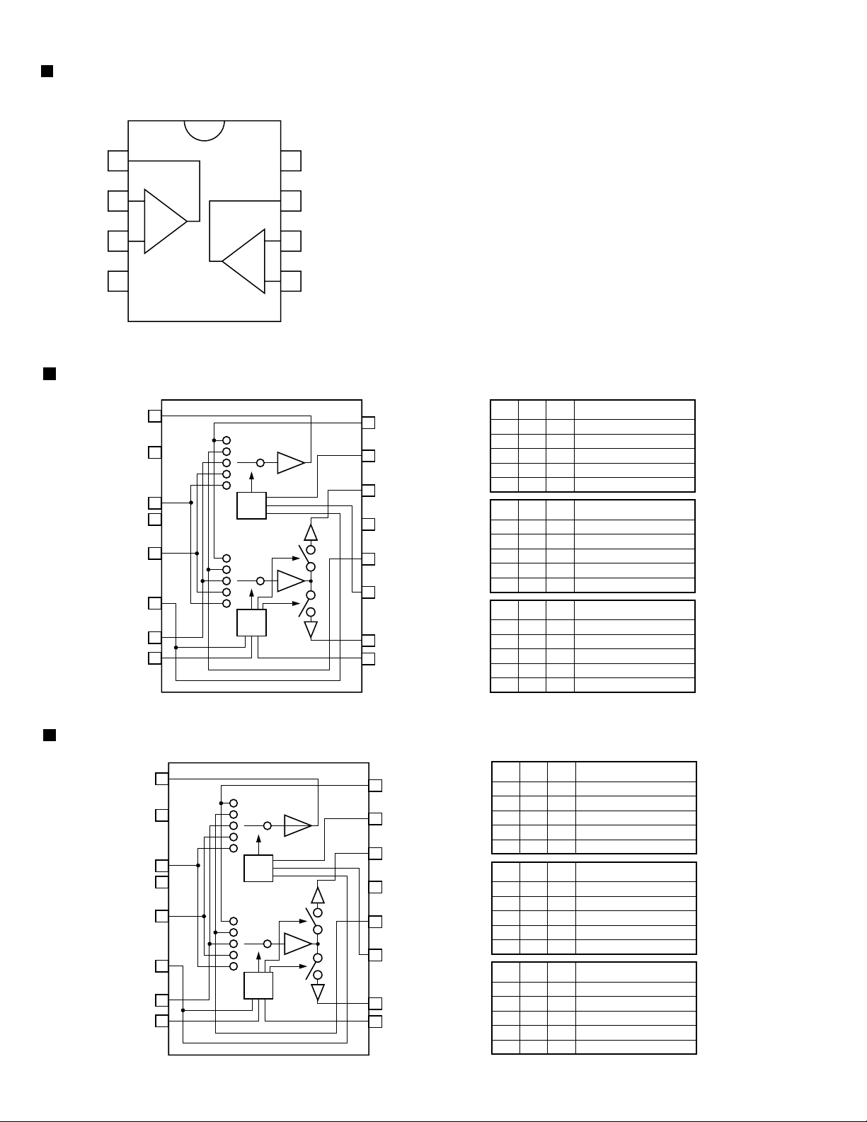
YOUT
AVs s
I
Lux signal Input terminal for Superinpause indication
I
Composite video signal input terminal for Superinpause indication
Contrast signal input terminal for Superinpause indication
I
-
Analog power supply terminal
O
Color (Lux) signal output terminal
Character output terminal
O
Power supply terminal
Clock generater outside circuit terminal for color burst
I
O
O
Horizontal signal output terminal
O
Vertical signal output terminal
EXT horizontal signal input terminal
I
EXT vertical signal input terminal
I
GND
-
Dot clock generater outside circuit signal terminal for indication
I
O
Character & background signal output terminal
O
Color signal (Green, Red, Blue)
O
I
Test signal input terminal
Shift clock input terminal for serial transmission
I
Serial data input terminal
I
Chip select terminal
I
Contrast signal output terminal
O
Composite video signal output terminal
O
Lux signal output terminal
O
Analog GND terminal
-
RX-8012VSL/RX-8010VBK
1-19
Page 20
RX-8012VSL/RX-8010VBK
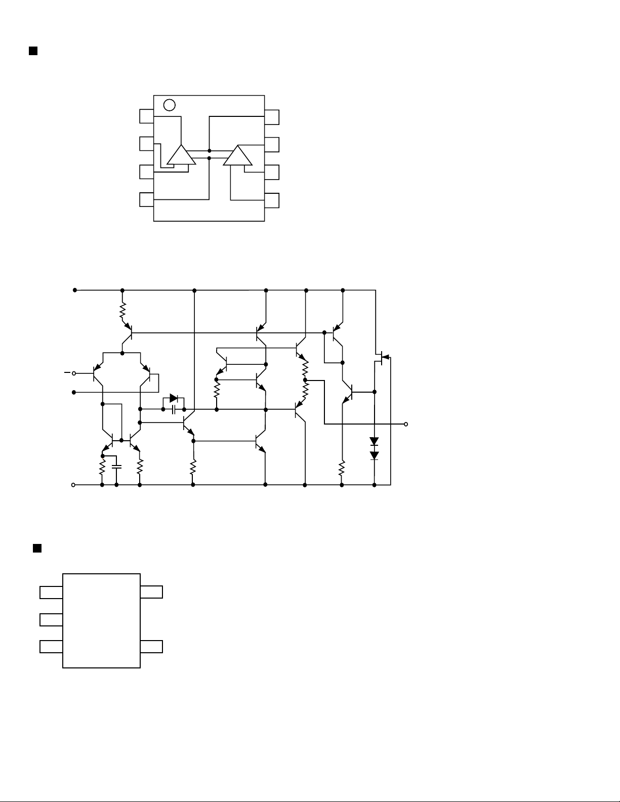
NJM4580D (IC301) : LPF, Mic and h.phone amp.
1.Terminal layout
2.Block diagram
+
V
INPUT
+
A OUT
A -IN
A +IN
V
1
2
A
3
-
4
(TOP VIEW)
B
8
7
6
5
+
V
B OUT
B -IN
B +IN
-
V
NJU7241F33(IC411) : Voltage regulator
PIN FUNCTION
1
5
2
3
4
1. GND
2. VIN
3. VOUT
4. +NC
5. STB
OUTPUT
1-20
Page 21
PCM2702E-X (IC410) : Digital/ Analog converter
RX-8012VSL/RX-8010VBK
1.Pin layout
XTI
1
DD
C
V
2
DGNDC
3
DD
V
4
DGND
5
D+
6
D-
7
BUS
V
8
DGND
9
PLYBCK
10
SSPND
11
ZERO
12
TEST3
13
TEST2
14
3.Pin function
XTO
VccP
AGNDP
VccL
AGNDL
OUT
V
Vcc
COM
V
AGND
OUT
V
AGNDR
VccR
TEST0
TEST1
2. Block diagram
PLYBCK
28
27
26
25
24
L
23
22
21
20
R
19
18
17
16
15
D+
D-
VBUS
DGNDU
VDDC
DGNDC
SSPDN
USB I/F
MCLK
USB clock
generator
Crystal OSC
XTI
XTO
USB packet
data
WRCLK
FIFO
SPACT
audio
data
RDCLK
ZERO
8x
Oversampling
Digital Filter
System Clock
Audio clock
generator
DGNDP
VDDP
Multi-level
Delta-Sigma
Modulator
VccL
AGNDL
VccR
AGNDR
DAC
DAC
Power supply
VCC AGND VDD DGND
Low-pass
Filter
Low-pass
Filter
VOUTL
VCOM
VOUTR
PIN
1
2
3
4
5
6
7
8
9
10
11
12
13
14
15
16
17
18
19
20
21
22
23
24
25
26
27
28
Symbol
XTI
DD
C
V
DGNDC
DD
V
DGND
D+
D-
BUS
V
DGNDU
PLYBCK
SSPND
ZERO
TEST3
TEST2
TEST1
TEST0
VccR
AGNDR
OUT
R
V
AGND
COM
V
Vcc
OUT
L
V
AGNDL
VccL
AGNDP
VccP
XTO
I/O
IN
-
-
-
I/O
I/O
IN
-
OUT
OUT
OUT
IN
IN
IN
IN
-
-
OUT
-
-
-
OUT
-
-
-
-
OUT
Function
Crystal Oscillator Input.
Digital Power Supply for Clock Generator, +3.3V.
Digital Ground for Clock Generator.
Digital Power Supply, +3.3V.
Digital Ground.
USB Differential Input/Output Plus.
USB Differential Input/Output Minus.
USB Bus Power (This pin NEVER consumes the USB bus power).
Digital Ground for USB Transceiver.
Playback flag, active LOW. (LOW: playback, HIGH: idle).
Suspend flag, active LOW. (LOW: suspend, HIGH: operational).
Zero flag, (LOW: Normal, HIGH: ZERO).
Test pin 3. Connect to digital ground.
Test pin 2. Connect to digital ground.
Test pin 1. Connect to digital ground.
Test pin 0. Connect to digital ground.
Analog Supply for R-channel, +5V.
Analog Ground for R-channel.
Analog Output for R-channel.
Analog Ground.
Common for DAC.
Analog Supply, +5V.
Analog output for L-channel.
Analog Ground for L-channel.
Analog Supply for L-channel, +5V.
Analog Ground for PLL.
Analog Supply for PLL, +5V.
Crystal Oscillator Output.
(1)
(2)
(2)
(2)
(2)
(2)
Note:
(1) 3.3V tolerant.
(2) Schmitt trigger input with internal pull-down, 5V tolerant.
1-21
Page 22
RX-8012VSL/RX-8010VBK
TC9162AN (IC380) : Analog switch
VSS
L-S1
L-S2
L-COM1
L-S3
L-S4
L-COM2
L-S5
L-S6
L-COM3
L-S7
L-COM4
ST
GND
L-S1
1
2
3
4
5
6
7
8
9
10
11
12
13
14
2
28
27
26
25
24
23
22
21
20
19
18
17
16
15
VDD
R-S1
R-S2
R-COM1
R-S3
R-S4
R-COM2
R-S5
R-S6
R-COM3
R-S7
R-COM4
DATA
CK
VSS
GND VDD
1
14
28
27
R-S1
L-S2
L-COM1
L-S3
L-S4
L-COM2
L-S5
L-S6
L-COM3
L-S7
L-COM4
ST
3
4
5
6
7
8
9
10
11
12
13
LEVEL SHIFTER
LATCH CIRCUIT
LATCH CIRCUIT
LEVEL SHIFTER
26
25
24
23
22
21
20
19
18
17
16
R-S2
R-COM1
R-S3
R-S4
R-COM2
R-S5
R-S6
R-COM3
R-S7
R-COM4
DATA
1-22
SHIFT REGISTER
15
CK
Page 23
TC9163AF-X (IC371) : Analog switch
RX-8012VSL/RX-8010VBK
VSS
L-S1
L-S2
L-S3
L-COM1
L-S4
L-S5
L-S6
L-COM2
L-S7
L-S8
L-COM3
ST
GND
L-S1
L-S2
1
2
3
4
5
6
7
8
9
10
11
12
13
14
2
3
28
27
26
25
24
23
22
21
20
19
18
17
16
15
VDD
R-S1
R-S2
R-S3
R-COM1
R-S4
R-S5
R-S6
R-COM2
R-S7
R-S8
R-COM3
DATA
CK
VSS
GND VDD
1
14
28
27
26
R-S1
R-S2
L-S3
L-COM1
L-S4
L-S5
L-S6
L-COM2
L-S7
L-S8
L-COM3
ST
10
11
12
13
4
5
6
7
8
9
LEVEL SHIFTER
LATCH CIRCUIT
LATCH CIRCUIT
LEVEL SHIFTER
SHIFT REGISTER
25
24
23
22
21
20
19
18
17
16
15
R-S3
R-COM1
R-S4
R-S5
R-S6
R-COM2
R-S7
R-S8
R-COM3
DATA
CK
1-23
Page 24
RX-8012VSL/RX-8010VBK
TC9164AF-X (IC302) : Analog switch
VSS
L-S1
L-S2
L-S3
L-S4
L-COM1
L-S5
L-S6
L-COM2
L-S7
L-S8
L-COM3
ST
GND
L-S1
L-S2
1
2
3
4
5
6
7
8
9
10
11
12
13
14
2
3
28
27
26
25
24
23
22
21
20
19
18
17
16
15
VDD
R-S1
R-S2
R-S3
R-S4
R-COM1
R-S5
R-S6
R-COM2
R-S7
R-S8
R-COM3
DATA
CK
VSS
GND VDD
1
14
28
27
26
R-S1
R-S2
L-S3
L-S4
L-COM1
L-S5
L-S6
L-COM2
L-S7
L-S8
L-COM3
ST
4
5
6
7
8
9
10
11
12
13
LEVEL SHIFTER
LATCH CIRCUIT
SHIFT REGISTER
LATCH CIRCUIT
LEVEL SHIFTER
25
24
23
22
21
20
19
18
17
16
15
R-S3
R-S4
R-COM1
R-S5
R-S6
R-COM2
R-S7
R-S8
R-COM3
DATA
CK
1-24
Page 25
TC9459F (IC381, IC382, IC383) : Electronic volume control
RX-8012VSL/RX-8010VBK
1.Terminal layout
VSS
L-OUT
NC
L-ch
L-IN
L-LD1
L-LD2
L-A-GND
NC
CS1
NC
GND
CK
2. Block diagram
VSS
1
1
2
3
4
5
6
7
8
9
10
11
12
24
23
22
21
20
19
18
17
16
15
14
13
VDD
R-OUT
NC
R-IN
R-LD1
R-LD2
R-A-GND
NC
CS2
NC
STB
DATA
R-ch
L-OUT
NC
L-1N
L-LD1
L-LD2
L-A-GND
NC
CS1
NC
GND
CK
2
3
4
5
6
7
8
9
10
11
12
50k /
915TEP
VR
L-ch 7 to 91
decoder
L-ch data
latch circuit
Shift register (24BIT)
Level shift circuit
VDD
24
R-ch 7 to 91
decoder
R-ch data
latch circuit
Same as L-ch
Circuit
23
22
21
20
19
18
17
16
15
14
13
R-OUT
NC
R-IN
R-LD1
R-LD2
R-A-GND
NC
CS2
NC
STB
DATA
3.Pin function
Pin No.
1
2
3
4
5
6
7
8
9
10
11
12
Symbol
VSS
L-OUT
NC
NC
L-LD1
L-LD2
L-A-GND
NC
CS1
NC
NC
CK
Function
Negative power supply pin
Volume output pin
No connection
No connection
Loudness tap output pin
Loudness tap output pin
Analog GND pin
No connection
Chip select input pin
No connection
No connection
Clock input pin
Pin No.
13
14
15
16
17
18
19
20
21
22
23
24
Symbol
DATA
STB
NC
CS2
NC
R-A-GND
R-LD2
R-LD1
R-IN
NC
R-OUT
VDD
Function
Data input pin
Strobe input pin
No connection
Chip select input pin
No connection
Analog GND pin
Loudness tap output pin
Loudness tap output pin
Volume input pin
No connection
Volume output pin
Positive power supply pin
1-25
Page 26
RX-8012VSL/RX-8010VBK
MAX4018ESD (IC390) : Op amp.
ENA
ENC
ENB
Vcc
INA+
INA-
OUTA
N.C.
1
2
3
4
5
6
7
8
16
15
14
13
12
11
10
OUTC
INCINC+
V
EE
INB+
INBOUTB
N.C.
9
NJM2285V-W (IC202) : 2-input 3-channel video switch
IN1A GND1 IN2B V CTL2 IN2A GND3 IN3B
16 15 14 13 12 11 10 9
BIAS TYPE
L
+
CLAMP TYPE
H
L
CLAMP TYPE
H
H
1 2 3 4 5 6 7 8
IN1B CTL1 OUT1 GND2 OUT2 OUT3 CTL3 IN3A
L
1-26
Page 27
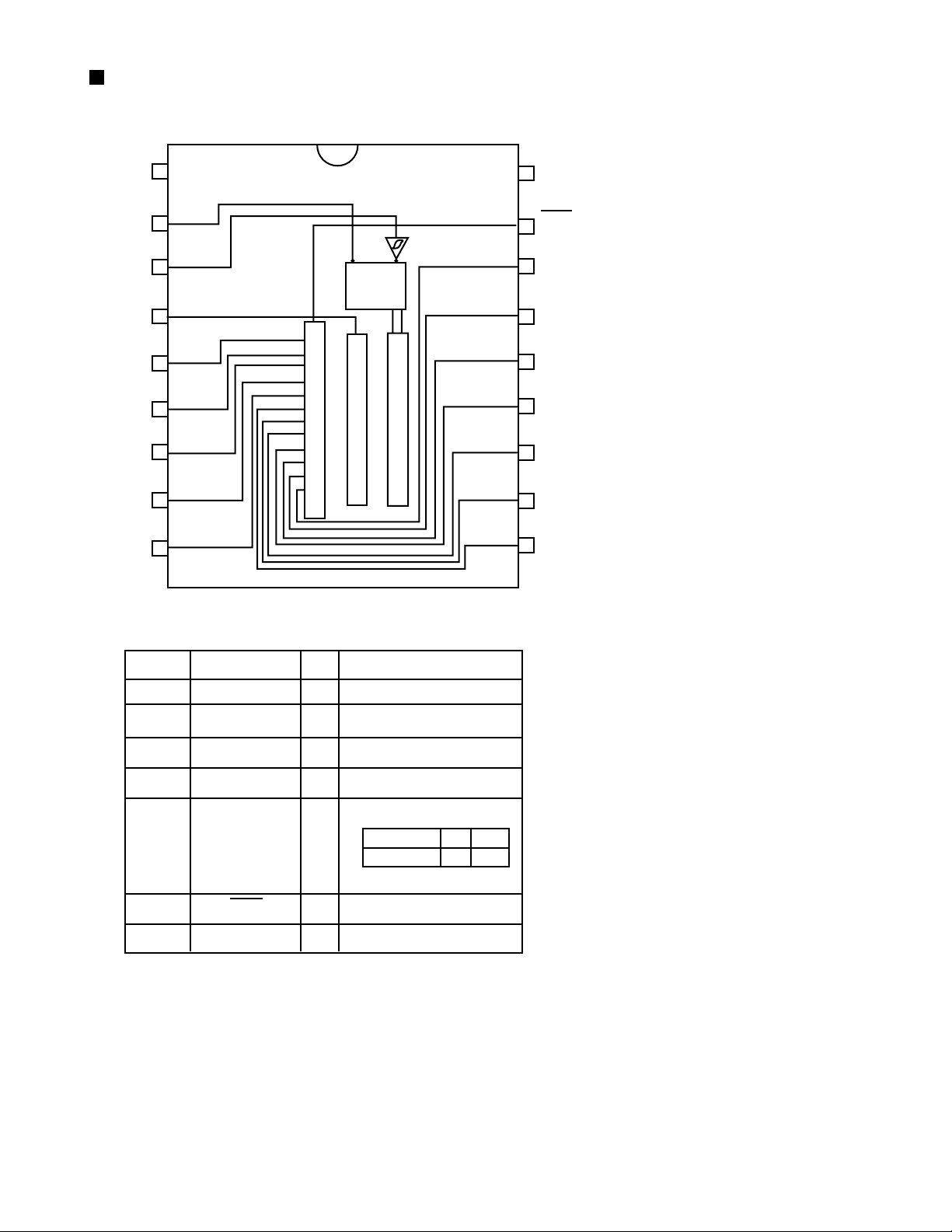
PQ3DZ53 (IC583) : Regulator IC
RX-8012VSL/RX-8010VBK
DC INPUT(Vin)
1
CUSTOM IC
5
GND
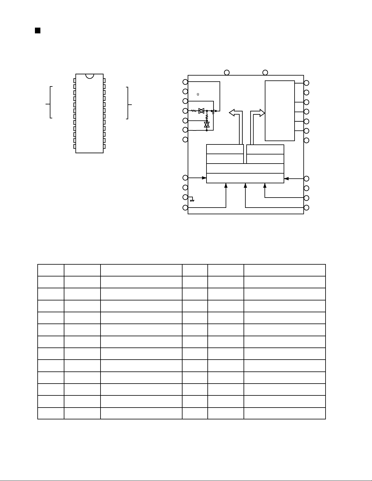
TC74HC4053AF (IC388, IC389) : Multiplexe
1Y
0Y
Z-COM
0Z
INH
EE
V
GND
1
2
IZ
3
4
5
6
7
8
16
15
14
13
12
11
10
9
Vcc
Y-COM
X-COM
1X
0X
A
B
C
CONTROL INPUTS
INHIBIT
L
L
L
L
L
L
L
L
H
X: Don't Care.
3
DC OUTPUT(Vo)
ON/OFF CONTROL(Vc)
2
C
B
A
L
L
K
L
L
H
L
H
K
L
H
H
H
L
K
H
L
H
H
H
K
H
H
H
X
X
X
W24L010AJ-12 (IC511) : CMOS static RAM
1. Pin layout
V
DD
32
A15
31
CS2
30
WE
29
A13
28
A8
27
A9
26
A11
25
OE
24
A10
23
CS1
22
I/O8
21
I/O7
20
I/O6
19
I/O5
18
I/O4
17
32
OE
31
A10
30
CS1
29
I/O8
28
I/O7
27
I/O6
26
I/O5
25
I/O4
24
Vss
23
DO3
22
DO2
21
DO1
19
A0
18
A1
17
A2
16
A3
CS2
VDD
1
NC
2
A16
3
A14
4
A12
5
A7
6
A6
7
A5
8
A4
9
A3
10
A2
11
A1
12
A0
13
I/O1
14
I/O2
15
I/O3
16
Vss
1
A11
2
A9
3
A8
4
A13
5
WE
6
7
A15
8
9
NC
10
A16
11
A14
12
A12
13
A7
14
A6
15
A5
16
A4
32-pin
TSOP
2. Block diagram
DD
V
Vss
A0
DECODER
A16
CS2
CS1
OE
WE
CONTROL
3. Pin function
SYMBOL
A0 - A16
I/O1 - I/O8
CS1, CS2
WE
OE
DD
V
Vss
NC
CORE
ARRAY
DATA I/O
I/O1
I/O8
DESCRIPTION
Address Input
Data Input/Output
Chip Select Inputs
Write Enable Input
Output Enable Input
Power Supply
Ground
No Connection
1-27
Page 28
RX-8012VSL/RX-8010VBK
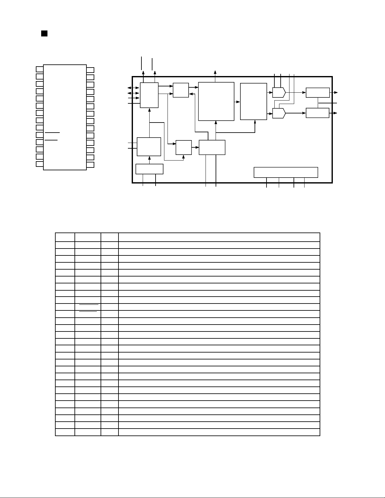
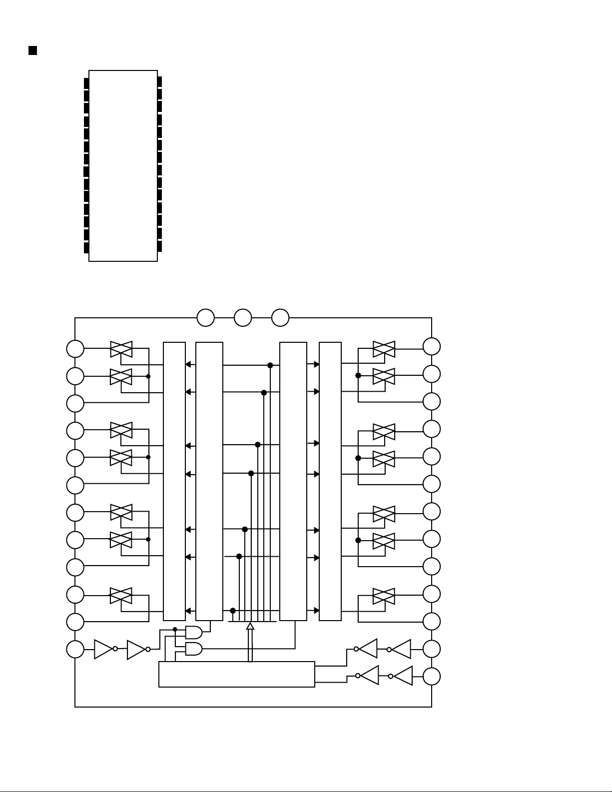
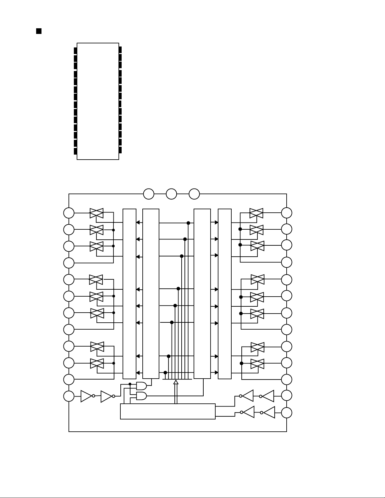
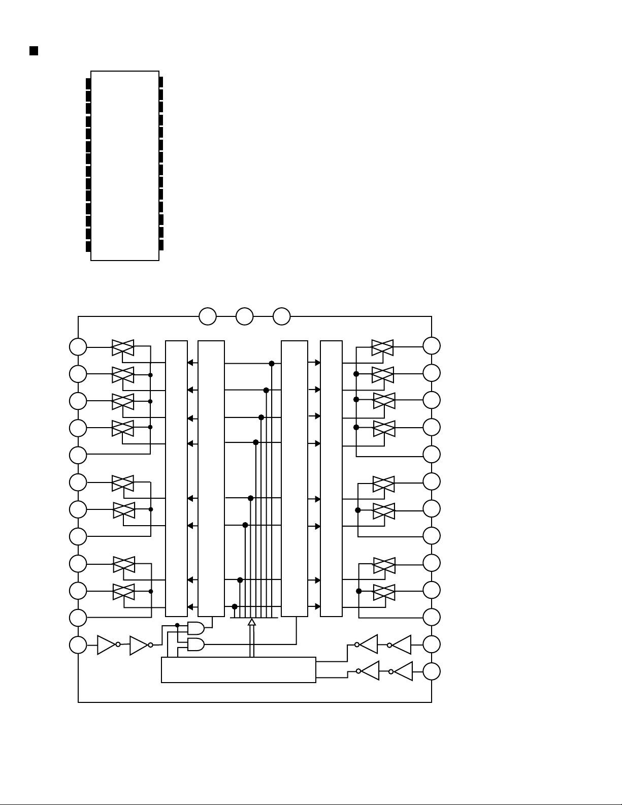
UPD784215AGC152 (IC581) : Unit CPU
1.Pin layout
75 ~ 51
76
~
50
~
100
1 ~ 25
26
2.Pin function
Pin No. Symbol I/O Function
1~8
9
10
11
12
13
14
15
16
17
18
19~22
23
24
25~32
33
34,35
36
37,38
39
40
41
42
43
44
45,46
47
48
49
50,51
52
53
54
55
56
57~63
64,65
66
67
68~70
71
72
73~75
76
77
78
79,80
81
82,83
84
85
86
87
88
89~93
94
95~100
VDD
X2
X1
VSS
XT2
XT1
RESET
AUTO
ERR
Fz96k
P03~P06
AVDD
AV REF0
P10~P17
AVSS
P130, P131
AV REF1
RX, TX
DSPCOM
DSPSTS
DSPCLK
DSPRDY
MIDIO_IN/OUT
MICK
HREQ
SS
DSP_RST
D_CS
PD/ DIR
CDTI/CDTO
CCLK
CS
PD
GND
EQ
CTR TONE
3D
VDD
ANA_TT
LEF_MIX
LEF_OUT
MIX_OUT
S_MUTE
TEST
Non connect
Power supply terminal
Connecting the crystal oscillator for system main clock
Connecting the crystal oscillator for system main clock
I
Connect to GND
Connecting the crystal oscillator for system sub clock
Connect VSS
I
System reset signal input
I
Output of DSP to general-purpose port
I
Output of DSP to general-purpose port
I
Output of DSP to general-purpose port
I
Output of DSP to general-purpose port
I
Power supply terminal
Connect to GND
Connect to GND
Connect to GND
Non connect
O
Power supply terminal
Not use
O
Non connect
O
Communication port from IC901
I
Status communication port to IC901
O
Clock input from IC901
I
Ready signal input from IC901
I
Non connect
O
Interface I/O terminal with microcomputer
I/O
Interface I/O terminal with microcomputer of clock signal
O
HREQ
I
System slave select
O
Non connect
Reset signal output of DSP
O
Non connect
Chip setselct output
O
Non connect
Reset signal output
O
Non connect
Interface I/O terminal with microcomputer
O/I
Interface I/O terminal with microcomputer of clock signal
O
CS
O
Non connect
Reset signal output
O
Connect to GND
Non connect
EQ
O
CENTER TONE
O
3D-Phonic
O
Non connect
Power supply
Non connect
Analog./T.TONE
O
Select 1
O
Select 2
O
Select 3
O
S.MUTE
O
Non connect
Test terminal
Non connect
-
1-28
Page 29

< MEMO >
RX-8012VSL/RX-8010VBK
2-29
Page 30
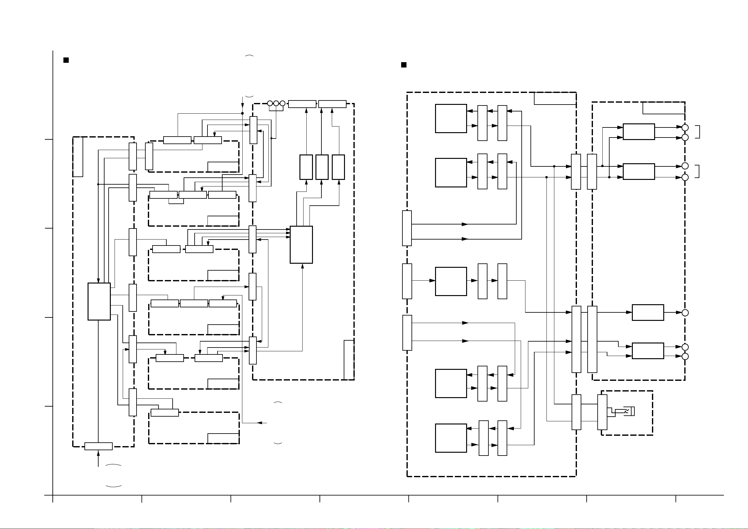
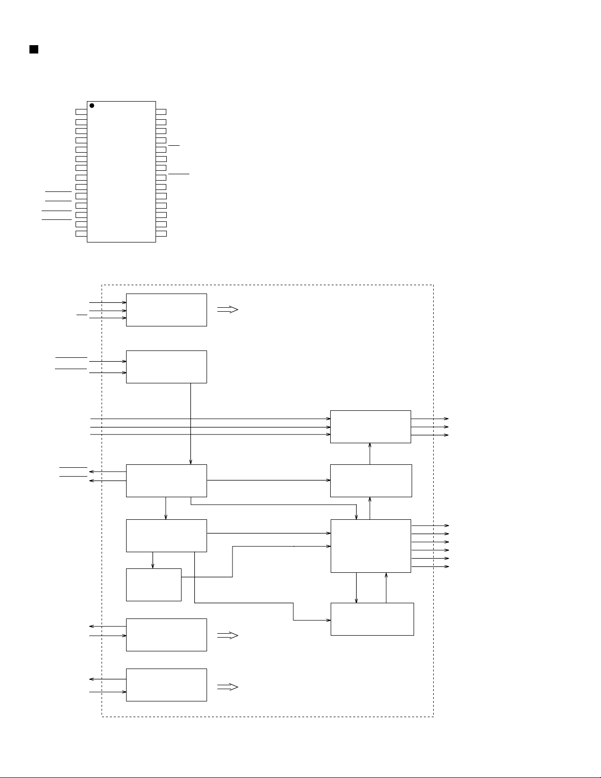
Block diagrams
Signal I/O block section
5
CN244 CN242
CN406
SYSTEM CONTROL
& FL
CN243
COMP LINK
TEXT LINK
CN731 CN732
L/R
CEN
SL/SR
Main section
L ch
Q761
Q763
CN711
CN701
LVA10221-1
RX-8012VSL/RX-8010VBK
LVA10221-2
RY831
L
SPK1
R
CN240
LVA10222-1
LVA10219-5
4
CN200 CN204 CN206
LVA10219-4
DATA
CEN
L/R
CN587 CN581
3
CPU
IC901
CN313 CN371 CN416
SL/SR
LVA10223
CN381 CN501 CN205
MON
MON
AUDIO
IC381
L/R
SW
IC380
CEN
IC382
IC383
SL/SR
CN721
CEN
CN722
R ch
L
R
Q762
Q764
Q1751
Q1752
CN712
CN713
CN702
CEN
CN703
CN813
CN823
RY832
RY851
LVA10219-3
V SIG
DVD REAR
CN723
2
DATA
CN311 CN351
CN361
SL
SR
CN814CN881
CN824
RY852
L
SPK2
R
CENTER
REAR L
REAR R
LVA10219-1
Q1851
Q1853
CN715
CN705
CN101 CN301 CN303 CN601 CN201 CN241
CN111
LVA10219-2
RL ch
FW881
& FL
CN406
Q1852
Q1854
CN716
CN706
CN400
LVA10009
SYSTEM CONTROL
RR ch
1
CN410
SYSTEM
CONTROL
& FL
ABCD E F G
2-1
Page 31

RX-8012VSL/RX-8010VBK
Video section
IC 203
LVA10219-4
DATA
CN200CN204CN206
DVD
TV/DBS
5
R
VCR1
P
R
VCR2
P
SW
IC 201
4
MON
Y/C SEP
IC 202
V SIG
FRONT VIDEO
IN (RCA)
MON Y/C OUT
MON Y/C IN
Video input section
DVD F
TV/DBS
VCR1 REC
VCR1 P.B
VCR2 REC
VCR2 P.B
LVA10219-3
DATA/CLK
CN311
SOUTCE
SELECTOR
IC 371
V SIG
CN351
USB
CN416
FRONT AUDIO
DSP section
S Video section
LVA10223
3
LVA10219-5
DIGITAL
DATA
CN240
C
C
FRONT Y/C
Y
MON Y/C
MON Y/C
CN244
CN242
IC 241
SW
DVD
2
TV/DBS
R
VCR1
P
R
VCR2
P
MON
(C)
IC 242
SW
(Y)
Y
1
IN1
DIGITAL
IN2
DIGITAL
IN3
DIGITAL
IN4
DIGITAL
OUT
SELECTOR
IC 551
DSP
CONTROLLER
IC 581
DSP
IC 501
DATA
AD/DA
CONVERTER
IC 571
SD RAM
IC 511
CN587
R/L
C
SR/SL
CN581
2-2
HABC DE FG
Page 32

RX-8012VSL/RX-8010VBK
Tuner section
System control & FL section
LVA10009
LVA10218-1
FM
5
AM
4
Audio input section
TUNER
RF 101
MW RF & OSC
T111
AM/FM DET
IC102
PLL
IC102
DATA
TUNER
CN111
KEY
FL DISPLAY D400
SYSTEM CONTROLLER
IC 400
Y/C
VIDEO
CN410
PHONO
L/R
3
CD
L/R
TAPE
P. B
EQ
IC 301
LVA10219-2
DATA/CLK
TUNER
CN311
AUDIO
CN406
USB
SOURCE
2
TAPE
REC
CDR
P. B
CDR
REC
SELECTOR
IC 302
V SIG
AUDIO
CN351
IC 303
1
DVD
REAR
ABCD E F G
IC 304
DVD REAR
2-3
Page 33

Standard schematic diagrams
Power supply section
RX-8012VSL/RX-8010VBK
5
T2
QQT0281-004
D52
1SR35-400A
1SR35-400A
15K
PW10
PW11
PW12
PW13
PW14
PW15
PW16
D57
1SS133
R53
6.8
R52
3.3K
C1
0.0047
RY1
QSK0098-001
2SD2395/EF/
D55
MTZ12JC
C53
Q51
0.0047
R54
PW21
PW22
PW23
PW24
PW25
820
KTD863/Y/
C54
470/16
Q53
KRC105M
Q52
C55
0.0047
D56
MTZ6.2JB
F4
VS1
QSW0812-001
PW28
PW29
PW40
131
132
C62C61
0.1MY0.1MY
1SR35-400A
TH71
QAD0095-4R7
113
112
111
123
122
121
134
133
1SR35-400A
0.0047/100
D51
1SR35-400A
D53
C51
C52
470/63
F2
D54
R51
Sheet 2/11
4
Sheet 10/11
CN402
3
CN72
Sheet 3/11
2
CN82
CN71
C69
0.047MY
C68
0.047MY
R74
100K
C74
1/50
MTZ8.2JC
D75
CN811
CN55
Q74
KTC3200/GL/
CN56
FW51
Q71
KTA1046/Y/
C73
22/50
R73 D74 C72
MTZ33JC
22K
F61
F62
R61
D61
10E2-FD
D63
10E2-FD
C65 C66
3300/35 1000/35
D73
1SR35-400A
3.3k
R72
C71
100/63
22/50
8.2
1SR35-400A
D62
C63
0.1MY
C70
220/50
D71
1SR35-400A
D72
1SR35-400A
D64
PW20
PW17PW27
PW26
PW18
PW19
PW30
F1
TA1
TA2
EP51
SHEET
NUMBER
1/11
POWER SUPPLY
2/11
1
MAIN
3/11
AUDIO
4/11
AUDIO SIGNAL INPUT
5/11
VIDEO SIGNAL INPUT
6/11
AUDIO AMP (FRONT CHANNEL)
7/11
AUDIO AMP (CENTER, REAR CHANNEL)
8/11
DSP
9/11
DVD
10/11
SYSTEM CONTROL
11/11
TUNER
CIRUIT DISCRIPTION
Parts are safety assurance parts.
When replacing those parts make
sure to use the specified one.
SHEET 1/11
2-4
HABC DE FG
Page 34

Main & Speaker terminal section
RX-8012VSL/RX-8010VBK
C885
0.1
R888
R887
C835
0.022
R885
C888
0.1
C887
0.1
R833
10
10
C845
C833
220p
0.022
C834
0.022
220P 220P
C836
0.022
10
C842 C841
R834
C846
220P
C847
220P
1010
R837R838
C837
0.022
C839
C838
0.022 0.022
220P
C848
C891
220P
10
220P
C886
220P
C890
C892
220P
220P
10
C889
C893
220P
C850
4.7/50
D841
MTZ5.1JC
3.9K
R855
D845
1SS133
D846
1SS133
R867
10K
220P220P
C843C844
C881
220p
C884
220p
C883
220p
KRC109M
C840
S831
Q833
0.022
Q830
KRC109M
R865
4.7K
R858
ST831
ST851
4.7K
KRC109M
R861
Q834
4.7K
R864
4.7K
KRC109M
Q832
KRC109M
Q836
KRC109M
Q831
C852
R866
4.7K
C853
C851
4.7/504.7/504.7/50
Q835
KRC109M
D843
1SS133
D844
1SS133
D842
1SS133
R862
22K
R863
22K
22K
R859
R856
6.8K
R857
6.8K
6.8K
R860
Sheet 8/11Sheet 8/11Sheet 8/11 Sheet 7/11 Sheet 7/11Sheet 6/11 Sheet 6/11
5
CN703
CN701
CN721
CN702
CN705
CN723
CN706
RY831
RY832
R831
12
D831
1SS133
R832
12
D832
1SS133
4
CN823
CN813
R835
RY833
RY851
RY852
J91
Sheet 3/11
FW931
R852
12
R851
12
12
D835
1SS133
D851
1SS133
1SS133
D852
C816
47/25
D816
MTZ18JC
C801
D801
30DF2-FC
D803
C807C808
30DF2-FC
CN801
Sheet 1/11
C805
3
C802
D802
30DF2-FC
D804
30DF2-FC
6800/716800/71
R801R802
100K100K
2
R816
3.3k
12
R815
3.3K
R812
KTC3200/GL/
2SD2395/EF/
Q812
R811
C811
0.0047
FRONT Signal
CENTER Signal
Q811
D811
R813
0.45
L844
B124
0.45
L845
B125
0.45
L843
R841
100K
R842
82K
R843
100K
R844
100K
R845
82K
10/25
10K
R814
10k
47k
R825
C824
R826
100K
Q825
KTA1268/GL/
R824
130K
Q824
KTC3200/GL/
R823
10K
47/16
C823
Q823
KTC3199/GL/
CN831
1SS133
D825
R871
12
D871
1SS133
Sheet 3/11
RY871
QSK0109-001
CN881
FW881
R91
R92
CN824
B123
CN814
470
470
C91
C92
470P470P
Parts are safety assurance parts.
When replacing those parts make
REAR Signal
sure to use the specified one.
1
ABCD E F G
SHEET 2/11
2-5
Page 35

Audio section
EP901
R940
1.5
4.7
RX-8012VSL/RX-8010VBK
R915
8.2
R916
8.2
0.0047
D971
MTZ10JC
C972
R971
R973
12
3.3K
Q951
2SD2395/EF/
C951
100/25
D951 D961
MTZ13JC
5
2SD2395/EF/
C971
100/25
Q971
0.0047
C952
R951
R953
2.2K
12
C961
100/25
Q961
KTA1046/Y/
MTZ13JC
C962
0.0047
R963
2.2K
R961
R943
2.7K
R941
R942
33
33
C921
100/25
2SD2395/EF/
D921
MTZ5.6JC
Q921
12
2SD2395/EF/
C941
100/25
D941
MTZ5.6JC
Q941
0.0047
C942
C922
0.0047
R923
R921
2.7K
R922
33
33
C931
100/25
2SD2395/EF/
D931
MTZ6.2JC
Q931
0.0047
C932
R933
R931
R932
2.7K
R917
10
Sheet 1/11
D903
1SR35-400A
D902
1SR35-400A
D901
1SR35-400A
D900
1SR35-400A
Q908
KRC105M
CN81
4
330P
C983
330P
Q904
KRC105M
FW831
CN400
M_CLK
M_COMMAND
M_STATUS
M_CS
M_BUSY
M_RESET
STANDBY_LED
VCR_S/C
330P
C984
Q903
KRC105M
CN931
CN932
Sheet 2/11
Sheet 10/11
Sheet 2/11
CN301
10K
10K
10K
10K
4/8_OUT
10K
R966
R965
R967
VCR2_S/C
VCR1_S/C
DVD_S/C
STANDBY_LED
DSPRESET
DSPCOMMAND
DSPSTATUS
DSPCLK
R969
R968
VIDEO_S/C
DBS_S/C
DSPREADY
SW_MUTE
R944
MAIN_STB
MAIN_CLK
MAIN_DAT
SUB_STB
SUB_CLK
CN303
SUB_DAT
-15V
+15V
VOL_STB
VOL_CLK
VOL_DAT
Sheet 4/11
3
Sheet 4/11
Sheet 11/11
SUBV_STB
SUB_PRE
SUB_MUTE
S_MUTE
SW_MUTE
CN101
TUNER_DATA
TUNER_CE
TUNER_CK
TUNER_MUTE
TUNED
STEREO
R937
R938
R939
220
220
220
2
R999
RDS_ST
RDS_DATA
RDS_CLK
R936
R934
R935
10K
220
220
220
CN102
R945
R946
R947
R948
R949
R954
R955
R956
220
220
220
220
220
220
220
220
220
FL991
QQR0590-001
0.0056
FL992
QQR0590-001
C991
0.0056
C992
R975
C975
470/6.3
4.7K
4.7K
5.1K
3.3K
5.6K
R994
R996
R998
R979
C901
R977
4.7K
4.7K
6.2K
13K
D977
D978
D976
1SS133
8MHz
D979
OSD_DAT
OSD_CS
OSD_CLK
M_COMMAND
M_STATUS
M_CLK
M_RESET
M_CS
TUNED
M_BUSY
STEREO
RDS_ST
PROTECT
4/8_IN
TUNER_MUTE
TUNER_DATA
C993
100P
IC901
MN101C49GHM
TUNER_CK
TUNER_CE
RDS_DATA
RDS_CLK
D993
1SS133
D975
15K
C902
X901
R976
C903
R903
C994
270P
330
2200/6.3
C905
0.022
R978
R993
R995
R997
100/6.3
22
R991
4.7K
R992
4.7K
R908
DVD_S/C
DBS_S/C
VCR1_S/C
VCR2_S/C
CN201
VIDEO1
VIDEO2
VIDEO3
VIDEO4
OSD_CS
OSD_DAT
OSD_CLK
VIDEO5
VIDEO6
CN241
C985
0.01
IC903
IC-PST9139
R911
D904
1SS133
4.7K
Q901
KRC107M
22K
R910
C904
2.2/50
22k
220
220
220
220
220
R927
R928
R929
R925
R926
DSPCLK
DSPSTATUS
DSPREADY
DSPRESET
CN601
DSPCOMMAND
VIDEO6
S_MUTE
R924
10K
VIDEO5
SUB_MUTE
SUB_PRE
SUB_RELAY
SUR_RELAY
C_RELAY
F2_RELAY
F1_RELAY
HP_RELAY
SUBV_STB
SUB_DAT
SUB_CLK
SUB_STB
MAIN_DAT
MAIN_CLK
MAIN_STB
VOL_DAT
VOL_CLK
VOL_STB
VIDEO4
VIDEO3
VIDEO2
VIDEO1
PROTECT
HP_RELAY
F1_RELAY
F2_RELAY
SUB_RELAY
SUR_RELAY
4/8_OUT
C_RELAY
4/8_IN
R930
R980
R981
R982
R983
R984
R985
R986
R987
10K
Q907
220
220
220
220
220
220
220
220
Q906
KRC105M
330P
C981
KRC105M
C982
Q905
KRC105M
Sheet 9/11Sheet 5/11Sheet 5/11
TUNER Signal
1
Parts are safety assurance parts.
When replacing those parts make
sure to use the specified one.
SHEET 3/11
2-6
HABC DE FG
Page 36

Audio / V Audio signal input section
RX-8012VSL/RX-8010VBK
C301
R301
2.2k
4.7/50
5
C333
R333
470 470
R323
470
R325
470
R327
470
R329
470
CDR.REC-L
4
CDR.PLAY-L
R331
470
C361
4.7/50
100k100k
R361R362
R363R364
C362
4.7/50
390p
C321 C322
220p
C323 C324
220p
C325 C326
220p
C327 C328
220p
C329 C330
220p
C331 C332
220p
100k100k
BA15218F
IC304
BA15218F
IC304
C334
R334
390p
220p
R324
470
220p
R326
470
220p
R328
470
220p
R330
470
220p
R332
470
220p
C363
4.7/50
R365R366
C364
4.7/50
CDR.PLAY-R
100k100k
CD-RCD-L
REC-RREC-L
PLAY-RPLAY-L
CDR.REC-R
C302
R302
2.2k
4.7/50
J301
J302
J303
DVD-LS
DVD-RS
R305
C309C310
47k47k
100p100p
C303
R303R304
C304
100p100p
620
NJM4580DD
100/10
C314 C313
100/10
R306
620
R335
68
C335
22/25
IC302
TC9164AF-X
C336
22/25
R336
68
IC301
IC301
NJM4580DD
C305 C307
R307 R309
C306 C308
R308 R310
CD-R
CDR.PLAY-R
PLAY-R
CD-L
PLAY-L
CDR.PLAY-L
0.0018MY 0.0068MY
39k 470k
0.0018MY
39k 470k
V.SIG.R
V.SIG.L
TUNER-R
TUNER-L
0.0068MY
REC-R
REC-L
C311
4.7/50
C312
4.7/50
CDR.REC-R
CDR.REC-L
100k100k
R311R312
47/1647/16
C315C316
C339
560p
QGB1214K1-16S
CN351
R315
330
R316
330
IC303
BA15218F
V.SIG.L
V.SIG.R
DVD-LS
C1201
22/25
C1202
22/25
DVD-RS
R1201
68
IC391
TC9164AF-X
R1202
68
VOL_STB
VOL_CLK
VOL_DATA
C341
10/50
R343
100k100k
R341R342
SUB-R
CD-R
PLAY-R
CDR.PLAY-R
TUNER-RTUNER-L
R344
C342
10/50
C1209
CN311
QGB2510K1-14
TUNER-L
560p
TUNER-R
VOL_CLK
VOL_STB
VOL_DATA
CD-L
PLAY-L
CDR.PLAY-L
SUB-L
100k100k
IC303
BA15218F
C343
10/50
100k 100k
R346 R345
C344
10/50
Sheet 3/11Sheet 6/11
3
R1229
R1227
R1228
SUB-R
SUB-L
68
68
C1225
47/25
C1226
47/25
SUB.SIG.R
SUB.SIG.L
IC393
TC9459F
REAR.SIG.R
REAR.SIG.L
100k
C1227
4.7/50
C1228
4.7/50
R1230
100k
REAR.AMP.R
REAR.AMP.L
C1219
560p
C1229
4.7/50
C1230
4.7/50
C1231
220p
SUB.V.STB
SUB.DATA
SUB.CLK
R1231
SUB.MUTE
1k
IC395
BA15218F
C1243
R1245
1k
SUB.PRE
VCR1.REC-R
VCR1.REC-L
4.7/50
R1243
100k
R1244
100k
C1244
4.7/50
VCR2.REC-R
V.SIG.R
V.SIG.L
VCR2.REC-L
IC395
BA15218F
C389
560p
R371
DVD.F-L
R373
TV/DBS-L
R375
VCR1.REC-L
R377
VCR1.PLAY-L
R379
VCR2.REC-L
R381
2
VCR2.PLAY-L
R1261 R1262
C371 C372
220p 220p
C373 C374
470
220p
C375 C376
470
220p
C377 C378
470
220p
C379 C380
470
220p
C381
470
220p
C1261
470 470
220p
C391
R391
10/50
5.1k
C393
1200p
C394
1200p
C392
5.1k
10/50
220p
220p
220p
220p
C382
220p
C1262
220p
R372
470470
DVD.F-R
R374
470
J371
TV/DBS-R
R376
470
VCR1.REC-R
R378
470
J372
VCR1.PLAY-R
R380
470
VCR2.REC-R
R382
470
VCR2.PLAY-R
J373
R393
C395
10k
120p
R395
5.1k
R396R392
5.1k
C396
R394
120p
10k
IC372
BA15218F
IC372
BA15218F
C397
10/50
USB-L
R397
100k
R398
100k
USB-R
C398
10/50
2SC3576-JVC-T
Q1249 Q1247
Q1250
2SC3576-JVC-T
C385
C386
R1253
2SC3576-JVC-T
2SC3576-JVC-T
R1254 R1248
22/25
IC371
TC9163AF-X
22/25
R1247
R1249
R1251
R1252
R1250
Q1248
1k 1k
DVD.F-R
TV/DBS-R
TV/DBS-L
DVD.F-L
USB-L USB-R
1k1k
10k
10k
10k
10k
C1245
22/50
Q1245
KRA104M
VIDEO-R
VCR2.PLAY-R
VCR1.PLAY-R
VCR2.PLAY-L
VCR1.PLAY-L
VIDEO-L
R1241
100k
R1242
100k
C1241
4.7/50
C1242
4.7/50
R385
SUB-L
100k100k
R1221R1222
SUB-R
68
C1211
R386
68
C1212
C1221
10/50
C1222
R1211
68
22/25
IC392
TC9163AF-X
22/25
68
R1212
IC394
BA15218F
C1223
10/50
R1225
100k100k
R1223R1224
10/50
IC394
BA15218F
DVD.F-R
DVD.F-L
TV/DBS-R
TV/DBS-L
USB-RUSB-L
R1226
C1224
10/50
100k
100k
VCR1.PLAY-R
VCR2.PLAY-R
VCR1.PLAY-L
VCR2.PLAY-L
VIDEO-R
VIDEO-L
KRA104M
C1232
22/50
C1233
10/50
R1232
470k
Q1231
R1236
R1234
R1233
R1235
1k
10k
Q1233
2SC3576-JVC-T
10k
Q1234
2SC3576-JVC-T
1k
AUDIO Signal
TUNER Signal
PHONO Signal
VIDEO AUDIO Signal
VIDEO-R
1
VIDEO-L
Parts are safety assurance parts.
470
470
470
470
CN416
QGA2501F1-06
V.SIG.R
SUB-R
SUB-L
REAR.SIG.L
REAR.AMP.L
REAR.SIG.R
REAR.AMP.R
S.MUTE
R387
R388
R389
R390
CN371
QGB1214K1-14S
V.SIG.L
SW.MUTE
CN313
QGB2510K1-13
Sheet 6/11
SUB.CLK
SUB.DATA
SUB.MUTE
SUB.PRE
S.MUTE
SW.MUTE
SUB.V.STB
Sheet 2/11Sheet 10/11
ABCD E F G
When replacing those parts make
sure to use the specified one.
SHEET 4/11
2-7
Page 37

RX-8012VSL/RX-8010VBK
Video / S video signal input section
5
R253
CN200
QGB2510K1-11
2.2
R225
C208
47/16
C209
C201
R207
330
R200
J201
4
J202
J203
C226
47P
75
R201
75
R202
75
R203
75
R204
75
R205
75
R206
75
4.7/50
C202
R208
330
4.7/50
C203
R209
470/6.3
47k
C204
R210
330
4.7/50
C205
470/6.3
R211
47k
C206
R212
330
4.7/50
R214
C207
R213
470/6.3
47k
KTA1267/YG
KTA1267/YG
3
0.01
100
1SS133
1SS133
IC201
BA7625
MOUT
IN1
A
IN5
VOUT1
IN4
IN2
VOUT2
IN3
D
150
150
R215
Q200
Q201
R216
300
Q202
KRC110M
KRC107M
10k
R217
Q203
R219
D200
D201
Q204
KTA1267/YG
C210
4.7/50
330
R218
R220
Q205
150
KTA1267/YG
C211
4.7/50
C212
150
47
R232
R221
Q206
KTA1267/YG
Q208
DTC123YSA
IC202
NJM2285V-W
IN1B
OUT1
OUT2
OUT3
CTL3
IN3A
47/16
C213
0.01
IN2B
IN3B
C219
15p
X200
C220
10p
R231
2.2k
C231
4.7/50
Q207
KTA1267/YG
4.7/50
C215
C214
4.7/50
0.047
C216
C217
C218
1.547p
470/10
MB90088
IC203
YOUT
VOUT
COUT
CS
SIN
SCLK
XD
EXD
L200
22u
C221
560
560
560
R222
R223
R224
27p
0.001
270p
120p
C223
C224
C225
C222
OSDCS
OSDDATA
OSDCLK
Sheet 3/11
J241
C269
47P
J242
C268
47P
C276
47P
J243
C275
47P
C271
100P
R268
C270
100P
R240
75
R241
75
C242
4.7/50
R242
75
R243
75
C245
4.7/50
C246
R244
75
0.047
47k
R267
R266
C247
470/6.3
75
R245
75
75
R246
4.7/50
C250
R272
C273
75
0.047
47k
R273
R274
C274
470/6.3
75
R275
75
R276
75
C277
4.7/50
C251
R247
75
0.047
R269
47k
C252
470/6.3
75
15k
R254
15k
R255
15k
C241
0.047
150
150
R250
C244
0.047
C249
0.047
C272
0.047
4.7/50
C254
0.047
C255
KTA1267/YG
KTA1267/YG
R248
Q240
Q242
KTA1267/YG
BA7626
IC241
BA7625
IC242
150
R251
R249
Q241
R280
150
R281
Q243
KTA1267/YG
0.01
C256
300
300
R284
C258
300
300
R285
Q245
KRC110M
10k
R282
Q244
KRC107M
Q246
KRC110M
D240
C257
47/16
0.01
C259
47/16
4.7/50
0.047
10k
R283
C260
C261
Q247
KRC107M
1SS133
D241
1SS133
R271
3.3
QGB2510K1-12
CN240
Sheet 3/11
C253
10p
CN206
VIDEO
QGA2501F1-02
Sheet 10/11 Sheet 10/11
Sheet 6/11 Sheet 6/11
CN204
VIDEOY
VIDE0C
CN244
QGA2501F1-04
CN242
QGB1214K1-10SQGB1214K1-08S
2
Parts are safety assurance parts.
When replacing those parts make
sure to use the specified one.
1
2-8
SHEET 5/11
HABC DE FG
Page 38

DVD section
RX-8012VSL/RX-8010VBK
DCS
AV_VCR
TEXT
R1370
C1352
100/10
CN480
QJK017-031301
5
4
Sheet 5/11
Sheet 5/11
3
Sheet 9/11
Sheet 4/11
FW481
QUM134-10DGZ4
CN243
QGB1214J1-10S
Yin
Cin
Cmoni
Ymoni
AV_VCR
DCS
TEXT
CN205
QGB1214J1-08S
Yin
YOSD
Cin
Cmoni
Ymoni
VIDEO5
VIDEO6
CN501
QGB1214J1-12S
DSP_IN_L
DSP_IN_R
DSP.L
DSP.R
DSP.LS
DSP.RS
DSP.C
DSP.SW
CN381
QGB1214J1-14S
V.SIG.L
V.SIG.R
SUB-L
SUB-R
REAR.SIG.L
REAR.SIG.R
REAR.AMP.L
REAR.AMP.R
S.MUTE
C1354
100/10V
Q1391
KRA107M
D1392D1391
1SS1331SS133
R1391
R1398
R1393 R1396
R1395
100k 10k
100k
C1353
R1392
39k
R1394
C1351
39k
27k
1000p
1k
Q1392
KTA1273/Y/-T
R1399
1.5k
IC387
NJM2406F-X
R1397
5.6
0.1u
J1390
C1301
47/25
C1302
47/25
IC380
TC9162AN
J1370
J1371
J1372
68
R1301
DSP.R
FRONT-RFRONT-L
68
R1302
DSP.L
DVD-LS DVD-RS
DSP.RS
DSP.LS
DVD-SW
DVD-C
C1371
R1375
DSP.C DSP.SW
470
220
R1371
R1372
100
220p
R1373
220
220p 220p
C1372 C1370
R1374
220
220
D1370
MA3062/H/-X
C1305
R1305
68
1.2k
DSP_IN_R
R1304
CLK
STB DATA
C1303
1.2k
220p
R1303
DSP_IN_L
R1306
68
47/25
C1306
2
CN361
QGB1214J1-16S
V.SIG.L
V.SIG.R
SUB-L
SUB-R
FRONT-L
FRONT-R
DVD-LS
DVD-RS
STB
CLK
Sheet 4/11
1
DATA
VOL_STB
VOL_CLK
VOL_DATA
J1360
DSP_IN_L
R1355
2.2k
FRONT-L
R1357
3.9k
R1358
3.9k
FRONT-R
R1356
DSP_IN_R
2.2k
R1361
C1363
560
4.7/50
R1363R1364
C1361
100k100k
C1362
C1364
R1362
560
4.7/50
IC386
BA15218F
C1365
DVD-C
IC386
BA15218F
4.7/50
100k100k
R1367R1368
C1366
DVD-SW
4.7/50
R1365
100k
R1366
100k
J1340
Q1343
390P
C1345
KRA104M
R1347
470
R1348
470k
10k
Q1342
R1349
2SC3576-JVC-T
Q1341
2SC3576-JVC-T
R1351
68
IC385
BA15218F
R1350
68
BA15218F
C1342
R1345
470
4.7/50
R1344
100k
R1346
10k
47/25
C1344
C1343
47/25
4.7/50
IC385
R1343
18k
C1341
R1341
100k
1k
R1342
YOSD
1.6k4.7k
R1293R1294
0.01
47/25
TC74HC4053AF
C1375
C1376
IC388
R1312
100k
C1312
4.7/50
4.7/50
IC381
TC9459F
47/25
4.7/50
4.7/50
C1311
C1313 C1314
100k
R1311
R1322
100k
4.7/50
C1324C1323
4.7/50
C1322
IC382
TC9459F
C1321
4.7/50
4.7/50
R1321
100k
R1332
100k
C1334
4.7/50
4.7/50
C1332C1331
IC383
TC9459F
4.7/50
4.7/50
C1333
R1331
100k
VIDEO6
VIDEO5
C1380
47/25
C1316
220p
C1319
0.22/50
VOL_STB
VOL_DATA
VOL_CLK
C1315
0.22/50
C1329
220p
C1326
0.22/500.22/50
VOL_STB
VOL_DATA
VOL_CLK
C1325
C1339
220p
VOL_STB
VOL_DATA
VOL_CLK
Parts are safety assurance parts.
When replacing those parts make
sure to use the specified one.
C1381 C1382 C1383
47P 47P 47P
R1379
75
C1384 C1385 C1386
Q1307
KRA104M
R1385
100k100k
R1337R1338
47/25 4.7/50 4.7/50
C1387 C1388 C1389
47P 47P 47P
R1382
75
C1390 C1391 C1392
47/25 4.7/50 4.7/50
C1393 C1394 C1395
100P 100P 100P
75
R1386
R1388
47k
C1396 C1397
470/6.3 100/10
IC384
BA15218F
C1337
10/50
C1338
10/50
IC384
BA15218F
0.01
47/25
TC74HC4053AF
C1377
C1378
IC389
R1281
4.7k
C1281
100/10
C1283
47/25
C1285
47/25
S.MUTE
CCH
R1282
4.7k
R1285
4.7k
R1286
4.7k
R1289
4.7k
R1290
4.7k
R1323
1k
R1324
10k
R1333
1k
R1335
10k
2SC3576-JVC-T
R1334
10k
2SC3576-JVC-T
R1336
1k
IC390
MAX4018ESD
R1284
1.1k
R1283
1k
C1282
470/10
IC390
MAX4018ESD
R1288
1.1k
R1287
1k
C1284
100/10
IC390
MAX4018ESD
R1292
1.1k
R1291
1k
C1286
100/10
C1307
R1307
47/16
1k
Q1323
2SC3576-JVC-T
C1335
10/50
Q1333
Q1334
C1336
10/50
R1381R1380
7575
J1380
R1384R1383
7575
75
75
R1387
R1390
R1389
R1339R1340
47k
47k
C1398
100/10
R1313
1k
R1315
10k
Q1313
2SC3576-JVC-T
R1314
10k
Q1314
2SC3576-JVC-T
R1316
1k
REAR.SIG.L
100k100k
REAR.SIG.R
0
0
R1329
R1330
REAR.AMP.L
REAR.AMP.R
CN731
QJP001-032301
SIG.L
SIG.R
Sheet 2/11
CN732
WJP0026-001A
SIG.C
Sheet 2/11
AUDIO Signal
FRONT Signal
CENTER Signal
REAR Signal
ABCD E F G
SHEET 6/11
2-9
Page 39

RX-8012VSL/RX-8010VBK
Audio amplifier section (1/2)
C751
47P
D771
1SS133
KTC3200/GL/
KTA1268/GL/
D773
1SS133
R775
R777
R761
10
R771
390
200
200
R773
390
R763
10
C753
47P
Q761
Q763
R779
0.22( 7W)
R795
R787
R791
47K
33
L791
1
R793
10
C791
0.047
C793
0.047
Q791
KTA1268/GL/
C795
0.022
1K
15K
R797
D791
1SS133
R707R705
2K
2K
150
R721
Q707
KTA1268/GL
1.5K
R725
R733
C711
Q705
KTA1268/GL/
0.01
220
5.6K
R717
C717
22P( 500V)
10K
R719
390
R723
390
D703
1SS133
R731
33K
R727
C713
C715
KTA1268/GL/
Q709
68P
68P
390
R729
Q711
KTC3200/GL/
C709
620
R715
R711
C707
100/16
10P
100K
C741
47/100
C719
0.0047MY
VR787
500
R783
620
Q781
2SD637( Q.R)
R781
390
5
D701
1SS133
R701 C701
10/35
2.2K
C703 R703
100P
100K
C705
100P
Q701
2SC2240-BL/AB
Q703
2SC2240-BL/AB
R709
9.1K
R789
470
TH783
QAD0012-202
Q771
Q773
4
C745
47/100
CN711
Sheet 2/11
3
C752
47P
D772
1SS133
KTC3200/GL/
KTA1268/GL/
D774
1SS133
R778
R776
200
200
R772
R774
R762
10
390
390
R764
10
C754
47P
Q764
Q762
R780
0.22( 7W)
R796
1K
Q792
KTA1268/GL/
15K
R798
D792
1SS133
0.022
C796
R788
47K
R792
L792
33
1
0.047
C792
0.047
C794
R794
10
FRONT Signal
Parts are safety assurance parts.
When replacing those parts make
sure to use the specified one.
R706
R708
2K
2K
150
R722
Q708
KTA1268/GL
1.5K
R720
R726
Q706
KTA1268/GL/
KTA1268/GL/
Q710
C718
22P( 500V)
390
R732
C714
68P
C716
68P
33K
R728
390
R730
Q712
KTC3200/GL/
R712
620
C710
10P
R716
100K
C708
100/16
C742
C746
5.6K
10K
390
R724
D704
1SS133
47/100
47/100
C720
0.0047MY
VR788
500
R784
620
Q782
2SD637( Q.R)
R782
390
0.01
C712
220
R734
Q704Q702
2SC2240-BL/AB
R710
9.1K
R718
R704
D702
1SS133
C706
100P
2SC2240-BL/AB
2
C702
R702
10/35
2.2K
C704
100P 100K
R790
470
TH784
QAD0012-202
Q772
Q774
1
CN712
Sheet 2/11
2-10
SHEET 7/11
HABC DE FG
Page 40

RX-8012VSL/RX-8010VBK
Audio amplifier section (2/2)
R1721
220
R1711
330
100/16
C1704
R1712
56K
C1705
C1713
2.2/50
Q1703
KTA1268/GL/
C1711
C1712
33P
0.01MY
TH731
R1724
3.3k
R1725
3.3k
QAD0012-202
C1715
47/50
C1743
47/100
Q1731
2SD637( Q,R)
R1722
3.3k
R1723
3.3k
5P
R1741
D1771
1K390
R1731
1SS133
Q1771Q1772
R1732
KTC3200/GL/KTA1268/GL/
D1772
1SS133
220
R1752
R1751
10
R1773
R1774
10
200
200
2SB1560/OPY/-F6
R1771
R1772
C1751
47P
Q1751
2SD2390/OPY/-F6
390
R1753
0.22
R1791
1K
390
Q1752
D1791
1SS133
C1752
47p
R1793
18K
C1791
0.022
R1795
Q1791
KTA1268/GL/
R1761
L1761
0.45u
47K
33
R1762
10
C1761
0.047
C1762
0.047
C1741
47/100
CENTER Signal
REAR Signal
Parts are safety assurance parts.
When replacing those parts make
CN713
sure to use the specified one.
R1703
2k
5
D1701
1SS133
C1701
C1702
C1703
1/50
Q1701
R1705
Q1702
2SC2240( A,B)
12K
2SC2240( A,B)
R1702
68K
100P
CN722
R1701
2.2K
4
Sheet 2/11
3
R1805
2k
D1801
R1801
1SS133
C1801
C1805
1/50
2.2K
Q1801
2SC2240( A,B)
R1809
12K
R1803
C1803
68K
Q1803
2SC2240( A,B)
R1811
330
C1807
100/16
R1813
C1809
56K
5P
2
C1815
2.2/50
C1811
R1821
220
C1851
R1851
R1853
10
10
R1871
R1875
200
R1877
200
2SB1560/OPY/-F6
390
R1873
390
Q1853
C1853
47P
Q1851
2SD2390/OPY/-F6
R1855
0.22
R1891
1K
R1893
D1891
47p
1SS133
R1895
47K
Q1891
KTA1268/GL/
R1861
C1891
33
0.022
R1863
L1861
10
0.45u
18K
C1861
0.047
C1863
0.047
C1841
47/100
R1802
2.2K
C1804
Q1805
KTA1268/GL/
33P
R1823
R1825
3.3k
C1813
0.01MY
TH831
Q1831
QAD0012-202
3.3k
R1827
R1829
3.3k
2SD637( Q,R)
C1817
47/50
3.3k
C1843
47/100
R1841
D1871
1K390
1SS133
R1831R1833
Q1871Q1873
KTC3200/GLKTA1268/GL/
D1873
1SS133
220
R1806
2k
D1802
1SS133
C1802
1/50
C1806
Q1802
2SC2240( A,B)
R1810
12K
R1804
68K
Q1804
2SC2240( A,B)
R1812
330
C1808
100/16
R1814
56K
C1810
5P
R1822
220
C1816
2.2/50
Q1806
KTA1268/GL/
C1812
33P
R1824
R1826
C1814
0.01MY
TH832
Q1832
QAD0012-202
R1828
3.3k
R1830
2SD637( Q,R)
C1818
47/50
C1844
47/100
3.3k
3.3k
3.3k
R1842
D1872
1K390
R1832R1834
1SS133
Q1872Q1874
KTC3200/GL
KTA1268/GL/
D1874
1SS133
220
R1852
R1854
10
R1876
R1878
10
200
200
C1852
47P
R1872
390
R1874
390
Q1854
2SB1560/OPY/-F6
C1854
47p
Q1852
2SD2390/OPY/-F6
R1856
0.22
R1892
1K
D1892
1SS133
R1894
18K
R1896
47K
Q1892
KTA1268/GL/
R1862
33
C1892
0.022
R1864
L1862
10
0.45u
C1862
0.047
C1864
0.047
C1842
47/100
CN716
Sheet 2/11
CN715
Sheet 2/11
1
SHEET 8/11
ABCD E F G
2-11
Page 41

RX-8012VSL/RX-8010VBK
DSP section
R2560
220
C2560
UN560
0.1
GP1FA550TZ
C2561
R2561
R2571
R2562
R2572
R2563
R2573
K2606
NQR0269-004
B584
C2605
A15
WRITE
A13
A8
A9
A11
READ
A10
CE
D7
D6
D5
D4
D3
0.1
1.1K
5.1K
1.1K
5.1K
1.1K
5.1K
UN561
GP1FA550RZ
C2562
0.1
UN562
GP1FA550RZ
C2563
0.1
UN563
GP1FA550RZ
J564
75
C2564
100P
R2564
C2602
0.1
EP561
0.1
C2601
0.1
E409182-001SM
C2536
0.1
D/A2
D/A1
LRCK
D/A0
BCK
5
R2007
10K
C2009
0.1
C2005
R2003
10K
C2003
0.0012
C2004
0.0012
R2205
C2201
0.001
C2202
0.001 100K
R2206
1K
R2305
1K
C2301
0.001
C2302
0.001
R2306
1K
R2405
1K
C2401
0.001
C2101
0.01
R2105
1K
R2005
120P
10K
IC521
BA15218F
IC521
BA15218F
R2006
10K
R2008
10K
2.2/50
1K
C2251
0.1
R2207
100K
0.1
C2252
IC523
BA15218F
R2208
C2208
33K
33K
2.2/50
R2222
R2221
C2347
C2349
C2307
4.7/25
R2307
100K
C2350
R2308
100K
C2308
4.7/25
R2350
C2348
C2407
4.7/25
R2407
100K
C2441
0.1
0.022
C2133
100K
R2107
C2107
IC528
4.7/25
BA15218F
C2442
0.1
R2009 R2011
C2010
0.1
R2010 R2012
10K 22K
C2006
120P
C2237
R2235
33P
33K
R2237
R2233
33K
68K
R2231
33K
IC523
BA15218F
R2232
33K
R2238
R2234
68K
33K
R2236
C2238
33K
33P
C2230
4.7/25
33P
R2351
R2349
11k
0.1
30K
IC526
BA15218F
0.1
IC526
BA15218F
R2352
30K
11k
33P
R2128
22K
R2139
R2138
10K
22K
1M
R2140
0.022
C2134
R2127
22K
22K
R2129
C2001
LIN
4.7/25
R2001
100K
R2002
100K
C2002 R2004
RIN
4.7/25 10K
4
3
2
Q2201
2SD1328/ST
Q2202
2SD1328/ST
Q2301
2SD1328/ST
Q2302
2SD1328/ST
Q2401
2SD1328/ST
Q2101
2SD1328/ST
L
R
SL
SR
C
SUBWFR
R2201
10K
R2202
10K
R2301
10K
R2302
10K
R2401
10K
R2101
10K
10K 22K
C2007
C2008
390P
100K
R2225
R2227
100K
R2226
C2135
10/16
2SD1328/ST
100K 100k
R2131 R2130
2SD1328/ST
C2136
10/16
C2013
33P
R2013
C2019
0.1
22K
IC522
C2020
C2261
C2262
4.7/25
C2351
1/50
R2355
10k
1/50
2SD1328/ST
R2158
0.1
R2014
22K
C2014
33P
R2263
C2253C2207
0.1
C2254
0.1
C2353
R2357
C2355
10k
R2358
Q2165
11k
R2159
30k
C2158
33P
C2283
R2283
C2255
R2285
11k
IC524
BA15218F
IC524
BA15218F
R2286
11k
R2264
10K
33P
22k
0.1
IC527
BA15218F
C2356
0.1
IC527
BA15218F
R2360
22K
C2354
33P
C2138
4.7/25
R2135
2.2K
R2136
10K
100K
R2157
C2157
2.2/50
R2181
1M
R2182
1M
R2183
1M
R2184
1M
BA15218F
390P
IC522
BA15218F
4.7/25
R2261
100K
100K
R2262
100K
R2353
2.2K
Q2363
2SD1328/ST
Q2364
2SD1328/ST
R2356
R2354
C2352
2.2K
R2132
10K
Q2163
10K
R2134
IC528
BA15218F
Q2164
1k
R2133
C2137
4.7/25
R2022
330
R2021
330
R2018
C2018
4.7K
47/6.3
R2017
4.7K
R2023
330
R2024
330
33P
10k10k
0.1
IC525
BA15218F
R2275
1M1M
6.8k
R2277
C2256
0.1
IC525
BA15218F
R2284
C2284
R2359
10K
R2363
R2364
10K
10k
33P
100K
100K
C2439
DTA114YE
DTA114YE
0.1
C2440
0.1
R2189
22K
C2189
33P
Q2151
DTA114YE
Q2152
DTA114YE
Q2153
Q2154
Q2273
2SD1328/ST
Q2274
2SD1328/ST
R2278
R2276
6.8k
C2357
4.7/25
C2358
4.7/25
R2425
10K
C2433
33P
R2433
82K
IC529
BA15218F
11k
R2431
IC529
BA15218F
R2273
10K
R2274
10K
1M
R2172
R2429
10K
2SD1328/ST
R2137
10K
C2481
47/6.3
C2257
2.2/50
R2257
100K
R2258
100K
C2258
2.2/50
Q2155
DTA114YE
1M
R2186
Q2156
DTA114YE
1M
Q2157
R2171
DTA114YE
C2427
2.2/50
R2427
100K
Q2431
R2187
100K
C2187
2.2/50
R2485
1K
LOUT1
ROUT1
LOUT2
ROUT2
LOUT3
ROUT3
LIN-
LIN+
RIN+
C2710
47/6.3
RIN-
C2712
0.1
1
C582 C583
QGB1214K3-12W
LRSL
SR
C
SUBWFR
CN581
C581
10/16
A.+15V
10/16 47/6.3
A.+5V
A.-15V
LIN
RIN
C584
0.1
DAUX
A13
A12
IC501
XCA56367PV150
C2509
C588
47/6.3
C2533
A9A8A7A6A5A4A3A2A1
A11
A10
C2515
C2514
R2611
C2504
C2505
TPPB14
IC505
PQ070XZ1HZ
1K 510
R2532 R2531
0.1
RESET
DSPREADY
DSPSTATUS
DSPCOMMAND
D.GND
DSPCLK
CN587
QGB2510K1-07
C2513
LC503
NQR0322-001
0.1
C2534
TPPB13
C2512
A0
CE
READ
WRITE
R2505
R2514
10K
C2501
0.01
R2503
C2506
R2612
TPHAD5
TPHAD6
TPHAD7
TPHAS
TPHA8
TPHA9
C2535
100/4
D0D1D2
D3D6D4
D5
220
220
47K
R2703
ROUT3
LOUT3
R2597
Q572
1K
DTC114YE
TEST
10K
R582
220
R2709
ROUT2
LOUT2
C573
0.1
IC582
TC7SET32FU
IC571
AK4527BVQ
LOUT1
ROUT1
47K
47K
R2702
R2701
R2716
R2717
R2715
4.3K
CDTI
CCLK
C_CS
C2703
47/6.3
C2704 C2705
47/6.3 0.1
C2706
0.1
R2718
RESET
DZF
220
TP607
0.1
C2707
PD/DIR
D_CS
220
220
220
R2589
R2587
R2581
R2582
R2583
R2584
R2585
R2586
Tx
Rx
DZF
ERR
FS96
AUTO
X581
6.14MHz
220P
C2701
C2702
220P
LIN-
LIN+
RIN-
RIN+
CCLK
CDTI
CDTO
C_CS
220
220
220
220
220
R2591
R2596
R2595
R2594
R2593
IC581
uPD784215AGC152
C577
100P
C571
R577
8.2K
R573
0.01
4.3K
220
220
220
220
220
R2614
47K
R2615
47K
R2616
47K
DSP_RST
8.2K
R580
D7
C2518
C2519
C2503
C2521
R2613
LC501
SCK
R574
R575
R576
NQR0322-001
C2529
100/4
C579
100P
Q570
DTC114YE
R2517
C2523
4.3K
4.3K
4.3K
10K
0.1
47k
MOSI
MISO
10k
10k
R2523
IC503
TC7S04FU
DSPREADY
DSPCLK
DSPCOMMAND
DSPSTATUS
R570
10K
R2502
10k
R2522
R2521
SCKB
SS
TPMODD
TPMODC
TPMODB
TPMODA
TPTDO
TPTDI
TPTCK
TPTMS
SS
HREQ
SCK
MOSI
MISO
8.2K
8.2K
R578
R579
A16
A15
A14
C2520
C2517
C2516
R2511
R2512
R2513
10K
10K
220
220
220
R2519
R2518
R2520
R2516
R2515
C2502
LRCK
DATA
HREQ
D/A0
D/A1
IC583
PQ3DZ53
BCK
D/A2
CN588
C587
C589 C590
0.1
0.1 100/4
LC551
NQR0322-001
PD/DIR
R2504
C2511
C2510
C2508
C2507
DSP_RST
C2553
C2555
100/4
0.1
C2551
27P
X2551
11.2896MHz
C2552
27P
R2551
18k
IC502
TC7S04FU
C2522
0.01
R2501
1M
X2501
12.5MHz
TPHAD0
TPHAD1
TPHAD2
TPHAD3
TPHAD4
IC551
C2556
AK4112AVF
RX1
RX2
RX3
RX4
C2557
33P
A16
A14
A12
A7
A6
A5
A4
A3
A2
A1
A0
D0
D1
D2
NQR0322-001
0.1
LC502
C2532
100/4
CDTO
CDTI
CCLK
D_CS
DAUX
BCK
R2557
220
DATA
LRCK
R2555
220
ERR
R2554
220
FS96
R2553
AUTO
220
IC511
W24L010AJ-12
AUDIO Signal
FRONT Signal
CENTER Signal
REAR Signal
Parts are safety assurance parts.
When replacing those parts make
sure to use the specified one.
TP_RX1
RX1
TP_RX2
220
R2559
RX2
220
R2552
TP_RX3
RX3
TP_RX4
RX4
R2568 C2568
220 1.0/50
Sheet 6/11 Sheet 3/11
2-12
SHEET 9/11
HABC DE FG
Page 42

System control
& FL display section
RX-8012VSL/RX-8010VBK
G17
G16
G15
G14
G13
G10
G11
C409
C400
4.7/50
NJU7241F33
C432
X410
22p
R474
IC410
0.1
0.1 0.1
22
22
0
C444
330p
C456
0.1
C461
220p
C462
220p
C430
C463
R470
75
47p
4.7/50
IC411
PCM2702E-X
QAX0320-001Z
1M
C433
22p
K455
NQR0201-018X
C437
0.1
10/16
C441
0.1
C460
0.1
C442
100/10
C438
0
0.1
R480
C439
C440
C448
0.1
R495
1k
5
CN412
QGF1205F1-08
4
Sheet 1/11
J401
QNZ0541-001
NQR0201-018X
C443
100/10
C435
C436
R473
1.5k
R475
K451
R476
K452
R477
K453
K454
3
J400
2
CN406
Sheet 5/11
WJP0031-001A
47p
C464
75
R471
C431
75
R472
0.022
47p
C465
G12
Sheet 5/11
Sheet 4/11
G7G8G9
G4
G5G6G2
G1
G3
S1S2S3S4S5S6S7S8S9
DI400
QLF0084-001
S13
S14
S15
S16
S17
S18
S19
S20
S21
S22
S23
S24
S25
S26
S27
S28
S29
S30
S31
S32
S33
S34
S35
S36
VPP
SURROUND_LED
S10
S11
S12
S13
S14
S12
S11
S10S9S8S7S6S5S4S3S2S1G2G3G4G5G6G7G8G9G10
LED_CLK
LED_DATA
LED_LCK
C407
C412
100/6.3
1.5
10k
R445
DSP_LED
DTA114YKA
Q413
220
R468
D422
SLR-342VC
S15
10k
R446
Q414
S16
S17
QAX0246-001Z
X400
10k
10k
R448
R447
R469
D423
S18
10k
R449
DTA114YKA
220
SLR-342VC
S21
S19
S20
G1
IC400
MN101C35DHL1
2.2
C411
10k
10k
R450
R451
S400
S401
S402
S22
S23
S24
S25
S26
S27
S28
S29
S30
S31
S32
S33
S34
S35
S36
G11
G12
G13
G14
G15
G16
G17
M_CLK
M_COMMAND
M_STATUS
VCRI
DCSI
JOG1
RM
M_CS
M_BUSY
VCRO
DCSO
BASS_LED
DIRECT_LED
DSP_LED
M_RESET
R443 R444
1k
CS2
CS1
KEY2
KEY3
KEY1
SURROUND_LED
KEY4
KEY5
KEY6
10k
R452
B410
470p
470p
470p
470p1k470p
C420
C421
C422
C423
C424
1k
R400
S403
1k
R401
S404
R402
1.2k
S405
S406
S407
S408
S409
S410
1k
R404
S411
R405R406R408 R407 R403
1.2k1.5k2.7k 2.2k 1k
S412
S413
S414
S415
R409
3.9k
S416
C410
4.7/50
DCSO
G1
G17
470p
C425
1k1k
R410R411
R415 R414
2.7k 2.2k
R416 R412R413
3.9k 1.2k1.5k
Q407
DTC114YKA
Q408
DTC114YKA
10k
10k
R453
R454
1k
R417
S417
S418
S419
S420
S421
S422
S423
S424
1k
R418
S425
R419R420R422 R421
1.2k1.5k2.7k 2.2k
S426
S427
S428
S429
R423
3.9k
S430
Q402
470
R455
R458
10k
LED_DATA
LED_CLK
LED_LCK
1k
R424
R425
R426R427
1.2k
R429 R428
R430
DTC114TKA
IC404
GP1U281X
Q403
330p
C406
C404
0.022
C408
0.022
S431
B400
B401
B402
B403
DCSI
R431
R432
R433R434
R435
DTC144WKA
C401
0.1
IC402
BU2092
1k1k
1.2k1.5k
2.2k
Q404
10k
R456
JS400
QSW0898-001
DTC114YKA
C402
0.1
B404
B405
B406
B407
B408
B409
VCRO
VCRI
D405
1SS133
10k
R457
CN410
QGF1205F1-10
M_CLK
M_COMMAND
180
R479
FM_AM_LED
USB_LED
TAPE_LED
CDR_LED
PHONE_LED
CD_LED
TV_DBS_LED
VIDEO_LED
VCR2_LED
VCR1_LED
DVD_MULTI_LED
DVD_LED
1k
R436R437
R438
R439
R441 R440
R442
D410 R464
SLR-342VC
D411
SLR-342VC
D412
SLR-342VC
D413
SLR-342VC
D414
SLR-342VC
D415
SLR-342VC
D416
SLR-342VC
D417
SLR-342VC
D418
SLR-342VC
D419
SLR-342VC
D420
SLR-342VC
D421
SLR-342VC
BASS_LED
DIRECT_LED
DTA114YKA
Q411
Q410
330
R465
M_STATUS
M_CS
M_BUSY
M_RESET
DTA114YKA
DTA114YKA
Q412
330
220
R466
R467
220
R459
220
R460
220
R461
220
R462
220
R463
220
Sheet 3/11
CN422
QJK025-041201
CN430 CN420
QGA2501C1-03 QJK025-031301
QGA2501C1-04
CN432
Parts are safety assurance parts.
R480
1
S480
S481
S482
S483
1.5k
D491
D490
R482 R481
2.7k 2.2k
D480
SLR-342VC
R483
3.9k
R490
S490
S491
2.7k
SLR-342VC
R491
3.9k
SLR-342VC
When replacing those parts make
sure to use the specified one.
SHEET 10/11
ABCD E F G
2-13
Page 43

RX-8012VSL/RX-8010VBK
Tuner section
5
4
3
2
FM/TUNER Signal
1
AM Signal
Parts are safety assurance parts.
When replacing those parts make
sure to use the specified one.
2-14
CN101
Sheet 3/11
SHEET 11/11
HABC DE FG
Page 44

Printed curcuit boards
Main board
5
4
3
CN82
CN491
D851
R885
C885
RX-8012VSL/RX-8010VBK
B521
B522
D845
B117
R863
C835
D831
Q835
B523
B524
B525
B526
B527
B528
B529
B530
B531
S831
D844
B118
Q832
R861
C852
D843
R856
Q831
R864
R857
D842
C851
Q830
R858
R865
Q834Q833
C853
B120
CN72
B451
B452
B453
B119
R801R802
D803D804
D801D802
C802
B302
B303
C805
B241
R859
C833
C845
C850
D846
R860
C841
R833
B512
B712
R855
R866
Q836
C843
R832
ST831
B116
B434
D832
C842
RY832
B113
C836
CN823
C834
C846
R834
R867
RY831
B435
B114
D841
C892
R852
RY851
R888
D852
C890
ST851
R862
C888
RY852
B321
B431
C883
C889
B212
C893
R887
FW931 R831
C887
B322
CN824
C844
C838
B432
C840
C839
C847
C848
R837
B433
R838
B115
C837
B511
B711
RY833
B111
R835
D835
B112
C884
C881
C886
B211
C891
R851
C807
B501
R811
R812
C811
B103
Q811
D811
Q812
R814
R813
R844
R871
B761
B760
B124
B756
B123
L843
R843
B426
B203
B108
CN831
2
B125
L845
B308
CN706
Q823 Q824
Q825
D825
C823
R823
R826
R824
R825
C824
R845
B205
CN723
L844
B309
B204
B106
R819
R818
B105
B757
CN705
B904
B306
B307
B758
1
B312
CN814
B202
D871
RY871
CN813
B851
B755
B425
CN721
CN702
R842
R816
B504
D816
B201
B703
B806
B805
R815
C816
B101
B754
CN881
B305
B759
B423
CN701
R841
B107
B430
B753
EP801
B801
B802
B803
B804
B901
B701
B704
B502
B852
B902
C808
CN703
R817
B104
B752
B429
B428
B311
C801
CN801
B751
B421
B301
C820
B102
R820
ABCD E F G
2-15
Page 45

RX-8012VSL/RX-8010VBK
Micon board
FW51
C62
B3232
C53
R998
R996
R994
R979
B3133
R976
R977
D63
R995
B3516
C61
Q52
R54
C55
D56
C54
Q42
R44
C45
D46
C44
B3134
B3132
D61
R52
CN201
D62
C81
C942
D941
C941
D64
C65
TH71
B3233
B3235B3236
R72
Q74
D75
B3432
C74
B3337
B3336
B3335
R74
B3184
PW70
B3185
Q941
R921
R922
R923
B3111
R978
B3705
B3214
B3324
B3210
B3431
HS51
B3128
B3212
B3323
CN241
B3333
Q921
B3318
C71
C72
B3217
D74
Q51
B3213
B3317
B3216
B3332
HS921
C922
D921
C921
B3108
R993
B3110
B3215
C63
D55
B3316
B3107
B3109
B3307
B3308
B3309
B3310
C70
D71
D73
D72
B3311
R66
R67
5
10111213141516
PW25
PW21
PW30
PW26
TA2
VS1
FC5
PW18
PW17
FC1 FC2
PW27
PW13PW16 PW10PW11PW12PW14PW15
PW24
4
PW19
TA1
PW22
PW23
FC6
PW20
R1
EP1
R55
3
D900
D905
D901
D903
D902
B3751
C931
D931
B3508
CN601
C994
B3901
B3322
B3131
B3515
CN932
B3115
B3801
B3221
2
CN81
Q905
Q906
Q907
FW881
C92
C91
R92
R91
EP91
J91
Q904
B3114
Q903
B3512
CN931
B3511
B3510
B3321
R931
B3113
R933
R932
HS931
C932
R940
B3320
Q931
B3601
1
B3129
B3219
R941
R942
R943
R73
C73
B3514
R925
R929
B3237
B3130
R915
B3238
B3602
R917
EP51
C66
B3234
B3334
CN71
Q71
C69
C68
CN402
HS941
B3112
B3424
B3422
B3218
B3220
R926
R927
R928
B3319
Q61
B3342
B3242
B3231
B3127
R53
R997
R51
B3341
B3241
B3331
D979
B3340
B3240
B3430
B3116
B3507
RY1B3230
D57
PW40
B3124
CN303
Q908
B3126
C52
B3421
B3420
B3418
B3417
D53
B3419
B3125
R965
R966
R967
R968
R969
T2
D51
D52
D54
FW831
C903
B3304
R975
R947
R948
R949
B3305
B3306
B3207
B3208
B3209
Q53
B3211
D978
D977
D976
D975
B3506
R924
B3303
C51
R946
R944
R945
R903
B3122
B3123
PW28
B3121
B3703
B3501
B3502
B3503
B3504
B3505
B3402
B3408
B3409
B3410
B3411
B3412
B3413
B3414
B3415
B3416
PW29
B3206
131
R986
B3191
R983
B3182
R987
R984
B3102
CN101 CN102
B3201
R61
B3101
R971
B3192
C952
FC62
C972
C962
FC64
R951
C984
R973
R936
132
113
112
111
123
122
121
134
133
C981
EP901
CN400
C982
C983
B3118
B3117
R999
Q971
HS971HS951 HS961
D971
C971
Q961
R961
R963
Q951
R953
B3120
C992
C991
B3202B3405
D67
Q901
R910
B3105
C993
FC63
FC61
CN811
X901
R938
C975
D904
B3204
B3205
R935
R939
FL991
FL992
RY63
RY62
C904
D961
D951
IC903
C961
C951
R937
B3301
B3701
R934
B3343
R911
C985
B3135
B3902
R982
R980
R985
B3183
R981
PW60
C1
CN55
CN56
FC3 FC4
B3203
C902
C901
PW901
C905
B3103
B3104
B3302
B3401
B3704
B3106
R954
R955
R956
R930
B3702
PW911
CN301
C986
IC901
R908
D993
R991
B3404
B3407
R992
B3403
B3406
2-16
HABC DE FG
Page 46

Front board
RX-8012VSL/RX-8010VBK
B1262
R472
C465
B1113
B1256
B1261
C430
R402
K455
CN412
R470
C463
B1115
B1108
R485
B1415
B1413
R405
R495
Q402
R406
C406
Q403
R457
S406
S402
C461
IC411
R455
R456
Q404
D405
S405
B1265
B1414
C400
C443
B1412
B1703
C462
B1120
R478
B1505
C407
C412
C409
R407
R486
B1117
X410
C420
R445
S407
B1255
K456
B1252
B1250
C436
C432
B1109
B1253
B1254
C435
C433
C441
B1104
C438
R474
B1251
B1103
C448
C447
R473
C437
R475
R446
IC410
C442
C439
B1201
C421
B1410
B1249
B1267
C440
R447
C422
B1248
B1312
B1102
R477
B1311
R448
R476
R408
C423
B1110
B1310
B1313
B1204
B1245
B1246
S408
C424
R449
B1244
C425
R450
B1502
B1605
B1243
C426
R451
RA400
R415
R409
B1308
B1906
B1116
R417
R419
S415
D415
S409
D420D421
B1241
B1304
Q407
B1240
Q408
B1406
B1905
B1904
B1903
B1408
S412
S417
R412
B1409
IC400
RA401
R423
S423
S413 S414
R413
D418D419
B1604
B1307
R418
R414
B1603
R443 R444
X400
S418S419 S420
D411D412D413D414
B1107
R452
RA402
B1317
DI400
B410
C411
B1224
B1902
B1225
B1101
C408
B1407
R420
B1601
IC402
S416
D410
D416D417
B1223
B1305
R416
B1306
B1405
B1215
B1220
B1221
B1222
B1228
B1121
R469
B1235
B1122
PW401
R411
S401
R404
D423
C464
B1114
J400
B1112
R471
C431
R401
S411
S404
C445
C446
R410
C456
K451
R468
S403
K453
B1111
Q413
K454
B1236
C454
C455
Q414
B1118
CN420
CN406
R400
D422
R403
C453
K452
B1238
S410
J401
C460
S400
B1264
5
4
B1216
B1217
B1218
B1219
B1404
R479
RA403
B1214
B1314
B1315
R424
R421
R425
B1227
S421
B1212
S424
S425
B1211
R458
B1302
IC404
S431
S426
S422
R422
R426
B1208
C404
C410
R427
S427
B1701
B1210
B1501
B1205
R431
B1403
R428
B409
B408
R440
B1301
S428
B1309
R442
B407
Q412
Q410 Q411
R467
JS400
R453
R441
R439
B1106
R464
B1402
R454
C401
C402
B406
R438
R437
B405
B404
R429
S429 S430
B400
B402
B401
R463
R461
R466
B1202
B403
R430
R465
B1203
R432
R433
R434
R435R436
R459
B1401
R462
CN422
R460
CN410
3
D490D491
S490S491
R490R491
CN432
CN430
D480
S480 S481 S482 S483
R480
R481 R482 R483
2
1
ABCD E F G
2-17
Page 47

Input board (Forward side)
RX-8012VSL/RX-8010VBK
R385
R1227
C391C392
C1225
C1226
R1228
C1229
C1230
C1211C1212
IC242
C250
Q240
C246
C259
C258
Q241
J242J243
C247
C244
C261
C260
C255
C245
CN242
C241
C242
R1202
R316
R335
R336
R1201
C307
C305C306
C1201C1202
C315C316
CN311
J241
C311C312
C257
R271
D240
5
C251
D241
CN240
Q246
C252
C272
IC241
Q244
C277
Q242
C256
C273
Q247
Q245
C274
C249
C254
CN244
Q243
4
C219
X200
C216
C210
C215
C214
Q208
IC201
CN206
C213
C211
C212
Q204
Q207
C231
Q205
CN204
Q206
IC301
C308
J303
CN200
C222
C217
C221
D200
D201
C218
R225
C220
R315
C341C342
C313
C314
J302
C302
C335C336
C301
C363
C364
C343C344
C362
CN351
C361
Q1231
C1232
C1233
CN313
C1245
Q1245
Q1248
Q1250
J301
Q1247
Q1249
C1243
C1244
CN416
C1241C1242
C1227
Q1233
C1228
Q1234
C397C398
C385C386
J373
R386
R1212
C1223C1224
R1211
C1221
C1222
CN371
J371J372
3
C209
C1334
C1333
R1350
CN732
CN243
Q1323
C1331 C1332
CN205
CN731
C1324
C1323
Q1314
CN381
C1321 C1322
Q1313
R1305
R1306
C1308
C1326
C1325
C1305
C1307
C1306
Q1307
CN361
R1301
R1302
C1313 C1314
C1302
C1301
IC380
C1363
C1311
C1364
C1312
C1315 C1316
C1365
C1366
J1360
Q203
C207
C206
J203
2
D1392
Q1391
C1353
C1352
R1397
J1390
Q1392
FW481
CN480
C1376
D1391
C1378
C1354
J1372
C208
J202
C1375
C1377
C204
C205
Q201
Q202
Q200
C1286
C1392
C1281
C1283
C201
C1385
C1282
C1397
C1284
J201
C1396
C1384
C1391
C1390
J1380
Q1343
Q1341
Q1342
C203
C202
C1380
C1285
C1398
C1386
J1370J1371
Q1333
J1340
Q1334
C1342C1343
CN501
C1335C1336
C1337
C1338
R1351
C1344
C1341
1
2-18
HABC DE FG
Page 48

RX-8012VSL/RX-8010VBK
Input board (Reverse side)
C396
R378
C395
C1227C1228
IC371
C379
R388R389R390
IC372
C397
C398
C382
C389
R379
R387
R1235
R397
R398
R1261
R380
C380
CN416
R1241
C1241
R1242
R1236
C1242
R1233
Q1233
R1229
R1230
Q1234
R1234
R1249
R1251 R1252
R1253
Q1249 Q1250
C1261
Q1247
R381
C381
R382
R1254
C1243C1244
R1250
R1262
C1262
R1245
R1243
R1244
R1247
C1233
CN313
Q1231
C1245
Q1245
R1232
R1231
C1232
R1248
Q1248
C333
R361
R333
C361
R345
R346
R363
R362
IC304
R334
C343
C344
CN351
C334
C1211C1212
C1224
R386
C1223
C1229
C1230
R385
R1227
R1228
IC392
C1225C1226
IC393
C1231
C392
C391
R392
R391
C394
C385C386
R395
R396
C393
R394
R393
R1211
R1225
C1221
IC394 IC395
R1221R1222
R1223
R1224
5
R1226
C1222
R1212
CN371
4
R375
C375
C376
C1219
R377
R376
C377 C378
C371
C372
R371
R372
R373
C373
R374
C374
3
C1319
IC380
C1313 C1314
C1302
R1312
R1311
C1301
R1358
R1356
R1301
R1302
R1307
R1357
CN361
R1355
C1312
C1316
IC381
C1311
C1315
R1304
2
R1303
C1303
R1367
IC386
C1365
C1366
R1368
1
C1362
J1360
R1362
R1366
C1364
R1363R1364
R1365
C1363
C1361
R1361
Q1307
C1305
C1306
C1307
R1314
R1305
R1306
C1326
C1325
R1316
C1308
R1308
R1313
R1315
C1321 C1322
IC382
Q1313
CN381
Q1314
C1329
CN731
C1324
C1323
R1328
CN205
R1322
R1321
R364
C341
C321
C335C336
R365R366
C363
C364
R1323
C301
R302
C342
C302
R341
R343
R315
R316
R1202
C309
C313
IC301
R305
C310
R325
C325
R306
R324
C324
J302 J303
CN732
R1340
C1339
IC383
CN243
C322
IC302
R344
Q1323
R342
C1331 C1332
C303
C304
R323
R303R304
C314
C323
C339
C1337
R336
R326
R1350
C1201
C1202
C315
C316
C326
R335
R1351
R1339
C1333 C1334
R307
C1338
R308
IC384
R1201
R327
C1344
C1341
C305C306
R1331
IC391
R309
R310
C327
R1332
R1342 R1343
R1349
C307C308
R1341
C312
C1335C1336
C311
C329
R328
C328
R1329R1330
R1336
R312
IC385
R311
R1337R1338
R1334
R329
CN501
C1209
R1335
J1340
R330
R1345
C1342
C1343
Q1342
Q1333Q1334
R1333
C330
Q1343
C1346
CN311
C1345
R331
R1346
R1348
R332
C331
C332
C1284
C1396
R1344
C1390
Q1341
R1385
R1388
R1347
R1382
C1387
C1393
C1381 C1382 C1383
R1379
J1380
R231
J201
C242
R1288
R1287
R1283
R1284
C1384
IC390
R1383
C1388
C1282
R1380
R241
R207
R200
C1397
C1391
Q206
Q207
C231
R1389
C1394
R1386
C241
R243
R221
CN204
C201
C1283
C260
CN242
C1281
C261
C245
R243
C1385
C1392
R1384
C1389
R1381
R220
Q205
R242
R201
R208
Q204
C213
C255
R219
R1390
J241
C1286
C1285
R1387
C1395
C212
R1281
R1292
R1291
R1282
C244
C202
C259
C258
R266
IC202
Q200
R1285
R1286
C1398
R267
C268
IC201
IC303
C362
R301
J301
R1324
Q241
C268
C203
R1289R1290
J1370
CN206
IC388
C1370
R209
R285
C247
C211
R214
C1380
R249
R1293
IC389
C246
R202
C1386
R248
R232
C253
CN244
IC242
C269
R1371
R1370
R1374
C215
J202
C214
R244
R253
Q240
C209
C208
R246
R284
C250
Q208
R1294
R245
R1373
R210
R203
R218
Q243
R281
C204
J242
IC203
C249
R217
C210
C1375
C1377
R1372
C254
R215
Q245
C1372
C274
R274
C1376
C1378
C216
C1371
C275
C219
J1371
C257
C256
R211
Q247
R273
R251
C205
R250
R254
X200
R216
R204
FW481
R283
C273
Q201
J1372
R280
C276
C220
CN480
D1391
D1370
R272
Q202
C277
R276
J203
R282
R222
R223
Q242
D201
R1395
D240
D241
L200
R1396
C223
R205
C1354
R1375
IC241
Q203
R212
R1393
Q244
C272
R271
R275
R225
C224
R1398
R1399
Q1392
D200
C218
C225
D1392
R224
R269
C221
IC387
C206
Q246
R268
CN240
C252
C270
C217
Q1391
C1352
C222
R213
C1353
R1392
J1390
C271
CN200
R206
R247
C207
C226
C251
R255
J243
R1394
R1391
C1351
R1397
ABCD E F G
2-19
Page 49

RX-8012VSL/RX-8010VBK
Power board
DSP board
Forward side
R1891
B2131
R1853
C1853
Q1831
Q1853
Q1851
R1831
R1833
TH831
R1835
B2133
B2132
B2757
C1851
B2755
5
R1855
R1871
R1873
D1873
Q1873
R1851
D1871
R1875
4
CN713
B2421
R1741
B2301
C1741
R1762
R1761
R1773
C1761C1762
Q1771
D1771
R1771
R1753
R1751
B2501
B2425
C1861 C1863
B2701
C1751
R1877
CN715
R1893
L1861
R1861
R1863
R1895
C1813
B2221
B2807
D1891
C1843
Q1751Q1752
B2310
C1895
B2220
R1841
C1809
B2756
R1825
R1823
R1829
B2502
R1813
Q1805
C1807
R1811
R1809
C1817
C1811
R1821
C1803
R1827
R1805
C1805
B2130
Q1803
R1803
C1841
C1815
D1801
C1801
Q1801
R1801
Q781
Q761
Q763
R781
TH783
R789
VR787
C753
B2105
B2751
B2603
C751
R771
B2319
R779
R763
B2203
R783
R775
D773
D771
B2206
Q771
R761
B2205
Q773
R795
B2204
B2106
C715
R773
C719
R797
R777
D791
R791
L791
B2801
C791 C793
C795
R793
Q791
B2103
C713
R2189
IC529
R2139
R2257
C2439 C2440
C2134
R2278
R2358
C2354
R2359
C2187
IC528
C2427
R2137
R2258
R2277
C2357 C2358
C2258
C2257
R2363 R2364
C2353
R2357
C2189
R2017
R2018
C2018
C2704
C2481
C2433
R2433
R2429
C2707
C2133
C2710
R2138
R2127
R2427
R2360
R2187
R2431
UN560UN561
EP561
R2597
Q572
R787
R727
R731
Q709
C717
Q711
R725
R717
R719
Q705
R723
R729
B102
B2602
B2201
B2601
C721
C745
CN711
R711
D703
R715
C709
R709
C711
C707
C703
R733
Q707
R703
Q703
R707
R721
C701
R705
C705
D701
C741
B2101
Q701
R701
UN563
UN562
TPHA9
TPHAS
TPHAD7
TPHAD6
TPHAD4
TPHAD3
TPHAD1
TPHAD0
R2503
J564
R2507
R2506
C2568
C2557
R2551
IC582
R2505
C573
R582
TPHAD5
C2555 C2556
TPHA8
TPHAD2
C2501
R2514
X581
R2504
CN588
C2506
TPPB14
C2509
IC551
R2591
R2593
R2611
R577
R573
C577
C571
C2520
R2557
R2555
R2554
Q570
B583
R2553
R2587
R2589
R2552
R570
R2559
R2594
R2596
R2595
C2553
R2519
R2502
IC501
CN587
R2518
R2515
C583
R2520
R2523
R2516
R2513
R2522
IC503
C2523
R2512
R2521
TPTMS
TPTCK
TPTDI
R2511
CN581
TPTDO
R2517
R2616
R2615
C588
R2614
R2613
TPMODD
TPMODA
TPMODB
TPMODC
IC525
R2284
C2284
C2283
R2283
R2275
C2138
C2255 C2256
R2135
IC527
R2286
R2285
C2441
C2137
C2355
C2262
R2264
R2263
C2261
R2133
R2352
C2254
C2253
C2136
C2135
C2356
R2351
C2442
R2349
R2129
R2140
R2350
R2261
R2262
R2233
R2159
R2157R2158
C2348
IC526
R2232
R2234
IC523 IC524
C2107
C2407
C2347
R2237
C2237
C2207
R2238
C2238
R2221
R2222
C2158
C2251 C2252
R2107
R2407
C2308
C2349 C2350
C2307
C2208
R2207 R2208
R2307 R2308
R2205 R2206
R2105
C2101
C2401
R2405
R2306
C2301 C2302
R2305
C2201 C2202
Q792
B2112
C714
C796
R788
R728
R732
Q710
C718
Q712
R726
R718
R720
Q706
R724
R730
B111
B2606
B2210
B2605
C722
C746
CN712
R712
D704
R716
C710
R710
C712
C708
C704
R734
Q708
R704
R708
Q704
R722
C702
R706
C706
D702
C742
B2110
Q702
R702
K2606
C2564
R2564
C2602
C2605
TPRX2
C2560
TPRX4
R2561
C2561
X2501
R2562
C2562
C2563
K2607
R2572
R2571
R2563
R2560
C2601
B584
IC502
TPRX3
R2573
TPRX1
R2568
C2522
R2501
C2507
C2511
C2508
C2510
X2551
R2508
C2512
C2513
TPPB13
R2612
C2551 C2552
C2514
C2515
C2505
R2581
C2516
IC511
C2504
C2502
IC581
R576
Reverse side
LC551
C584
C2517
C2518
R2718
C2519
C2521
C2503
C2536
R2582
C2532
R2583
R2584
R2585
R2586
R574
LC503
C579
R578
R579
R575
C2533
R580
C581 C582
LC502
R2701
R2702
TP607
R2717
R2716
R2709
IC505
C2535
C2534
R2703
C2529
LC501
R2715
C590
R2531R2532
C587
IC583
C589
C2712
Q2151
Q2152
Q2153
Q2154
R2485
IC571
Q2155
Q2157
Q2156
C2703
C2705
C2701
C2706
C2702
R2186
R2171
R2181
R2182
R2183
R2021
C2020
R2023
R2184
C2019
IC522
R2273
R2274
R2425
R2172
R2022
R2013
C2013
R2011
R2012
C2014
R2014
R2024
Q2273
R2276
Q2274
Q2431
C2157
R2132R2134
C2007C2008
R2136
C2009C2010
R2010
R2009
R2008
R2007
R2006
Q2165
C2351
C2352
R2128
IC521
R2004
C2006
R2226
R2356
R2236
R2131
C2005
Q2164
R2005
C2001
R2355
R2003
C2002
Q2364
R2202
Q2163
C2003C2004
R2201
Q2363
R2353
R2354
R2130
R2001R2002
R2301R2302
R2401
C2230
R2101
Q2201
Q2401
Q2101
Q2202
R2235
R2225
Q2301Q2302
R2227 R2231
R1864
R1842
B2315
R1723
R1862
B2123
R1722
L1862
D1892
B2422
R1795
CN716
B2430
C1814
C1712
B2505
L1761
C1862C1864
R1894
D1791
Q1791
Q1872
B2303
R1874
R1774
R1793
B2302
R1878
C1791
Q1874
Q1772
R1791
R1876
D1872
B2141
R1852
D1772
D1874
B2122
R1772
R1856
R1872
R1854
B2805
R1752
C1852
B2762
B2121
C1854
R1733
B2760
C1752
B2142
B2124
R1731
B2143
R1836
R1832
TH832
TH731
R1732
R1834
Q1852Q1854
Q1731
Q1832
Q782
Q764
Q762
R782
TH784
R790
VR788
C754
B2114
B2753
B2607
C752
R772
B2320
R780
R764
D772
B2212
R776
D774
B2215
Q772
R784
R762
B2214
Q774
B2213
R796
B2115
C716
R774
C720
R798
R778
D792
R792
L792
B2803
R794
C792 C794
3
B2120
R1703
C1703
D1701
R1701
C1713
R1705
R1721
Q1701
CN722
C1711
Q1702
C1701
R1725
C1705
R1712
Q1703
R1711
C1702
R1724
C1704
R1702
C1795
C1743
C1715
2
D1802
C1806
R1806
C1802
R1802
Q1802
B2140
C1816
R1804
Q1804
R1828
R1822
C1804
R1810
R1812
C1808
C1818
C1812
R1814
R1824
B2506
R1830
B2225
B2809
C1810
R1826
Q1806
B2226
C1896
C1844
B2761
1
C1842
R1896
Q1892
C1892
R1892
2-20
HABC DE FG
Page 50

RX-8012VSL/RX-8010VBK
Tuner board
5
4
3
2
B123
C157
C168
C133
C162
B171
C117
C136
R158
T111
L111
L112
C158
C161
R157
CN111
D126
B199
R140
C113
C135
B180
B183
IC102
R162
CN112
E
30
16
R161
R183
[DOM]
B173
D123
D127
C111
Q111
C118
R146
C137
C139
C185
R141
R182
D121
R147
C138
C140
C186
B
B104
C141
C134
C199
B177
B133
C112
[DOM]
B176
[DOM]
CF102
B188
X191
R109
D131
R115
C149
[DOM]
C144
R142
C163
151
B132
R193
C191
R191
E
R108
C165
R111
C150
R145
Q112
B124
C164
C192
B197
R150
B196
C143
C148
B198
C146
R144
C194
R192
B
Q103
C105
Q113
R114
C184
R194
C197
IC191
E
R107
R143
B131
B178
R112
CF101
T142
CF103
C147
C107
Q121
B
BE
R105
R126
B175
R106
Q102
EB
R103
B103
AT101
B174
R104
B122
B121
B182
C195
C193
B192
B187
B181
R130
C101
R184
C196
B195
B105
B191
C122
B194
R134
D124
D125
B190
B189
B134
X121
C130
T2D
B135
B151
R128
C103
B172
R119
R129
IC121
C121
RF101
B193
R133
R132
C126
D129
B186
1
B102
C123
C128
C129
R122
R124
R127
B106
B113
B112
B111
1
2-21
A B C
Page 51

RX-8010VBK/RX-8012VSL
PARTS LIST
[ RX-8010VBK ]
[ RX-8012VSL ]
* All printed circuit boards and its assemblies are not available as service parts.
RX-8010VBK RX-8012VSL
Area suffix
UJ -------------------- U.S.Military
- Contents -
Exploded view of general assembly and parts list
Electrical parts list
Packing materials and accessories parts list
Area suffix
UW --------- Brazil,Mexico,Peru
3- 3
3- 5
3-22
3-1
Page 52

RX-8010VBK/RX-8012VSL
< MEMO >
3-2
Page 53

RX-8010VBK/RX-8012VSL
Exploded view of general assembly and parts list
Block No.
78
72
66
5
67
M
Power trans
board
1
Power trans board
49
M
M
63
83
I/O board
Vol sel
49
70
81
47
48
board
69
Power/Fuse board
50
64
82
51
52
60
61
59
58
57
51
56
55
60
53
62
S Video
4
67
65
46
Relay board
Speaker
board
DSP board
42
board
45
44
74
Video
board
V Audio input
board
75
54
Audio input
51
board
3
26
Power supply
board
25
24
13
power switch
board
3
2
8
5
6
1
2
16
7
73
19
77
80
84
46
41
39
37
38
33
Center board
Front
board (L)
Front
Main
board
33
40
33
33
33
Audio
board
Tuner board
45
42
board (R)
Rear
board (L)
32
38
41
39
Rear
board (R)
35
34
21
43
28
28
27
28
27
15
73
Front key &
System
control board
12
1
79
4
68
17
9
10
18
Switch board
11
14
22
ABCD E F G
36
23
29
31
20
29
31
3-3
Page 54

RX-8010VBK/RX-8012VSL
)
)
A
A
RX-8010VBK/RX-8012VSL
Parts list
Item Parts number Parts name Area
A
1 LV10469-005A FRONT PANEL 1 RX-8012VSL
2 VJD5429-001SS JVC MARK 1 RX-8010VBK
3 LV20949-004A LENS 1
4 LV10470-001A SUB PANEL 1 RX-8010VBK
5 LV20939-002A PUSH BUTTON 1 RX-8012VSL
6 LV42096-001A INDICATOR 1 POWER
7 LV20951-001A PUSH BUTTON 1 TUNER
8 LV20940-001A P.BUTTON ASSY 1 RX-8010VBK
9 LV20944-001A P.BUTTON ASSY 1 RX-8010VBK
10 LV20942-002A PUSH BUTTON 1 RX-8012VSL
11 LV32486-001A P.BUTTON ASSY 1 RX-8010VBK
12 LV42095-002A FL SCREEN 1
13 QYSBSF2610Z SCREW 2 FRONT C.B
14 QYSBSF2610Z SCREW 2
15 QYSBSF2610Z SCREW 8 FRONT C.B FL
16 QUQ412-0815CJ FFC WIRE 1
17 QUQ412-1030CJ FFC WIRE 1
18 QYSDSG3006Z SCREW 4 FRONT D
19 QYSBSG3006Z T.SCREW 3 FRONT U
20 LV10019-003A CHASSIS BASE 1
21 EXO150010H09S11 FELT SPACER 1 FOR C.BASE
22 LV10471-002A FRONT BRACKET 1
23 QYSDSG3006Z SCREW 7 C.B-F.B
24 LV42094-002A H.P. BKT 1
25 QYSBSG3006Z T.SCREW 1 H.P BKT-F.B
26 VKZ4150-001 SPECIAL NUT 1
27 E68587-223SM CB BKT 3
28 QYSBST3006Z T.SCREW 3 C.B-BKT
29 QZF6018-003 FOOT 4 RX-8012VSL
31 QYSBST3010Z T.SCREW 4 FOOT
32 LV20984-002A HEAT SINK 1
33 E73525-003SS SCREW 10 TR
34 LV42098-001A C.B BKT 1 PRI/SEC C.B
35 QYSBST3006Z T.SCREW 1 C.B BKT
36 LV32433-001A H.S BRACKET(R
37 LV32434-001A H.S BRACKET(L
38 QYSBSG3008Z T.SCREW 4 H.S-BKT
39 QYSBSG3006Z T.SCREW 2 H.S BKT-F.BKT
40 QYSBSG3006Z T.SCREW 2 H.S BKT
(General assembly)
Q'ty Description
LV10469-009A FRONT PANEL 1 RX-8010VBK
VJD5429-002SS JVC MARK 1 RX-8012VSL
LV10470-002A SUB PANEL 1 RX-8012VSL
LV20939-003A PUSH BUTTON 1 RX-8010VBK
LV20940-002A P.BUTTON ASSY 1 RX-8012VSL
LV20944-002A P.BUTTON ASSY 1 RX-8012VSL
LV20942-001A PUSH BUTTON 1 RX-8010VBK
LV32486-002A P.BUTTON ASSY 1 RX-8012VSL
QZF6018-001 FOOT 4 RX-8010VBK
1
1
Block No. M1MM
Parts list
Item Parts number Parts name Area
A
41 QYSBST3006Z T.SCREW 4 H.S BKT-CHASSIS
42 QYSBSG3006Z T.SCREW 2 M.C.B
43 E65923-003 TAPPING SCREW 1 M.C.B
44 LV30225-0B2A SPACER 1
45 QYSBSG3006Z T.SCREW 3 H.S-C.B
46 QYSBSG3006Z T.SCREW 3 P.C.B-CHASSIS
47 QYSBSG3006Z T.SCREW 1 C.B-CHASSIS
48 QQT0325-003 TRANSFORMER
A
49 QYSDSTL4008Z SPECIAL SCREW 4 P.TRANS
50 LV10472-015A REAR PANEL 1 RX-8010VBK
51 QYSBSGY3008M SPECIAL SCREW 3 R.P-C.BASE
52 QYSBSGY3008M SPECIAL SCREW 1 R.P-ud--53 QYSBSGY3008M SPECIAL SCREW 2 TUNER
54 FMYH4004-001 PLASTIC RIVET 1 A.INPUT
55 QYSBSGY3008M SPECIAL SCREW 4 A.INPUT
56 QYSBSGY3008M SPECIAL SCREW 3 V.INPUT
57 QYSBSGY3008M SPECIAL SCREW 3 VIDEO
58 QYSBSGY3008M SPECIAL SCREW 4 S VIDEO
59 QYSBSGY3008M SPECIAL SCREW 6 DIGITAL
60 QYSBSGY3008M SPECIAL SCREW 7 COMP C.B
61 QYSBSGY3008M SPECIAL SCREW 4 SPK C.B
62 E409257-001 GND TERMINAL 1
63 QMPK150-200-JD POWER CORD
A
64 QZW0033-001 STRAIN RELIEF
65 LV20038-009A/S/ TOP COVER 1 RX-8010VBK
66 QYSBSGY3008M SPECIAL SCREW 3
67 E406308-004 SPECIAL SCREW 4 RX-8012VSL
68 LV32435-003A VOL KNOB 1 RX-8010VBK
69 QMF51E2-6R3-J1 FUSE
A
70 QMF51E2-2R0-J1 FUSE
A
72 E409396-002 CAUTION LABEL 1
73 E3400-444 FELT SPACER 2 FS400 FS401
74 QYSBSG3008E T.SCREW 3
75 QYSBSG3008E T.SCREW 3
77 QYSBSG3006Z T.SCREW 1
78 LV30077-006A PROTECT SHEET 1 RX-8012VSL
79 LV32488-003A COVER 1 RX-8010VBK
80 QMF51E2-R10-J1 FUSE
A
81 E307572-001 FASTENER 1
82 QYSBSGY3008M SPECIAL SCREW 2 VOL SEL
83 QMF51E2-3R15-J1 FUSE
84 QYSBSG3008E T.SCREW 1
(General assembly)
Q'ty Description
1
LV10472-010A REAR PANEL 1 RX-8012VSL
1
1
LV20038-010A/S/ TOP COVER 1 RX-8012VSL
E406308-003 SPECIAL SCREW 4 RX-8010VBK
LV32435-004A VOL KNOB 1 RX-8012VSL
1 F1
2 F61 F62
LV30077-004A PROTECT SHEET 1 RX-8010VBK
LV32488-004A COVER 1 RX-8012VSL
1 F2
1 F4
Block No. M1MM
3-4
Page 55

RX-8010VBK/RX-8012VSL
e
e
Q
Q
Q
Q
Q
Q
Q
Q
Q
Q
Q
Q
Electrical parts list
Item
A
C 801 QFN82CK-104 M CAPACITOR .10MF 10% 160V
C 802 QFN82CK-104 M CAPACITOR .10MF 10% 160V
C 805 QFN82CK-104 M CAPACITOR .10MF 10% 160V
C 807 QEZ0462-688 E CAPACITOR 6800MF
C 808 QEZ0462-688 E CAPACITOR 6800MF
C 811 QCF31HZ-472Z C CAPACITOR 4700PF +80:-20%
C 816 QETN1EM-476Z E CAPACITOR 47MF 20% 25V
C 823 QETN1CM-476Z E CAPACITOR 47MF 20% 16V
C 824 QETN1EM-106Z E CAPACITOR 10MF 20% 25V
C 833 QDVB1EZ-223Y C CAPACITOR
C 834 QDVB1EZ-223Y C CAPACITOR
C 835 QFLC1HJ-223Z M CAPACITOR .022MF 5% 50V
C 836 QFLC1HJ-223Z M CAPACITOR .022MF 5% 50V
C 837 QFLC1HJ-223Z M CAPACITOR .022MF 5% 50V
C 838 QFLC1HJ-223Z M CAPACITOR .022MF 5% 50V
C 839 QDVB1EZ-223Y C CAPACITOR
C 840 QDVB1EZ-223Y C CAPACITOR
C 841 QCS31HJ-221Z C CAPACITOR 220PF 5% 50V
C 842 QCS31HJ-221Z C CAPACITOR 220PF 5% 50V
C 843 QCS31HJ-221Z C CAPACITOR 220PF 5% 50V
C 844 QCS31HJ-221Z C CAPACITOR 220PF 5% 50V
C 845 QCS31HJ-221Z C CAPACITOR 220PF 5% 50V
C 846 QCS31HJ-221Z C CAPACITOR 220PF 5% 50V
C 847 QCS31HJ-221Z C CAPACITOR 220PF 5% 50V
C 848 QCS31HJ-221Z C CAPACITOR 220PF 5% 50V
C 850 QETN1HM-475Z E CAPACITOR 4.7MF 20% 50V
C 851 QETN1HM-475Z E CAPACITOR 4.7MF 20% 50V
C 852 QETN1HM-475Z E CAPACITOR 4.7MF 20% 50V
C 853 QETN1HM-475Z E CAPACITOR 4.7MF 20% 50V
C 881 QCBB1HK-221Y C CAPACITOR 220PF 10% 50V
C 883 QCBB1HK-221Y C CAPACITOR 220PF 10% 50V
C 884 QCBB1HK-221Y C CAPACITOR 220PF 10% 50V
C 885 QFVJ1HJ-104Z MF CAPACITOR .10MF 5% 50V
C 886 QCS31HJ-221Z C CAPACITOR 220PF 5% 50V
C 887 QFVJ1HJ-104Z MF CAPACITOR .10MF 5% 50V
C 888 QFVJ1HJ-104Z MF CAPACITOR .10MF 5% 50V
C 889 QCS31HJ-221Z C CAPACITOR 220PF 5% 50V
C 890 QCS31HJ-221Z C CAPACITOR 220PF 5% 50V
C 891 QCS31HJ-221Z C CAPACITOR 220PF 5% 50V
C 892 QCS31HJ-221Z C CAPACITOR 220PF 5% 50V
C 893 QCS31HJ-221Z C CAPACITOR 220PF 5% 50V
CN 72 QGB2510K1-11 CONNECTOR
CN 82 QGB2510K1-09 CONNECTOR
CN701 QGB2510J1-14 CONNECTOR
CN702 QGB2510J1-14 CONNECTOR
CN703 QGB2510J1-10 CONNECTOR
CN705 QGB2510J1-12 CONNECTOR
CN706 QGB2510J1-12 CONNECTOR
CN721 QGA2501C1-03 3P CONNECTOR
CN723 QGA2501C1-04 4P CONNECTOR
CN801 QJK012-032403 SKT WIRE ASSY
CN813 QGA3901C1-04 4P CONNECTOR
CN814 QGA3901C1-06 6P PLUG ASSY
CN823 QJK015-043004 SKT WIRE ASSY
A
CN824 QJK015-063504 SKT WIRE ASSY
A
CN831 QGD2501C1-04Z SOCKET
CN881 QGD2501C1-03Z SOCKET
D 801 30DF2-FC DIODE
A
D 802 30DF2-FC DIODE
A
D 803 30DF2-FC DIODE
A
D 804 30DF2-FC DIODE
A
D 811 MTZJ20B-T2 Z DIODE
D 816 MTZJ18C-T2 Z DIODE
Parts number Parts name Ar
(Main board)
Block No. 01
Remarks
Item
a
A
D 825 1SS133-T2 SI DIODE
D 831 1SS133-T2 SI DIODE
D 832 1SS133-T2 SI DIODE
D 841 MTZJ5.1C-T2 Z DIODE
D 842 1SS133-T2 SI DIODE
D 843 1SS133-T2 SI DIODE
D 844 1SS133-T2 SI DIODE
D 845 1SS133-T2 SI DIODE
D 846 1SS133-T2 SI DIODE
D 851 1SS133-T2 SI DIODE
D 852 1SS133-T2 SI DIODE
D 871 1SS133-T2 SI DIODE
EP801 QNZ0136-001Z EARTH PLATE
FW931 QUM137-08DGZ4 PARA RIBON WIRE
L 843 QQLZ005-R45 INDUCTOR
A
L 844 QQLZ005-R45 INDUCTOR
A
L 845 QQLZ005-R45 INDUCTOR
A
R 801 QRE141J-104Y C RESISTOR 100K 5% 1/4W
R 802 QRE141J-104Y C RESISTOR 100K 5% 1/4W
R 811 QRJ146J-120X UNF C RESISTOR 12 5% 1/4W
R 812 QRK126J-332X UNF C RESISTOR 3.3K 5% 1/2W
R 813 QRE141J-473Y C RESISTOR 47K 5% 1/4W
R 814 QRE141J-103Y C RESISTOR 10K 5% 1/4W
R 815 QRJ146J-120X UNF C RESISTOR 12 5% 1/4W
R 816 QRL022J-332 UNF OMF RESISTOR 3.3K 5% 1/2W
R 823 QRE141J-103Y C RESISTOR 10K 5% 1/4W
R 824 QRE141J-134Y C RESISTOR 130K 5% 1/4W
R 825 QRE141J-103Y C RESISTOR 10K 5% 1/4W
R 826 QRE141J-104Y C RESISTOR 100K 5% 1/4W
R 831 QRJ146J-120X UNF C RESISTOR 12 5% 1/4W
R 832 QRJ146J-120X UNF C RESISTOR 12 5% 1/4W
R 833 QRJ146J-100X UNF C RESISTOR 10 5% 1/4W
R 834 QRJ146J-100X UNF C RESISTOR 10 5% 1/4W
R 837 QRJ146J-100X UNF C RESISTOR 10 5% 1/4W
R 838 QRJ146J-100X UNF C RESISTOR 10 5% 1/4W
R 841 QRE141J-104Y C RESISTOR 100K 5% 1/4W
R 842 QRE141J-823Y C RESISTOR 82K 5% 1/4W
R 843 QRE141J-104Y C RESISTOR 100K 5% 1/4W
R 844 QRE141J-104Y C RESISTOR 100K 5% 1/4W
R 845 QRE141J-823Y C RESISTOR 82K 5% 1/4W
R 851 QRJ146J-120X UNF C RESISTOR 12 5% 1/4W
R 852 QRJ146J-120X UNF C RESISTOR 12 5% 1/4W
R 855 QRJ146J-392X UNF C RESISTOR 3.9K 5% 1/4W
R 856 QRE141J-223Y C RESISTOR 22K 5% 1/4W
R 857 QRE141J-682Y C RESISTOR 6.8K 5% 1/4W
R 858 QRE141J-472Y C RESISTOR 4.7K 5% 1/4W
R 859 QRE141J-223Y C RESISTOR 22K 5% 1/4W
R 860 QRE141J-682Y C RESISTOR 6.8K 5% 1/4W
R 861 QRE141J-472Y C RESISTOR 4.7K 5% 1/4W
R 862 QRE141J-223Y C RESISTOR 22K 5% 1/4W
R 863 QRE141J-682Y C RESISTOR 6.8K 5% 1/4W
Parts number Parts name Ar
811 2SD2395/EF/ TRANSISTOR
812 KTC3200/GL/-T TRANSISTOR
823 KTC3199/GL/-T TRANSISTOR
824 KTC3200/GL/-T TRANSISTOR
825 KTA1268/GL/-T TRANSISTOR
830 KRC109M-T D TRANSISTOR
831 KRC109M-T D TRANSISTOR
832 KRC109M-T D TRANSISTOR
833 KRC109M-T D TRANSISTOR
834 KRC109M-T D TRANSISTOR
835 KRC109M-T D TRANSISTOR
836 KRC109M-T D TRANSISTOR
Remarks
a
3-5
Page 56

RX-8010VBK/RX-8012VSL
e
Electrical parts list
Item
A
R 864 QRE141J-472Y C RESISTOR 4.7K 5% 1/4W
R 865 QRE141J-472Y C RESISTOR 4.7K 5% 1/4W
R 866 QRE141J-472Y C RESISTOR 4.7K 5% 1/4W
R 867 QRE141J-103Y C RESISTOR 10K 5% 1/4W
R 871 QRJ146J-120X UNF C RESISTOR 12 5% 1/4W
R 885 QRJ146J-100X UNF C RESISTOR 10 5% 1/4W
R 887 QRJ146J-100X UNF C RESISTOR 10 5% 1/4W
R 888 QRJ146J-100X UNF C RESISTOR 10 5% 1/4W
RY831 QSK0109-001 RELAY
RY832 QSK0109-001 RELAY
RY851 QSK0109-001 RELAY
RY852 QSK0109-001 RELAY
RY871 QSK0109-001 RELAY
ST831 QNB0111-001 SPK TERMINAL
ST851 QNB0079-001 SPK TERMINAL
Parts number Parts name Ar
(Main board)
Block No. 01
Remarks
a
3-6
Page 57

RX-8010VBK/RX-8012VSL
e
e
(
)
(
)
(
)
(
)
(
)
(
)
(
)
(
)
(
)
(CD)
(
)
(
)
(
)
(
)
(
)
(
)
(
)
(
)
(
)
(
)
(
)
Q
Q
Q
Q
Q
Q
(
)
Q
(
)
Q
(
)
Q
(
)
Q
(
)
Electrical parts list
Item
A
BK400 LV42092-001A FL HOLDER(R)
BK401 LV42093-001A FL HOLDER(L)
C 400 QEKC1HM-475Z E CAPACITOR 4.7MF 20% 50V
C 401 NCB31CK-104X C CAPACITOR
C 402 NCB31CK-104X C CAPACITOR
C 404 NCB31EK-223X C CAPACITOR
C 406 NCB31HK-331X C CAPACITOR
C 407 QCZ0205-155Z ML C CAPACITOR 1.5MF
C 408 NCB31EK-223X C CAPACITOR
C 409 QEKC1HM-475Z E CAPACITOR 4.7MF 20% 50V
C 410 QEKC1HM-475Z E CAPACITOR 4.7MF 20% 50V
C 411 NCB21AK-225X C CAPACITOR
C 412 QEKC0JM-107Z E CAPACITOR 100MF 20% 6.3V
C 420 NCB31HK-471X C CAPACITOR
C 421 NCB31HK-471X C CAPACITOR
C 422 NCB31HK-471X C CAPACITOR
C 423 NCB31HK-471X C CAPACITOR
C 424 NCB31HK-471X C CAPACITOR
C 425 NCB31HK-471X C CAPACITOR
C 430 NCB31CK-104X C CAPACITOR
C 431 NCB31EK-223X C CAPACITOR
C 432 NCS31HJ-220X C CAPACITOR
C 433 NCS31HJ-220X C CAPACITOR
C 435 NCB31CK-104X C CAPACITOR
C 436 NCB31CK-104X C CAPACITOR
C 437 NCB31CK-104X C CAPACITOR
C 438 NCB31CK-104X C CAPACITOR
C 439 NCB31CK-104X C CAPACITOR
C 440 NCB31CK-104X C CAPACITOR
C 441 QEKC1CM-106Z E CAPACITOR 10MF 20% 16V
C 442 QETN1AM-107Z E CAPACITOR 100MF 20% 10V
C 443 QETN1AM-107Z E CAPACITOR 100MF 20% 10V
C 444 NCS31HJ-331X C CAPACITOR
A
C 448 NCB31CK-104X C CAPACITOR
A
C 456 NCB31CK-104X C CAPACITOR
C 460 NCB31CK-104X C CAPACITOR
C 461 NCB31HK-221X C CAPACITOR
C 462 NCB31HK-221X C CAPACITOR
C 463 NCS31HJ-470X C CAPACITOR
C 464 NCS31HJ-470X C CAPACITOR
C 465 NCS31HJ-470X C CAPACITOR
CN406 WJP0031-001A C-B WIRE ASSY
CN410 QGF1205F1-10 CONNECTOR
CN412 QGF1205F1-08 CONNECTOR
CN420 QJK025-031301 C-B WIRE ASSY
CN422 QJK025-041201 SIN ID C-B WIRE
CN430 QGA2501C1-03 3P CONNECTOR
CN432 QGA2501C1-04 4P CONNECTOR
D 405 1SS133-T2 SI DIODE
D 410 SLR-342VC-T LED
D 411 SLR-342VC-T LED
D 412 SLR-342VC-T LED
D 413 SLR-342VC-T LED
D 414 SLR-342VC-T LED
D 415 SLR-342VC-T LED
D 416 SLR-342VC-T LED
D 417 SLR-342VC-T LED
D 418 SLR-342VC-T LED
D 419 SLR-342VC-T LED
D 420 SLR-342VC-T LED
D 421 SLR-342VC-T LED
D 422 SLR-342VC-T LED
D 423 SLR-342VC-T LED
Parts number Parts name Ar
(Front board)
Block No. 02
FTZ
FTZ
LEFT
RIGHT
FM/AM
USB
TAPE
CDR
PHONE
TV/DBS
VIDEO
VCR2
VCR1
DVD MULTI
DVD
SURROUND
DSP
Remarks
Item
a
A
D 480 SLR-342VC-T LED
D 490 SLR-342VC-T LED
D 491 SLR-342VC-T LED
DI400 QLF0084-001 FL TUBE
IC400 MN101C35DHL1 IC
IC402 BU2092 IC
IC404 GP1U281X IC
IC410 PCM2702E-X IC
IC411 NJU7241F33-X IC
J 400 QND0026-001 S JACK
J 401 QNZ0541-001 USB JACK
JS400 QSW0898-001 JOG VOLUME
K 451 NQR0201-018X INDUCTOR
A
K 452 NQR0201-018X INDUCTOR
A
K 453 NQR0201-018X INDUCTOR
A
K 454 NQR0201-018X INDUCTOR
A
K 455 NQR0201-018X INDUCTOR
A
R 400 NRSA63J-102X MG RESISTOR
R 401 NRSA63J-102X MG RESISTOR
R 402 NRSA63J-122X MG RESISTOR
R 403 NRSA63J-102X MG RESISTOR
R 404 NRSA63J-102X MG RESISTOR
R 405 NRSA63J-122X MG RESISTOR
R 406 NRSA63J-152X MG RESISTOR
R 407 NRSA63J-222X MG RESISTOR
R 408 NRSA63J-272X MG RESISTOR
R 409 NRSA63J-332X MG RESISTOR
R 410 NRSA63J-102X MG RESISTOR
R 411 NRSA63J-102X MG RESISTOR
R 412 NRSA63J-122X MG RESISTOR
R 413 NRSA63J-152X MG RESISTOR
R 414 NRSA63J-222X MG RESISTOR
R 415 NRSA63J-272X MG RESISTOR
R 416 NRSA63J-332X MG RESISTOR
R 417 NRSA63J-102X MG RESISTOR
R 418 NRSA63J-102X MG RESISTOR
R 419 NRSA63J-122X MG RESISTOR
R 420 NRSA63J-152X MG RESISTOR
R 421 NRSA63J-222X MG RESISTOR
R 422 NRSA63J-272X MG RESISTOR
R 423 NRSA63J-332X MG RESISTOR
R 424 NRSA63J-102X MG RESISTOR
R 425 NRSA63J-102X MG RESISTOR
R 426 NRSA63J-122X MG RESISTOR
R 431 NRSA63J-102X MG RESISTOR
R 432 NRSA63J-102X MG RESISTOR
R 433 NRSA63J-122X MG RESISTOR
R 434 NRSA63J-152X MG RESISTOR
R 435 NRSA63J-222X MG RESISTOR
R 436 NRSA63J-102X MG RESISTOR
R 437 NRSA63J-102X MG RESISTOR
R 438 NRSA63J-122X MG RESISTOR
R 439 NRSA63J-152X MG RESISTOR
Parts number Parts name Ar
402 DTC114TKA-X TRANSISTOR
403 DTC144WKA-X TRANSISTOR
404 DTC114YKA-X CHIP D TRANSIST
407 DTC114YKA-X CHIP D TRANSIST
408 DTC114YKA-X CHIP D TRANSIST
410 DTA114YKA-X TRANSISTOR
411 DTA114YKA-X TRANSISTOR
412 DTA114YKA-X TRANSISTOR
413 DTA114YKA-X TRANSISTOR
414 DTA114YKA-X TRANSISTOR
Remarks
STANDBY
DIRECT
BASS
DIRECT
BASS
STANBY
SURROUND
DSP
a
3-7
Page 58

RX-8010VBK/RX-8012VSL
e
e
(
)
(
)
(
)
(
)
(
)
(
)
(
)
(
)
(
)
(
)
(
)
(
)
(
)
(
)
(
)
(CD)
(
)
(
)
(
)
(
)
(
)
(
)
(
)
(
)
(
)
(
)
(
)
(UP)
(
)
(
)
(
)
(
)
(
)
(
)
Electrical parts list
Item
A
R 440 NRSA63J-222X MG RESISTOR
R 443 NRSA63J-102X MG RESISTOR
R 445 NRSA63J-103X MG RESISTOR
R 446 NRSA63J-103X MG RESISTOR
R 447 NRSA63J-103X MG RESISTOR
R 448 NRSA63J-103X MG RESISTOR
R 449 NRSA63J-103X MG RESISTOR
R 450 NRSA63J-103X MG RESISTOR
R 451 NRSA63J-103X MG RESISTOR
R 452 NRSA63J-103X MG RESISTOR
R 453 NRSA63J-103X MG RESISTOR
R 454 NRSA63J-103X MG RESISTOR
R 455 NRSA63J-471X MG RESISTOR
R 456 NRSA63J-103X MG RESISTOR
R 457 NRSA63J-103X MG RESISTOR
R 458 NRSA63J-103X MG RESISTOR
R 459 NRSA63J-221X MG RESISTOR
R 460 NRSA63J-221X MG RESISTOR
R 461 NRSA63J-221X MG RESISTOR
R 462 NRSA63J-221X MG RESISTOR
R 463 NRSA63J-221X MG RESISTOR
R 464 NRSA63J-221X MG RESISTOR
R 465 NRSA63J-331X MG RESISTOR
R 466 NRSA63J-331X MG RESISTOR
R 467 NRSA63J-221X MG RESISTOR
R 468 NRSA63J-221X MG RESISTOR
R 469 NRSA63J-221X MG RESISTOR
R 470 NRSA63J-750X MG RESISTOR
R 471 NRSA63J-750X MG RESISTOR
R 472 NRSA63J-750X MG RESISTOR
R 473 NRSA63J-152X MG RESISTOR
R 474 NRSA63J-105X MG RESISTOR
R 475 NRSA63J-220X MG RESISTOR
R 476 NRSA63J-220X MG RESISTOR
R 477 NRSA63J-0R0X MG RESISTOR
R 479 NRSA63J-181X MG RESISTOR
R 480 NRSA63J-152X MG RESISTOR
R 481 NRSA63J-222X MG RESISTOR
R 482 NRSA63J-272X MG RESISTOR
R 483 NRSA63J-392X MG RESISTOR
R 486 NRSA63J-0R0X MG RESISTOR
R 490 NRSA63J-272X MG RESISTOR
R 491 NRSA63J-392X MG RESISTOR
R 495 NRSA63J-102X MG RESISTOR
S 400 QSW0683-001Z PUSH SWITCH
S 401 QSW0683-001Z PUSH SWITCH
S 402 QSW0683-001Z PUSH SWITCH
S 403 QSW0683-001Z PUSH SWITCH
S 404 QSW0683-001Z PUSH SWITCH
S 405 QSW0683-001Z PUSH SWITCH
S 406 QSW0683-001Z PUSH SWITCH
S 407 QSW0683-001Z PUSH SWITCH
S 408 QSW0683-001Z PUSH SWITCH
S 409 QSW0683-001Z PUSH SWITCH
S 410 QSW0683-001Z PUSH SWITCH
S 411 QSW0683-001Z PUSH SWITCH
S 412 QSW0683-001Z PUSH SWITCH
S 413 QSW0683-001Z PUSH SWITCH
S 414 QSW0683-001Z PUSH SWITCH
S 415 QSW0683-001Z PUSH SWITCH
S 416 QSW0683-001Z PUSH SWITCH
S 417 QSW0683-001Z PUSH SWITCH
S 418 QSW0683-001Z PUSH SWITCH
Parts number Parts name Ar
(Front board)
Block No. 02
Remarks
SURROUND
DSP MODE
INPUT MODE
TUNING UP
PRESET UP
FM MODE
MEMORY
MIDNIGHT MODE
DVD
DVD MULTI
TUNING DOWN
PRESET DOWN
VCR1
VCR2
VIDEO
TV/DBS
CDR
USB AUDIO
Item
a
A
S 419 QSW0683-001Z PUSH SWITCH
S 420 QSW0683-001Z PUSH SWITCH
S 421 QSW0683-001Z PUSH SWITCH
S 422 QSW0683-001Z PUSH SWITCH
S 423 QSW0683-001Z PUSH SWITCH
S 424 QSW0683-001Z PUSH SWITCH
S 425 QSW0683-001Z PUSH SWITCH
S 426 QSW0683-001Z PUSH SWITCH
S 431 QSW0683-001Z PUSH SWITCH
S 480 QSW0683-001Z PUSH SWITCH
S 481 QSW0683-001Z PUSH SWITCH
S 482 QSW0683-001Z PUSH SWITCH
S 483 QSW0683-001Z PUSH SWITCH
S 490 QSW0683-001Z PUSH SWITCH
S 491 QSW0683-001Z PUSH SWITCH
X 400 QAX0246-001Z RESONATOR
X 410 QAX0320-001Z CRYSTAL
Parts number Parts name Ar
Remarks
PHONE
FM/AM
DIGITAL SEA
LEVEL ADJUST
TAPE/MD
DOWN
EFECT
SETTING
POWER
SPK1
SPK2
SUBWFR
DIRECT
BASS
a
3-8
Page 59

RX-8010VBK/RX-8012VSL
e
e
Q
Q
Q
Q
Q
Q
Q
Q
Q
Q
Q
Electrical parts list
Item
A
C 701 QTE1V06-106Z E CAPACITOR
C 702 QTE1V06-106Z E CAPACITOR
C 703 QCS31HJ-101Z C CAPACITOR 100PF 5% 50V
C 704 QCS31HJ-101Z C CAPACITOR 100PF 5% 50V
C 705 QCS31HJ-101Z C CAPACITOR 100PF 5% 50V
C 706 QCS31HJ-101Z C CAPACITOR 100PF 5% 50V
C 707 QETN1CM-107Z E CAPACITOR 100MF 20% 16V
C 708 QETN1CM-107Z E CAPACITOR 100MF 20% 16V
C 709 QCS31HJ-100Z C CAPACITOR 10PF 5% 50V
C 710 QCS31HJ-100Z C CAPACITOR 10PF 5% 50V
C 711 QFLC1HJ-103Z M CAPACITOR .010MF 5% 50V
C 712 QFLC1HJ-103Z M CAPACITOR .010MF 5% 50V
C 713 QCS31HJ-680Z C CAPACITOR 68PF 5% 50V
C 714 QCS31HJ-680Z C CAPACITOR 68PF 5% 50V
C 715 QCS31HJ-680Z C CAPACITOR 68PF 5% 50V
C 716 QCS31HJ-680Z C CAPACITOR 68PF 5% 50V
C 717 QCS32HJ-220Z C CAPACITOR 22PF 5% 500V
C 718 QCS32HJ-220Z C CAPACITOR 22PF 5% 500V
C 719 QFLC1HJ-472Z M CAPACITOR 4700PF 5% 50V
C 720 QFLC1HJ-472Z M CAPACITOR 4700PF 5% 50V
C 741 QETN2AM-476Z E CAPACITOR 47MF 20% 100V
C 742 QETN2AM-476Z E CAPACITOR 47MF 20% 100V
C 745 QETN2AM-476Z E CAPACITOR 47MF 20% 100V
C 746 QETN2AM-476Z E CAPACITOR 47MF 20% 100V
C 751 QCS32HJ-470Z C CAPACITOR 47PF 5% 500V
C 752 QCS32HJ-470Z C CAPACITOR 47PF 5% 500V
C 753 QCS32HJ-470Z C CAPACITOR 47PF 5% 500V
C 754 QCS32HJ-470Z C CAPACITOR 47PF 5% 500V
C 791 QFLC1HJ-473Z M CAPACITOR .047MF 5% 50V
C 792 QFLC1HJ-473Z M CAPACITOR .047MF 5% 50V
C 793 QFLC1HJ-473Z M CAPACITOR .047MF 5% 50V
C 794 QFLC1HJ-473Z M CAPACITOR .047MF 5% 50V
C 795 QCF31HZ-223Z C CAPACITOR .022MF +80:-20%
C 796 QCF31HZ-223Z C CAPACITOR .022MF +80:-20%
CN711 QGB2510K1-14 CONNECTOR
CN712 QGB2510K1-14 CONNECTOR
CN713 QGB2510K1-10 CONNECTOR
CN715 QGB2510K1-12 CONNECTOR
CN716 QGB2510K1-12 CONNECTOR
CN722 QGA2501F1-02 CONNECTOR
C1701 QETN1HM-105Z E CAPACITOR 1.0MF 20% 50V
C1702 QCS31HJ-101Z C CAPACITOR 100PF 5% 50V
C1703 QCS31HJ-221Z C CAPACITOR 220PF 5% 50V
C1704 QETN1CM-107Z E CAPACITOR 100MF 20% 16V
C1705 QCS31HJ-5R0Z C CAPACITOR 5.0PF 5% 50V
C1711 QCS32HJ-330Z C CAPACITOR 33PF 5% 500V
C1712 QFLC1HJ-103Z M CAPACITOR .010MF 5% 50V
C1713 QETN1CM-107Z E CAPACITOR 100MF 20% 16V
C1715 QETN1HM-476Z E CAPACITOR 47MF 20% 50V
C1741 QETN2AM-476Z E CAPACITOR 47MF 20% 100V
C1743 QETN2AM-476Z E CAPACITOR 47MF 20% 100V
C1751 QCS32HJ-470Z C CAPACITOR 47PF 5% 500V
C1752 QCS32HJ-470Z C CAPACITOR 47PF 5% 500V
C1761 QFLC1HJ-473Z M CAPACITOR .047MF 5% 50V
C1762 QFLC1HJ-473Z M CAPACITOR .047MF 5% 50V
C1791 QCF31HZ-223Z C CAPACITOR .022MF +80:-20%
C1801 QETN1HM-105Z E CAPACITOR 1.0MF 20% 50V
C1802 QETN1HM-105Z E CAPACITOR 1.0MF 20% 50V
C1803 QCS31HJ-101Z C CAPACITOR 100PF 5% 50V
C1804 QCS31HJ-101Z C CAPACITOR 100PF 5% 50V
C1805 QCS31HJ-221Z C CAPACITOR 220PF 5% 50V
C1806 QCS31HJ-221Z C CAPACITOR 220PF 5% 50V
C1807 QETN1CM-107Z E CAPACITOR 100MF 20% 16V
Parts number Parts name Ar
(Power board)
Block No. 03
Remarks
Item
a
A
C1808 QETN1CM-107Z E CAPACITOR 100MF 20% 16V
C1809 QCS31HJ-5R0Z C CAPACITOR 5.0PF 5% 50V
C1810 QCS31HJ-5R0Z C CAPACITOR 5.0PF 5% 50V
C1811 QCS32HJ-330Z C CAPACITOR 33PF 5% 500V
C1812 QCS32HJ-330Z C CAPACITOR 33PF 5% 500V
C1813 QFLC1HJ-103Z M CAPACITOR .010MF 5% 50V
C1814 QFLC1HJ-103Z M CAPACITOR .010MF 5% 50V
C1815 QETN1CM-107Z E CAPACITOR 100MF 20% 16V
C1816 QETN1CM-107Z E CAPACITOR 100MF 20% 16V
C1817 QETN1HM-476Z E CAPACITOR 47MF 20% 50V
C1818 QETN1HM-476Z E CAPACITOR 47MF 20% 50V
C1841 QETN2AM-476Z E CAPACITOR 47MF 20% 100V
C1842 QETN2AM-476Z E CAPACITOR 47MF 20% 100V
C1843 QETN2AM-476Z E CAPACITOR 47MF 20% 100V
C1844 QETN2AM-476Z E CAPACITOR 47MF 20% 100V
C1851 QCS32HJ-470Z C CAPACITOR 47PF 5% 500V
C1852 QCS32HJ-470Z C CAPACITOR 47PF 5% 500V
C1853 QCS32HJ-470Z C CAPACITOR 47PF 5% 500V
C1854 QCS32HJ-470Z C CAPACITOR 47PF 5% 500V
C1861 QFLC1HJ-473Z M CAPACITOR .047MF 5% 50V
C1862 QFLC1HJ-473Z M CAPACITOR .047MF 5% 50V
C1863 QFLC1HJ-473Z M CAPACITOR .047MF 5% 50V
C1864 QFLC1HJ-473Z M CAPACITOR .047MF 5% 50V
C1891 QCF31HZ-223Z C CAPACITOR .022MF +80:-20%
C1892 QCF31HZ-223Z C CAPACITOR .022MF +80:-20%
D 701 1SS133-T2 SI DIODE
D 702 1SS133-T2 SI DIODE
D 703 1SS133-T2 SI DIODE
D 704 1SS133-T2 SI DIODE
D 771 1SS133-T2 SI DIODE
D 772 1SS133-T2 SI DIODE
D 773 1SS133-T2 SI DIODE
D 774 1SS133-T2 SI DIODE
D 791 1SS133-T2 SI DIODE
D 792 1SS133-T2 SI DIODE
D1701 1SS133-T2 SI DIODE
D1771 1SS133-T2 SI DIODE
D1772 1SS133-T2 SI DIODE
D1791 1SS133-T2 SI DIODE
D1801 1SS133-T2 SI DIODE
D1802 1SS133-T2 SI DIODE
D1871 1SS133-T2 SI DIODE
D1872 1SS133-T2 SI DIODE
D1873 1SS133-T2 SI DIODE
D1874 1SS133-T2 SI DIODE
D1891 1SS133-T2 SI DIODE
D1892 1SS133-T2 SI DIODE
L 791 QQLZ003-1R0 INDUCTOR
L 792 QQLZ003-1R0 INDUCTOR
L1761 QQLZ005-R45 INDUCTOR
L1861 QQLZ005-R45 INDUCTOR
L1862 QQLZ005-R45 INDUCTOR
Parts number Parts name Ar
701 2SC2240-BL/AB/T TRANSISTOR
702 2SC2240-BL/AB/T TRANSISTOR
703 2SC2240-BL/AB/T TRANSISTOR
704 2SC2240-BL/AB/T TRANSISTOR
705 KTA1268/GL/-T TRANSISTOR
706 KTA1268/GL/-T TRANSISTOR
707 KTA1268/GL/-T TRANSISTOR
708 KTA1268/GL/-T TRANSISTOR
709 KTA1268/GL/-T TRANSISTOR
710 KTA1268/GL/-T TRANSISTOR
711 KTC3200/GL/-T TRANSISTOR
Remarks
a
3-9
Page 60

RX-8010VBK/RX-8012VSL
e
Q
Q
Q
Q
Q
Q
Q
Q
Q
Q
Q
Q
Q
Q
Q
Q
Q
Q
Q
Q
Q
Q
Q
Q
Q
Q
Q
Q
Q
Q
Q
Q
Q
Q
Q
Q
Q
Q
Q
Q
Electrical parts list
Item
A
A
A
A
A
A
A
A
A
A
A
R 701 QRE141J-222Y C RESISTOR 2.2K 5% 1/4W
R 702 QRE141J-222Y C RESISTOR 2.2K 5% 1/4W
R 703 QRE141J-104Y C RESISTOR 100K 5% 1/4W
R 704 QRE141J-104Y C RESISTOR 100K 5% 1/4W
R 705 QRE141J-202Y C RESISTOR 2.0K 5% 1/4W
R 706 QRE141J-202Y C RESISTOR 2.0K 5% 1/4W
R 707 QRE141J-202Y C RESISTOR 2.0K 5% 1/4W
R 708 QRE141J-202Y C RESISTOR 2.0K 5% 1/4W
R 709 QRE141J-912Y C RESISTOR 9.1K 5% 1/4W
R 710 QRE141J-912Y C RESISTOR 9.1K 5% 1/4W
R 711 QRE141J-621Y C RESISTOR 620 5% 1/4W
R 712 QRE141J-621Y C RESISTOR 620 5% 1/4W
R 715 QRE141J-104Y C RESISTOR 100K 5% 1/4W
R 716 QRE141J-104Y C RESISTOR 100K 5% 1/4W
R 717 QRJ146J-562X UNF C RESISTOR 5.6K 5% 1/4W
R 718 QRJ146J-562X UNF C RESISTOR 5.6K 5% 1/4W
R 719 QRK126J-103X UNF C RESISTOR 10K 5% 1/2W
R 720 QRK126J-103X UNF C RESISTOR 10K 5% 1/2W
R 721 QRJ146J-151X UNF C RESISTOR 150 5% 1/4W
R 722 QRJ146J-151X UNF C RESISTOR 150 5% 1/4W
R 723 QRE141J-391Y C RESISTOR 390 5% 1/4W
R 724 QRE141J-391Y C RESISTOR 390 5% 1/4W
R 725 QRE141J-152Y C RESISTOR 1.5K 5% 1/4W
Parts number Parts name Ar
712 KTC3200/GL/-T TRANSISTOR
761 2SD2390/OPY/-F6 TRANSISTOR
762 2SD2390/OPY/-F6 TRANSISTOR
763 2SB1560/OPY/-F6 TRANSISTOR
764 2SB1560/OPY/-F6 TRANSISTOR
771 KTC3200/GL/-T TRANSISTOR
772 KTC3200/GL/-T TRANSISTOR
773 KTA1268/GL/-T TRANSISTOR
774 KTA1268/GL/-T TRANSISTOR
781 2SD637/QR/ TRANSISTOR
782 2SD637/QR/ TRANSISTOR
791 KTA1268/GL/-T TRANSISTOR
792 KTA1268/GL/-T TRANSISTOR
1701 2SC2240-BL/AB/T TRANSISTOR
1702 2SC2240-BL/AB/T TRANSISTOR
1703 KTA1268/GL/-T TRANSISTOR
1731 2SD637/QR/ TRANSISTOR
1751 2SD2390/OPY/-F6 TRANSISTOR
1752 2SB1560/OPY/-F6 TRANSISTOR
1771 KTC3200/GL/-T TRANSISTOR
1772 KTA1268/GL/-T TRANSISTOR
1791 KTA1268/GL/-T TRANSISTOR
1801 2SC2240-BL/AB/T TRANSISTOR
1802 2SC2240-BL/AB/T TRANSISTOR
1803 2SC2240-BL/AB/T TRANSISTOR
1804 2SC2240-BL/AB/T TRANSISTOR
1805 KTA1268/GL/-T TRANSISTOR
1806 KTA1268/GL/-T TRANSISTOR
1831 2SD637/QR/ TRANSISTOR
1832 2SD637/QR/ TRANSISTOR
1851 2SD2390/OPY/-F6 TRANSISTOR
1852 2SD2390/OPY/-F6 TRANSISTOR
1853 2SB1560/OPY/-F6 TRANSISTOR
1854 2SB1560/OPY/-F6 TRANSISTOR
1871 KTC3200/GL/-T TRANSISTOR
1872 KTC3200/GL/-T TRANSISTOR
1873 KTA1268/GL/-T TRANSISTOR
1874 KTA1268/GL/-T TRANSISTOR
1891 KTA1268/GL/-T TRANSISTOR
1892 KTA1268/GL/-T TRANSISTOR
(Power board)
Block No. 03
Remarks
Item
a
A
R 726 QRE141J-152Y C RESISTOR 1.5K 5% 1/4W
R 727 QRE141J-333Y C RESISTOR 33K 5% 1/4W
R 728 QRE141J-333Y C RESISTOR 33K 5% 1/4W
R 729 QRE141J-391Y C RESISTOR 390 5% 1/4W
R 730 QRE141J-391Y C RESISTOR 390 5% 1/4W
R 731 QRE141J-391Y C RESISTOR 390 5% 1/4W
R 732 QRE141J-391Y C RESISTOR 390 5% 1/4W
R 733 QRE141J-221Y C RESISTOR 220 5% 1/4W
R 734 QRE141J-221Y C RESISTOR 220 5% 1/4W
R 761 QRJ146J-100X UNF C RESISTOR 10 5% 1/4W
R 762 QRJ146J-100X UNF C RESISTOR 10 5% 1/4W
R 763 QRJ146J-100X UNF C RESISTOR 10 5% 1/4W
R 764 QRJ146J-100X UNF C RESISTOR 10 5% 1/4W
R 771 QRE141J-391Y C RESISTOR 390 5% 1/4W
R 772 QRE141J-391Y C RESISTOR 390 5% 1/4W
R 773 QRE141J-391Y C RESISTOR 390 5% 1/4W
R 774 QRE141J-391Y C RESISTOR 390 5% 1/4W
R 775 QRE141J-201Y C RESISTOR 200 5% 1/4W
R 776 QRE141J-201Y C RESISTOR 200 5% 1/4W
R 777 QRE141J-201Y C RESISTOR 200 5% 1/4W
R 778 QRE141J-201Y C RESISTOR 200 5% 1/4W
R 779 QRZ0218-R22 EMIT RESISTOR 1/2W
R 780 QRZ0218-R22 EMIT RESISTOR 1/2W
R 781 QRE141J-391Y C RESISTOR 390 5% 1/4W
R 782 QRE141J-391Y C RESISTOR 390 5% 1/4W
R 783 QRE141J-621Y C RESISTOR 620 5% 1/4W
R 784 QRE141J-621Y C RESISTOR 620 5% 1/4W
R 787 QRE141J-473Y C RESISTOR 47K 5% 1/4W
R 788 QRE141J-473Y C RESISTOR 47K 5% 1/4W
R 789 QRE141J-471Y C RESISTOR 470 5% 1/4W
R 790 QRE141J-471Y C RESISTOR 470 5% 1/4W
R 791 QRJ125J-330 UNF C RESISTOR 33 5% 1/2W
R 792 QRJ125J-330 UNF C RESISTOR 33 5% 1/2W
R 793 QRL022J-100 UNF OMF RESISTOR 10 5% 1/2W
R 794 QRL022J-100 UNF OMF RESISTOR 10 5% 1/2W
R 795 QRE141J-102Y C RESISTOR 1.0K 5% 1/4W
R 796 QRE141J-102Y C RESISTOR 1.0K 5% 1/4W
R 797 QRE141J-153Y C RESISTOR 15K 5% 1/4W
R 798 QRE141J-153Y C RESISTOR 15K 5% 1/4W
R1701 QRE141J-222Y C RESISTOR 2.2K 5% 1/4W
R1702 QRE141J-683Y C RESISTOR 68K 5% 1/4W
R1703 QRE141J-202Y C RESISTOR 2.0K 5% 1/4W
R1705 QRE141J-123Y C RESISTOR 12K 5% 1/4W
R1711 QRE141J-331Y C RESISTOR 330 5% 1/4W
R1712 QRE141J-563Y C RESISTOR 56K 5% 1/4W
R1721 QRJ146J-221X UNF C RESISTOR 220 5% 1/4W
R1722 QRE141J-332Y C RESISTOR 3.3K 5% 1/4W
R1723 QRE141J-332Y C RESISTOR 3.3K 5% 1/4W
R1724 QRE141J-332Y C RESISTOR 3.3K 5% 1/4W
R1725 QRE141J-332Y C RESISTOR 3.3K 5% 1/4W
R1731 QRE141J-102Y C RESISTOR 1.0K 5% 1/4W
R1732 QRE141J-391Y C RESISTOR 390 5% 1/4W
R1741 QRJ146J-221X UNF C RESISTOR 220 5% 1/4W
R1751 QRJ146J-100X UNF C RESISTOR 10 5% 1/4W
R1752 QRJ146J-100X UNF C RESISTOR 10 5% 1/4W
R1753 QRZ0218-R22 EMIT RESISTOR 1/2W
R1761 QRJ125J-330 UNF C RESISTOR 33 5% 1/2W
R1762 QRL022J-100 UNF OMF RESISTOR 10 5% 1/2W
R1771 QRE141J-391Y C RESISTOR 390 5% 1/4W
R1772 QRE141J-391Y C RESISTOR 390 5% 1/4W
R1773 QRE141J-201Y C RESISTOR 200 5% 1/4W
R1774 QRE141J-201Y C RESISTOR 200 5% 1/4W
R1791 QRE141J-102Y C RESISTOR 1.0K 5% 1/4W
Parts number Parts name Ar
Remarks
a
3-10
Page 61

RX-8010VBK/RX-8012VSL
Are
Electrical parts list
Item
A
R1793 QRE141J-183Y C RESISTOR 18K 5% 1/4W
R1795 QRE141J-473Y C RESISTOR 47K 5% 1/4W
R1801 QRE141J-222Y C RESISTOR 2.2K 5% 1/4W
R1802 QRE141J-222Y C RESISTOR 2.2K 5% 1/4W
R1803 QRE141J-683Y C RESISTOR 68K 5% 1/4W
R1804 QRE141J-683Y C RESISTOR 68K 5% 1/4W
R1805 QRE141J-202Y C RESISTOR 2.0K 5% 1/4W
R1806 QRE141J-202Y C RESISTOR 2.0K 5% 1/4W
R1809 QRE141J-123Y C RESISTOR 12K 5% 1/4W
R1810 QRE141J-123Y C RESISTOR 12K 5% 1/4W
R1811 QRE141J-331Y C RESISTOR 330 5% 1/4W
R1812 QRE141J-331Y C RESISTOR 330 5% 1/4W
R1813 QRE141J-563Y C RESISTOR 56K 5% 1/4W
R1814 QRE141J-563Y C RESISTOR 56K 5% 1/4W
R1821 QRJ146J-221X UNF C RESISTOR 220 5% 1/4W
R1822 QRJ146J-221X UNF C RESISTOR 220 5% 1/4W
R1823 QRE141J-332Y C RESISTOR 3.3K 5% 1/4W
R1824 QRE141J-332Y C RESISTOR 3.3K 5% 1/4W
R1825 QRE141J-332Y C RESISTOR 3.3K 5% 1/4W
R1826 QRE141J-332Y C RESISTOR 3.3K 5% 1/4W
R1827 QRE141J-332Y C RESISTOR 3.3K 5% 1/4W
R1828 QRE141J-332Y C RESISTOR 3.3K 5% 1/4W
R1829 QRE141J-332Y C RESISTOR 3.3K 5% 1/4W
R1830 QRE141J-332Y C RESISTOR 3.3K 5% 1/4W
R1831 QRE141J-102Y C RESISTOR 1.0K 5% 1/4W
R1832 QRE141J-102Y C RESISTOR 1.0K 5% 1/4W
R1833 QRE141J-391Y C RESISTOR 390 5% 1/4W
R1834 QRE141J-391Y C RESISTOR 390 5% 1/4W
R1841 QRJ146J-221X UNF C RESISTOR 220 5% 1/4W
R1842 QRJ146J-221X UNF C RESISTOR 220 5% 1/4W
R1851 QRJ146J-100X UNF C RESISTOR 10 5% 1/4W
R1852 QRJ146J-100X UNF C RESISTOR 10 5% 1/4W
R1853 QRJ146J-100X UNF C RESISTOR 10 5% 1/4W
R1854 QRJ146J-100X UNF C RESISTOR 10 5% 1/4W
R1855 QRZ0218-R22 EMIT RESISTOR 1/2W
R1856 QRZ0218-R22 EMIT RESISTOR 1/2W
R1861 QRJ125J-330 UNF C RESISTOR 33 5% 1/2W
R1862 QRJ125J-330 UNF C RESISTOR 33 5% 1/2W
R1863 QRL022J-100 UNF OMF RESISTOR 10 5% 1/2W
R1864 QRL022J-100 UNF OMF RESISTOR 10 5% 1/2W
R1871 QRE141J-391Y C RESISTOR 390 5% 1/4W
R1872 QRE141J-391Y C RESISTOR 390 5% 1/4W
R1873 QRE141J-391Y C RESISTOR 390 5% 1/4W
R1874 QRE141J-391Y C RESISTOR 390 5% 1/4W
R1875 QRE141J-201Y C RESISTOR 200 5% 1/4W
R1876 QRE141J-201Y C RESISTOR 200 5% 1/4W
R1877 QRE141J-201Y C RESISTOR 200 5% 1/4W
R1878 QRE141J-201Y C RESISTOR 200 5% 1/4W
R1891 QRE141J-102Y C RESISTOR 1.0K 5% 1/4W
R1892 QRE141J-102Y C RESISTOR 1.0K 5% 1/4W
R1893 QRE141J-183Y C RESISTOR 18K 5% 1/4W
R1894 QRE141J-183Y C RESISTOR 18K 5% 1/4W
R1895 QRE141J-473Y C RESISTOR 47K 5% 1/4W
R1896 QRE141J-473Y C RESISTOR 47K 5% 1/4W
TH731 QAD0012-202 THERMISTOR
TH783 QAD0012-202 THERMISTOR
TH784 QAD0012-202 THERMISTOR
TH831 QAD0012-202 THERMISTOR
TH832 QAD0012-202 THERMISTOR
VR787 QVP0008-501Z SEMI V RESISTOR
VR788 QVP0008-501Z SEMI V RESISTOR
Parts number Parts name
(Power board)
Block No. 03
Remarks
a
3-11
Page 62

RX-8010VBK/RX-8012VSL
e
e
Electrical parts list
Item
A
C 201 QETN1HM-475Z E CAPACITOR 4.7MF 20% 50V
C 202 QETN1HM-475Z E CAPACITOR 4.7MF 20% 50V
C 203 QETN0JM-477Z E CAPACITOR 470MF 20% 6.3V
C 204 QETN1HM-475Z E CAPACITOR 4.7MF 20% 50V
C 205 QETN0JM-477Z E CAPACITOR 470MF 20% 6.3V
C 206 QETN1HM-475Z E CAPACITOR 4.7MF 20% 50V
C 207 QETN0JM-477Z E CAPACITOR 470MF 20% 6.3V
C 208 QETN1CM-476Z E CAPACITOR 47MF 20% 16V
C 209 QCF31HZ-103Z C CAPACITOR .010MF +80:-20%
C 210 QETN1HM-475Z E CAPACITOR 4.7MF 20% 50V
C 211 QETN1HM-475Z E CAPACITOR 4.7MF 20% 50V
C 212 QETN1CM-476Z E CAPACITOR 47MF 20% 16V
C 213 QCF31HZ-103Z C CAPACITOR .010MF +80:-20%
C 214 QETN1HM-475Z E CAPACITOR 4.7MF 20% 50V
C 215 QETN1HM-475Z E CAPACITOR 4.7MF 20% 50V
C 216 QDX31EM-473Z C CAPACITOR
C 217 QETN1AM-477Z E CAPACITOR 470MF 20% 10V
C 218 QCZ0202-155Z ML C CAPACITOR 1.5MF
C 219 QDC31HJ-150Z C CAPACITOR
C 220 QDC31HJ-100Z C CAPACITOR
C 221 QDC31HJ-470Z C CAPACITOR
C 222 QDC31HJ-270Z C CAPACITOR
C 223 NCB31HK-102X C CAPACITOR
C 224 NCS31HJ-271X C CAPACITOR
C 225 NCS31HJ-121X C CAPACITOR
C 226 NCS31HJ-470X C CAPACITOR
C 231 QETN1HM-475Z E CAPACITOR 4.7MF 20% 50V
C 241 QDX31EM-473Z C CAPACITOR
C 242 QETN1HM-475Z E CAPACITOR 4.7MF 20% 50V
C 244 QDX31EM-473Z C CAPACITOR
C 245 QETN1HM-475Z E CAPACITOR 4.7MF 20% 50V
C 246 QDX31EM-473Z C CAPACITOR
C 247 QETN0JM-477Z E CAPACITOR 470MF 20% 6.3V
C 249 QDX31EM-473Z C CAPACITOR
C 250 QETN1HM-475Z E CAPACITOR 4.7MF 20% 50V
C 251 QDX31EM-473Z C CAPACITOR
C 252 QETN0JM-477Z E CAPACITOR 470MF 20% 6.3V
C 253 NCS31HJ-100X C CAPACITOR
C 254 QDX31EM-473Z C CAPACITOR
C 255 QETN1HM-475Z E CAPACITOR 4.7MF 20% 50V
C 256 QCF31HZ-103Z C CAPACITOR .010MF +80:-20%
C 257 QETN1CM-476Z E CAPACITOR 47MF 20% 16V
C 258 QCF31HZ-103Z C CAPACITOR .010MF +80:-20%
C 259 QETN1CM-476Z E CAPACITOR 47MF 20% 16V
C 260 QDX31EM-473Z C CAPACITOR
C 261 QETN1HM-475Z E CAPACITOR 4.7MF 20% 50V
C 268 NCS31HJ-470X C CAPACITOR
C 269 NCS31HJ-470X C CAPACITOR
C 270 NCS31HJ-101X C CAPACITOR
C 271 NCS31HJ-101X C CAPACITOR
C 272 QDX31EM-473Z C CAPACITOR
C 273 QDX31EM-473Z C CAPACITOR
C 274 QETN0JM-477Z E CAPACITOR 470MF 20% 6.3V
C 275 NCS31HJ-470X C CAPACITOR
C 276 NCS31HJ-470X C CAPACITOR
C 277 QETN1HM-475Z E CAPACITOR 4.7MF 20% 50V
C 301 QETN1HM-475Z E CAPACITOR 4.7MF 20% 50V
C 302 QETN1HM-475Z E CAPACITOR 4.7MF 20% 50V
C 303 NCS31HJ-101X C CAPACITOR
C 304 NCS31HJ-101X C CAPACITOR
C 305 QFLC1HJ-182Z M CAPACITOR 1800PF 5% 50V
C 306 QFLC1HJ-182Z M CAPACITOR 1800PF 5% 50V
C 307 QFLC1HJ-682Z M CAPACITOR 6800PF 5% 50V
Parts number Parts name Ar
(Input board)
Block No. 04
Remarks
Item
a
A
C 308 QFLC1HJ-682Z M CAPACITOR 6800PF 5% 50V
C 309 NCS31HJ-101X C CAPACITOR
C 310 NCS31HJ-101X C CAPACITOR
C 311 QETN1HM-475Z E CAPACITOR 4.7MF 20% 50V
C 312 QETN1HM-475Z E CAPACITOR 4.7MF 20% 50V
C 313 QETN1AM-107Z E CAPACITOR 100MF 20% 10V
C 314 QETN1AM-107Z E CAPACITOR 100MF 20% 10V
C 315 QETN1CM-476Z E CAPACITOR 47MF 20% 16V
C 316 QETN1CM-476Z E CAPACITOR 47MF 20% 16V
C 321 NCB31HK-221X C CAPACITOR
C 322 NCB31HK-221X C CAPACITOR
C 323 NCB31HK-221X C CAPACITOR
C 324 NCB31HK-221X C CAPACITOR
C 325 NCB31HK-221X C CAPACITOR
C 326 NCB31HK-221X C CAPACITOR
C 327 NCB31HK-221X C CAPACITOR
C 328 NCB31HK-221X C CAPACITOR
C 329 NCB31HK-221X C CAPACITOR
C 330 NCB31HK-221X C CAPACITOR
C 331 NCB31HK-221X C CAPACITOR
C 332 NCB31HK-221X C CAPACITOR
C 333 NCS31HJ-391X C CAPACITOR
C 334 NCS31HJ-391X C CAPACITOR
C 335 QETN1EM-226Z E CAPACITOR 22MF 20% 25V
C 336 QETN1EM-226Z E CAPACITOR 22MF 20% 25V
C 339 NCB31HK-561X C CAPACITOR
C 341 QETN1HM-106Z E CAPACITOR 10MF 20% 50V
C 342 QETN1HM-106Z E CAPACITOR 10MF 20% 50V
C 343 QETN1HM-106Z E CAPACITOR 10MF 20% 50V
C 344 QETN1HM-106Z E CAPACITOR 10MF 20% 50V
C 361 QETN1HM-475Z E CAPACITOR 4.7MF 20% 50V
C 362 QETN1HM-475Z E CAPACITOR 4.7MF 20% 50V
C 363 QETN1HM-475Z E CAPACITOR 4.7MF 20% 50V
C 364 QETN1HM-475Z E CAPACITOR 4.7MF 20% 50V
C 371 NCB31HK-221X C CAPACITOR
C 372 NCB31HK-221X C CAPACITOR
C 373 NCB31HK-221X C CAPACITOR
C 374 NCB31HK-221X C CAPACITOR
C 375 NCB31HK-221X C CAPACITOR
C 376 NCB31HK-221X C CAPACITOR
C 377 NCB31HK-221X C CAPACITOR
C 378 NCB31HK-221X C CAPACITOR
C 379 NCB31HK-221X C CAPACITOR
C 380 NCB31HK-221X C CAPACITOR
C 381 NCB31HK-221X C CAPACITOR
C 382 NCB31HK-221X C CAPACITOR
C 385 QETN1EM-226Z E CAPACITOR 22MF 20% 25V
C 386 QETN1EM-226Z E CAPACITOR 22MF 20% 25V
C 389 NCB31HK-561X C CAPACITOR
C 391 QETN1HM-106Z E CAPACITOR 10MF 20% 50V
C 392 QETN1HM-106Z E CAPACITOR 10MF 20% 50V
C 393 NCB31HK-122X C CAPACITOR
C 394 NCB31HK-122X C CAPACITOR
C 395 NCS31HJ-121X C CAPACITOR
C 396 NCS31HJ-121X C CAPACITOR
C 397 QETN1HM-106Z E CAPACITOR 10MF 20% 50V
C 398 QETN1HM-106Z E CAPACITOR 10MF 20% 50V
CN200 QGB2510K1-11 CONNECTOR
CN204 QGB1214K1-08S CONNECTOR
CN205 QGB1214J1-08S CONNECTOR
CN206 QGA2501F1-02 CONNECTOR
CN240 QGB2510K1-12 CONNECTOR
CN242 QGB1214K1-10S CONNECTOR
Parts number Parts name Ar
Remarks
a
3-12
Page 63

RX-8010VBK/RX-8012VSL
e
e
Electrical parts list
Item
A
CN243 QGB1214J1-10S CONNECTOR
CN244 QGA2501F1-04 CONNECTOR
CN311 QGB2510K1-14 CONNECTOR
CN313 QGB2510K1-13 CONNECTOR
CN351 QGB1214K1-16S CONNECTOR
CN361 QGB1214J1-16S CONNECTOR
CN371 QGB1214K1-14S CONNECTOR
CN381 QGB1214J1-14S CONNECTOR
CN416 QGA2501F1-06 CONNECTOR
CN501 QGB1214J1-12S CONNECTOR
CN731 QJP001-032301 SHI CR C-B WIRE
CN732 WJP0026-001A CONNECTOR
C1281 QETN1AM-107Z E CAPACITOR 100MF 20% 10V
C1282 QETN1AM-477Z E CAPACITOR 470MF 20% 10V
C1283 QETN1EM-476Z E CAPACITOR 47MF 20% 25V
C1284 QETN1AM-107Z E CAPACITOR 100MF 20% 10V
C1285 QETN1EM-476Z E CAPACITOR 47MF 20% 25V
C1286 QETN1AM-107Z E CAPACITOR 100MF 20% 10V
C1301 QETN1EM-476Z E CAPACITOR 47MF 20% 25V
C1302 QETN1EM-476Z E CAPACITOR 47MF 20% 25V
C1303 NCB31HK-221X C CAPACITOR
C1305 QETN1EM-476Z E CAPACITOR 47MF 20% 25V
C1306 QETN1EM-476Z E CAPACITOR 47MF 20% 25V
C1307 QETN1CM-476Z E CAPACITOR 47MF 20% 16V
C1311 QETN1HM-475Z E CAPACITOR 4.7MF 20% 50V
C1312 QETN1HM-475Z E CAPACITOR 4.7MF 20% 50V
C1313 QETN1HM-475Z E CAPACITOR 4.7MF 20% 50V
C1314 QETN1HM-475Z E CAPACITOR 4.7MF 20% 50V
C1315 QER61HM-224Z E CAPACITOR .22MF 20% 50V
C1316 QER61HM-224Z E CAPACITOR .22MF 20% 50V
C1319 NCB31HK-221X C CAPACITOR
C1321 QETN1HM-475Z E CAPACITOR 4.7MF 20% 50V
C1322 QETN1HM-475Z E CAPACITOR 4.7MF 20% 50V
C1323 QETN1HM-475Z E CAPACITOR 4.7MF 20% 50V
C1324 QETN1HM-475Z E CAPACITOR 4.7MF 20% 50V
C1325 QER61HM-224Z E CAPACITOR .22MF 20% 50V
C1326 QER61HM-224Z E CAPACITOR .22MF 20% 50V
C1329 NCB31HK-221X C CAPACITOR
C1331 QETN1HM-475Z E CAPACITOR 4.7MF 20% 50V
C1332 QETN1HM-475Z E CAPACITOR 4.7MF 20% 50V
C1333 QETN1HM-475Z E CAPACITOR 4.7MF 20% 50V
C1334 QETN1HM-475Z E CAPACITOR 4.7MF 20% 50V
C1339 NCB31HK-221X C CAPACITOR
C1341 QETN1HM-475Z E CAPACITOR 4.7MF 20% 50V
C1342 QETN1HM-475Z E CAPACITOR 4.7MF 20% 50V
C1343 QETN1EM-476Z E CAPACITOR 47MF 20% 25V
C1344 QETN1EM-476Z E CAPACITOR 47MF 20% 25V
C1345 NCS31HJ-391X C CAPACITOR
C1346 NCB31EK-223X C CAPACITOR
C1361 NCB31HK-391X C CAPACITOR
C1362 NCB31HK-391X C CAPACITOR
C1363 QETN1HM-475Z E CAPACITOR 4.7MF 20% 50V
C1364 QETN1HM-475Z E CAPACITOR 4.7MF 20% 50V
C1365 QETN1HM-475Z E CAPACITOR 4.7MF 20% 50V
C1366 QETN1HM-475Z E CAPACITOR 4.7MF 20% 50V
C1370 NCB31HK-221X C CAPACITOR
C1371 NCB31HK-221X C CAPACITOR
C1372 NCB31HK-221X C CAPACITOR
C1375 QCF31HZ-103Z C CAPACITOR .010MF +80:-20%
C1376 QETN1EM-476Z E CAPACITOR 47MF 20% 25V
C1377 QCF31HZ-103Z C CAPACITOR .010MF +80:-20%
C1378 QETN1EM-476Z E CAPACITOR 47MF 20% 25V
C1380 QETN1EM-476Z E CAPACITOR 47MF 20% 25V
Parts number Parts name Ar
(Input board)
Block No. 04
Remarks
Item
a
A
C1381 NCS31HJ-470X C CAPACITOR
C1382 NCS31HJ-470X C CAPACITOR
C1383 NCS31HJ-470X C CAPACITOR
C1384 QETN1EM-476Z E CAPACITOR 47MF 20% 25V
C1385 QETN1HM-475Z E CAPACITOR 4.7MF 20% 50V
C1386 QETN1HM-475Z E CAPACITOR 4.7MF 20% 50V
C1387 NCS31HJ-470X C CAPACITOR
C1388 NCS31HJ-470X C CAPACITOR
C1389 NCS31HJ-470X C CAPACITOR
C1390 QETN1EM-476Z E CAPACITOR 47MF 20% 25V
C1391 QETN1HM-475Z E CAPACITOR 4.7MF 20% 50V
C1392 QETN1HM-475Z E CAPACITOR 4.7MF 20% 50V
C1393 NCS31HJ-101X C CAPACITOR
C1394 NCS31HJ-101X C CAPACITOR
C1395 NCS31HJ-101X C CAPACITOR
C1396 QETN0JM-477Z E CAPACITOR 470MF 20% 6.3V
C1397 QETN1AM-107Z E CAPACITOR 100MF 20% 10V
C1398 QETN1AM-107Z E CAPACITOR 100MF 20% 10V
D 200 1SS133-T1 SI DIODE
D 201 1SS133-T1 SI DIODE
D 240 1SS133-T1 SI DIODE
D 241 1SS133-T1 SI DIODE
D1370 MA3062/H/-X Z DIODE
HL203 VYH7653-005 IC HOLDER
IC201 BA7625 IC
IC202 NJM2285V-W IC
IC203 MB90088PF-131 IC
IC241 BA7626 IC
IC242 BA7625 IC
IC301 NJM4580D-D IC
IC302 TC9164AF-X IC
IC303 BA15218F-XE IC
IC304 BA15218F-XE IC
IC371 TC9163AF-X IC
IC372 BA15218F-XE IC
IC380 TC9162AN IC
IC381 TC9459F-X IC
IC382 TC9459F-X IC
IC383 TC9459F-X IC
IC385 BA15218F-XE IC
IC386 BA15218F-XE IC
IC388 TC74HC4053AF-X IC
IC389 TC74HC4053AF-X IC
IC390 MAX4018ESD-X IC
J 201 QNN0078-001 PIN JACK
J 202 QNN0011-001 PIN JACK
J 203 QNN0011-001 PIN JACK
J 241 QND0002-001 S-CONNECTOR
J 242 QND0028-001 DIN CONNECTOR
J 243 QND0088-001 S JACK
J 301 QNN0056-001 PIN JACK
J 302 QNN0056-001 PIN JACK
J 303 QNN0058-001 PIN JACK
J 371 QNN0056-001 PIN JACK
J 372 QNN0056-001 PIN JACK
J 373 QNN0056-001 PIN JACK
J1340 QNN0060-001 PIN JACK
J1360 QNN0390-001 PIN JACK
J1370 QNS0083-001 3.5 JACK
J1371 QNS0077-001 3.5 JACK
J1372 QNS0083-001 3.5 JACK
J1380 QNN0391-001 PIN JACK
L 200 NQL085J-220X INDUCTOR
Parts number Parts name Ar
Remarks
a
3-13
Page 64

RX-8010VBK/RX-8012VSL
e
Are
Q
Q
Q
Q
Q
Q
Q
Q
Q
Q
Q
Q
Q
Q
Q
Q
Q
Q
Q
Q
Q
Q
Q
Q
Q
Q
Electrical parts list
Item
A
R 200 NRSA63J-750X MG RESISTOR
R 201 NRSA63J-750X MG RESISTOR
R 202 NRSA63J-750X MG RESISTOR
R 203 NRSA63J-750X MG RESISTOR
R 204 NRSA63J-750X MG RESISTOR
R 205 NRSA63J-750X MG RESISTOR
R 206 NRSA63J-750X MG RESISTOR
R 207 NRSA63J-331X MG RESISTOR
R 208 NRSA63J-331X MG RESISTOR
R 209 NRSA63J-473X MG RESISTOR
R 210 NRSA63J-331X MG RESISTOR
R 211 NRSA63J-473X MG RESISTOR
R 212 NRSA63J-331X MG RESISTOR
R 213 NRSA63J-473X MG RESISTOR
R 214 NRSA63J-151X MG RESISTOR
R 215 NRSA63J-151X MG RESISTOR
R 216 NRSA63J-301X MG RESISTOR
R 217 NRSA63J-103X MG RESISTOR
R 218 NRSA63J-331X MG RESISTOR
R 219 NRSA63J-101X MG RESISTOR
R 220 NRSA63J-151X MG RESISTOR
R 221 NRSA63J-151X MG RESISTOR
R 222 NRSA63J-561X MG RESISTOR
R 223 NRSA63J-561X MG RESISTOR
R 224 NRSA63J-561X MG RESISTOR
R 225 QRJ146J-2R2X UNF C RESISTORA2.2 5% 1/4W
R 231 NRSA63J-222X MG RESISTOR
R 232 NRSA63J-470X MG RESISTOR
R 240 NRSA63J-750X MG RESISTOR
R 241 NRSA63J-750X MG RESISTOR
R 242 NRSA63J-750X MG RESISTOR
R 243 NRSA63J-750X MG RESISTOR
R 244 NRSA63J-750X MG RESISTOR
R 245 NRSA63J-750X MG RESISTOR
R 246 NRSA63J-750X MG RESISTOR
R 247 NRSA63J-750X MG RESISTOR
R 248 NRSA63J-151X MG RESISTOR
Parts number Parts name Ar
200 KTA1267/YG/-T TRANSISTOR
201 KTA1267/YG/-T TRANSISTOR
202 KRC110M-T TRANSISTOR
203 KRC107M-T D TRANSISTOR
204 KTA1267/YG/-T TRANSISTOR
205 KTA1267/YG/-T TRANSISTOR
206 KTA1267/YG/-T TRANSISTOR
207 KTA1267/YG/-T TRANSISTOR
208 DTC123YSA-T D TRANSISTOR
240 KTA1267/YG/-T TRANSISTOR
241 KTA1267/YG/-T TRANSISTOR
242 KTA1267/YG/-T TRANSISTOR
243 KTA1267/YG/-T TRANSISTOR
244 KRC110M-T TRANSISTOR
245 KRC110M-T TRANSISTOR
246 KRC107M-T D TRANSISTOR
247 KRC107M-T D TRANSISTOR
1307 KRA104M-T D TRANSISTOR
1313 2SC3576-JVC-T TRANSISTOR
1314 2SC3576-JVC-T TRANSISTOR
1323 2SC3576-JVC-T TRANSISTOR
1333 2SC3576-JVC-T TRANSISTOR
1334 2SC3576-JVC-T TRANSISTOR
1341 2SC3576-JVC-T TRANSISTOR
1342 2SC3576-JVC-T TRANSISTOR
1343 KRA104M-T D TRANSISTOR
(Input board)
Block No. 04
Remarks
a
Item
A
R 249 NRSA63J-151X MG RESISTOR
R 250 NRSA63J-151X MG RESISTOR
R 251 NRSA63J-151X MG RESISTOR
R 253 NRSA63J-153X MG RESISTOR
R 254 NRSA63J-153X MG RESISTOR
R 255 NRSA63J-153X MG RESISTOR
R 266 NRSA63J-750X MG RESISTOR
R 267 NRSA63J-473X MG RESISTOR
R 268 NRSA63J-750X MG RESISTOR
R 269 NRSA63J-473X MG RESISTOR
R 271 QRJ146J-3R3X UNF C RESISTORA3.3 5% 1/4W
R 272 NRSA63J-750X MG RESISTOR
R 273 NRSA63J-473X MG RESISTOR
R 274 NRSA63J-750X MG RESISTOR
R 275 NRSA63J-750X MG RESISTOR
R 276 NRSA63J-750X MG RESISTOR
R 280 NRSA63J-301X MG RESISTOR
R 281 NRSA63J-301X MG RESISTOR
R 282 NRSA63J-103X MG RESISTOR
R 283 NRSA63J-103X MG RESISTOR
R 284 NRSA63J-301X MG RESISTOR
R 285 NRSA63J-301X MG RESISTOR
R 301 NRSA63J-222X MG RESISTOR
R 302 NRSA63J-222X MG RESISTOR
R 303 NRSA63J-473X MG RESISTOR
R 304 NRSA63J-473X MG RESISTOR
R 305 NRSA63J-621X MG RESISTOR
R 306 NRSA63J-621X MG RESISTOR
R 307 NRSA63J-393X MG RESISTOR
R 308 NRSA63J-393X MG RESISTOR
R 309 NRSA63J-474X MG RESISTOR
R 310 NRSA63J-474X MG RESISTOR
R 311 NRSA63J-104X MG RESISTOR
R 312 NRSA63J-104X MG RESISTOR
R 315 QRJ146J-331X UNF C RESISTORA330 5% 1/4W
R 316 QRJ146J-331X UNF C RESISTORA330 5% 1/4W
R 323 NRSA63J-471X MG RESISTOR
R 324 NRSA63J-471X MG RESISTOR
R 325 NRSA63J-471X MG RESISTOR
R 326 NRSA63J-471X MG RESISTOR
R 327 NRSA63J-471X MG RESISTOR
R 328 NRSA63J-471X MG RESISTOR
R 329 NRSA63J-471X MG RESISTOR
R 330 NRSA63J-471X MG RESISTOR
R 331 NRSA63J-471X MG RESISTOR
R 332 NRSA63J-471X MG RESISTOR
R 333 NRSA63J-471X MG RESISTOR
R 334 NRSA63J-471X MG RESISTOR
R 335 QRZ9005-680X F RESISTOR
A
R 336 QRZ9005-680X F RESISTOR
A
R 341 NRSA63J-104X MG RESISTOR
R 342 NRSA63J-104X MG RESISTOR
R 343 NRSA63J-104X MG RESISTOR
R 344 NRSA63J-104X MG RESISTOR
R 345 NRSA63J-104X MG RESISTOR
R 346 NRSA63J-104X MG RESISTOR
R 361 NRSA63J-104X MG RESISTOR
R 362 NRSA63J-104X MG RESISTOR
R 363 NRSA63J-104X MG RESISTOR
R 364 NRSA63J-104X MG RESISTOR
R 365 NRSA63J-104X MG RESISTOR
R 366 NRSA63J-104X MG RESISTOR
R 371 NRSA63J-471X MG RESISTOR
Parts number Parts name
68 1/4W
68 1/4W
Remarks
a
3-14
Page 65

RX-8010VBK/RX-8012VSL
e
e
Electrical parts list
Item
A
R 372 NRSA63J-471X MG RESISTOR
R 373 NRSA63J-471X MG RESISTOR
R 374 NRSA63J-471X MG RESISTOR
R 375 NRSA63J-471X MG RESISTOR
R 376 NRSA63J-471X MG RESISTOR
R 377 NRSA63J-471X MG RESISTOR
R 378 NRSA63J-471X MG RESISTOR
R 379 NRSA63J-471X MG RESISTOR
R 380 NRSA63J-471X MG RESISTOR
R 381 NRSA63J-471X MG RESISTOR
R 382 NRSA63J-471X MG RESISTOR
R 385 QRZ9005-680X F RESISTOR
A
R 386 QRZ9005-680X F RESISTOR
A
R 387 NRSA63J-471X MG RESISTOR
R 388 NRSA63J-471X MG RESISTOR
R 389 NRSA63J-471X MG RESISTOR
R 390 NRSA63J-471X MG RESISTOR
R 391 NRSA63J-512X MG RESISTOR
R 392 NRSA63J-512X MG RESISTOR
R 393 NRSA63J-103X MG RESISTOR
R 394 NRSA63J-103X MG RESISTOR
R 395 NRSA63J-512X MG RESISTOR
R 396 NRSA63J-512X MG RESISTOR
R 397 NRSA63J-104X MG RESISTOR
R 398 NRSA63J-104X MG RESISTOR
R1281 NRSA63J-472X MG RESISTOR
R1282 NRSA63J-472X MG RESISTOR
R1283 NRSA63J-102X MG RESISTOR
R1284 NRSA63J-112X MG RESISTOR
R1285 NRSA63J-472X MG RESISTOR
R1286 NRSA63J-472X MG RESISTOR
R1287 NRSA63J-102X MG RESISTOR
R1288 NRSA63J-112X MG RESISTOR
R1289 NRSA63J-472X MG RESISTOR
R1290 NRSA63J-472X MG RESISTOR
R1291 NRSA63J-102X MG RESISTOR
R1292 NRSA63J-112X MG RESISTOR
R1293 NRSA63J-162X MG RESISTOR
R1294 NRSA63J-472X MG RESISTOR
R1301 QRZ9005-680X F RESISTOR
A
R1302 QRZ9005-680X F RESISTOR
A
R1303 NRSA63J-122X MG RESISTOR
R1304 NRSA63J-122X MG RESISTOR
R1305 QRZ9005-680X F RESISTOR
A
R1306 QRZ9005-680X F RESISTOR
A
R1307 NRSA63J-102X MG RESISTOR
R1311 NRSA63J-104X MG RESISTOR
R1312 NRSA63J-104X MG RESISTOR
R1313 NRSA63J-102X MG RESISTOR
R1314 NRSA63J-103X MG RESISTOR
R1315 NRSA63J-103X MG RESISTOR
R1316 NRSA63J-102X MG RESISTOR
R1321 NRSA63J-104X MG RESISTOR
R1322 NRSA63J-104X MG RESISTOR
R1323 NRSA63J-102X MG RESISTOR
R1324 NRSA63J-103X MG RESISTOR
R1329 NRSA63J-0R0X MG RESISTOR
R1330 NRSA63J-0R0X MG RESISTOR
R1331 NRSA63J-104X MG RESISTOR
R1332 NRSA63J-104X MG RESISTOR
R1333 NRSA63J-102X MG RESISTOR
R1334 NRSA63J-103X MG RESISTOR
R1335 NRSA63J-103X MG RESISTOR
Parts number Parts name Ar
(Input board)
Block No. 04
Remarks
68 1/4W
68 1/4W
68 1/4W
68 1/4W
68 1/4W
68 1/4W
Item
a
A
R1336 NRSA63J-102X MG RESISTOR
R1341 NRSA63J-104X MG RESISTOR
R1342 NRSA63J-102X MG RESISTOR
R1343 NRSA63J-183X MG RESISTOR
R1344 NRSA63J-104X MG RESISTOR
R1345 NRSA63J-471X MG RESISTOR
R1346 NRSA63J-103X MG RESISTOR
R1347 NRSA63J-471X MG RESISTOR
R1348 NRSA63J-103X MG RESISTOR
R1349 NRSA63J-474X MG RESISTOR
R1350 QRZ9005-680X F RESISTOR
A
R1351 QRZ9005-680X F RESISTOR
A
R1355 NRSA63J-222X MG RESISTOR
R1356 NRSA63J-222X MG RESISTOR
R1357 NRSA63J-392X MG RESISTOR
R1358 NRSA63J-392X MG RESISTOR
R1361 NRSA63J-561X MG RESISTOR
R1362 NRSA63J-561X MG RESISTOR
R1363 NRSA63J-104X MG RESISTOR
R1364 NRSA63J-104X MG RESISTOR
R1365 NRSA63J-104X MG RESISTOR
R1366 NRSA63J-104X MG RESISTOR
R1367 NRSA63J-104X MG RESISTOR
R1368 NRSA63J-104X MG RESISTOR
R1370 NRSA63J-471X MG RESISTOR
R1371 NRSA63J-221X MG RESISTOR
R1372 NRSA63J-101X MG RESISTOR
R1373 NRSA63J-221X MG RESISTOR
R1374 NRSA63J-221X MG RESISTOR
R1375 NRSA63J-221X MG RESISTOR
R1379 NRSA63J-750X MG RESISTOR
R1380 NRSA63J-750X MG RESISTOR
R1381 NRSA63J-750X MG RESISTOR
R1382 NRSA63J-750X MG RESISTOR
R1383 NRSA63J-750X MG RESISTOR
R1384 NRSA63J-750X MG RESISTOR
R1385 NRSA63J-750X MG RESISTOR
R1386 NRSA63J-750X MG RESISTOR
R1387 NRSA63J-750X MG RESISTOR
R1388 NRSA63J-473X MG RESISTOR
R1389 NRSA63J-473X MG RESISTOR
R1390 NRSA63J-473X MG RESISTOR
X 200 QAX0260-001Z CRYSTAL NTSC ONLY
Parts number Parts name Ar
Remarks
68 1/4W
68 1/4W
a
3-15
Page 66

RX-8010VBK/RX-8012VSL
e
Electrical parts list
Item
A
C 571 NCB31HK-103X C CAPACITOR
C 573 NCF31CZ-104X C CAPACITOR
C 577 NCS31HJ-101X C CAPACITOR
C 579 NCS31HJ-101X C CAPACITOR
C 581 NEA71CM-106X E CAPACITOR
C 582 NEA71CM-106X E CAPACITOR
C 583 NEA70JM-476X E CAPACITOR
C 584 NCB31CK-104X C CAPACITOR
C 587 NCF31CZ-104X C CAPACITOR
C 588 NEA70JM-476X E CAPACITOR
C 589 NCF31CZ-104X C CAPACITOR
C 590 NEA70GM-107X E CAPACITOR
CN581 QGB1214K3-12W CONNECTOR
CN587 QGB2510K1-07 CONNECTOR
C2001 NEA71EM-475X E CAPACITOR
C2002 NEA71EM-475X E CAPACITOR
C2003 NCB31HK-122X C CAPACITOR
C2004 NCB31HK-122X C CAPACITOR
C2005 NCS31HJ-121X C CAPACITOR
C2006 NCS31HJ-121X C CAPACITOR
C2007 NCS31HJ-391X C CAPACITOR
C2008 NCS31HJ-391X C CAPACITOR
C2009 NCF31CZ-104X C CAPACITOR
C2010 NCF31CZ-104X C CAPACITOR
C2013 NCS31HJ-330X C CAPACITOR
C2014 NCS31HJ-330X C CAPACITOR
C2018 NEA70JM-476X E CAPACITOR
C2019 NCF31CZ-104X C CAPACITOR
C2020 NCF31CZ-104X C CAPACITOR
C2101 NCB31HK-103X C CAPACITOR
C2107 NEA71EM-475X E CAPACITOR
C2133 NCB31EK-223X C CAPACITOR
C2134 NCB31EK-223X C CAPACITOR
C2135 NEA71CM-106X E CAPACITOR
C2136 NEA71CM-106X E CAPACITOR
C2137 NEA71EM-475X E CAPACITOR
C2138 NEA71EM-475X E CAPACITOR
C2157 NEA71HM-225X E CAPACITOR
C2158 NCS31HJ-330X C CAPACITOR
C2187 NEA71HM-225X E CAPACITOR
C2189 NCS31HJ-330X C CAPACITOR
C2201 NCB31HK-102X C CAPACITOR
C2202 NCB31HK-102X C CAPACITOR
C2207 NEA71HM-225X E CAPACITOR
C2208 NEA71HM-225X E CAPACITOR
C2230 NEA71EM-475X E CAPACITOR
C2237 NCS31HJ-330X C CAPACITOR
C2238 NCS31HJ-330X C CAPACITOR
C2251 NCF31CZ-104X C CAPACITOR
C2252 NCF31CZ-104X C CAPACITOR
C2253 NCF31CZ-104X C CAPACITOR
C2254 NCF31CZ-104X C CAPACITOR
C2255 NCF31CZ-104X C CAPACITOR
C2256 NCF31CZ-104X C CAPACITOR
C2257 NEA71HM-225X E CAPACITOR
C2258 NEA71HM-225X E CAPACITOR
C2261 NEA71EM-475X E CAPACITOR
C2262 NEA71EM-475X E CAPACITOR
C2283 NCS31HJ-330X C CAPACITOR
C2284 NCS31HJ-330X C CAPACITOR
C2301 NCB31HK-102X C CAPACITOR
C2302 NCB31HK-102X C CAPACITOR
C2307 NEA71EM-475X E CAPACITOR
Parts number Parts name Ar
(DSP board)
Block No. 05
Remarks
Item
a
A
C2308 NEA71EM-475X E CAPACITOR
C2347 NCS31HJ-330X C CAPACITOR
C2348 NCS31HJ-330X C CAPACITOR
C2349 NCF31CZ-104X C CAPACITOR
C2350 NCF31CZ-104X C CAPACITOR
C2351 NEA71HM-105X E CAPACITOR
C2352 NEA71HM-105X E CAPACITOR
C2353 NCS31HJ-330X C CAPACITOR
C2354 NCS31HJ-330X C CAPACITOR
C2355 NCF31CZ-104X C CAPACITOR
C2356 NCF31CZ-104X C CAPACITOR
C2357 NEA71EM-475X E CAPACITOR
C2358 NEA71EM-475X E CAPACITOR
C2401 NCB31HK-102X C CAPACITOR
C2407 NEA71EM-475X E CAPACITOR
C2427 NEA71HM-225X E CAPACITOR
C2433 NCS31HJ-330X C CAPACITOR
C2439 NCF31CZ-104X C CAPACITOR
C2440 NCF31CZ-104X C CAPACITOR
C2441 NCF31CZ-104X C CAPACITOR
C2442 NCF31CZ-104X C CAPACITOR
C2481 NEA70JM-476X E CAPACITOR
C2501 NCB31HK-103X C CAPACITOR
C2502 NCB31HK-103X C CAPACITOR
C2503 NCB31HK-103X C CAPACITOR
C2504 NCB31HK-103X C CAPACITOR
C2505 NCB31HK-103X C CAPACITOR
C2506 NCB31HK-103X C CAPACITOR
C2507 NCB31HK-103X C CAPACITOR
C2508 NCB31HK-103X C CAPACITOR
C2509 NCB31HK-103X C CAPACITOR
C2510 NCB31HK-103X C CAPACITOR
C2511 NCB31HK-103X C CAPACITOR
C2512 NCB31HK-103X C CAPACITOR
C2513 NCB31HK-103X C CAPACITOR
C2514 NCB31HK-103X C CAPACITOR
C2515 NCB31HK-103X C CAPACITOR
C2516 NCB31HK-103X C CAPACITOR
C2517 NCB31HK-103X C CAPACITOR
C2518 NCB31HK-103X C CAPACITOR
C2519 NCB31HK-103X C CAPACITOR
C2520 NCB31HK-103X C CAPACITOR
C2521 NCB31HK-103X C CAPACITOR
C2522 NCB31HK-103X C CAPACITOR
C2523 NCF31CZ-104X C CAPACITOR
C2529 NEA70GM-107X E CAPACITOR
C2532 NEA70GM-107X E CAPACITOR
C2533 NCF31CZ-104X C CAPACITOR
C2534 NCF31CZ-104X C CAPACITOR
C2535 NEA70GM-107X E CAPACITOR
C2536 NCF31CZ-104X C CAPACITOR
C2551 NCS31HJ-270X C CAPACITOR
C2552 NCS31HJ-270X C CAPACITOR
C2553 NEA70GM-107X E CAPACITOR
C2555 NCF31CZ-104X C CAPACITOR
C2556 NCF31CZ-104X C CAPACITOR
C2557 NCS31HJ-330X C CAPACITOR
C2560 NCF31CZ-104X C CAPACITOR
C2561 NCF31CZ-104X C CAPACITOR
C2562 NCF31CZ-104X C CAPACITOR
C2563 NCF31CZ-104X C CAPACITOR
C2564 NCS31HJ-101X C CAPACITOR
C2568 NEA71HM-105X E CAPACITOR
Parts number Parts name Ar
Remarks
a
3-16
Page 67

RX-8010VBK/RX-8012VSL
e
e
Q
Q
Q
Q
Q
Q
Q
Q
Q
Q
Q
Q
Q
Q
Q
Q
Q
Q
Q
Q
Q
Q
Q
Electrical parts list
Item
A
C2601 NCB31CK-104X C CAPACITOR
C2602 NCB31CK-104X C CAPACITOR
A
C2701 NCB31HK-221X C CAPACITOR
C2702 NCB31HK-221X C CAPACITOR
C2703 NEA70JM-476X E CAPACITOR
C2704 NEA70JM-476X E CAPACITOR
C2705 NCF31CZ-104X C CAPACITOR
C2706 NCF31CZ-104X C CAPACITOR
C2707 NCB31CK-104X C CAPACITOR
C2710 NEA70JM-476X E CAPACITOR
C2712 NCF31CZ-104X C CAPACITOR
EP561 E409182-001SM GRAND TERMINAL
IC501 XCA56367PV150 IC
IC502 TC7S04FU-X IC
IC503 TC7S04FU-X IC
IC505 PQ070XZ1HZ-X IC
IC511 W24L010AJ-12-X IC
IC521 BA15218F-XE IC
IC522 BA15218F-XE IC
IC523 BA15218F-XE IC
IC524 BA15218F-XE IC
IC525 BA15218F-XE IC
IC526 BA15218F-XE IC
IC527 BA15218F-XE IC
IC528 BA15218F-XE IC
IC529 BA15218F-XE IC
IC551 AK4112AVF-X IC
IC571 AK4527BVQ IC
IC581 UPD784215AGC152 IC
IC582 TC7SET32FU-X IC
IC583 PQ3DZ53-X IC
J 564 QNN0347-001 PIN JACK
K2606 NQR0269-004X FERRITE BEADS
A
LC501 NQR0322-001X EMI FILTER
LC502 NQR0322-001X EMI FILTER
LC503 NQR0322-001X EMI FILTER
LC551 NQR0322-001X EMI FILTER
R 570 NRSA63J-103X MG RESISTOR
R 573 NRSA63J-432X MG RESISTOR
R 574 NRSA63J-432X MG RESISTOR
Parts number Parts name Ar
570 DTC114YE-X TRANSISTOR
572 DTC114YE-X TRANSISTOR
2101 2SD1328/ST/-X TRANSISTOR
2151 DTA114YE-X TRANSISTOR
2152 DTA114YE-X TRANSISTOR
2153 DTA114YE-X TRANSISTOR
2154 DTA114YE-X TRANSISTOR
2155 DTA114YE-X TRANSISTOR
2156 DTA114YE-X TRANSISTOR
2157 DTA114YE-X TRANSISTOR
2163 2SD1328/ST/-X TRANSISTOR
2164 2SD1328/ST/-X TRANSISTOR
2165 2SD1328/ST/-X TRANSISTOR
2201 2SD1328/ST/-X TRANSISTOR
2202 2SD1328/ST/-X TRANSISTOR
2273 2SD1328/ST/-X TRANSISTOR
2274 2SD1328/ST/-X TRANSISTOR
2301 2SD1328/ST/-X TRANSISTOR
2302 2SD1328/ST/-X TRANSISTOR
2363 2SD1328/ST/-X TRANSISTOR
2364 2SD1328/ST/-X TRANSISTOR
2401 2SD1328/ST/-X TRANSISTOR
2431 2SD1328/ST/-X TRANSISTOR
(DSP board)
Block No. 05
Remarks
Item
a
A
R 575 NRSA63J-432X MG RESISTOR
R 576 NRSA63J-432X MG RESISTOR
R 577 NRSA63J-822X MG RESISTOR
R 578 NRSA63J-822X MG RESISTOR
R 579 NRSA63J-822X MG RESISTOR
R 580 NRSA63J-822X MG RESISTOR
R 582 NRSA63J-103X MG RESISTOR
R2001 NRSA63J-104X MG RESISTOR
R2002 NRSA63J-104X MG RESISTOR
R2003 NRSA63J-103X MG RESISTOR
R2004 NRSA63J-103X MG RESISTOR
R2005 NRSA63J-103X MG RESISTOR
R2006 NRSA63J-103X MG RESISTOR
R2007 NRSA63J-103X MG RESISTOR
R2008 NRSA63J-103X MG RESISTOR
R2009 NRSA63J-103X MG RESISTOR
R2010 NRSA63J-103X MG RESISTOR
R2011 NRSA63J-223X MG RESISTOR
R2012 NRSA63J-223X MG RESISTOR
R2013 NRSA63J-223X MG RESISTOR
R2014 NRSA63J-223X MG RESISTOR
R2017 NRSA63J-472X MG RESISTOR
R2018 NRSA63J-472X MG RESISTOR
R2021 NRSA63J-331X MG RESISTOR
R2022 NRSA63J-331X MG RESISTOR
R2023 NRSA63J-331X MG RESISTOR
R2024 NRSA63J-331X MG RESISTOR
R2101 NRSA63J-103X MG RESISTOR
R2105 NRSA63J-102X MG RESISTOR
R2107 NRSA63J-104X MG RESISTOR
R2127 NRSA63J-223X MG RESISTOR
R2128 NRSA63J-223X MG RESISTOR
R2129 NRSA63J-223X MG RESISTOR
R2130 NRSA63J-104X MG RESISTOR
R2131 NRSA63J-104X MG RESISTOR
R2132 NRSA63J-103X MG RESISTOR
R2133 NRSA63J-102X MG RESISTOR
R2134 NRSA63J-103X MG RESISTOR
R2135 NRSA63J-222X MG RESISTOR
R2136 NRSA63J-103X MG RESISTOR
R2137 NRSA63J-103X MG RESISTOR
R2138 NRSA63J-223X MG RESISTOR
R2139 NRSA63J-103X MG RESISTOR
R2140 NRSA63J-105X MG RESISTOR
R2157 NRSA63J-104X MG RESISTOR
R2158 NRSA63J-303X MG RESISTOR
R2159 NRSA63J-113X MG RESISTOR
R2171 NRSA63J-105X MG RESISTOR
R2172 NRSA63J-105X MG RESISTOR
R2181 NRSA63J-105X MG RESISTOR
R2182 NRSA63J-105X MG RESISTOR
R2183 NRSA63J-105X MG RESISTOR
R2184 NRSA63J-105X MG RESISTOR
R2186 NRSA63J-105X MG RESISTOR
R2187 NRSA63J-104X MG RESISTOR
R2189 NRSA63J-223X MG RESISTOR
R2201 NRSA63J-103X MG RESISTOR
R2202 NRSA63J-103X MG RESISTOR
R2205 NRSA63J-102X MG RESISTOR
R2206 NRSA63J-102X MG RESISTOR
R2207 NRSA63J-104X MG RESISTOR
R2208 NRSA63J-104X MG RESISTOR
R2221 NRSA63J-333X MG RESISTOR
Parts number Parts name Ar
Remarks
a
3-17
Page 68

RX-8010VBK/RX-8012VSL
e
Electrical parts list
Item
A
R2222 NRSA63J-333X MG RESISTOR
R2225 NRSA63J-104X MG RESISTOR
R2226 NRSA63J-104X MG RESISTOR
R2227 NRSA63J-104X MG RESISTOR
R2231 NRSA63J-333X MG RESISTOR
R2232 NRSA63J-333X MG RESISTOR
R2233 NRSA63J-333X MG RESISTOR
R2234 NRSA63J-333X MG RESISTOR
R2235 NRSA63J-333X MG RESISTOR
R2236 NRSA63J-333X MG RESISTOR
R2237 NRSA63J-683X MG RESISTOR
R2238 NRSA63J-683X MG RESISTOR
R2257 NRSA63J-104X MG RESISTOR
R2258 NRSA63J-104X MG RESISTOR
R2261 NRSA63J-104X MG RESISTOR
R2262 NRSA63J-104X MG RESISTOR
R2263 NRSA63J-103X MG RESISTOR
R2264 NRSA63J-103X MG RESISTOR
R2273 NRSA63J-103X MG RESISTOR
R2274 NRSA63J-103X MG RESISTOR
R2275 NRSA63J-682X MG RESISTOR
R2276 NRSA63J-682X MG RESISTOR
R2277 NRSA63J-105X MG RESISTOR
R2278 NRSA63J-105X MG RESISTOR
R2283 NRSA63J-103X MG RESISTOR
R2284 NRSA63J-103X MG RESISTOR
R2285 NRSA63J-113X MG RESISTOR
R2286 NRSA63J-113X MG RESISTOR
R2301 NRSA63J-103X MG RESISTOR
R2302 NRSA63J-103X MG RESISTOR
R2305 NRSA63J-102X MG RESISTOR
R2306 NRSA63J-102X MG RESISTOR
R2307 NRSA63J-104X MG RESISTOR
R2308 NRSA63J-104X MG RESISTOR
R2349 NRSA63J-303X MG RESISTOR
R2350 NRSA63J-303X MG RESISTOR
R2351 NRSA63J-113X MG RESISTOR
R2352 NRSA63J-113X MG RESISTOR
R2353 NRSA63J-222X MG RESISTOR
R2354 NRSA63J-222X MG RESISTOR
R2355 NRSA63J-103X MG RESISTOR
R2356 NRSA63J-103X MG RESISTOR
R2357 NRSA63J-223X MG RESISTOR
R2358 NRSA63J-223X MG RESISTOR
R2359 NRSA63J-103X MG RESISTOR
R2360 NRSA63J-103X MG RESISTOR
R2363 NRSA63J-104X MG RESISTOR
R2364 NRSA63J-104X MG RESISTOR
R2401 NRSA63J-103X MG RESISTOR
R2405 NRSA63J-102X MG RESISTOR
R2407 NRSA63J-104X MG RESISTOR
R2425 NRSA63J-103X MG RESISTOR
R2427 NRSA63J-104X MG RESISTOR
R2429 NRSA63J-103X MG RESISTOR
R2431 NRSA63J-113X MG RESISTOR
R2433 NRSA63J-823X MG RESISTOR
R2485 NRSA63J-102X MG RESISTOR
R2501 NRSA63J-105X MG RESISTOR
R2502 NRSA63J-473X MG RESISTOR
R2503 NRSA63J-473X MG RESISTOR
R2504 NRSA63J-473X MG RESISTOR
R2505 NRSA63J-473X MG RESISTOR
R2506 NRSA63J-473X MG RESISTOR
Parts number Parts name Ar
(DSP board)
Block No. 05
Remarks
Item
a
A
R2507 NRSA63J-473X MG RESISTOR
R2508 NRSA63J-473X MG RESISTOR
R2511 NRSA63J-221X MG RESISTOR
R2512 NRSA63J-221X MG RESISTOR
R2513 NRSA63J-221X MG RESISTOR
R2514 NRSA63J-103X MG RESISTOR
R2515 NRSA63J-103X MG RESISTOR
R2516 NRSA63J-103X MG RESISTOR
R2517 NRSA63J-103X MG RESISTOR
R2518 NRSA63J-221X MG RESISTOR
R2519 NRSA63J-221X MG RESISTOR
R2520 NRSA63J-221X MG RESISTOR
R2521 NRSA63J-103X MG RESISTOR
R2522 NRSA63J-103X MG RESISTOR
R2523 NRSA63J-103X MG RESISTOR
R2531 NRSA63F-511X MG RESISTOR
R2532 NRSA63F-102X MG RESISTOR
R2551 NRSA63J-183X MG RESISTOR
R2552 NRSA63J-221X MG RESISTOR
R2553 NRSA63J-221X MG RESISTOR
R2554 NRSA63J-221X MG RESISTOR
R2555 NRSA63J-221X MG RESISTOR
R2557 NRSA63J-221X MG RESISTOR
R2559 NRSA63J-221X MG RESISTOR
R2560 NRSA63J-221X MG RESISTOR
R2561 NRSA63J-112X MG RESISTOR
R2562 NRSA63J-112X MG RESISTOR
R2563 NRSA63J-112X MG RESISTOR
R2564 NRSA63J-750X MG RESISTOR
R2568 NRSA63J-221X MG RESISTOR
R2571 NRSA63J-512X MG RESISTOR
R2572 NRSA63J-512X MG RESISTOR
R2573 NRSA63J-512X MG RESISTOR
R2581 NRSA63J-221X MG RESISTOR
R2582 NRSA63J-221X MG RESISTOR
R2583 NRSA63J-221X MG RESISTOR
R2584 NRSA63J-221X MG RESISTOR
R2585 NRSA63J-221X MG RESISTOR
R2586 NRSA63J-221X MG RESISTOR
R2587 NRSA63J-221X MG RESISTOR
R2589 NRSA63J-221X MG RESISTOR
R2591 NRSA63J-221X MG RESISTOR
R2593 NRSA63J-221X MG RESISTOR
R2594 NRSA63J-221X MG RESISTOR
R2595 NRSA63J-221X MG RESISTOR
R2596 NRSA63J-221X MG RESISTOR
R2597 NRSA63J-102X MG RESISTOR
R2611 NRSA63J-473X MG RESISTOR
R2612 NRSA63J-473X MG RESISTOR
R2613 NRSA63J-473X MG RESISTOR
R2614 NRSA63J-473X MG RESISTOR
R2615 NRSA63J-473X MG RESISTOR
R2616 NRSA63J-473X MG RESISTOR
R2701 NRSA63J-473X MG RESISTOR
R2702 NRSA63J-473X MG RESISTOR
R2703 NRSA63J-473X MG RESISTOR
R2709 NRSA63J-221X MG RESISTOR
R2715 NRSA63J-432X MG RESISTOR
R2716 NRSA63J-221X MG RESISTOR
R2717 NRSA63J-221X MG RESISTOR
R2718 NRSA63J-221X MG RESISTOR
UN560 GP1FA550TZ OPT TRANSMITTER
UN561 GP1FA550RZ OPT RECEIVER
UN562 GP1FA550RZ OPT RECEIVER
UN563 GP1FA550RZ OPT RECEIVER
X 581 NAX0275-001X 1COSCIALLATOR
X2501 NAX0308-001X RESONATOR
X2551 NAX0213-001X CRYSTAL
Parts number Parts name Ar
Remarks
a
3-18
Page 69

RX-8010VBK/RX-8012VSL
e
e
Q
Q
Electrical parts list
Item
A
C 1 QCZ9104-472 C CAPACITOR
A
C 51 QFLC2AJ-472Z M CAPACITOR 4700PF 5% 100V
C 52 QETM1JM-477 E CAPACITOR 470MF 20% 63V
C 53 QCF31HZ-472Z C CAPACITOR 4700PF +80:-20%
C 54 QETN1CM-477Z E CAPACITOR 470MF 20% 16V
C 55 QCF31HZ-472Z C CAPACITOR 4700PF +80:-20%
C 61 QFLC2AJ-104Z M CAPACITOR .10MF 5% 100V
C 62 QFLC2AJ-104Z M CAPACITOR .10MF 5% 100V
C 63 QFLC2AJ-104Z M CAPACITOR .10MF 5% 100V
C 65 QETM1VM-338 E CAPACITOR 3300MF 20% 35V
C 66 QETM1VM-108 E CAPACITOR 1000MF 20% 35V
C 68 QFLC1HJ-473Z M CAPACITOR .047MF 5% 50V
C 69 QFLC1HJ-473Z M CAPACITOR .047MF 5% 50V
C 70 QETN1HM-227Z E CAPACITOR 220MF 20% 50V
C 71 QETN1JM-107Z E CAPACITOR 100MF 20% 63V
C 72 QETN1HM-226Z E CAPACITOR 22MF 20% 50V
C 73 QETN1HM-226Z E CAPACITOR 22MF 20% 50V
C 74 QETN1HM-105Z E CAPACITOR 1.0MF 20% 50V
C 91 QCBB1HK-471Y C CAPACITOR 470PF 10% 50V
C 92 QCBB1HK-471Y C CAPACITOR 470PF 10% 50V
C 901 QETN0JM-107Z E CAPACITOR 100MF 20% 6.3V
C 902 QCZ0205-155Z ML C CAPACITOR 1.5MF
C 903 QETN0JM-228Z E CAPACITOR 2200MF 20% 6.3V
C 904 QETN1HM-225Z E CAPACITOR 2.2MF 20% 50V
C 905 QDVB1EZ-223Y C CAPACITOR
C 921 QETN1EM-107Z E CAPACITOR 100MF 20% 25V
C 922 QCF31HZ-472Z C CAPACITOR 4700PF +80:-20%
C 931 QETN1EM-107Z E CAPACITOR 100MF 20% 25V
C 932 QCF31HZ-472Z C CAPACITOR 4700PF +80:-20%
C 941 QETN1EM-107Z E CAPACITOR 100MF 20% 25V
C 942 QCF31HZ-472Z C CAPACITOR 4700PF +80:-20%
C 951 QETN1EM-107Z E CAPACITOR 100MF 20% 25V
C 952 QCF31HZ-472Z C CAPACITOR 4700PF +80:-20%
C 961 QETN1EM-107Z E CAPACITOR 100MF 20% 25V
C 962 QCF31HZ-472Z C CAPACITOR 4700PF +80:-20%
C 971 QETN1EM-107Z E CAPACITOR 100MF 20% 25V
C 972 QCF31HZ-472Z C CAPACITOR 4700PF +80:-20%
C 975 QETN0JM-477Z E CAPACITOR 470MF 20% 6.3V
C 981 QCBB1HK-331Y C CAPACITOR 330PF 10% 50V
C 982 QCBB1HK-331Y C CAPACITOR 330PF 10% 50V
C 983 QCBB1HK-331Y C CAPACITOR 330PF 10% 50V
C 984 QCBB1HK-331Y C CAPACITOR 330PF 10% 50V
C 985 QCBB1HK-103Y C CAPACITOR .010MF 10% 50V
C 991 QFLC1HJ-562Z M CAPACITOR 5600PF 5% 50V
C 992 QFLC1HJ-562Z M CAPACITOR 5600PF 5% 50V
C 993 QCBB1HK-101Y C CAPACITOR 100PF 10% 50V
C 994 QCBB1HK-271Y C CAPACITOR 270PF 10% 50V
CN 55 QGD2501C1-03Z SOCKET
CN 56 QGD2501C1-04Z SOCKET
CN 71 QGB2510J1-11 CONNECTOR
CN 81 QGB2510J1-09 CONNECTOR
CN101 QGB2501J1-12 CONNECTOR
CN201 QGB2510J1-11 CONNECTOR
CN241 QGB2510J1-12 CONNECTOR
CN301 QGB2510J1-14 CONNECTOR
CN303 QGB2510J1-13 CONNECTOR
CN400 QGF1205C1-10 CONNECTOR
CN402 QGF1205C1-08 CONNECTOR
CN601 QGB2510J1-07 CONNECTOR
CN811 QGA3901F2-03 CONNECTOR
CN931 QGD2501C1-04Z SOCKET
CN932 QGD2501C1-03Z SOCKET
D 51 1SR35-400A-T5 DIODE
A
Parts number Parts name Ar
(Micon board)
Block No. 06
Remarks
4700PF
Item
a
A
D 52 1SR35-400A-T5 DIODE
A
D 53 1SR35-400A-T5 DIODE
A
D 54 1SR35-400A-T5 DIODE
A
D 55 MTZJ12C-T2 Z DIODE
D 56 MTZJ6.2B-T2 Z DIODE
D 57 1SS133-T2 SI DIODE
D 61 10E2-FD DIODE
A
D 62 1SR35-400A-T5 DIODE
A
D 63 10E2-FD DIODE
A
D 64 1SR35-400A-T5 DIODE
A
D 71 1SR35-400A-T5 DIODE
D 72 1SR35-400A-T5 DIODE
D 73 1SR35-400A-T5 DIODE
D 74 MTZJ33C-T2 Z DIODE
D 75 MTZJ8.2C-T2 Z DIODE
D 900 1SR35-400A-T5 DIODE
D 901 1SR35-400A-T5 DIODE
D 902 1SR35-400A-T5 DIODE
D 904 1SS133-T2 SI DIODE
D 921 MTZJ5.6C-T2 Z DIODE
D 931 MTZJ6.2C-T2 Z DIODE
D 941 MTZJ5.6C-T2 Z DIODE
D 951 MTZJ13C-T2 Z DIODE
D 961 MTZJ13C-T2 Z DIODE
D 971 MTZJ10C-T2 Z DIODE
D 975 1SS133-T2 SI DIODE
D 976 1SS133-T2 SI DIODE
D 977 1SS133-T2 SI DIODE
D 978 1SS133-T2 SI DIODE
D 979 1SS133-T2 SI DIODE
D 993 1SS133-T2 SI DIODE
EP 1 E409182-001SM GRAND TERMINAL
EP 51 QNZ0136-001Z EARTH PLATE
EP 91 E406523-001SM GND BKT
EP901 QNZ0136-001Z EARTH PLATE
FC 1 QNG0020-001Z FUSE CLIP F001
FC 2 QNG0020-001Z FUSE CLIP F001
FC 3 QNG0020-001Z FUSE CLIP F002
FC 4 QNG0020-001Z FUSE CLIP F002
FC 5 QNG0020-001Z FUSE CLIP F004
FC 6 QNG0020-001Z FUSE CLIP F004
FC 61 QNG0020-001Z FUSE CLIP F061
FC 62 QNG0020-001Z FUSE CLIP F061
FC 63 QNG0020-001Z FUSE CLIP F062
FC 64 QNG0020-001Z FUSE CLIP F062
FL991 QQR0590-001 FILTER
FL992 QQR0590-001 FILTER
FW 51 QUM137-10DGZ4 PARA RIBON WIRE
FW831 QUM134-08DGZ4 PARA RIBON WIRE
FW881 QUM133-44DGZ4 PARA RIBON WIRE
HL901 VYH7237-002 IC HOLDER
HS 51 E70945-H40B HEAT SINK
HS921 E70945-H40B HEAT SINK
A
HS931 E70945-H40B HEAT SINK
A
HS941 E70945-H40B HEAT SINK
A
HS951 E70306-001 HEAT SINK
HS961 E70306-001 HEAT SINK
HS971 E70306-001 HEAT SINK
IC901 MN101C49GHM IC
A
IC903 IC-PST9139-T IC
J 91 QNS0022-001 JACK
Parts number Parts name Ar
51 2SD2395/EF/ TRANSISTOR
52 KTD863/Y/-T TRANSISTOR
Remarks
a
3-19
Page 70

RX-8010VBK/RX-8012VSL
e
e
Q
Q
Q
Q
Q
Q
Q
Q
Q
Q
Q
Q
Q
Q
Q
Q
Electrical parts list
Item
A
A
A
A
R 51 QRJ146J-153X UNF C RESISTOR 15K 5% 1/4W
R 52 QRL012J-332 UNF OMF RESISTOR 3.3K 5% 1/1W
R 53 QRJ146J-6R8X UNF C RESISTORA6.8 5% 1/4W
R 54 QRE141J-821Y C RESISTOR 820 5% 1/4W
R 61 QRJ146J-8R2X UNF C RESISTOR 8.2 5% 1/4W
R 72 QRJ146J-332X UNF C RESISTOR 3.3K 5% 1/4W
R 73 QRE141J-223Y C RESISTOR 22K 5% 1/4W
R 74 QRE141J-104Y C RESISTOR 100K 5% 1/4W
R 91 QRL022J-471 UNF OMF RESISTOR 470 5% 1/2W
R 92 QRL022J-471 UNF OMF RESISTOR 470 5% 1/2W
R 903 QRE141J-331Y C RESISTOR 330 5% 1/4W
R 908 QRE141J-223Y C RESISTOR 22K 5% 1/4W
R 910 QRE141J-223Y C RESISTOR 22K 5% 1/4W
R 911 QRE141J-472Y C RESISTOR 4.7K 5% 1/4W
R 915 QRT022J-8R2 UNF MF RESISTOR 8.2 5% 1/2W
R 916 QRT022J-8R2 UNF MF RESISTOR 8.2 5% 1/2W
R 917 QRL017J-100 UNF OMF RESISTOR 10 5% 1/1W
R 921 QRK126J-330X UNF C RESISTOR 33 5% 1/2W
R 922 QRK126J-330X UNF C RESISTOR 33 5% 1/2W
R 923 QRJ146J-272X UNF C RESISTOR 2.7K 5% 1/4W
R 924 QRE141J-103Y C RESISTOR 10K 5% 1/4W
R 925 QRE141J-221Y C RESISTOR 220 5% 1/4W
R 926 QRE141J-221Y C RESISTOR 220 5% 1/4W
R 927 QRE141J-221Y C RESISTOR 220 5% 1/4W
R 928 QRE141J-221Y C RESISTOR 220 5% 1/4W
R 929 QRE141J-221Y C RESISTOR 220 5% 1/4W
R 931 QRL017J-430 UNF OMF RESISTOR 43 5% 1/1W
R 932 QRL017J-430 UNF OMF RESISTOR 43 5% 1/1W
R 933 QRJ146J-272X UNF C RESISTOR 2.7K 5% 1/4W
R 937 QRE141J-221Y C RESISTOR 220 5% 1/4W
R 938 QRE141J-221Y C RESISTOR 220 5% 1/4W
R 939 QRE141J-221Y C RESISTOR 220 5% 1/4W
R 940 QRJ146J-4R7X UNF C RESISTOR 4.7 5% 1/4W
R 941 QRK126J-330X UNF C RESISTOR 33 5% 1/2W
R 942 QRK126J-330X UNF C RESISTOR 33 5% 1/2W
R 943 QRJ146J-272X UNF C RESISTOR 2.7K 5% 1/4W
R 944 QRE141J-221Y C RESISTOR 220 5% 1/4W
R 945 QRE141J-221Y C RESISTOR 220 5% 1/4W
R 946 QRE141J-221Y C RESISTOR 220 5% 1/4W
R 947 QRE141J-221Y C RESISTOR 220 5% 1/4W
R 948 QRE141J-221Y C RESISTOR 220 5% 1/4W
R 949 QRE141J-221Y C RESISTOR 220 5% 1/4W
R 951 QRK126J-120X UNF C RESISTOR 12 5% 1/2W
R 953 QRJ146J-222X UNF C RESISTOR 2.2K 5% 1/4W
R 954 QRE141J-221Y C RESISTOR 220 5% 1/4W
R 955 QRE141J-221Y C RESISTOR 220 5% 1/4W
R 956 QRE141J-221Y C RESISTOR 220 5% 1/4W
Parts number Parts name Ar
53 KRC105M-T D TRANSISTOR
71 KTA1046/Y/ TRANSISTOR
74 KTC3200/GL/-T TRANSISTOR
901 KRC107M-T D TRANSISTOR
903 KRC105M-T D TRANSISTOR
904 KRC105M-T D TRANSISTOR
905 KRC105M-T D TRANSISTOR
906 KRC105M-T D TRANSISTOR
907 KRC105M-T D TRANSISTOR
908 KRC105M-T D TRANSISTOR
921 2SD2395/EF/ TRANSISTOR
931 2SD2395/EF/ TRANSISTOR
941 2SD2395/EF/ TRANSISTOR
951 2SD2395/EF/ TRANSISTOR
961 KTA1046/Y/ TRANSISTOR
971 2SD2395/EF/ TRANSISTOR
(Micon board)
Block No. 06
Remarks
Item
a
A
R 961 QRK126J-120X UNF C RESISTOR 12 5% 1/2W
R 963 QRJ146J-222X UNF C RESISTOR 2.2K 5% 1/4W
R 965 QRE141J-103Y C RESISTOR 10K 5% 1/4W
R 966 QRE141J-103Y C RESISTOR 10K 5% 1/4W
R 967 QRE141J-103Y C RESISTOR 10K 5% 1/4W
R 968 QRE141J-103Y C RESISTOR 10K 5% 1/4W
R 969 QRE141J-103Y C RESISTOR 10K 5% 1/4W
R 971 QRJ146J-120X UNF C RESISTOR 12 5% 1/4W
R 973 QRJ146J-332X UNF C RESISTOR 3.3K 5% 1/4W
R 975 QRJ146J-220X UNF C RESISTOR 22 5% 1/4W
R 976 QRE141J-472Y C RESISTOR 4.7K 5% 1/4W
R 977 QRE141J-472Y C RESISTOR 4.7K 5% 1/4W
R 978 QRE141J-472Y C RESISTOR 4.7K 5% 1/4W
R 979 QRE141J-472Y C RESISTOR 4.7K 5% 1/4W
R 980 QRE141J-221Y C RESISTOR 220 5% 1/4W
R 981 QRE141J-221Y C RESISTOR 220 5% 1/4W
R 982 QRE141J-221Y C RESISTOR 220 5% 1/4W
R 983 QRE141J-221Y C RESISTOR 220 5% 1/4W
R 984 QRE141J-221Y C RESISTOR 220 5% 1/4W
R 985 QRE141J-221Y C RESISTOR 220 5% 1/4W
R 986 QRE141J-221Y C RESISTOR 220 5% 1/4W
R 987 QRE141J-221Y C RESISTOR 220 5% 1/4W
R 991 QRE141J-472Y C RESISTOR 4.7K 5% 1/4W
R 992 QRE141J-472Y C RESISTOR 4.7K 5% 1/4W
R 993 QRE141J-622Y C RESISTOR 6.2K 5% 1/4W
R 994 QRE141J-512Y C RESISTOR 5.1K 5% 1/4W
R 995 QRE141J-133Y C RESISTOR 13K 5% 1/4W
R 996 QRE141J-332Y C RESISTOR 3.3K 5% 1/4W
R 997 QRE141J-153Y C RESISTOR 15K 5% 1/4W
R 998 QRE141J-562Y C RESISTOR 5.6K 5% 1/4W
R 999 QRE141J-103Y C RESISTOR 10K 5% 1/4W
RY 1 QSK0098-001 RELAY
A
T 2 QQT0281-004 POWER TRANSF
A
TA 1 QNZ0079-001Z TAB
TA 2 QNZ0079-001Z TAB
TH 71 QAD0095-4R7Z POSISTOR
A
VS 1 QSW0812-001 VOLTAGE SWITCH
A
X 901 QAX0246-001Z RESONATOR
Parts number Parts name Ar
Remarks
a
3-20
Page 71

RX-8010VBK/RX-8012VSL
e
e
Q
Q
Q
Electrical parts list
Item
A
AT101 QNB0014-001 ANT TERMINAL
BK 1 LV31618-001A SHIELD BKT
C 101 NCB21HK-103X C CAPACITOR
C 103 NCB21HK-223X C CAPACITOR
C 105 NCB21HK-223X C CAPACITOR
C 107 QEKC1CM-226Z E CAPACITOR 22MF 20% 16V
C 111 NCB21HK-473X C CAPACITOR
C 112 NDC21HJ-120X C CAPACITOR
C 121 NDC21HJ-120X C CAPACITOR
C 122 NDC21HJ-120X C CAPACITOR
C 123 NCB21HK-473X C CAPACITOR
C 126 NCS21HJ-101X C CAPACITOR
C 128 QENC1HM-474Z NP E CAPACITOR .47MF 20% 50V
C 129 NCB21HK-102X C CAPACITOR
C 130 QEKC1AM-107Z E CAPACITOR 100MF 20% 10V
C 133 QEKC1CM-226Z E CAPACITOR 22MF 20% 16V
C 134 NCB21HK-222X C CAPACITOR
C 135 NCB21HK-223X C CAPACITOR
C 136 QEKC1HM-105Z E CAPACITOR 1.0MF 20% 50V
C 137 NCB21HK-331X C CAPACITOR
C 138 NCB21HK-473X C CAPACITOR
C 139 NCB21HK-223X C CAPACITOR
C 140 NCB21HK-223X C CAPACITOR
C 141 NCB21HK-473X C CAPACITOR
C 143 NCB21HK-223X C CAPACITOR
C 144 NCB21HK-473X C CAPACITOR
C 146 QEKC1HM-105Z E CAPACITOR 1.0MF 20% 50V
C 147 QEKC1HM-105Z E CAPACITOR 1.0MF 20% 50V
C 148 QEKC1HM-224Z E CAPACITOR .22MF 20% 50V
C 149 QEKC1HM-105Z E CAPACITOR 1.0MF 20% 50V
C 150 QEKC1CM-226Z E CAPACITOR 22MF 20% 16V
C 156 QDGB1HK-102Y C CAPACITOR
C 157 NCB21HK-473X C CAPACITOR
C 158 QEKC1CM-226Z E CAPACITOR 22MF 20% 16V
C 161 QEKC1CM-106Z E CAPACITOR 10MF 20% 16V
C 162 QEKC1CM-106Z E CAPACITOR 10MF 20% 16V
C 163 NCB21HK-223X C CAPACITOR
C 164 NCB21HK-473X C CAPACITOR
C 168 QEKC1HM-105Z E CAPACITOR 1.0MF 20% 50V
C 184 QEKC1CM-107Z E CAPACITOR 100MF 20% 16V
C 185 QEKC1CM-106Z E CAPACITOR 10MF 20% 16V
C 186 QEKC1CM-106Z E CAPACITOR 10MF 20% 16V
CF101 QAX0419-001Z C FILTER
CF102 QAX0604-001Z C FILTER
CF103 QAX0519-001Z C FILTER
CN111 QGB2501K2-12 CONECTOR
D 121 1SS133-T2 SI DIODE
D 123 1SS133-T2 SI DIODE
D 129 1SS133-T2 SI DIODE
IC102 LA1838 IC
IC121 LC72136N IC
R 103 NRSA02J-221X MG RESISTOR
R 104 NRSA02J-272X MG RESISTOR
R 105 NRSA02J-391X MG RESISTOR
R 106 NRSA02J-102X MG RESISTOR
R 107 NRSA02J-391X MG RESISTOR
R 108 NRSA02J-332X MG RESISTOR
R 109 NRSA02J-221X MG RESISTOR
R 115 NRSA02J-104X MG RESISTOR
R 119 NRSA02J-103X MG RESISTOR
Parts number Parts name Ar
102 2SC535/BC/-T TRANSISTOR
103 2SC461/BC/-T TRANSISTOR
121 KRA103M-T TRANSISTOR FM+B
(Tuner board)
Block No. 07
Remarks
Item
a
A
R 122 NRSA02J-472X MG RESISTOR
R 124 NRSA02J-222X MG RESISTOR
R 126 NRSA02J-562X MG RESISTOR
R 127 NRSA02J-822X MG RESISTOR
R 128 NRSA02J-472X MG RESISTOR
R 129 NRSA02J-222X MG RESISTOR
R 130 QRZ9005-680X F RESISTOR
A
R 132 NRSA02J-393X MG RESISTOR
R 133 NRSA02J-392X MG RESISTOR
R 134 NRSA02J-102X MG RESISTOR
R 140 NRSA02J-183X MG RESISTOR
R 141 NRSA02J-102X MG RESISTOR
R 142 NRSA02J-470X MG RESISTOR
R 143 NRSA02J-562X MG RESISTOR
R 144 NRSA02J-332X MG RESISTOR
R 145 NRSA02J-103X MG RESISTOR
R 146 NRSA02J-392X MG RESISTOR
R 147 NRSA02J-332X MG RESISTOR
R 150 NRSA02J-331X MG RESISTOR
R 157 NRSA02J-682X MG RESISTOR
R 158 NRSA02J-682X MG RESISTOR
R 161 NRSA02J-102X MG RESISTOR
R 162 NRSA02J-102X MG RESISTOR
R 182 NRSA02J-103X MG RESISTOR
R 183 NRSA02J-103X MG RESISTOR
R 184 NRSA02J-103X MG RESISTOR
RF101 QAU0124-002 FRONT END
T 111 QQR0796-001 COIL BLOCK
T 142 QQR0973-001 IFT
X 121 QAX0402-001 CRYSTAL
Parts number Parts name Ar
Remarks
68 1/4W
a
3-21
Page 72

RX-8010VBK/RX-8012VSL
Packing materials and accessories parts list
A1
P1
A2~A6
1/2
P4
Block No.
Block No.
P3
M
M
2
M
M
3
M
M
2/2
P4
P3
P5
1/2
P6
P5
2/2
P2
3-22
Page 73

RX-8010VBK/RX-8012VSL
M2MM
M3MM
)
)
(Accessories)
(Packing)
Parts list
Item Parts number Parts name Area
A
P 1 QPA02503505P POLY BAG 1 FOR INST
P 2 LV20989-017A PACKING CASE 1 RX-8012VSL
LV20989-019A PACKING CASE 1 RX-8010VBK
P 3 LV32034-003A SHEET 2
P 4 LV20947-001A PACKING PAD 1
P 5 LV20948-001A PACKING PAD 1
P 6 QPC06507015P POLY BAG 1 FOR SET
Q'ty Description
Parts list
Item Parts number Parts name Area
A
A 1 RM-SRX8010U REMOCON 1 RX-8010VBK
RM-SRX8012U W.LESS REMOCON 1 RX-8012VSL
A 2 ----------- BATTERY 2
A 3 LVT0618-003A I.BOOK(RX-8010
LVT0618-007A I.BOOK(RX-8012
A 4 EWP503-001C ANT.WIRE 1
A 5 QAL0204-001 AM LOOP ANT 1
A 6 QAM0112-001 AC PLUG ADAPTER
A
Q'ty Description
1 ENG, CHI
1 ENG, SPA, POR
1
Block No.
Block No.
3-23
Page 74

RX-8012VSL/RX-8010VBK
VICTOR COMPANY OF JAPAN, LIMITED
AUDIO & COMMUNICATION BUSINESS DIVISION
PERSONAL & MOBILE NETWORK BUSINESS UNIT. 10-1,1chome,Ohwatari-machi,Maebashi-city,371-8543,Japan
(No.21002)
200106(V)
Page 75

AUDIO/VIDEO CONTROL RECEIVER
RECEPTOR DE CONTROL DE AUDIO/VÍDEO
RECEPTOR DE COMANDO AUDIO/VÍDEO
RX-8012VSL
CATV/DBS VCR 1 TV AUDIO
DVD MUILTIDVD
CD
CDR
TV/DBS VIDEO PHONO
TAPE/MD
VCR 1 VCR 2
DSP
ANALOG/DIGITAL
SURROUND
MODE INPUTON/OFF
LINE DIF.ECT BOOST EFFECT
231
MENU
MIDNIGHT
TEST CTR TONE
MODE
564
ENTER
SUBWFR
L/R BAL∗CENTER
SOUND
∗
∗
7/P
89
REAR L ∗REAR R
DIGITAL EQ
MUTING
∗
∗
0 +1010
RETURN FM MODE 100
CATV/DBS
CONTROL
CONTROL
BAL L
∗
+−+−+
LEVEL TV VOL
CH/
∗
TV/VIDEO
BAL R
∗
PLAY
MENU
TEXT
/REW
PAUSE
DISPLAY
SET
REC
DOWN – TUNING – UP
PAUSE
STOP
RM-SRX8012U
A/V CONTROL RECEIVER
LIVENESS
VOLUME
CONTROL
FM/AM
USB
SLEEP
ROOMBASS
SIZE
+
−
EXIT
FF/
SPEAKERS ON/OFF
SUBWOOFER OUT ON/OFF
PHONES
STANDBY
STANDBY/ON
1
2
FM/AM TUNING FM/AM PRESET FM MODE
DIGITAL
DIGITAL
SURROUND
SURROUND ON/OFF
USB AUDIO
S-VIDEO VIDEO
PUSH OPEN
MEMORY
INPUT
ANALOG/DIGITAL
INPUT ATT
VIDEO
L—AUDIO—R
RX-8012V AUDIO/VIDEO CONTROL RECEIVER
MIDNIGHT MODEDSP MODE
SOUCE NAME
TV SOUND/DBSVIDEOVCR 2VCR 1DVDDVD MULTI
SOUCE NAME
FM / AMUSB AUDIOTAPE / MDCDRCDPHONO
DIGITAL
EQ
EFFECT SETTING
CONTROL
DOWN UP
MASTER VOLUME
LEVEL
ADJUST
LINE DIRECT
BASS BOOST
DIGITAL
INSTRUCTIONS
MANUAL DE INSTRUCCIONES
INSTRUÇÕES
For Customer Use:
Enter below the Model No. and Serial
No. which are located either on the rear,
bottom or side of the cabinet. Retain this
information for future reference.
Model No.
Serial No.
LVT0618-007A
[UW]
Page 76

Warnings, Cautions and Others / Avisos, precauciones y otras notas /
Advertêcias, precauções e outras notas
Caution –– switch!
Disconnect the mains plug to shut the power off completely. The
switch in any position does not disconnect the mains line. The power
can be remote controlled.
Precaución –– Interruptor !
Desconectar el cable de alimentación para desactivar la alimentación
totalmente. Cualquier que sea la posición de ajuste del interruptor
, la alimentación no es cortada completamente. La alimentación
puede ser controlada remotamente.
CAUTION
To reduce the risk of electrical shocks, fire, etc.:
1. Do not remove screws, covers or cabinet.
2. Do not expose this appliance to rain or moisture.
CAUTION
• Do not block the ventilation openings or holes.
(If the ventilation openings or holes are blocked by a
newspaper or cloth, etc., the heat may not be able to
get out.)
• Do not place any naked flame sources, such as
lighted candles, on the apparatus.
• When discarding batteries, environmental problems
must be considered and local rules or laws governing
the disposal of these batteries must be followed strictly.
• Do not use this apparatus in a bathroom or places
with water. Also do not place any containers filled
with water or liquids (such as cosmetics or medicines, flower vases, potted plants, cups, etc.) on top
of this apparatus.
Precaução –– Interruptor !
Desconectar o cabo de alimentação para desligar a alimentação por
completo. Qualquer que seja a posição de ajuste do interruptor ,
a alimentação não é completamente cortada. A alimentação pode
ser controlada remotamente.
ATENÇÃO
Para reduzir riscos de choques eléctricos, incêndio, etc.:
1. Não retire parafusos nem desmonte as tampas ou o gabinete.
2. Não exponha este aparelho à chuva nem à umidade.
AVISO
• Não obstrua as aberturas e orifícios de ventilação. (Se
os orifícios ou aberturas de ventilação estiverem
obstruídos por qualquer papel ou tecido, não haverá
circulação do ar quente.)
• Não coloque nenhum objeto com chamas, como velas
acesas, sobre o aparelho.
• Ao descartar as baterias, leve em consideração os
problemas que possam ser causados ao meio ambiente
e os regulamentos e leis locais e governamentais sobre
recolhimento dessas baterias devem ser rigorosamente
seguidos.
• Não utilize este aparelho em banheiros ou em locais
com água. Além disso, não coloque nenhum recipiente
com água ou qualquer tipo de líquido (como cosméticos
ou remédios, vasos com flores, plantas, xícaras, etc.)
sobre o aparelho.
PRECAUCIÓN
Para reducir riesgos de choques eléctricos, incendio, etc.:
1. No extraiga los tornillos, los cubiertas ni la caja.
2. No exponga este aparato a la lluvia o a la humedad.
PRECAUCION
• No obstruya las rendijas o los orificios de ventilación.
(Si las rendijas o los orificios de ventilación quedan tapados
con un periódico, un trozo de tela, etc., no se podrá disipar
el calor).
• No ponga sobre el aparato ninguna llama al descubierto,
como velas encendidas.
• Cuando tenga que descartar las pilas, tenga en cuenta
los problemas ambientales y observe estrictamente los
reglamentos o las leyes locales sobre disposición de las
pilas.
• No utilice este aparato en el cuarto de baño o en lugares
donde hay agua. Tampoco coloque ningún recipiente
que contenga agua u otros líquidos (frascos de cosméticos o medicinas, floreros, macetas, vasos, etc.) encima de este aparato.
G-1
Page 77

English
Caution: Proper Ventilation
To avoid risk of electric shock and fire and to protect from damage.
Locate the apparatus as follows:
Front: No obstructions open spacing.
Sides: No obstructions in 10 cm from the sides.
Top: No obstructions in 10 cm from the top.
Back: No obstructions in 15 cm from the back.
Bottom: No obstructions, place on the level surface.
In addition, maintain the best possible air circulation as illustrated.
Precaución: Ventilación Adecuada
Para evitar el riesgo de choque eléctrico e incendio y para proteger el
aparato contra daños.
Ubique el aparato de la siguiente manera:
Frente: Espacio abierto sin obstrucciones
Lados: 10 cm sin obstrucciones a los lados
Parte superior: 10 cm sin obstrucciones en la parte superior
Parte trasera: 15 cm sin obstrucciones en la parte trasera
Fondo: Sin obstrucciones, colóquelo sobre una superficie
nivelada
Además, mantenga la mejor circulación de aire posible como se
ilustra.
Precaução: ventilação apropriada
Para prevenir o risco de choque elétrico ou incêndio e para proteger o
aparelho contra danos.
Localize-o da seguinte maneira:
Frente: Espaço aberto, sem obstruções
Lados: Espaço de 10 cm sem obstruções nos lados
Topo: Espaço de 10 cm sem obstruções acima
Atrás: Espaço de 15 cm sem obstruções atrás
Parte inferior: Sem obstruções. Coloque o aparelho em superfície
nivelada.
Mantenha, além disso, a maior circulação de ar possível, como indica
a ilustração.
Español
Português
Wall or obstructions
Pared u obstrucciones
Parede ou obstáculo
Spacing 15 cm or more
Espacio de 15 cm o más
Espaço de 15 cm ou mais
RX-8012VSL
Front
Frente
Frente
Stand height 15 cm or more
Allura del soporte 15 cm o más
Base com altura de 15 cm ou mais
Floor
Piso
Piso
G-2
Page 78

Table of Contents
Parts Identification...................................... 2
English
Getting Started........................................... 3
Before Installation ...................................................................... 3
Checking the Supplied Accessories ........................................... 3
Setting the Voltage Selector Switch ........................................... 3
Connecting the FM and AM Antennas ....................................... 3
Connecting the Speakers ............................................................ 4
Connecting Audio/Video Components....................................... 5
7 Analog Connections ............................................................... 5
7 Digital Connections ................................................................ 8
7 USB Connection..................................................................... 9
Connecting the Power Cord ..................................................... 10
Putting Batteries in the Remote Control .................................. 10
Basic Operations ....................................... 11
Turning the Power On and Off (Standby) ................................ 11
Selecting the Source to Play..................................................... 11
Adjusting the Volume ............................................................... 12
Selecting the Front Speakers .................................................... 13
Muting the Sound ..................................................................... 13
Listening at Night — Midnight Mode ..................................... 13
Activating the Subwoofer Sound ............................................. 14
Reinforcing the Bass ................................................................ 14
Attenuating the Input Signal .................................................... 14
Selecting the Line Direct Function .......................................... 14
Adjusting the Equalization Patterns ......................................... 15
Using the Sleep Timer.............................................................. 15
Recording a Source .................................................................. 15
Basic Settings........................................... 16
Creating a Surround Field in Your Room....... 24
7 Surround modes.................................................................... 24
7 DSP modes ........................................................................... 24
Reproducing the Sound Field .................................................... 25
Available DSP Modes According to the Speaker Arrangement.. 26
Adjusting the Surround Modes ................................................ 27
Adjusting the DAP Modes ....................................................... 28
Adjusting the Surround Modes with the DAP Modes.............. 30
Adjusting the 5 CH/4 CH Stereo Mode ................................... 32
Adjusting the 3D-PHONIC Modes .......................................... 33
Using the DVD MULTI Playback Mode.......... 35
Activating the DVD MULTI Playback Mode .......................... 35
Using the On-Screen Menus........................ 36
7 Showing the MENU on the TV Screen ................................ 36
7 Activating the Surround Modes ............................................ 36
7 Activating the DSP Modes ................................................... 36
7 Selecting the Analog or Digital Input Mode........................... 36
7 Adjusting the Equalization Pattern ....................................... 37
7 Adjusting the Surround and DSP Modes.............................. 37
7 Adjusting the DVD MULTI Playback Mode........................ 38
7 Listening at Night — Midnight Mode.................................. 38
7 Attenuating the Input Signal................................................. 38
7 Selecting the Line Direct Function....................................... 39
7 Selecting the Bass Boost Function ....................................... 39
7 Activating the Subwoofer Sound .......................................... 39
7 Operating the Tuner.............................................................. 39
7 Storing the Preset Stations.................................................... 39
7 Setting the Basic Setting Items............................................. 40
Adjusting the Front Speaker Output Balance........................... 16
Changing the Source Name...................................................... 16
Selecting the Video Input Terminal.......................................... 16
Setting the Subwoofer Information .......................................... 17
Adjusting the Subwoofer Output Level.................................... 17
Setting the Speakers for a Surround Field................................ 17
Digital Input (DIGITAL IN) Terminal Setting......................... 19
Selecting the Analog or Digital Input Mode ............................ 20
Showing the Text Information on the Display ......................... 21
Basic Setting and Adjustment — Auto Memory ...................... 21
Receiving Radio Broadcasts ........................ 22
Setting the AM Tuner Interval Spacing .................................... 22
Tuning in Stations Manually .................................................... 22
Using Preset Tuning ................................................................. 22
Selecting the FM Reception Mode........................................... 23
COMPU LINK Remote Control System ......... 41
TEXT COMPU LINK Remote Control System .. 42
7 Showing the Disc Information on the TV Screen................. 43
7 Searching for a Disc (Only for the CD player) .................... 44
7 Entering the Disc Information .............................................. 45
AV COMPU LINK Remote Control System .... 47
Operating JVC’s Audio/Video Components ... 49
Operating Audio Components .................................................. 49
Operating Video Components .................................................. 51
Operating Other Manufacturers’ Video
Equipment ............................................ 52
Troubleshooting......................................... 55
Specifications............................................ 57
1
Page 79

Parts Identification
Become familiar with the buttons and controls on the receiver before use.
Refer to the pages in parentheses for details.
9
TV SOUND/DBSVIDEOVCR 2VCR 1DVDDVD MULTI
SOURCE NAME
FM / AMUSB AUDIOTAPE / MDCDRCDPHONO
SOURCE NAME
STANDBY
STANDBY/ON
SPEAKERS ON/OFF
1
2
SUBWOOFER OUT ON/OFF
PHONES
2134
FM/AM TUNING FM/AM PRESET FM MODE
DIGITAL
DIGITAL
SURROUND
SURROUND ON/OFF
USB AUDIO
6
78
5
MEMORY
INPUT
ANALOG/DIGITAL
MIDNIGHT MODEDSP MODE
INPUT ATT
VIDEO
S-VIDEO VIDEO
L—AUDIO—R
RX-8012V AUDIO/VIDEO CONTROL RECEIVER
pq
werty
MASTER VOLUME
LEVEL
DIGITAL
ADJUST
EQ
EFFECT SETTING
CONTROL
DOWN UP
LINE DIRECT
BASS BOOST
English
2
3
5
8
9
0
~
!
1
4
6
7
-
=
i
a
POWER
CATV/DBS VCR 1 TV AUDIO
TV/DBS VIDEO PHONO
VCR 1 VCR 2
SURROUND
LINE DIF.ECT BOOST EFFECT
MIDNIGHT
MODE
SOUND
MUTING
CATV/DBS
CONTROL
CONTROL
TV/VIDEO
MENU
TEXT
DISPLAY
REC
PAUSE
ou
DVD MUILTIDVD
CD
CDR
TAPE/MD
DSP
ANALOG/DIGITAL
MODE INPUTON/OFF
231
TEST CTR TONE
564
SUBWFR
L/R BA L∗CENTER
∗
∗
7/P
89
REAR L ∗REAR R
DIGITAL EQ
∗
∗
0
RETURN FM MODE 100
BAL L
∗
+−+−+
CH/∗LEVEL TV VOL
BAL R
∗
PLAY
/REW
PAUSE
SET
DOWN – TUNING – UP
STOP
RM-SRX8012U
A/V CONTROL RECEIVER
MENU
ENTER
FM/AM
USB
SLEEP
ROOMBASS
SIZE
LIVENESS
+1010
VOLUME
−
EXIT
FF/
CONTROL
a;
s
d
Remote Control
1 Display window (11)
a. Remote control operation mode indicator
b. Signal transmission indicator
b
@
#
$
+
%
^
&
*
(
)
Lights up when transmitting the remote
control signal.
2
buttons (11, 51 – 54)
CATV/DBS, VCR 1, TV, AUDIO
3 Source selecting buttons (11)
DVD, D VD MULTI, CD, FM/AM, TV/DBS, VIDEO,
CDR, PHONO, VCR 1, VCR 2, TAPE/MD, USB
4 SURROUND ON/OFF button (26, 27, 30)
5 DSP MODE button (26, 29 – 33)
6 LINE DIRECT button (14)
7 MIDNIGHT MODE button (13)
8 SOUND button (14 – 17, 27 – 35, 49)
9 MUTING button (13)
0 CATV/DBS CONTROL button (53)
- TV/VIDEO button (51, 52)
= MENU button (36 – 40)
~ TEXT DISPLAY button (43 – 46)
! REC PAUSE button (50, 51, 53)
@ SLEEP button (15)
# ANALOG/DIGITAL INPUT button (20)
$ • 10 keys for selecting preset channels (23)
• 10 keys for adjusting sound (14 – 17, 27 – 35,
49)
• 10 keys for operating audio/video components
(49 – 54 )
% • LEVEL +/– buttons* (15, 17, 27 – 35)
• BAL L and BAL R buttons* (16)
• CH +/– buttons (51 – 53)
^ TV VOL +/– buttons (51, 52)
& VOLUME +/– buttons (12)
g
Front Panel
1 STANDBY/ON button and STANDBY
lamp (11, 22)
2 • SPEAKERS ON/OFF 1 button (13)
• SPEAKERS ON/OFF 2 button (13)
3 FM/AM TUNING 5/∞ buttons (22)
4 DSP MODE button and lamp (26, 28 – 33)
5 FM/AM PRESET 5/∞ buttons (22, 23)
6 • INPUT ANALOG/DIGITAL button (20)
• INPUT ATT button (14)
7 FM MODE button (23)
8 MEMORY button (22)
9 Display (11)
p EFFECT button (28 – 33)
q DIGITAL EQ button (15)
w Remote sensor (10)
e LEVEL ADJUST button (16, 17, 28 – 35)
r SETTING button (16 – 19, 21)
t MASTER VOLUME control (12)
y LINE DIRECT button and lamp (14)
u PHONES jack (13)
i SUBWOOFER OUT ON/OFF button (14)
o SURROUND ON/OFF button and lamp (26, 28,
31)
; USB AUDIO terminal (9)
a VIDEO input terminals (7)
s MIDNIGHT MODE button (13)
d Source selecting buttons and lamps (11)
DVD MULTI, DVD, VCR 1, VCR 2, VIDEO, TV
SOUND/DBS, PHONO, CD, CDR, TAPE/MD,
USB AUDIO, FM/AM
f SOURCE N AME buttons (16)
g CONTROL UP 5/DOWN ∞ buttons
h BASS BOOST button and lamp (14)
hf
* EXIT button (36 – 40, 43 – 45)
( • TUNING UP 3/DOWN 2 buttons (22, 49)
• On screen operation buttons (36 – 40, 43 – 46)
• Operating buttons for audio/video components
(49 – 54)
) CONTROL button (50, 51)
* These buttons function only after pressing
10 keys on the remote control which are
marked with an asterisk (*).
2
Page 80

Getting Started
This section explains how to connect audio/video components and speakers to the receiver, and how to connect the
power supply.
English
Before Installation
Connecting the FM and AM Antennas
General
• Be sure your hands are dry.
• Turn the power off to all components.
• Read the manuals supplied with the components you are going to
connect.
Locations
• Install the receiver in a location that is level and protected from
moisture.
• The temperature around the receiver must be between –5˚ C and
35˚ C (23˚ F and 95˚ F).
• Make sure there is good ventilation around the receiver. Poor
ventilation could cause overheating and damage the receiver.
Handling the receiver
• Do not insert any metal object into the receiver.
• Do not disassemble the receiver or remove screws, covers, or
cabinet.
• Do not expose the receiver to rain or moisture.
Checking the Supplied Accessories
Check to be sure you have all of the following items, which are
supplied with the receiver.
The number in the parentheses indicates quantity of the pieces
supplied.
• Remote Control (1)
• Batteries (2)
• AM Loop Antenna (1)
• FM Antenna (1)
• AC Plug Adaptor (1)
If anything is missing, contact your dealer immediately.
FM Antenna Connections
A
AM
LOOP
ANTENNA
FM 75
COAXIAL
AM
EXT
B
FM Antenna
ANTENNA
AM
LOOP
Extend the supplied FM antenna horizontally.
FM 75
COAXIAL
AM
EXT
Outdoor FM Antenna Cable
A. Using the Supplied FM Antenna
The FM antenna provided can be connected to the FM 75 Ω
COAXIAL terminal as temporary measure.
B. Using the Standard Type Connector (Not Supplied)
A standard type connector should be connected to the FM 75 Ω
COAXIAL terminal.
Note:
If reception is poor, connect the outdoor antenna.
Before attaching a 75
going to an outdoor antenna), disconnect the supplied FM antenna.
Ω
coaxial cable (the kind with a round wire
AM
LOOP
ANTENNA
FM 75
COAXIAL
AM
EXT
Setting the Voltage Selector Switch
Before connections, always do the following first if necessary.
Set the correct voltage for your area with the voltage selector switch
on the rear panel. Rotate the voltage selector using a screw driver, so
the voltage number the voltage mark is set at is the same as the
voltage where you are plugging in the receiver.
110V
127V
230 - 240V
Voltage mark
220V
VOLTAGE SELECTOR
3
Page 81

AM Antenna Connections
ANTENNA
FM 75
COAXIAL
Snap the tabs on the loop into the
slots of the base to assemble the
AM loop.
Basic connecting procedure
1
2
3
4
English
AM
LOOP
1
AM Loop Antenna
AM
EXT
2
3
Outdoor single vinyl-covered wire (not supplied)
Turn the loop until you have the best reception.
Notes:
• If the AM loop antenna wire is covered with vinyl, remove
the vinyl by twisting it as shown in the diagram.
• Make sure the antenna conductors do not touch any other
terminals, connecting cords and power cord. This could cause poor
reception.
• If reception is poor, connect an outdoor single vinyl-covered wire to
the AM EXT terminal. (Keep the AM loop antenna connected.)
Connecting the Speakers
You can connect the following speakers:
• Two pairs of front speakers to produce normal stereo sound.
• One pair of rear speakers to enjoy the surround effect.
• One center speaker to produce more effective surround effect (to
emphasize human voices).
• One subwoofer to enhance the bass.
1 Cut, twist and remove the insulation at the end of
each speaker signal cable (not supplied).
2 Turn the knob counterclockwise.
3 Insert the speaker signal cable.
4 Turn the knob clockwise.
Connecting the front speakers
You can connect two pairs of front speakers (one pair to the FRONT
SPEAKERS 1 terminals, and another pair to the FRONT
SPEAKERS 2 terminals).
Left speakerRight speaker
CAUTION : SPEAKER IMPEDANCE
2
1
: 8 16
OR
1
2
: 16
32
AND
RIGHT
FRONT SPEAKERS 1
FRONT SPEAKERS
2
LEFT
1
RIGHT
+
LEFT
–
IMPORTANT:
After connecting the speakers listed above, set the speaker
setting information properly to obtain the best possible
Surround and DSP effect. For details, see page 17.
For each speaker (except for a subwoofer), connect the (+) and (–)
terminals on the rear panel to the (+) and (–) terminals marked on
the speakers. For connecting a subwoofer, see page 5.
CAUTION:
Use speakers with the SPEAKER IMPEDANCE indicated by the
speaker terminals.
Right speaker FRONT SPEAKERS 2
Left speaker
4
Page 82

About the speaker impedance
English
The required speaker impedance of the front speakers does differ
depending on whether both the FRONT SPEAKERS 1 and FRONT
SPEAKERS 2 terminals are used or only one of them is used.
Connecting Audio/Video Components
You can connect the following audio/video components to this
receiver. Refer also to the manuals supplied with your components.
CASE 1 When you connect only one pair of front speakers
Front
speaker
1
Front
speaker
1
Use front speakers with 8 Ω – 16 Ω impedance.
CASE 2 When you connect two pairs of front speakers
Front
speaker
2
Front
speaker
1
Front
speaker
2
Front
speaker
1
Audio Components Video Components
• Turntable • DVD player*
• CD player* •TV*
• Cassette deck or • DBS tuner*
MD recorder* • VCR(s)
• CD recorder* • Video camera
• Personal computer (PC)
* You can connect these components using the methods described in
“Analog connections” (below), or in “Digital connections” (see page
8).
Analog Connections
Audio component connections
Use the cables with RCA pin plugs (not supplied).
Connect the white plug to the audio left jack, and the red plug to the
audio right jack.
CAUTION:
If you connect a sound-enhancing device such as a graphic equalizer
between the source components and this receiver, the sound output
through this receiver may be distorted.
Use front speakers 16 Ω – 32 Ω impedance.
Connecting the rear and center speakers
Connect rear speakers to the REAR SPEAKERS terminals and a
center speaker to the CENTER SPEAKER terminals.
Center speaker
CENTER
SPEAKER
+
REAR SPEAKERS
+
Left rear speaker
–
RIGHT LEFT
CAUTION : SPEAKER IMPEDANCE
–
816
Right rear speaker
Connecting the subwoofer speaker
You can enhance the bass by connecting a subwoofer.
Connect the input jack of a powered subwoofer to the
SUBWOOFER OUT jack on the rear panel, using a cable with RCA
pin plugs (not supplied).
SUBWOOFER
OUT
Turntable
RIGHT LEFT
AUDIO
Turntable
REAR
PHONO
CD
Turntable
To audio output
If an earth cable is provided for your
turntable, connect the cable to the
screw marked (H) on the rear panel.
OUT
(REC)
TAPE
MD
IN
(PLAY)
OUT
(REC)
CDR
IN
(PLAY)
Ex.: This connection is for the
turntable with an MM (movingmagnet) type cartridge.
Note:
Any turntables incorporating a small-output cartridge such as an MC
(moving-coil) type must be connected to this receiver through a
commercial head amplifier or step-up transformer. Direct connection
may result in insufficient volume.
Powered subwoofer
5
Page 83

CD player
CD player
To audio output
Cassette deck or MD recorder
Cassette deck
To audio input
RIGHT LEFT
To audio output
AUDIO
REAR
PHONO
RIGHT LEFT
AUDIO
REAR
PHONO
CD
OUT
(REC)
TAPE
MD
IN
Video component connections
Use the cables with RCA pin plugs (not supplied).
Connect the white plug to the audio left jack, the red plug to the
audio right jack, and the yellow plug to the video jack.
• If your video components have S-video (Y/C-separation) and/or
component video (Y, P
B/CB, PR/CR) terminals, connect them using
an S-video cable (not supplied) and/or component video cable (not
supplied). By using these terminals, you can get a better picture
quality in the order — Component video > S-video > Composite
video.
IMPORTANT:
This receiver is equipped with the following video terminals —
composite video, S-video and component video terminals. You can
use any of the three to connect a video component.
However, remember that the video signals from one type of these
input terminals are output only through the video output
terminals of the same type.
Therefore, if a recording video component and a playing video
component are connected to the receiver through the different video
terminals, you cannot record the picture from the playing component
on the recording component. In addition, if the TV and a playing video
component are connected to the receiver through the different video
terminals, you cannot view the playback picture from the playing
component on the TV.
English
CD
OUT
(REC)
TAPE
MD
IN
(PLAY)
To audio input
MD recorder
To audio output
Note:
You can connect either a cassette deck or an MD recorder to the
TAPE/MD jacks. When connecting an MD recorder to the TAPE/MD
jacks, change the source name, which will be shown on the display
when selected as the source, to “MD.” See page 16 for details.
CD recorder
CD recorder
To audio input
RIGHT LEFT
AUDIO
REAR
To audio output
VCR(s)
AUDIO
A
A
S-VHS (or VHS) VCR
B
RIGHT LEFT
FRONT
DVD
TV SOUND
DBS
OUT
(REC)
VCR1
IN
(PLAY)
OUT
(REC)
VCR2
IN
(PLAY)
MONITOR
OUT
VIDEO
DC
F
E
S-VIDEOVIDEO
D
C
OUT
(REC)
CDR
IN
(PLAY)
If your audio components have a COMPU LINK or TEXT
COMPU LINK jack
• See also page 41 for detailed information about the connection and
the COMPU LINK remote control system.
• See also page 42 for detailed information about the connection and
the TEXT COMPU LINK remote control system.
B
S-VHS (or VHS) VCR
Å To left/right channel audio output
ı To left/right channel audio input
Ç To S-video output
Î To composite video output
‰ To composite video input
Ï To S-video input
F
E
6
Page 84

English
When connecting the TV to the AUDIO jacks (TV SOUND/
DBS), DO NOT connect the TV’s video output to these
video input terminals.
D
C
TV and/or DBS tuner
AUDIO
RIGHT LEFT
A
TV
B
DVD
FRONT
TV SOUND
DBS
OUT
(REC)
VCR1
(PLAY)
OUT
(REC)
VCR2
(PLAY)
MONITOR
OUT
Video camera
The VIDEO input terminals on the front panel are convenient when
connecting and disconnecting the equipment frequently.
VIDEO
S-VIDEO
VIDEO
L—AUDIO—R
VIDEO
S-VIDEOVIDEO
COMPONENT VIDEO
DVD
To audio
output
DBS
MONITOR
OUT
P
B/CBPR/CR
IN
Y
To S-video output
To composite
video output
DVD player
IN
• When you connect the DVD player with stereo output jacks:
Å To front left/right channel audio
output (or to audio mixed output if
COMPONENT VIDEO
DVD
necessary)
ı To composite video output
Ç To S-video output
DBS
Î To component video output
Connect the TV to the MONITOR OUT
terminal to view the playback picture from the
other connected video components.
Å To audio output
ı To composite video input
Ç To S-video input
Î To component video input
AUDIO
RIGHT LEFT
DVD
FRONT
TV SOUND
DBS
A
DBS tuner
DBS
C
D
B
Å To audio output
ı To composite video output
Ç To S-video output
Î To component video output
VIDEO
A
AUDIO
RIGHT LEFT
DVD player
DVD
DVD
FRONT
VIDEO
D
C
B
S-VIDEOVIDEO
• When you connect the DVD player with its analog discrete output
(5.1 CH reproduction) jacks:
COMPONENT VIDEO
DBS
DVD
Å To subwoofer output
ı To center channel audio output
Ç To rear left/right channel audio output
COMPONENT VIDEO
DVD
S-VIDEOVIDEO
Î To front left/right channel audio output
MONITOR
OUT
Y
P
B/CBPR/CR
‰ To composite video output
Ï To S-video output
DBS
Ì To component video output
DVD player
DVD
B
A
C
G
ED
F
Notes:
• When connecting the DBS tuner to the TV SOUND/DBS jacks,
change the source name, which will be shown on the display when
selected as the source, to “DBS.” See page 16 for details.
• When operating the DBS tuner by using the AV COMPU LINK
remote control system, change the video input terminal setting
correctly. See pages 16 and 47 for details.
7
VIDEO
DVD
SUB
WOOFER
CENTER
AUDIO
REAR
RIGHT LEFTRIGHT LEFT
DVD
FRONT
Note:
When operating the DVD player by using the AV COMPU LINK
remote control system, change the video input terminal setting
correctly. See pages 16 and 47 for details.
S-VIDEOVIDEO
Page 85

Digital Connections
This receiver is equipped with four DIGITAL IN terminals — one
digital coaxial terminal and three digital optical terminals, and one
DIGITAL OUT terminal.
IMPORTANT:
• When connecting the DVD player, digital TV broadcast tuner or
DBS tuner using the digital terminals, you also need to connect it to
the video terminal on the rear. Without connecting it to the video
terminal, you can view no playback picture.
• After connecting the components using the DIGITAL IN terminals,
set the following correctly if necessary.
– Set the digital input (DIGITAL IN) terminal setting correctly. For
details, see “Digital Input (DIGITAL IN) Terminal Setting” on page
19.
– Select the digital input mode correctly. For details, see “Selecting
the Analog or Digital Input Mode” on page 20.
Notes:
• When shipped from the factory, the DIGITAL IN terminals have
been set for use with the following components.
– DIGITAL 1 (coaxial): For DVD player
– DIGITAL 2 (optical): For CD player
– DIGITAL 3 (optical): For digital TV broadcast tuner
– DIGITAL 4 (optical): For CD recorder
• When you want to operate the CD player, CD recorder, or MD
recorder using the COMPU LINK remote control system, connect
the target component also as described in “Analog Connections”
(see pages 5 and 6).
• When you want to operate the DVD player using the AV COMPU
LINK remote control system, connect the DVD player also as
described in “Analog Connections” (see page 7).
English
Digital input terminals
You can connect any digital equipment as follow.
Digital TV
DVD player
DVD
CD recorder
Digital coaxial cable (not supplied)
between digital coaxial terminals
Digital optical cable (not supplied)
between digital optical terminals
DBS tuner
DBS
CD player
MD recorder
Digital output terminal
CD recorder MD recorder
Digital optical cable (not supplied)
between digital optical terminals
When the digital recording
equipment such as an MD recorder
and CD recorder has a digital
optical input terminal, connecting it
to the DIGITAL OUT terminal
enables you to perform digital-todigital recording.
PCM/DOLBY DIGITAL
/DTS
DIGITAL OUT
When the component has a digital
coaxial output terminal, connect it to the
DIGITAL 1 (DVD) terminal, using the
digital coaxial cable (not supplied).
When the component has a digital
optical output terminal, connect it to the
DIGITAL 2 (CD), DIGITAL 3 (TV) or
DIGITAL 4 (CDR) terminal, using the
digital optical cable (not supplied).
Before connecting a digital
optical cable, unplug the
protective plug.
DIGITAL IN
DIGITAL 1 (DVD)
DIGITAL 2 (CD)
DIGITAL 3 (TV)
DIGITAL 4 (CDR)
Note:
The digital signal format output through the DIGITAL OUT terminal is
the same as that of the input signal. This means that when the DTS
Digital Surround signals are input, the DTS Digital Surround signals
are output.
8
Page 86

USB Connection
English
This receiver is equipped with a USB terminal on the front panel.
You can connect your PC to this terminal and enjoy sound
reproduced through your PC.
When you connect your PC for the first time, follow the procedure
below.
• Remember you cannot send any signal or data to your PC from
this receiver.
IMPORTANT
• Check if your PC equipped with the CD-ROM drive is running
on WindowsR 98*, WindowsR Me*, or WindowsR 2000* and
prepare its CD-ROM
• Check your PC’s BIOS setting — whether USB is available, and
whether USB IRQ is set to “AUTO” or to available IRQ number.
.
How to install the USB drivers
The following procedure is described using the English version of
Windows
Windows, the screens shown on your PC’s monitor will differ from
the ones used in the following procedure.
R
98. If your PC is running on a different version of
5. Check if the drivers are correctly installed.
1. Open the Control Panel on your PC: Select [Start] =
[Settings] = [Control Panel]
2. Select [System], then [Device Manager] and click [Sound,
video and game controllers] and [Universal Serial Bus
controllers.]
The following window appears, and you can check whether
the drivers are installed.
1. Turn on your PC and start running Windows
R
98, Windows
Me or WindowsR 2000.
If the PC has been turned on, quit all the applications now running.
2. Turn on the receiver, and press USB AUDIO on the front
panel or USB on the remote control.
The lamp on the USB AUDIO button lights up.
3. Connect the receiver to the PC using a USB cable (not
supplied).
Your PC automatically recognizes this connection, and shows
the following screen on the monitor.
S-VIDEO
VIDEO
VIDEO
L—AUDIO—R
USB AUDIO
PC
USB cable
R
Note:
The items shown on the PC’s monitor differ
depending on your PC settings.
6. Change the PC audio setting.
1. If you have closed Control Panel, open it again: Select [Start]
= [Settings] = [Control Panel]
2. Click [Multimedia], then select “USB Audio Device [1]” for
“Playback” of “Audio,” and close the window.
To play back a CD from CD-ROM drive on PC, click
[Multimedia], [CD Music] then check [Enable digital CD audio for
this CD-ROM device].
Now PC is ready for playback through the USB connection.
After installation is completed, you can use your PC as the playback
source. The PC automatically recognizes the receiver whenever a
USB cable is connected between the PC and the receiver while the
receiver is turned on.
• When not using the PC as the playback source, disconnect the
USB cable.
To play back sounds on the PC, refer to the manuals supplied with
the sound reproduction application installed in the PC.
4. Install the USB drivers following the instructions on the PC’s
monitor.
9
Notes:
• DO NOT turn off the receiver or disconnect the USB cable while
installing the drivers and for a several seconds each time your PC is
recognizing the receiver.
• Use a full speed USB cable (revision 1.0).
• If your PC does not recognize the receiver, disconnect the USB
cable and connect it again. If this does not work, restart Windows.
• The drivers installed can be recognized only when the USB cable is
connected between the receiver and your PC.
• The sound may not be played back correctly — interrupted or
degraded — due to your PC settings and PC specifications.
*
MicrosoftR, WindowsR 98, WindowsR Me and WindowsR 2000 are
registered trademarks of Microsoft Corporation.
Page 87

Connecting the Power Cord
Before plugging the receiver into an AC outlet, make sure that all
connections have been made.
Plug the power cord into an AC outlet.
Keep the power cord away from the connecting cables and the
antenna. The power cord may cause noise or screen interference. We
recommend that you use a coaxial cable to connect the antenna,
since it is well-shielded against interference.
Notes:
• The preset settings such as preset channels and sound adjustment
may be erased in a few days in the following cases:
– When you unplug the power cord.
– When a power failure occurs.
• If the wall outlet does not match the AC plug, use the supplied AC
plug adaptor.
CAUTIONS:
• Do not plug in before setting the voltage selector switch on the
rear of the unit and all connection procedures are complete.
• Do not touch the power cord with wet hands.
• Do not pull on the power cord to unplug the cord. When
unplugging the cord, always grasp the plug so as not to damage
the cord.
Putting Batteries in the Remote Control
English
Before using the remote control, put two supplied batteries first.
When using the remote control, aim the remote control directly at
the remote sensor on the receiver.
1. On the back of the remote control, remove the
battery cover.
2. Insert batteries. Make sure to match the
polarity: (+) to (+) and (–) to (–).
R6P(SUM-3)/AA(15F)
3. Replace the cover.
If the range or effectiveness of the remote control decreases, replace
the batteries. Use two R6P(SUM-3)/AA(15F) type dry-cell batteries.
Note:
After replacing the batteries, set the manufacturers’ codes again (see
page 52).
CAUTION:
Follow these precautions to avoid leaking or cracking cells:
• Place batteries in the remote control so they match the polarity:
(+) to (+) and (–) to (–).
• Use the correct type of batteries. Batteries that look similar may
differ in voltage.
• Always replace both batteries at the same time.
• Do not expose batteries to heat or flame.
10
Page 88

Basic Operations
The following operations are commonly used when you play any sound source.
English
Before using the remote control
How to confirm the remote control operation mode
The display window on the remote control shows following
information for about 10 seconds when you press certain buttons on
the remote control, so that you can confirm which operation you do.
Pressing one of the source selecting buttons,
the source name selected appears on the
display.
Buttons
FM/AM
CD
PHONO
T APE/MD
DVD or DVD MULTI
CDR
USB
TV/DBS
VCR 1
VCR 2
VIDEO
Indications
TUNER
CD
PHONO
T APE
DVD
CDR
USB
TV
VCR 1
VCR 2
VIDEO
Ex.: When you
press CD.
Pressing SOUND before you adjust the sound
effect, “SOUND” appears on the display.
Pressing TEXT DISPLAY or MENU before
you use on-screen menu or TEXT COMPU
LINK, “MENU” appears on the display (see
pages 36 and 43).
Pressing CONTROL or CATV/DBS
CONTROL before you operate an audio or
video equipment connected to the receiver,
the remote control operation mode selected
appears on the display (see pages 49 and 52).
Ex.: When you
press CATV/
DBS CONTROL.
Turning the Power On and Off (Standby)
On the front panel:
To turn on the power, press STANDBY/
ANALOG
.
Current source name and
Surround/DSP mode appear
L R
SPEAKERS
1
again.
STANDBY/ON
Current volume level appears
STANDBY/ON
ON
The STANDBY lamp goes off. The name of the
current source and Surround/DSP mode appear
on the display.
To turn off the power (into standby mode),
press STANDBY/ON
The STANDBY lamp lights up. A small amount
of power is consumed in standby mode. To turn
the power off completely, unplug the AC power
cord.
STANDBY
VOLUME
STANDBY
From the remote control:
To turn on the power, press AUDIO .
AUDIO
The STANDBY lamp on the front panel goes off.
The name of the current source and Surround/
DSP mode appear on the display.
To turn off the power (into standby mode), press AUDIO
again. The STANDBY lamp on the front panel lights up.
Selecting the Source to Play
Press one of the source selecting buttons.
The lamp on the front panel button for selected source lights up.
• The selected source name and Surround/DSP mode also appear on
the display.
On the front panel:
TV SOUND/DBSVIDEOVCR 2VCR 1DVDDVD MULTI
SOURCE NAME
FM / AMUSB AUDIOTAPE / MDCDRCDPHONO
SOURCE NAME
From the remote control:
DVD MUILTIDVD
TV/DBS VIDEO PHONO
VCR 1 VCR 2
Selected source name and current
Surround/DSP mode appear
DGTL AUTO DVD MULTI
L
DIGITAL
C R
SUBWFR
LS RS
S
SPEAKERS
12
LFE
ANALOG
LINEAR PCM
DVD MULTI Select the DVD player for vie wing the digital
video disc using the analog discrete output mode
(5.1CH reproduction).
T o enjoy the D VD MULTI playback, see page 35.
DVD Select the DVD player.
VCR 1 Select the video component connected to the
VCR 1 terminals.
VCR 2 Select the video component connected to the
VCR 2 terminals.
VIDEO Select video component connected to the
VIDEO terminals.
TV (SOUND)/DBS Select TV sounds (or the DBS tuner).
PHONO
CD
CDR
TAPE/MD
USB (AUDIO)
FM/AM
*
*
*
*
*
Select the turntable.
Select the CD player.
Select the CD recorder.
Select the cassette deck (or the MD recorder).
*
Select the personal computer (PC) connected
to the USB terminal.
Select an FM or AM broadcast.
• Each time you press the button, the band
CD
FM/AM
CDR
TAPE/MD
USB
AUTO MUTING TUNED STEREO
PRO LOGIC
3D–PHONIC MIDNIGHT MODE
DSP
HEADPHONE
DIGITAL EQ INPUT ATT
ONE TOUCH OPERATION
SLEEP VOLUME
alternates between FM and AM.
11
Page 89

Notes:
• When connecting an MD recorder (to the TAPE/MD jacks), and a
DBS tuner (to the TV SOUND/DBS jacks), change the source
names shown on the display. For details, see page 16.
• When you press one of the source selecting buttons on the remote
control marked with an asterisk (*), the receiver automatically turns
on.
On the front panel:
DVD MULTI
DVD
VCR 1
VCR 2
SOURCE NAME
TV SOUND/DBS
VIDEO
SOURCE NAME
USB AUDIOTAPE / MDCDRCDPHONO
FM / AM
English
Signal and speaker indicators on the display
The signal indicators light up in the following cases:
• Only the indicators for the incoming signals light up.
• When analog input is selected, “L” and “R” always light up.
• When “DVD MULTI” is selected as the source, “L,” “C,” “R,”
“LFE,” “LS” and “RS” light up.
The speaker indicators light up only —:
The frames of “C,” “LS,” and “RS” light up, when the
corresponding speaker is set to “LARGE” or “SMALL”.
Signal indicators light up in
red:
CC
LL
RR
LFELFESUBWFRSUBWFR
LSLS
SS
RSRS
Speaker indicators light up
in white:
C
L
R
LFESUBWFRSUBWFR
LS
S
RS
L:•When digital input is selected: Lights up when the left
channel signal comes in.
• When analog input is selected: Always lights up.
R:•When digital input is selected: Lights up when the right
channel signal comes in.
• When analog input is selected: Always lights up.
C: Lights up when the center channel signal comes in.
LS: Lights up when the left rear channel signal comes in.
RS: Lights up when the right rear channel signal comes in.
S: Lights up when the monaural rear channel signal comes in.
LFE: Lights up when the LFE channel signal comes in.
Note:
When “SUBWOOFER” is set to “YES,”
17).
SUBWFR
lights up (see page
From the remote control:
DVD MUILTIDVD
TV/DBS VIDEO PHONO
VCR 1 VCR 2
CD
CDR
TAPE/MD
FM/AM
USB
Note:
Once you have selected a video source, pictures of the selected
source are sent to the TV until you select another video source.
Adjusting the Volume
On the front panel:
To increase the volume, turn MASTER
MASTER VOLUME
VOLUME clockwise.
To decrease the volume, turn it
counterclockwise.
• When you turn MASTER V OLUME rapidly,
the volume level also changes rapidly.
• When you turn MASTER VOLUME slowly,
the volume level also changes slowly.
From the remote control:
To increase the volume, press VOLUME +.
To decrease the volume, press VOLUME –.
+
VOLUME
−
CAUTION:
Always set the volume to the minimum before starting any source. If
the volume is set at its high level, the sudden blast of sound energy
can permanently damage your hearing and/or ruin your speakers.
Selecting different sources for picture and
sound
You can watch picture from a video component while listening to
sound from another component.
Press one of the audio source selecting buttons — PHONO, CD,
CDR, TAPE/MD, USB(AUDIO), FM/AM — while viewing the
picture from a video component such as the VCR or DVD player,
etc.
The lamp on the front panel button for selected source lights up.
Notes:
• The volume level can be adjusted within the range of “0” (minimum)
to “90” (maximum).
• If you set One Touch Operation to “ON” (see page 21), you do not
have to adjust the volume level each time you change the source. It
is automatically set to the stored level.
12
Page 90

Selecting the Front Speakers
MIDNIGHT MODE
English
On the front panel ONLY:
When you have connected two pairs of the front speakers, you can
select which to use.
To use the speakers connected to the
FRONT SPEAKERS 1 terminals, press
SPEAKERS ON/OFF 1 so that SPEAKERS 1
indicator lights up on the display. Make sure
that the SPEAKERS 2 is not lit on the display.
To use the speakers connected to the FRONT SPEAKERS 2
terminals, press SPEAKERS ON/OFF 2 so that SPEAKERS 2
indicator lights up on the display. Make sure that the SPEAKERS 1
is not lit on the display.
To use both sets of the speakers, press SPEAKERS ON/OFF 1 and
2 so that the SPEAKERS 1 and SPEAKERS 2 indicators light up on
the display.
To use neither sets of the speakers, press SPEAKERS ON/OFF 1
and 2 so that the SPEAKERS 1 and SPEAKERS 2 indicators
disappear from the display.
The HEADPHONE indicator lights up and “HEADPHONE”
appears on the display.
• Activating the speaker turns on the Surround and DSP modes
previously selected.
• Listening only with headphones:
You can listen with the headphones without deactivating both
pairs of speakers by connecting a pair of headphones to the
PHONES jack on the front panel. If you want to use a pair of
headphones without outputting sounds from the front speakers,
you must turn off both pairs of the front speakers as mentioned
above.
SPEAKERS ON/OFF
Muting the Sound
From the remote control ONLY:
Press MUTING to mute the sound through all
MUTING
speakers and headphones connected.
“MUTING” appears on the display and the
volume turns off (the volume level indicator goes
1
2
off).
To restore the sound, press MUTING again so that “MUTING
OFF” appears on the display.
• Turning MASTER VOLUME on the front panel or pressing
VOLUME +/– on the remote control also restores the sound.
Listening at Night — Midnight Mode
Using the midnight mode, you can enjoy a powerful sound at night
even at a low volume level.
• You can do this setting for each source.
Press MIDNIGHT MODE to select the midnight mode.
MIDNIGHT
MODE
On the front panel
• Each time you press the button, the midnight mode changes as
follow.
MIDNIGHT 1 MIDNIGHT 2
From the remote control
NORMAL
Notes:
• If you use any of the Surround and DSP modes using the center or
rear speakers with both front speakers activated, the speakers
connected to the FRONT SPEAKERS 2 terminals are deactivated.
• When you use HEADPHONE DSP mode, you can enjoy spacious
stereo effect (see page 25).
CAUTION:
Be sure to turn down the volume before connecting or putting on
headphones, as high volume can damage both the headphones and
your hearing.
MIDNIGHT 1: Select this when you want to compress the
dynamic range a little.
The MIDNIGHT MODE indicator lights up on the
display.
MIDNIGHT 2: Select this when you want to compress the
dynamic range fully. (Useful at midnight).
The MIDNIGHT MODE indicator lights up on the
display.
NORMAL: Select this when you want to enjoy sound with its
full dynamic range. (No effect applied.)
The MIDNIGHT MODE indicator goes off from
the display.
Notes:
• When the line direct function is turned on, the midnight mode is
canceled temporarily.
• The midnight mode is not valid for the DVD MULTI playback mode.
13
Page 91

Activating the Subwoofer Sound
You can cancel the subwoofer sound even though you have
connected a subwoofer and have set “SUBWOOFER” to “YES”
(see page 17). This is useful when enjoying surround sound at night.
On the front panel ONLY:
Press SUBWOOFER OUT ON/OFF to
cancel the subwoofer sound output.
Each time you press the button, the subwoofer
sound output is deactivated (“SUBWFR OFF”)
or activated (“SUBWFR ON”).
– Select “SUBWFR OFF” to deactivate the subwoofer sound
output.
– Select “SUBWFR ON” to activate it.
Note:
You cannot select “SUBWFR OFF” even though “SUBWOOFER” is
set to “YES,” when “SMALL” is selected for the front speakers (see
page 17.)
SUBWOOFER OUT ON/OFF
Attenuating the Input Signal
When the input level of the playing source is too high, the sounds
will be distorted. If this happens, you need to attenuate the input
signal level to prevent the sound distortion.
• You can do this setting for each source.
On the front panel ONLY:
Press and hold INPUT ATT (INPUT
ANALOG/DIGITAL) so that the INPUT ATT
indicator lights up on the display.
• Each time you press and hold the button, the
input attenuator mode turns on (“ATT ON”) or
off (“NORMAL”).
Notes:
• This function is available only for the sources connected using the
analog terminals.
• When selecting “DVD MULTI” as the source, this effect does not
work.
INPUT
ANALOG/DIGITAL
INPUT ATT
English
Reinforcing the Bass
You can boost the bass level.
• You can do this setting for each source.
On the front panel:
Press BASS BOOST to select the bass boost
function.
The BASS BOOST lamp on the front panel button
lights up.
• Each time you press the button, the bass boost
function turns on (“BOOST ON”) and off
(“BOOST OFF”).
– Select “BOOST ON” to activate the bass boost function.
The BASS BOOST lamp on the front panel button lights up.
– Select “BOOST OFF” to cancel it.
The BASS BOOST lamp on the front panel button goes off.
From the remote control:
1. Press SOUND.
The 10 keys are activated for sound
adjustments.
2. Press BASS BOOST to select the bass
boost function.
The BASS BOOST lamp on the front panel
button lights up.
• Each time you press the button, the bass boost function turns
on (“BOOST ON”) and off (“BOOST OFF”).
–Select “BOOST ON” to activate the bass boost function.
The BASS BOOST lamp on the front panel button lights up.
–Select “BOOST OFF” to cancel it.
The BASS BOOST lamp on the front panel button goes off.
Note:
This function does not affect the sounds outputting from the rear
speakers.
BASS BOOST
SOUND
BASS
BOOST
1
Selecting the Line Direct Function
You can enjoy the sound closer to original source by skipping the
sound adjustments such as digital equalization and midnight mode.
Only the volume level and bass boost function are adjustable when
the line direct function is turned on.
• You can do this setting for each source.
Press LINE DIRECT.
The LINE DIRECT lamp on the front panel button lights up.
LINE DIRECT
On the front panel
• Each time you press the button, the line direct function turns on
(“DIRECT ON”) and off (“DIRECT OFF”).
– Select “DIRECT ON” to activate the line direct function.
The LINE DIRECT lamp on the front panel button lights up.
– Select “DIRECT OFF” to cancel it.
The LINE DIRECT lamp on the front panel button goes off.
Notes:
• If you turn on the line direct function while using the Surround and
DSP modes, the effect changes as follows:
Input
Mode
Surround DSP
Analog Not valid Not valid
Digital Valid Not valid
• Turning off the line direct function activates the sound adjustments
previously selected such as the digital equalization and midnight
mode.
LINE DIRECT
From the remote control
14
Page 92

2010 30 40 50 60 70 80 90
(Canceled)
0
E
U
Adjusting the Equalization Patterns
English
You can adjust equalization to your preference.
• You can do this setting for each source.
Using the Sleep Timer
Using the Sleep Timer, you can fall asleep to music and know the
receiver will turn off by itself rather than play all night.
Before y ou start, remember....
• There is a time limit in doing the following steps. If the setting is
canceled before you finish, start from step 1 again.
On the front panel:
1. Press DIGITAL EQ (Equalization)
repeatedly to select the frequency.
DIGITALEQLEV
ADJ
• Each time you press the button, the frequency
with its current level changes as follows:
EQ63Hz EQ250Hz
and its level
and its level
and its level
2. Press CONTROL UP 5/DOWN ∞
repeatedly to adjust the frequency level.
EQ1kHz
and its level
EQ4kHzEQ16kHZ
and its level
CONTROL
DOWN UP
The frequency level changes by 2 dB from
–8 dB to +8 dB. The DIGITAL EQ indicator
lights up on the display.
3. Repeat Steps 1 and 2 to adjust the other frequency level.
To flat the equalization pattern,
Set all the frequency levels to “0” in step 2. The DIGITAL EQ
indicator goes off from the display.
From the remote control ONLY:
Press SLEEP repeatedly.
SLEEP
The SLEEP indicator lights up on the display, and
the shut-off time changes as follows (in minutes):
When the shut-off time comes
The receiver turns off automatically.
To check or change the time remaining until the shut-off time
Press SLEEP once.
The remaining time until the shut-off time appears in minutes.
• To change the shut-off time, press SLEEP repeatedly.
To cancel the Sleep Timer
Press SLEEP repeatedly until “SLEEP 0min” appears on the display.
(The SLEEP indicator goes off.)
• Turning off the power also cancels the Sleep Timer.
Recording a Source
From the remote control:
1. Press SOUND.
SOUND
The 10 keys are activated for sound adjustments.
2. Press DIGITAL EQ (Equalization)
repeatedly to select the frequency you want.
“EQ” appears on the remote control display
DIGITAL EQ
∗
10
RETURN
window.
• Each time you press the button, the frequency with its level
changes as follows:
EQ63Hz EQ250Hz
and its level
and its level
and its level
3. Press LEVEL + or − repeatedly to adjust
the frequency level.
The frequency level changes by 2 dB from
–8 dB to +8 dB. The DIGITAL EQ indicator
lights up on the display.
EQ1kHz
and its level
EQ4kHzEQ16kHZ
and its level
BAL L
∗
+
CH/∗LEVEL
−
BAL R
∗
4. Repeat steps 2 and 3 to adjust the other
frequency level.
To flat the equalization pattern,
Set all the frequency levels to “0” in step 3. The DIGITAL EQ
indicator goes off from the display.
For analog-to-analog recording
You can record any analog source through the receiver to —
• the cassette deck (or MD recorder) connected to the TAPE/MD
jacks,
• the VCRs connected to the VCR 1 and VCR 2 jacks, and
• the CD recorder connected to the CDR jacks
— at the same time.
For digital-to-digital recording
You can record the currently selected digital input source through
the receiver to a digital recording device connected to the DIGITAL
OUT terminal.
Notes:
• Analog-to-digital and digital-to-analog recordings are not possible.
• The output volume level, midnight mode (see page 13), bass boost
(see page 14), digital equalization (see the left), Surround modes
and DSP modes (see page 24) cannot affect the recording.
• The test tone signal (see page 27) does not come out through the
DIGITAL OUT terminal.
Notes:
• When the line direct function is turned on, the digital equalization
cannot be adjusted.
• The digital equalization affects the front speaker sounds only.
15
Page 93

Basic Settings
Some of the following settings are required after connecting and positioning your speakers in your listening room, while
others will make operations easier.
Adjusting the Front Speaker Output
Balance
If the sounds you hear from the front right and left speakers are
unequal, you can adjust the speaker output balance.
• You can do this setting for each source.
Before y ou start, remember....
• There is a time limit in doing the following steps. If the setting is
canceled before you finish, start from step 1 again.
When changing the source name from “TV” to
“DBS”:
• Press and hold SOURCE NAME (TV
TV SOUND/DBS
SOUND/DBS) until “ASSGN. DBS”
appears on the display.
To change the source name to “TAPE” or “TV,” repeat the same
procedure above — press and hold SOURCE NAME (TAPE/MD)
to select “TAPE,” or press and hold SOURCE NAME (TV
SOUND/DBS) to select “TV.”
SOURCE NAME
English
On the front panel:
1. Press LEVEL ADJUST repeatedly
until “BAL– (with current
setting)” appears on the display.
2. Press CONTROL UP 5/DOWN ∞
to adjust the balance.
• Pressing CONTROL UP 5 decreases the
left channel output (from CENTER to
L–21).
• Pressing CONTROL DOWN ∞ decreases the
right channel output (from CENTER to R–21).
From the remote control:
1. Press SOUND.
The 10 keys are activ a ted for sound
adjustments.
2. Press L/R BAL.
“L/R” appears on the remote control display
window.
3. Press BAL L or BAL R to adjust
the balance.
• Pressing BAL L decreases the right
channel output (from CENTER to R–21).
• Pressing BAL R decreases the left channel
output (from CENTER to L–21).
LEVEL
ADJUST
CONTROL
DOWN UP
SOUND
L/R BA L
∗
8
BAL L
∗
+
CH/∗LEVEL
−
BAL R
∗
Note:
Without changing the source name, you can still use the connected
components. However, there may be some inconvenience.
– “TAPE” or “TV” will appear on the display when you select the MD
recorder or DBS tuner.
– You cannot use the digital input (see page 19) for the MD recorder.
– You cannot use the COMPU LINK remote control system (see page
41) to operate the MD recorder.
Selecting the Video Input Terminal
This receiver is equipped with the component video input terminals
for the DVD player and DBS tuner, which give you higher picture
quality. When you use the component video input terminals for the
DVD player and/or DBS tuner, change the video input terminal
setting.
Before y ou start, remember....
• There is a time limit in doing the following steps. If the setting is
canceled before you finish, start from step 1 again.
On the front panel ONLY:
1. Press SETTING repeatedly until
T SETTING
“VIDEO DVD” or “VIDEO DBS”
appears on the display.
The display changes to show the current setting.
• Select “VIDEO DVD” to select the video input terminal for
the DVD player and “VIDEO DBS” for the DBS tuner.
Changing the Source Name
When you have connected an MD recorder to the TAPE/MD jacks
or the DBS tuner to the TV SOUND/DBS jacks on the rear panel,
change the source name which will be shown on the display when
you select the MD recorder or DBS tuner as the source.
On the front panel ONLY:
When changing the source name from “TAPE” to
“MD”:
• Press and hold SOURCE NAME
TAPE / MD
(TAPE/MD) until “ASSGN. MD”
appears on the display.
SOURCE NAME
2. Press CONTROL UP 5/DOWN ∞
to select the appropriate video
CONTROL
DOWN UP
input terminal.
• Each time you press the button, the display
changes to show the following:
COMPNT
(Component)
COMPNT: Select this when you connect the DVD player or
DBS tuner to the component video input terminals.
S/C: Select this when you connect the DVD player or DBS
tuner to the composite video or S-video input terminal.
Note:
Without changing the video input terminal setting, you can see the
picture through the video input terminals, but cannot use the AV
COMPU LINK remote control system correctly (see page 47).
S/C
(S-video/Composite)
16
Page 94

English
Setting the Subwoofer Information
Register whether you have connected a subwoofer or not.
Before y ou start, remember....
• There is a time limit in doing the following steps. If the setting is
canceled before you finish, start from step 1 again.
On the front panel ONLY:
1. Press SETTING repeatedly until
“SUBWOOFER” appears on the
display.
The display changes to show the current setting.
2. Press CONTROL UP 5/DOWN ∞
to select “YES” or “NO.”
• Each time you press the button, the display
alternates between “YES” and “NO.”
YES: Select this when a subwoofer is connected.
NO: Select this when no subwoofer is used.
Note:
You cannot use SUBWOOFER OUT ON/OFF on the front panel (see
page 14) and adjust the subwoofer output level (see below) when
“SUBWOOFER” is set to “NO.”
Adjusting the Subwoofer Output Level
You can adjust the subwoofer output level if you have selected
“YES” for the “SUBWOOFER” (see above).
Once it has been adjusted, the receiver memorizes the adjustment.
• You can do this setting for each source.
DOWN UP
T SETTING
CONTROL
Setting the Speakers for a Surround
Field
To obtain the best possible surround sound of the Surround and DSP
modes, you have to register the information about the speakers
arrangement after all connections are completed.
Before y ou start, remember....
• There is a time limit in doing the following steps. If the setting is
canceled before you finish, start from step 1 again.
Front, Center, and Rear Speaker Setting
Register the sizes of all the connected speakers.
• When you change your speakers, you need to register the
information about the speakers again.
On the front panel ONLY:
1. Press SETTING repeatedly until
T SETTING
“FRONT SPK” (Front Speaker),
“CTR SPK” (Center Speaker) or
“REAR SPK” (Rear Speaker)
appears on the display.
The display changes to show the current setting.
2. Press CONTROL UP 5/DOWN ∞
to select the appropriate item
CONTROL
DOWN UP
about the speaker selected in the
above step.
• Each time you press the button, the display
changes to show the following:
LARGE SMALL NONE
Before y ou start, remember....
• There is a time limit in doing the following steps. If the setting is
canceled before you finish, start from step 1 again.
• When the front speakers are all deactivated, the subwoofer level
cannot be adjusted.
On the front panel:
1. Press LEVEL ADJUST repeatedly until
AL LEVEL
ADJUST
“SUBWFR” appears on the display .
The display changes to show the current setting.
2. Press CONTROL UP 5/DOWN ∞
CONTROL
DOWN UP
to adjust the subwoofer output level
(from –20 dB to +10 dB).
From the remote control:
SOUND
1. Press SOUND.
The 10 keys are activated for sound adjustments.
SUBWFR
2. Press SUBWFR .
“S-WFR” appears on the remote control display
window.
3. Press LEVEL +/– to adjust the
subwoofer output level (from –20 dB
to +10 dB).
∗
7/P
BAL L
∗
+
CH/∗LEVEL
−
BAL R
∗
LARGE: Select this when the speaker size is relatively large.
SMALL: Select this when the speaker size is relatively small.
NONE: Select this when you have not connected a speaker.
(Not selectable for the front speakers)
3. Repeat steps 1 and 2 to select the appropriate
items for the other speakers.
Notes:
• Keep the following comment in mind as reference when adjusting.
– If the size of the cone speaker unit built in your speaker is greater
than 12 cm, select “LARGE,” and if it is smaller than 12 cm,
select “SMALL. ”
• If you have selected “NO” for the subwoofer setting, you can only
select “LARGE” for the front speaker setting.
• If you have selected “SMALL” for the front speaker setting, you
cannot select “LARGE” for the center and rear speaker settings.
17
Page 95

Center Delay Time Setting
Register the delay time of the sound from the center speaker,
comparing to that of the sound from the front speakers.
If the distance from your listening point to the center speaker is
equal to that to the front speakers, select 0 ms. As the distance to the
center speaker becomes shorter, increase the delay time.
• 1 msec increase (or decrease) in delay time corresponds to 30 cm
decrease (or increase) in distance.
• When shipped from the factory, the delay time is set to 0 ms.
On the front panel ONLY:
1. Press SETTING repeatedly until
T SETTING
“CTR DELAY” (Center Delay)
appears on the display.
The display changes to show the current setting.
2. Press CONTROL UP 5/DOWN ∞
to select the delay time of the
CONTROL
DOWN UP
center speaker output (from 0 ms
to 5 ms).
Center
Left front
speaker
Left rear
speaker
Ex.In this case, set the center delay time to “1 ms”
and the rear delay time to “2 ms.”
speaker
Right front
speaker
3.0 m
2.7 m
2.4 m
2.1 m
Right rear
speaker
English
Notes:
• Center delay time is not valid for the DVD MULTI playback mode.
• You cannot adjust the center delay time when you have set “CTR
SPK” to “NONE.”
Rear Delay Time Setting
Register the delay time of the sound from the rear speakers,
comparing to that of the sound from the front speakers.
If the distance from your listening point to the rear speakers is equal
to that to the front speakers, select 0 ms. As the distance to the rear
speakers becomes shorter, increase the delay time.
• 1 msec increase (or decrease) in delay time corresponds to 30 cm
decrease (or increase) in distance.
• When shipped from the factory, the delay time is set to 5 ms.
On the front panel ONLY:
1. Press SETTING repeatedly until
CT SETTING
“REAR DELAY” appears on the
display.
The display changes to show the current setting.
2. Press CONTROL UP 5/DOWN ∞
CONTROL
DOWN UP
to select the delay time of the rear
speaker output (from 0 ms to
15 ms).
Notes:
• Rear delay time is not valid for the DVD MULTI playback mode.
• You cannot adjust the rear delay time when you have set “REAR
SPK” to “NONE.”
Crossover Frequency Setting
Small speakers cannot reproduce the bass sound very well. So, if
you have used a small speaker for any of the front, center, and rear
channels, this receiver automatically reallocates the bass elements,
originally assigned to the channel for which you have connected the
small speaker, to another channel (for which you have connected the
large speaker).
To use this function properly, you need to set the crossover
frequency level according to the size of the small speaker connected.
• If you have selected “LARGE” for all speakers (see page 17), this
function cannot be adjusted.
On the front panel ONLY:
1. Press SETTING repeatedly until
CT SETTING
“CROSS OVER” appears on the
display.
The display changes to show the current setting.
2. Press CONTROL UP 5/DOWN ∞
to select the crossover fr equency
CONTROL
DOWN UP
level according to the size of the
small speaker connected.
• Each time you press the button, the display
changes to show the following:
80Hz 100Hz 120Hz
• Use the following comments as reference when adjusting.
80Hz: Select this when the cone speaker unit built in the
speaker is about 12 cm.
100Hz: Select this when the cone speaker unit built in the
speaker is about 10 cm.
120Hz: Select this when the cone speaker unit built in the
speaker is about 8 cm.
Note:
Crossover frequency is not valid for the DVD MULTI playback,
5 CH /4 CH Stereo, 3D-PHONIC, and HEADPHONE DSP modes.
18
Page 96

Low Frequency Effect Attenuator Setting
English
If the bass sound is distorted while playing back a source using
Dolby Digital or DTS Digital Surround, follow the procedure below.
On the front panel ONLY:
1. Press SETTING repeatedly until
T SETTING
“LFE ATT” (Low Frequency
Effect Attenuator) appears on the
display.
The display changes to show the current setting.
To set the DIGITAL 2/3/4 terminals:
1. Press SETTING again until
DIGITAL 2/3/4 terminals' setting
appears on the display.
The display changes to show the current settings.
DIGITAL 2 terminal setting
SETTING
2. Press CONTROL UP 5/DOWN ∞
to select the low frequency effect
CONTROL
DOWN UP
attenuator level.
• Each time you press the button, the display
changes to show the following:
0dB 10dB
0dB: Normally select this.
10dB: Select this when the bass sound is distorted.
Notes:
• Low frequency effect attenuator is not valid for the DVD MULTI
playback mode.
• This function takes effect only when the Dolby Digital or DTS Digital
Surround sounds with LFE signal comes in (with “SUBWOOFER”
set to “YES”).
Digital Input (DIGITAL IN) Terminal
Setting
When you use the digital input terminals, you have to register what
components are connected to which terminals (DIGITAL IN 1/2/3/4).
Before y ou start, remember...
• There is a time limit in doing the following steps. If the setting is
canceled before you finish, start from step 1 again.
On the front panel ONLY:
To set the DIGITAL 1 terminal:
1. Press SETTING repeatedly until
T SETTING
“DGTL COAX” (Digital Coaxial)
appears on the display.
The display changes to show the current setting
for DIGITAL 1 terminal.
2. Press CONTROL UP 5/DOWN ∞
CONTROL
DOWN UP
to select the appropriate digital
terminal setting.
• Each time you press the button, the display
changes to show the following:
**
1: DVD “ 1: MD
1: CD “ (back to the beginning)
*
If you have changed the source name from “TV” to “DBS,”
“DBS” appears (see page 16).
**
Change the source name to “MD” for TAPE/MD jacks when you
use an MD recorder (see page 16).
“ 1: CDR “ 1 : TV (or DBS* ) “
DIGITAL 3 terminal setting
2. Press CONTROL UP 5/DOWN ∞
to select the appropriate digital
DIGITAL 4 terminal setting
CONTROL
DOWN UP
terminal settings.
• Each time you press the buttons, the
display changes to show the following:
When the DGTL COAX (DIGITAL 1) is set to “DVD”
2: CD 3: TV (or DBS
2: CD 3: TV (or DBS
2: CD 3: MD
2: MD** 3: TV (or DBS
(back to the beginning)
When the DGTL COAX (DIGITAL 1) is set to “MD”
2: CD 3: TV (or DBS* ) 4: DVD “
2: CD 3: DVD 4: CDR “
2: DVD 3: TV (or DBS* ) 4: CDR “
2: CD 3: TV (or DBS
(back to the beginning)
When the DGTL COAX (DIGITAL 1) is set to “CDR”
2: MD
**
3: TV (or DBS* ) 4: DVD “
2: CD 3: TV (or DBS
2: CD 3: TV (or DBS
2: CD 3: MD
(back to the beginning)
When the DGTL COAX (DIGITAL 1) is set to “TV” or “DBS”
2: CD 3: MD
2: CD 3: DVD 4: CDR “ 2: CD 3: DVD 4: MD
(back to the beginning)
When the DGTL COAX (DIGITAL 1) is set to “CD”
2: DVD 3: TV (or DBS
2: DVD 3: MD
2: MD
**
3: TV (or DBS* ) 4: CDR “
2: DVD 3: TV (or DBS
(back to the beginning)
* If you have changed the source name from “TV” to “DBS,”
“DBS” appears (see page 16).
**
Change the source name to “MD” for TAPE/MD jacks when you
use an MD recorder (see page 16).
Note:
When shipped from the factory, the DIGITAL IN terminals have been
set for use with the following components.
• DIGITAL 1 (coaxial): For DVD player
• DIGITAL 2 (optical): For CD player
• DIGITAL 3 (optical): For digital TV broadcast tuner
• DIGITAL 4 (optical): For CD recorder
*
) 4: CDR “
*
) 4: MD
**
4: CDR “
*
*
*
**
4: DVD “
**
4: CDR “ 2: MD** 3: DVD 4: CDR “
**
“
*
) 4: CDR “
) 4: CDR “
) 4: DVD “
) 4: MD** “
**
*
) 4: MD** “
**
4: CDR “
*
) 4: CDR “
**
“
19
Page 97

Selecting the Analog or Digital Input
Mode
When you have connected digital source components using the
digital terminals (see page 8), you need to change the input mode for
these components to the appropriate digital input mode correctly —
DGTL AUTO, DGTL DTS, or DGTL D.D.
Before y ou start, remember...
• The digital input (DIGITAL IN) terminal setting should be
correctly done for the sources you want to select the digital
input mode for. Without setting this digital input terminal
correctly, you cannot change the input mode from analog input to
digital input even if you follow the procedure below.
On the front panel:
1. Press one of the source selecting button (DVD, TV
SOUND/DBS, CD, CDR, or TAPE/MD)* for which
you want to change the input mode.
The lamp on the front panel button for selected source lights up.
DVDDVD MULTI
VCR 1
SOURCE NAME
TV SOUND/DBSVIDEOVCR 2
SOURCE NAME
USB AUDIOTAPE / MDCDRCDPHONO
FM / AM
Note:
*
Among the source listed above, you can select the digital input
only for the sources which you have selected the digital input
terminals for. (See “Digital Input (DIGITAL IN) Terminal Setting”
on page 19.)
2. Press INPUT ANALOG/DIGITAL
INPUT
ANALOG/DIGITAL
(INPUT ATT) briefly to change
the input mode.
• Each time you press the button, the input
mode changes as follows.
DGTL AUTO
(Digital)
DGTL AUTO : Select this for the digital input mode. The
receiver automatically detects the incoming
signal.
ANALOG: Select this for the analog input mode.
ANALOG
When selecting “DGTL AUTO,” follo wing indicators sho wing
detected signals light up on the display.
ANALOG
always lights up.
INPUT ATT
When playing a software encoded with the Dolby Digital or
DTS Digital Surround, “DGTL AUTO” may not work properly
and the following symptoms may occur:
• Sound does not come out at the beginning of playback.
• Noise comes out while using the searching or skipping
chapters or tracks.
In this case press CONTROL UP 5/
DOWN ∞ to select “DGTL D.D” or “DGTL
CONTROL
DOWN UP
DTS” while “DGTL AUTO” still remains
on the display.
• Each time you press the button, the input
mode changes as follows.
DGTL AUTO DGTL D.D
(Digital)
DGTL DTS
(Digital Dolby Digital)
(Digital)
When selecting “DGTL D.D” or “DGTL DTS, ” following
indicators showing detected signals light up on the display.
: Always lights up.
When selecting “DGTL D.D”
DIGIT AL
When selecting “DGTL DTS”
: • Lights up when Dolby Digital signals come in.
• The frame flashes when Dolby Digital signals
are not recognized.
: • Lights up when DTS Digital Surround signals come in.
• The frame flashes when DTS Digital Surround
signals are not recognized.
Note:
When you turn off the power or select another source, “DGTL
D.D” and “DGTL DTS” settings are canceled and the digital input
mode is automatically reset to “DGTL AUTO.”
To change the input mode back to analog input, select
“ANALOG” in step 2.
From the remote control:
1. Press the source selecting
button (DVD, CD, TV/DBS,
CDR, or TAPE/MD)* for
which you want to change
DVD MUILTIDVD
TV/DBS VIDEO PHONO
VCR 1 VCR 2
CD
CDR
TAPE/MD
the input mode.
Note:
*
Among the source listed above, you can select the digital input
only for the sources which you have selected the digital input
terminals for. (See “Digital Input (DIGITAL IN) Terminal Setting”
on page 19.)
English
FM/AM
USB
: Always lights up.
LINEAR PCM
DIGIT AL
: Lights up when DTS Digital Surround signals
: • Lights up when Linear PCM signals come in.
• The frame flashes when detecting signals.
• LINEAR PCM without frame flashes when
PCM signals are not recognized.
: Lights up when Dolby Digital signals come in.
come in.
2. Press ANALOG/DIGIT AL INPUT
to change the input mode.
ANALOG/DIGITAL
INPUT
• Each time you press the button, the
input mode changes as follows:
DGTL AUTO
(Digital)
ANALOG
When playing a software encoded with the Dolby Digital or
DTS Digital Surround, “DGTL AUTO” may not happen to
work well. In this case press CONTROL UP 5/DOWN ∞ on
the front panel to select “DGTL D.D” or “DGTL DTS” (while
“DGTL AUTO” remains on the display).
Note:
You can select “DGTL D.D” or “DGTL DTS” from the remote control by
using the On-Screen Menus (see page 36).
20
Page 98

Showing the Text Information on the
English
Display
Basic Setting and Adjustment — Auto
Memory
When you have connected an MD recorder or CD player equipped
with TEXT COMPU LINK remote control system (see page 42),
you can show the text information, such as disc title or track title,
on the display of this receiver. To show it on the display, follow the
procedure below.
Before y ou start, remember....
• There is a time limit in doing the following steps. If the setting is
canceled before you finish, start from step 1 again.
On the front panel ONLY:
1. Press SETTING repeatedly until “FL
T SETTING
DISP” (Display) appears on the
display.
The display changes to show the current setting.
2. Press CONTROL UP 5/DOWN ∞
CONTROL
DOWN UP
to select either the source name or
the text information to be shown
on the display.
• Each time you press the button, the display
changes to show the following:
NORM
(Normal)
NORM: Source name and Surround/DSP mode appear
during play.
TEXT: Text information appears during play.
Note:
Though you have selected “TEXT,” the source name and Surround /
DSP mode appear if a playing disc has no text information.
TEXT
Without any setting required, this receiver stores different sound
settings for each different playing source automatically whenever
you do the following:
• Turning on the power (see page 11)
• Changing the source to play (see page 11)
• Changing the source name (see page 16)
So, you do not have to change the sound settings next time you
select the same source. The stored settings for the selected source
are automatically recalled.
The following settings are automatically stored for each source:
• Front speaker output balance (see page 16)
• Subwoofer setting and its output level (see page 17)
• Input attenuator mode (see page 14)
• Midnight mode (see page 13)
• Bass boost (see page 14)
• Digital equalization adjustment (see page 15)
• Line direct (see page 14)
• Surround mode on/off (see page 26)
• Surround/DSP mode setting (see pages 27 – 34)
• DVD MULTI playback mode setting (see page 35)
• Analog/digital input mode (see page 20)
You can assign and store the volume level for each source. See
below.
Notes:
• If the source is FM or AM, you can assign different settings for each
band.
• You cannot assign and store different settings for each digital input
mode.
• The Surround modes and DSP modes cannot be used with DVD
MULTI playback mode at the same time.
To store the volume level
Before y ou start, remember....
• There is a time limit in doing the following steps. If the setting is
canceled before you finish, start from step 1 again.
21
On the front panel ONLY:
1. Press SETTING repeatedly until “ONE
CT SETTING
TOUCH” appears on the display .
The display changes to show the current setting.
2. Press CONTROL UP 5/DOWN ∞
to turn on the One Touch
CONTROL
DOWN UP
Operation.
The ONE TOUCH OPERATION indicator
lights up on the display.
• Each time you press the button, the one touch operation
function turns on (“ON”) and off (“OFF”).
To recall the volume level
With the ONE TOUCH OPERATION indicator lit, the volume level
for the currently selected source is recalled when the source is
selected.
To cancel the One Touch Operation
Select “OFF” in step 2 above so that the ONE TOUCH
OPERATION indicator goes off. (Even though the One Touch
Operation is canceled, the recalled volume remains active.)
Page 99

Receiving Radio Broadcasts
FM/AM TUNING
You can browse through all the stations or use the preset function to go immediately to a particular station.
Setting the AM Tuner Interval Spacing
Some countries space AM stations 9 kHz apart, and other countries
use 10 kHz spacing.
On the front panel ONLY:
To select the 10 kHz interval:
Be sure the receiver is turned off, but is plugged into an AC outlet.
Hold down FM/AM TUNING 5 and press STANDBY/ON
Now the 10 kHz interval is selected.
STANDBY
and
STANDBY/ON
To change back to the 9 kHz interval:
Be sure the receiver is turned off, but is plugged into an AC outlet.
Hold down FM/AM TUNING ∞ and press STANDBY/ON .
Now the 9 kHz interval is selected.
FM/AM TUNING
STANDBY
and
STANDBY/ON
.
Notes:
• When a station of sufficient signal strength is tuned in, the TUNED
indicator lights up on the display.
• When an FM stereo program is received, the STEREO indicator
also lights up.
• When you hold the button (and release it) in step 2, the frequency
keeps changing until a station is tuned in.
Using Preset Tuning
Once a station is assigned to a channel number, the station can be
quickly tuned. You can preset up to 30 FM and 15 AM stations.
To store the preset stations
Before y ou start, remember...
• There is a time limit in doing the following steps. If the setting is
canceled before you finish, start from step 1 again.
On the front panel ONLY:
1. Tune in the station you want to preset (see
“Tuning in Stations Manually” on the left).
• If you want to store the FM reception mode for this station,
select the FM reception mode you want. See “Selecting the
FM Reception Mode” on page 23.
English
Tuning in Stations Manually
On the front panel:
1. Press FM/AM to select the band
(FM or AM).
The FM/AM lamp on the front panel button lights
up. The last received station of the selected band is
tuned in.
• Each time you press the button, the band
alternates between FM and AM.
L R
ANALOG
SPEAKERS
1
2. Press FM/AM TUNING 5/∞ until
TUNED STEREO
VOLUME
FM/AM TUNING
you find the frequency you want.
• Pressing FM/AM TUNING 5 increases
the frequency.
• Pressing FM/AM TUNING ∞ decreases
the frequency.
From the remote control:
1. Press FM/AM to select the band
(FM or AM).
The FM/AM lamp on the front panel button
lights up. The last received station of the
selected band is tuned in.
• Each time you press the button, the band alternates between
FM and AM.
2. Press TUNING UP 3 or
TUNING DOWN 2 until you
find the frequency you want.
• Pressing TUNING UP 3 increases the frequency.
• Pressing TUNING DOWN 2 decreases the frequency.
DOWN – TUNING – UP
SET
FM/AM
FM / AM
L R
ANALOG
SPEAKERS
1
2. Press MEMORY.
L R
ANALOG
SPEAKERS
1
TUNED STEREO
VOLUME
MEMORY
TUNED STEREO
VOLUME
The channel number position starts flashing on the display for
about 10 seconds.
3. Press FM/AM PRESET 5/∞ to
FM/AM PRESET
select a channel number while the
channel number position is
flashing.
4. Press MEMORY again while the
MEMORY
selected channel number is
flashing on the display.
The selected channel number stops flashing.
The station is assigned to the selected channel number.
ANALOG
L R
SPEAKERS
1
TUNED STEREO
VOLUME
5. Repeat steps 1 to 4 until you store all the stations
you want.
To erase a stored preset station
Storing a new station on a used number erases the previously stored
one.
22
Page 100

To tune in a preset station
English
On the front panel:
1. Press FM/AM to select the band
(FM or AM).
The FM/AM lamp on the front panel button lights
up. The last received station of the selected band is
tuned in.
• Each time you press the button, the band
alternates between FM and AM.
2. Press FM/AM PRESET 5/∞ until
you find the channel you want.
• Pressing FM/AM PRESET 5 increases the
number.
• Pressing FM/AM PRESET ∞ decreases the
number.
From the remote control:
1. Press FM/AM.
The last received station of the selected band is
tuned in.
• Each time you press the button, the band
alternates between FM and AM.
FM/AM
FM/AM PRESET
FM / AM
Selecting the FM Reception Mode
When an FM stereo broadcast is hard to
receive or noisy
You can change the FM reception mode while receiving an FM
broadcast.
• You can store the FM reception mode for each preset station.
Press FM MODE.
• Each time you press the button, the FM reception mode alternates
between “AUTOMUTING” and “MONO.”
FM MODE
On the front panel From the remote control
L R
ANALOG
SPEAKERS
1
REAR L
∗
0
FM MODE
AUTO MUTING TUNED STEREO
VOLUME
2. Press the 10 keys to select a preset
channel number.
• For channel number 5, press 5.
• For channel number 15, press +10 then 5.
• For channel number 20, press +10 then 10.
• For channel number 30, press +10, +10,
then 10.
BOOST EFFECT
TEST
SUBWFR
∗
7/P
DIGITAL EQ
∗
RETURN FM MODE 100
ROOMBASS
231
MENU
CTR TONE
LIVENESS
564
ENTER
L/R BA L∗CENTER
∗
89
REAR L ∗REAR R
∗
0
Note:
When you use the 10 keys on the remote control, be sure that they
are activated for the tuner, not for the CD and others. (See page 11.)
SIZE
L R
ANALOG
SPEAKERS
1
+1010
+
AUTOMUTING: When a program is broadcasted in stereo, you
TUNED
VOLUME
will hear stereo sound; when in monaural, you will
hear monaural sounds. This mode is also useful to
suppress static noise between stations. The AUTO
MUTING indicator lights up on the display.
MONO: Reception will be improved although you will lose the
stereo effect. In this mode, you will hear noise while
tuning into the stations. The AUTO MUTING indicator
goes off from the display.
Note:
When using the FM MODE on the remote control, be sure that the 10
keys are activated for the tuner, not for the CD and others. (See page
11.)
23
 Loading...