

Page 1
SERVICE MANUAL
LCD TELEVISION BUILT-IN DVD PLAYER
YA711<Rev.002>20097SERVICE MANUAL
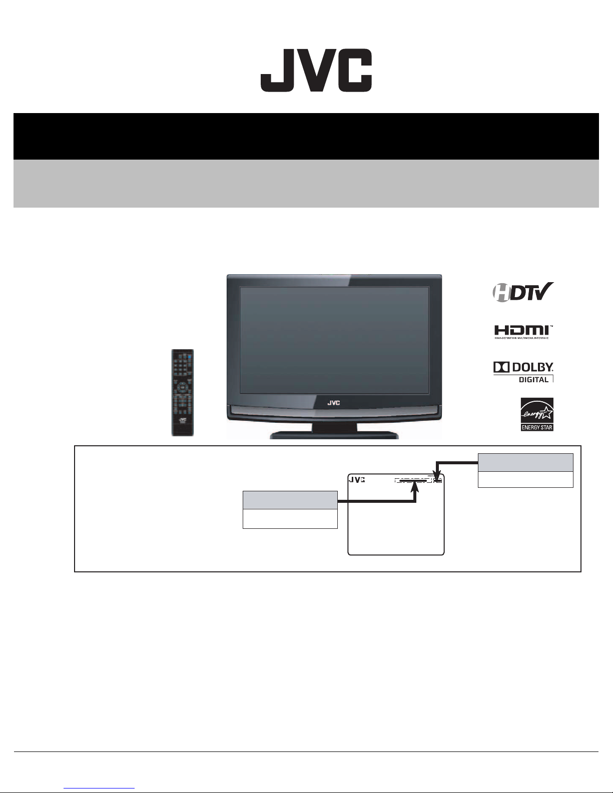
LT-19D200/AK
HIGH DEFINITION TELEVISION
There may be multiple versions of
this TV model.
The TV version is identified by the
letters next to the model number
on the TV's Rating.
(See illustration).
Use the service manual that
matches the version of the TV.
COPYRIGHT © 2009 Victor Company of Japan, Limited
MODEL NAME
LT-19D200
MODEL NO.
RATING LABEL (REAR)
TABLE OF CONTENTS
1 PRECAUTION. . . . . . . . . . . . . . . . . . . . . . . . . . . . . . . . . . . . . . . . . . . . . . . . . . . . . . . . . . . . . . . . . . . . . . . . . 1-3
2 SPECIFIC SERVICE INSTRUCTIONS . . . . . . . . . . . . . . . . . . . . . . . . . . . . . . . . . . . . . . . . . . . . . . . . . . . . . . 1-5
3 DISASSEMBLY . . . . . . . . . . . . . . . . . . . . . . . . . . . . . . . . . . . . . . . . . . . . . . . . . . . . . . . . . . . . . . . . . . . . . . . 1-8
4 ADJUSTMENT . . . . . . . . . . . . . . . . . . . . . . . . . . . . . . . . . . . . . . . . . . . . . . . . . . . . . . . . . . . . . . . . . . . . . . . 1-14
5 TROUBLESHOOTING . . . . . . . . . . . . . . . . . . . . . . . . . . . . . . . . . . . . . . . . . . . . . . . . . . . . . . . . . . . . . . . . . 1-19
VERSION
AK
COPYRIGHT © 2009 Victor Company of Japan, Limited
No.YA711<Rev.002>
2009/8
Page 2
SPECIFICATION
Items Contents
Dimensions ( W × H × D ) 47.75 cm × 36.58 cm × 21.0 cm (18.8" × 14.5" × 8.3") [with stand]
Mass 4.5 kg (10.0 lbs) [with stand]
Power Input AC120 V , 60 Hz
Power Consumption 65 W (Max)
TV RF System
(Analog / Digital)
Color System (Analog) NTSC
Stereo System (Analog) BTSC (Multi Channel Sound)
Teletext System (Analog) Closed caption (T1-T4 / CC1-CC4)
TV Receiving Channels
and Frequency (Analog)
TV / CATV Total Channel 191 Channels
Intermediate Frequency
(Analog)
Color Sub Carrier Frequency (Analog) 3.58 MHz
LCD Panel 19" class (18.5" Diagonal) wide aspect (16 : 9)
Display Pixels Horizontal : 1366 dots × Vertical : 768 dots (W-XGA)
Audio Power Output 1 W + 1 W
Speaker Oval type × 2
Discs (Playback compatibility) DVD video, DVD-RW/-R, DVD+RW/+R, audio CD, video CD, CD-RW/-R
Frequency response DVD (linear sound) 20 Hz to 20 kHz (sample rate: 48 kHz), 20 Hz to 44 kHz (sample rate: 96 kHz)
Signal-to-noise ratio (S/N ratio) CD: 90 dB (JEITA)
Total distortion factor DVD 1 KHz 0.007% (JEITA)
Antenna Terminal
(VHF/UHF, ATSC / DIGITAL CABLE IN)
Video / Audio Input
[VIDEO]
Video / Audio Input
[COMPONENT]
Digital Input Digital(Video/Audio) HDMI 2-row 19pin connector × 1
PC (RGB) Input Video D-sub 15 pin × 1
Digital Audio output 500 mV (rms), Coaxial × 1
Remote Control Unit RM-C2152 (AA/R6 battery × 2)
Component Video
VHF Low
VHF High
Video IF
Sound IF
S-Video Mini-DIN 4 pin × 1
1080i / 720p
480p / 480i
Analog (Audio) 500mV(rms) (-4dBs), high impedance, RCA pin jack × 2
Design & specifications are subject to change without notice.
47.75 cm × 33.04 cm × 13.47 cm (18.8" × 13.1" × 5.4") [without stand]
4.1 kg (9.1 lbs) [without stand]
Analog
CCIR (M)
Digital
ATSC terrestrial / Digital cable
02 ch - 06 ch : 54 MHz - 88 MHz
07 ch - 13 ch : 174 MHz - 216 MHz
UHF
14 ch - 69 ch : 470 MHz - 806 MHz
CATV
54 MHz - 804 MHz
Low Band : 02 - 06
High Band : 07 - 13
Mid Band : 14 - 22
Super Band : 23 - 36
Hyper Band : 37 - 64
Ultra Band : 65 - 94, 100 - 135
Sub Mid Band : 01, 96 - 99
45.75 MHz
41.25 MHz (4.5 MHz)
CD 20 Hz to 20 kHz
CD 1 KHz 0.007% (JEITA)
F-type connector, 75Ω unbalanced, coaxial × 1
Y: 1 V (p-p), Positive (Negative sync.), 75 Ω
C: 0.286V (p-p) (Burst signal), 75 Ω
Video 1 V (p-p), Positive (Negative sync.), 75 Ω, RCA pin jack × 1
Audio 500 mV (rms), High impedance, RCA pin jack × 2
RCA pin jack × 3
Y : 1 V (p-p) (Sync signal: 0.35V(p-p), 3-value sync.), 75 Ω
Pb/Pr : ±0.35V(p-p), 75 Ω
Y : 1 V (p-p), Positive (Negative sync.), 75 Ω
Cb/Cr : 0.7V(p-p), 75 Ω
Audio 500 mV (rms), High impedance, RCA pin jack × 2
(Digital-input terminal is not compatible with picture signals of personal computer)
Video: Supported format: 1080i / 720p / 480p / 480i
Audio: 2ch L-PCM, 32 / 44.1 / 48 KHz, 16 / 20 / 24 bit
R/G/B : 0.7 V (p-p), 75Ω
HD / VD : 1 V (p-p) to 5 V (p-p), high impedance
Audio 3.5 mm stereo mini jack × 1
1-2 (No.YA711<Rev.002>)
Page 3

SECTION 1
PRECAUTION
1.1 SAFETY PRECAUTIONS
(1) The design of this product contains special hardware,
many circuits and components specially for safety
purposes. For continued protection, no changes should be
made to the original design unless authorized in writing by
the manufacturer. Replacement parts must be identical to
those used in the original circuits. Service should be
performed by qualified personnel only.
(2) Alterations of the design or circuitry of the products should
not be made. Any design alterations or additions will void
the manufacturer's warranty and will further relieve the
manufacturer of responsibility for personal injury or
property damage resulting therefrom.
(3) Many electrical and mechanical parts in the products have
special safety-related characteristics. These
characteristics are often not evident from visual inspection
nor can the protection afforded by them necessarily be
obtained by using replacement components rated for
higher voltage, wattage, etc. Replacement parts which
have these special safety characteristics are identified in
the parts list of Service manual. Electrical components
having such features are identified by shading on the
schematics and by ( ) on the parts list in Service
manual. The use of a substitute replacement which does
not have the same safety characteristics as the
recommended replacement part shown in the parts list of
Service manual may cause shock, fire, or other hazards.
(4) Don't short between the LIVE side ground and
ISOLATED (NEUTRAL) side ground or EARTH side
ground when repairing.
Some model's power circuit is partly different in the GND.
The difference of the GND is shown by the LIVE : ( ) side
GND, the ISOLATED (NEUTRAL) : ( ) side GND and
EARTH : ( ) side GND.
Don't short between the LIVE side GND and ISOLATED
(NEUTRAL) side GND or EARTH side GND and never
measure the LIVE side GND and ISOLATED (NEUTRAL)
side GND or EARTH side GND at the same time with a
measuring apparatus (oscilloscope etc.). If above note will
not be kept, a fuse or any parts will be broken.
(5) When service is required, observe the original lead dress.
Extra precaution should be given to assure correct lead
dress in the high voltage circuit area. Where a short circuit
has occurred, those components that indicate evidence of
overheating should be replaced. Always use the
manufacturer's replacement components.
(6) Isolation Check (Safety for Electrical Shock Hazard)
After re-assembling the product, always perform an
isolation check on the exposed metal parts of the cabinet
(antenna terminals, video/audio input and output terminals,
Control knobs, metal cabinet, screw heads, earphone jack,
control shafts, etc.) to be sure the product is safe to operate
without danger of electrical shock.
a) Dielectric Strength Test
The isolation between the AC primary circuit and all metal
parts exposed to the user, particularly any exposed metal
part having a return path to the chassis should withstand a
voltage of 3000V AC (r.m.s.) for a period of one second. (.
. . . Withstand a voltage of 1100V AC (r.m.s.) to an
appliance rated up to 120V, and 3000V AC (r.m.s.) to an
appliance rated 200V or more, for a period of one second.)
This method of test requires a test equipment not generally
found in the service trade.
b) Leakage Current Check
Plug the AC line cord directly into the AC outlet (do not use
a line isolation transformer during this check.). Using a
"Leakage Current Tester", measure the leakage current
from each exposed metal part of the cabinet, particularly
any exposed metal part having a return path to the chassis,
to a known good earth ground (water pipe, etc.). Any
leakage current must not exceed 0.5mA AC (r.m.s.).
However, in tropical area, this must not exceed 0.2mA AC
(r.m.s.).
Alternate Check Method
Plug the AC line cord directly into the AC outlet (do not
use a line isolation transformer during this check.). Use
an AC voltmeter having 1000Ω per volt or more
sensitivity in the following manner. Connect a 1500Ω
10W resistor paralleled by a 0.15µF AC-type capacitor
between an exposed metal part and a known good earth
ground (water pipe, etc.). Measure the AC voltage
across the resistor with the AC voltmeter. Move the
resistor connection to each exposed metal part,
particularly any exposed metal part having a return path
to the chassis, and measure the AC voltage across the
resistor. Now, reverse the plug in the AC outlet and
repeat each measurement. Any voltage measured must
not exceed 0.75V AC (r.m.s.). This corresponds to
0.5mA AC (r.m.s.).
However, in tropical area, this must not exceed 0.3V AC
(r.m.s.). This corresponds to 0.2mA AC (r.m.s.).
AC VOLTMETER
(HAVING 1000 /V,
OR MORE SENSITIVITY)
0.15 F AC-TYPE
GOOD EARTH GROUND
1500 10W
PLACE THIS PROBE
ON EACH EXPOSED
ME TAL PAR T
(No.YA711<Rev.002>)1-3
Page 4
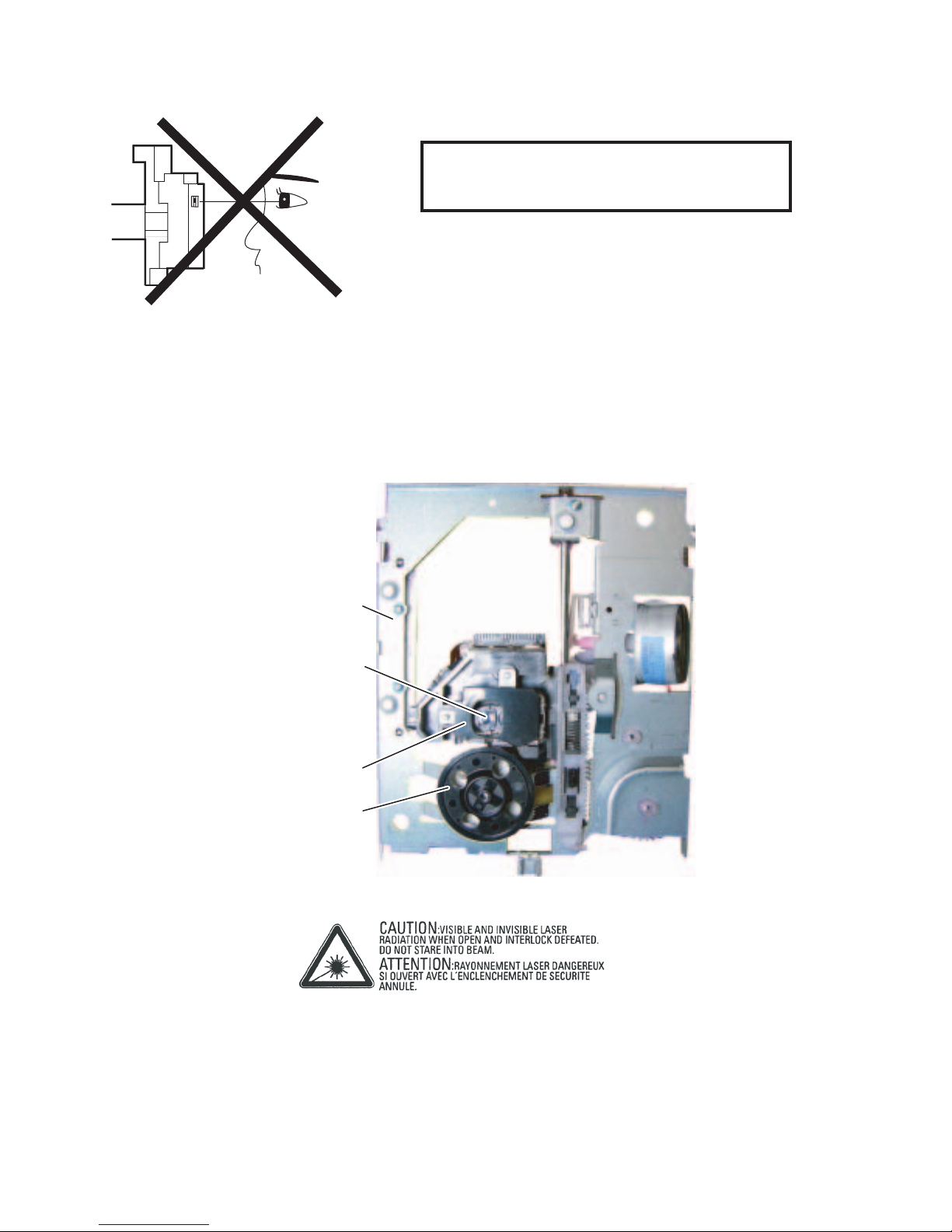
1.2 LASER BEAM SAFETY PRECAUTIONS
This DVD player uses a pickup that emits a laser beam.
Do not look directly at the laser beam coming
from the pickup or allow it to strike against your
skin.
The laser beam is emitted from the location shown in the figure. When checking the laser diode, be sure to keep your eyes at least 30
cm away from the pickup lens when the diode is turned on. Do not look directly at the laser beam.
CAUTION:
Use of controls and adjustments, or doing procedures other than those specified herein, may result in hazardous radiation exposure.
Drive Mechanism
Assembly
Laser Beam Radiation
Laser Pickup
Turntable
Location: Top of LCD module.
1-4 (No.YA711<Rev.002>)
Page 5
SECTION 2
SPECIFIC SERVICE INSTRUCTIONS
2.1 STANDARD NOTES FOR SERVICING
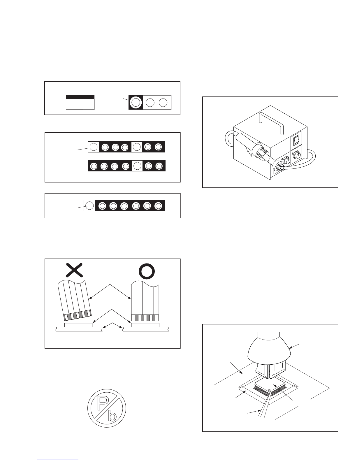
2.1.1 CIRCUIT BOARD INDICATIONS
(1) The output pin of the 3 pin Regulator ICs is indicated as
shown.
Top View
Bottom View
Input
Out
(2) For other ICs, pin 1 and every fifth pin are indicated as
shown.
In
5
Pin 1
10
(3) The 1st pin of every male connector is indicated as shown.
Pin 1
2.1.2 INSTRUCTIONS FOR CONNECTORS
(1) When you connect or disconnect the FFC (Flexible Foil
Connector) cable, be sure to first disconnect the AC cord.
(2) FFC (Flexible Foil Connector) cable should be inserted
parallel into the connector, not at an angle.
FFC Cable
Connector
CBA
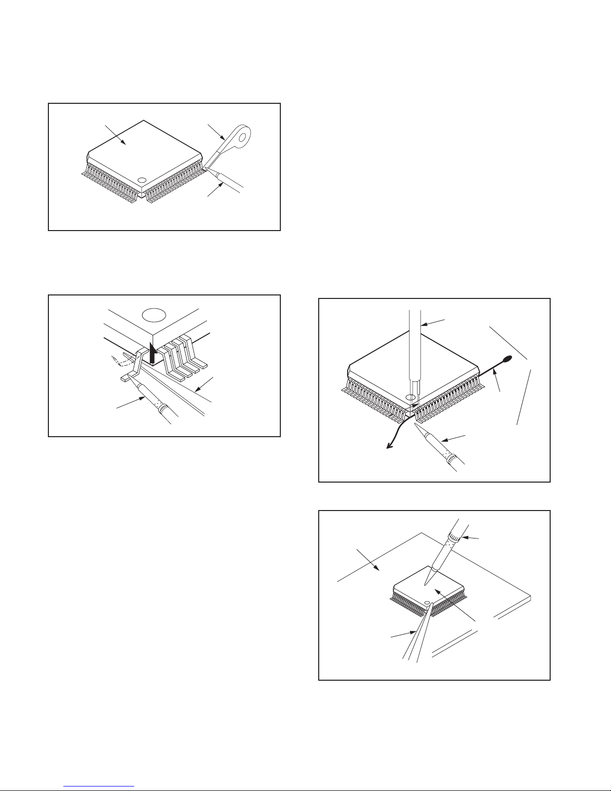
2.1.4 HOW TO REMOVE / INSTALL FLAT PACK-IC
2.1.4.1 REMOVAL
WITH HOT-AIR FLAT PACK-IC DESOLDERING MACHINE:
(1) Prepare the hot-air flat pack-IC desoldering machine,
then apply hot air to the Flat Pack-IC (about 5 to 6
seconds). (Fig.2-1)
Fig.2-1
(2) Remove the flat pack-IC with tweezers while applying
the hot air.
(3) Bottom of the flat pack-IC is fixed with glue to the PWB;
when removing entire flat pack-IC, first apply soldering
iron to center of the flat pack-IC and heat up. Then
remove (glue will be melted). (Fig.2-6)
(4) Release the flat pack-IC from the PWB using tweezers.
(Fig.2-6)
CAUTION:
(1) The Flat Pack-IC shape may differ by models. Use an
appropriate hot-air flat pack-IC desoldering machine,
whose shape matches that of the Flat Pack-IC.
(2) Do not supply hot air to the chip parts around the flat
pack-IC for over 6 seconds because damage to the
chip parts may occur. Put masking tape around the flat
pack-IC to protect other parts from damage. (Fig.2-2)
(3) The flat pack-IC on the PWB is affixed with glue, so be
careful not to break or damage the foil of each pin or
the solder lands under the IC when removing it.
* Be careful to avoid a short circuit.
2.1.3 PB (LEAD) FREE SOLDER
Pb free mark will be found on PCBs which use Pb free
solder. (Refer to figure.) For PCBs with Pb free mark, be sure
to use Pb free solder. For PCBs without Pb free mark, use
standard solder.
Pb free mark
CBA
Masking
Tape
Tweezers
Hot-air
Flat Pack-IC
Desoldering
Machine
Flat Pack-IC
Fig.2-2
(No.YA711<Rev.002>)1-5
Page 6
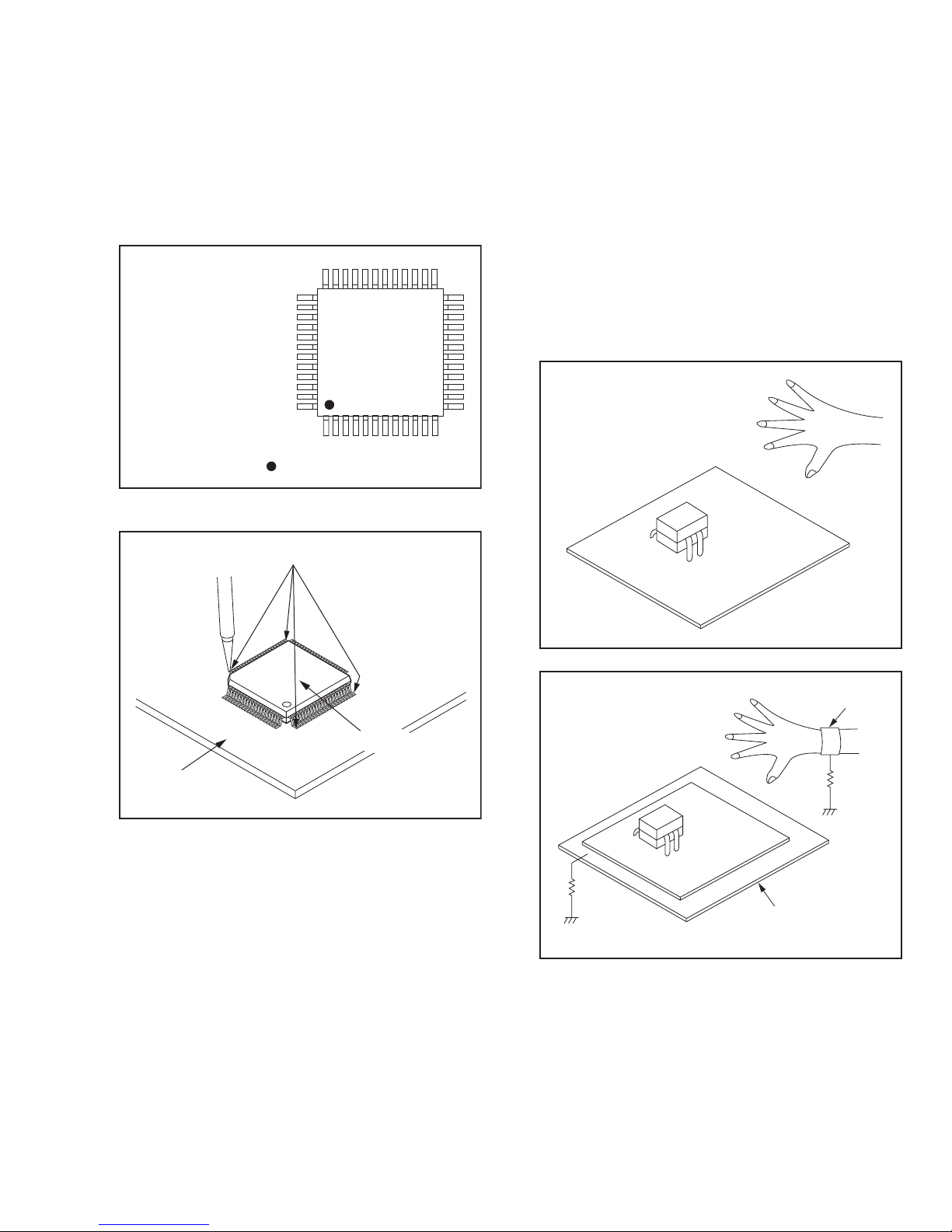
WITH SOLDERING IRON:
(1) Using desoldering braid, remove the solder from all pins
of the flat pack-IC. When you use solder flux which is
applied to all pins of the flat pack-IC, you can remove it
easily. (Fig.2-3)
Flat Pack-IC
Desoldering Braid
Soldering Iron
Fig.2-3
(2) Lift each lead of the flat pack-IC upward one by one,
using a sharp pin or wire to which solder will not adhere
(iron wire). When heating the pins, use a fine tip
soldering iron or a hot air desoldering machine. (Fig.2-4)
WITH IRON WIRE:
(1) Using desoldering braid, remove the solder from all pins
of the flat pack-IC. When you use solder flux which is
applied to all pins of the flat pack-IC, you can remove it
easily. (Fig.2-3)
(2) Affix the wire to a workbench or solid mounting point, as
shown in Fig.2-5.
(3) While heating the pins using a fine tip soldering iron or
hot air blower, pull up the wire as the solder melts so as
to lift the IC leads from the PWB contact pads as shown
in Fig.2-5.
(4) Bottom of the flat pack-IC is fixed with glue to the PWB;
when removing entire flat pack-IC, first apply soldering
iron to center of the flat pack-IC and heat up. Then
remove (glue will be melted). (Fig.2-6)
(5) Release the flat pack-IC from the PWB using tweezers.
(Fig.2-6)
NOTE:
When using a soldering iron, care must be taken to ensure
that the flat pack-IC is not being held by glue. When the flat
pack-IC is removed from the PWB, handle it gently because
it may be damaged if force is applied.
Hot Air Blower
Sharp
Pin
Fine Tip
Soldering Iron
Fig.2-4
(3) Bottom of the flat pack-IC is fixed with glue to the PWB;
when removing entire flat pack-IC, first apply soldering
iron to center of the flat pack-IC and heat up. Then
remove (glue will be melted). (Fig.2-6)
(4) Release the flat pack-IC from the PWB using tweezers.
(Fig.2-6)
To Solid
Mounting Point
CBA
Tweezers
or
Iron Wire
Soldering Iron
Fig.2-5
Fine Tip
Soldering Iron
Flat Pack-IC
1-6 (No.YA711<Rev.002>)
Fig.2-6
Page 7
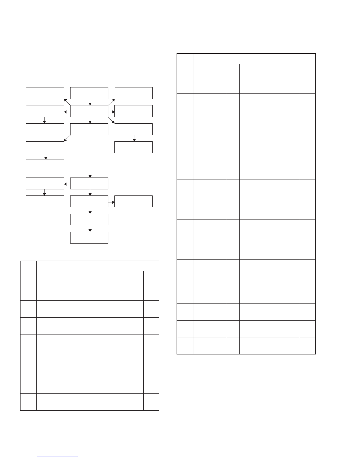
2.1.4.2 INSTALLATION
(1) Using desoldering braid, remove the solder from the foil of
each pin of the flat pack-IC on the PWB so you can install
a replacement flat pack-IC more easily.
(2) The z mark on the flat pack-IC indicates pin 1. (See Fig.2-
7.) Be sure this mark matches the 1 on the PCB when
positioning for installation. Then presolder the four corners
of the flat pack-IC. (See Fig.2-8.)
(3) Solder all pins of the flat pack-IC. Be sure that none of the
pins have solder bridges.
Example :
Pin 1 of the Flat Pack-IC
is indicated by a " " mark.
Fig.2-7
2.1.5 INSTRUCTIONS FOR HANDLING SEMICONDUCTORS
Electrostatic breakdown of the semi-conductors may occur due
to a potential difference caused by electrostatic charge during
unpacking or repair work.
2.1.5.1 Ground for Human Body
Be sure to wear a grounding band (1MΩ) that is properly
grounded to remove any static electricity that may be charged on
the body.
2.1.5.2 Ground for Workbench
Be sure to place a conductive sheet or copper plate with proper
grounding (1MΩ) on the workbench or other surface, where the
semi-conductors are to be placed. Because the static electricity
charge on clothing will not escape through the body grounding
band, be careful to avoid contacting semi-conductors with your
clothing.
<I
ncorrec
t
>
CBA
Presolder
Fig.2-8
Flat Pack-IC
<
C
orrec
1M
CBA
t
>
Grounding Band
1M
CBA
Conductive Sheet or
Copper Plate
(No.YA711<Rev.002>)1-7
Page 8
SECTION 3
DISASSEMBLY
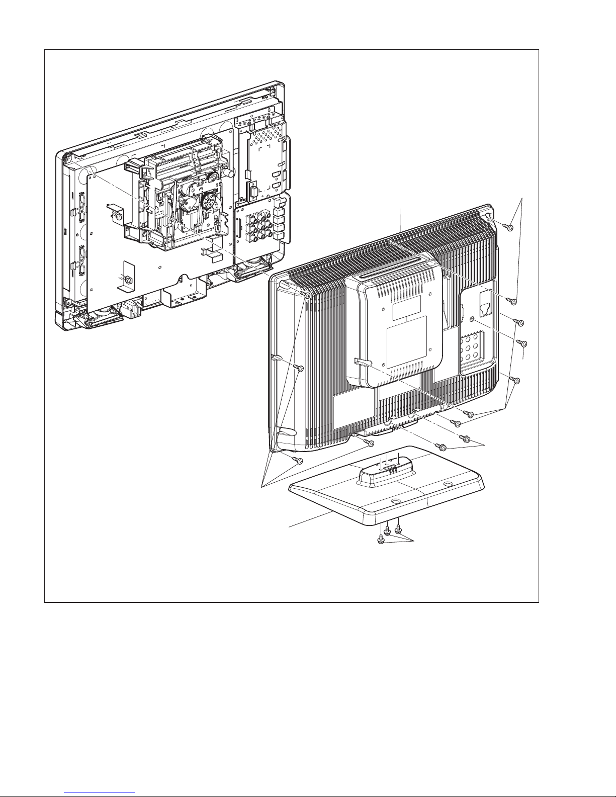
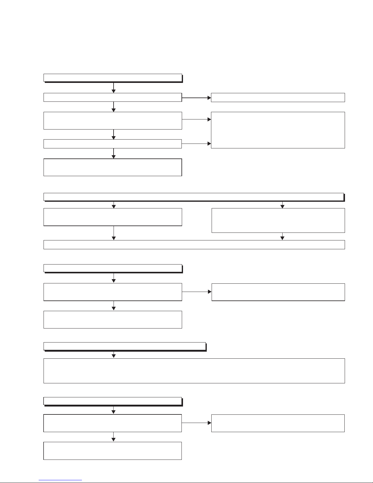
3.1 DISASSEMBLY FLOWCHART
This flowchart indicates the disassembly steps for the cabinet
parts, and the PWB in order to gain access to item(s) to be serviced. When reassembling, follow the steps in reverse order.
Bend, route and dress the cables as they were.
[17] Junction-A
PWB
[6] Jack Holder
(D)
[7] Digital Main
PWB Unit
[4] DVD
Mechanism
[5] DVD Main
PWB Unit
[13] Speaker
Holder (s)
[14] Speaker (s)
3.2 DISASSEMBLY METHOD
[1] Stand
Assembly
[2] Rear Cabinet
[3] DVD Holder
[10] Main PWB
[11] Stand Holder
[12] LCD Module
Assembly
[19] Front
Cabinet
[15] Junction-C
PWB
[16] Junction-B
PWB
[8] Jack Holder
(A)
[9] Jack PWB
[18] Function
PWB
Step/
Loc.
Part
No.
Jack
[6]
Holder(D)
Digital Main
[7]
PWB UnitD3D5
Jack
[8]
Holder(A)
[9] Jack PWB
[10] Main PWB
Stand
[11]
Holder
LCD
[12]
Module
Assembly
Speaker
[13]
Holder(s)
Removal
Remove/*Unhook/
Fig.
No.
Unlock/Release/
Unplug/Unclamp/
Note
Desolder
D3 (S-8) ---
4(S-9), (S-10),
4(S-11), 2(H-1),
*CN301, *CN302,
*CN303, *CN3902,
Shield Box
D3 (S-12) ---
D3D54(S-13), CN702,
*CN861A
7(S-14), *CN102,
D3
*CN201, *CN862A,
D5
*CN1001, *CN1002
D4 2(S-15), (S-16) ---
D4 --------------- ---
D4 4(S-17) ---
---
---
---
Step/
Loc.
Part
No.
Stand
[1]
Assembly
Rear
[2]
Cabinet
[3] DVD Holder
DVD
[4]
MechanismD2D5
DVD Main
[5]
PWB Unit
Removal
Remove/*Unhook/
Fig.
No.
Unlock/Release/
Unplug/Unclamp/
Note
Desolder
D1 3(S-1) ---
D1 10(S-2), 2(S-3), (S-4) ---
D2D54(S-5), 3(S-6),
*CN901, *CN902
(S-7), *CN201,
*CN301, *CN801
D2 --------------- ---
---
[14] Speaker(s) D4 --------------- ---
Junction-C
[15]
PWB
Junction-B
[16]
PWB
Junction-A
[17]
PWB
Function
[18]
PWB
Front
[19]
Cabinet
1
2
(1) (2) (3) (4) (5)
D4
Desolder ---
D5
D4
Desolder ---
D5
D4
Desolder ---
D5
D4
2(S-18) ---
D5
D4 --------------- ---
3
4
5
6
1-8 (No.YA711<Rev.002>)
Page 9
NOTE;
(1) Order of steps in procedure. When reassembling, follow
the steps in reverse order. These numbers are also used
as the Identification (location) No. of parts in figures.
(2) Parts to be removed or installed.
(3) Fig. No. showing procedure of part location
(4) Identification of parts to be removed, unhooked, un-
locked, released, unplugged, unclamped, or desoldered.
P = Spring, L = Locking Tab, S = Screw, H = Hex Screw,
CN = Connector * = Unhook, Unlock, Release, Unplug,
or Desolder e.g. 2(S-2) = two Screws (S-2), 2(L-2) = two
Locking Tabs (L-2)
(5) Refer to the following "Reference Notes in the Table."
REFERENCE NOTES
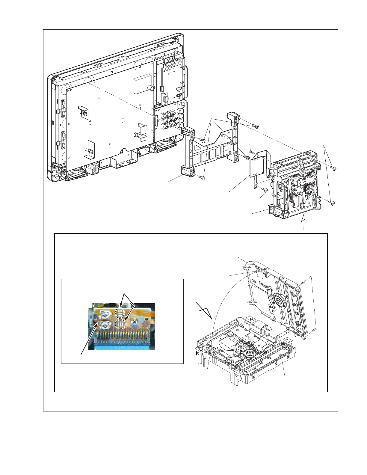
(1) CAUTION 1: Electrostatic breakdown of the laser diode
in the optical system block may occur as a potential dif-
ference caused by electrostatic charge accumulated on
cloth, human body etc., during unpacking or repair work.
To avoid damage of pickup follow next procedures.
a) Short the three short lands of FPC cable with sol-
der before removing the FFC cable (CN201) from
it. If you disconnect the FFC cable (CN201), the laser diode of pickup will be destroyed. (Fig. D2)
b) Disconnect the Connectors (CN301), and
(CN801). Remove Screw (S-7) and remove the
DVD Main PWB Unit. (Fig. D2)
(2) Reassembly Notes of New DVD Mechanism:
a) To remove the Chassis Cover, remove two screws
A as shown in Fig. D2.
b) To avoid damage of the pickup unit (laser diode),
confirm that the three short lands (either of two
places) are shorted out by soldering between them
as shown in View A in Fig. D2.
c) Connect the FFC cables of the new DVD Mecha-
nism to the three connectors (CN201, CN301,
CN801) on the DVD Main PWB Unit.
d) After confirming that the FFC cables are securely
connected to the three connectors, remove the solder from the three short lands. If the solder is not
removed, the laser diode will not light and it will not
be possible to read discs.
e) Insert the pin A on the Chassis Cover into the hole
A on the Main Chassis as shown in Fig. D2. Then
tighten two screws A to install the Chassis Cover.
(3) CAUTION 2: When reassembling, confirm the FFC cable
(CN201) is connected completely. Then remove the sol-
der from the three short lands of FPC cable. (Fig. D2)
(4) How to eject a disc in emergency
Press and hold [EJECT] on the unit for more than 5 sec-
onds.
(5) How to eject manually 1
a) Remove the Rear Cabinet.
b) Rotate the gear in the direction of the arrow as
shown below.
B
View for B
The gear is turned to the direction
of the arrow.
(6) How to eject manually 2
a) Remove the Rear Cabinet.
b) To remove the DVD Main PWB Unit, remove a
screw (S-7) in Fig. D2. Do not disconnect connectors.
c) To remove the Chassis Cover, remove two screws
A as shown in Fig. D2.
d) Remove a disc.
(No.YA711<Rev.002>)1-9
Page 10
[2] Rear Cabinet
(S-2)
(S-4)
(S-2)
(S-3)
[1] Stand Assembly
1-10 (No.YA711<Rev.002>)
(S-2)
(S-1)
Fig. D1
Page 11
(S-5)
(S-7)
[3] DVD Holder
[5] DVD Main PWB unit
(S-6)
[4] DVD Mechanism
A
Remove two screws A, then short the three short lands by soldering as shown in View for A.
Chassis Cover
Pin A
Either of two places
Screws A
A
(S-6)
FPC Cable
View for A
Hole A
Main Chassis
Fig. D2
(No.YA711<Rev.002>)1-11
Page 12
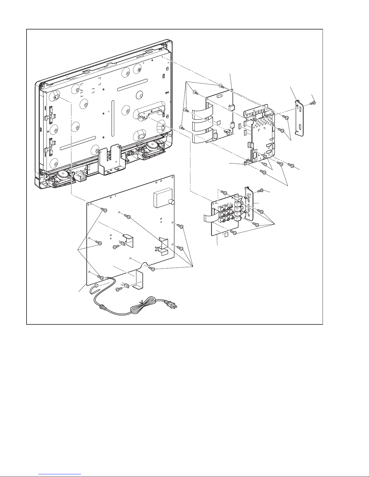
(S-11)
[7] Digital Main
PWB Unit
Shield Box
[6] Jack Holder(D)
(S-8)
(S-9)
(H-1)
(S-12)
(S-10)
(S-9)
[8] Jack Holder(A)
(S-13)
(S-14)
[10] Main PWB
[9] Jack PWB
(S-14)
Fig. D3
1-12 (No.YA711<Rev.002>)
Page 13
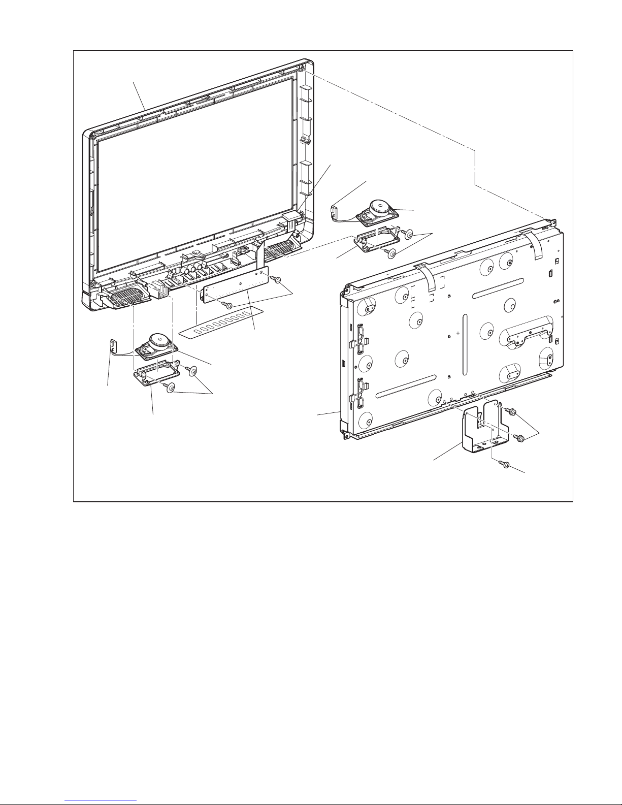
[19] Front Cabinet
[17] Junction-A
CBA
[15] Junction-C
CBA
[14] Speaker
(S-17)
[13] Speaker
Holder
(S-18)
[18] Function CBA
[16] Junction
-B CBA
[13] Speaker
Holder
[14] Speaker
(S-17)
[12] LCD Module
Assembly
(S-15)
[11] Stand Holder
(S-16)
Fig. D4
(No.YA711<Rev.002>)1-13
Page 14
SECTION 4
ADJUSTMENT
4.1 GENERAL NOTE: "PWB" IS ABBREVIATION FOR
"CIRCUIT BOARD ASSEMBLY."
NOTE:
Electrical adjustments are required after replacing circuit components and certain mechanical parts. It is important to perform these adjustments only after all repairs and replacements
have been completed. Also, do not attempt these adjustments
unless the proper equipment is available.
4.2 TEST EQUIPMENT REQUIRED
(1) NTSC Pattern Generator (Color Bar W/White Window, Red
Color, Dot Pattern, Gray Scale, Monoscope, Multi-Burst)
(2) Remote control unit
(3) Color Analyzer
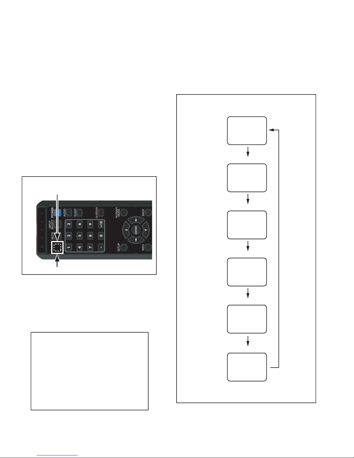
4.3 HOW TO MAKE THE SERVICE REMOTE CONTROL
UNIT:
Cut "A" portion of the attached remote control unit as shown in
Fig. 1.
service button
(There is a button under the plastic housing.)
4.5 PURITY CHECK MODE
This mode cycles through full-screen displays of red, green, blue,
and white to check for non-active pixels.
(1) Enter the Service mode.
(2) Each time pressing [7] button on the service remote control
unit, the display changes as follows.
Purity Check Mode
White mode
[7] button
[7] button
Black mode
[7] button
Red mode
A
4.4 HOW TO SET UP THE SERVICE MODE:
Service mode:
(1) Use the service remote control unit.
(2) Turn the power on.
(3) Press the service button on the service remote control
unit. The following screen appears.
"*" differs depending on the models.
Code :
***********-***
Pic code :
**-***-**-*****-***
MIPS :
Push 0key
Tuner :
****-*****-****
safety_Non
Safety :
[7] button
Green mode
Fig. 1
[7] button
Blue mode
[7] button
White 20% mode
Note:
When entering this mode, the default setting is White mode.
1-14 (No.YA711<Rev.002>)
Page 15
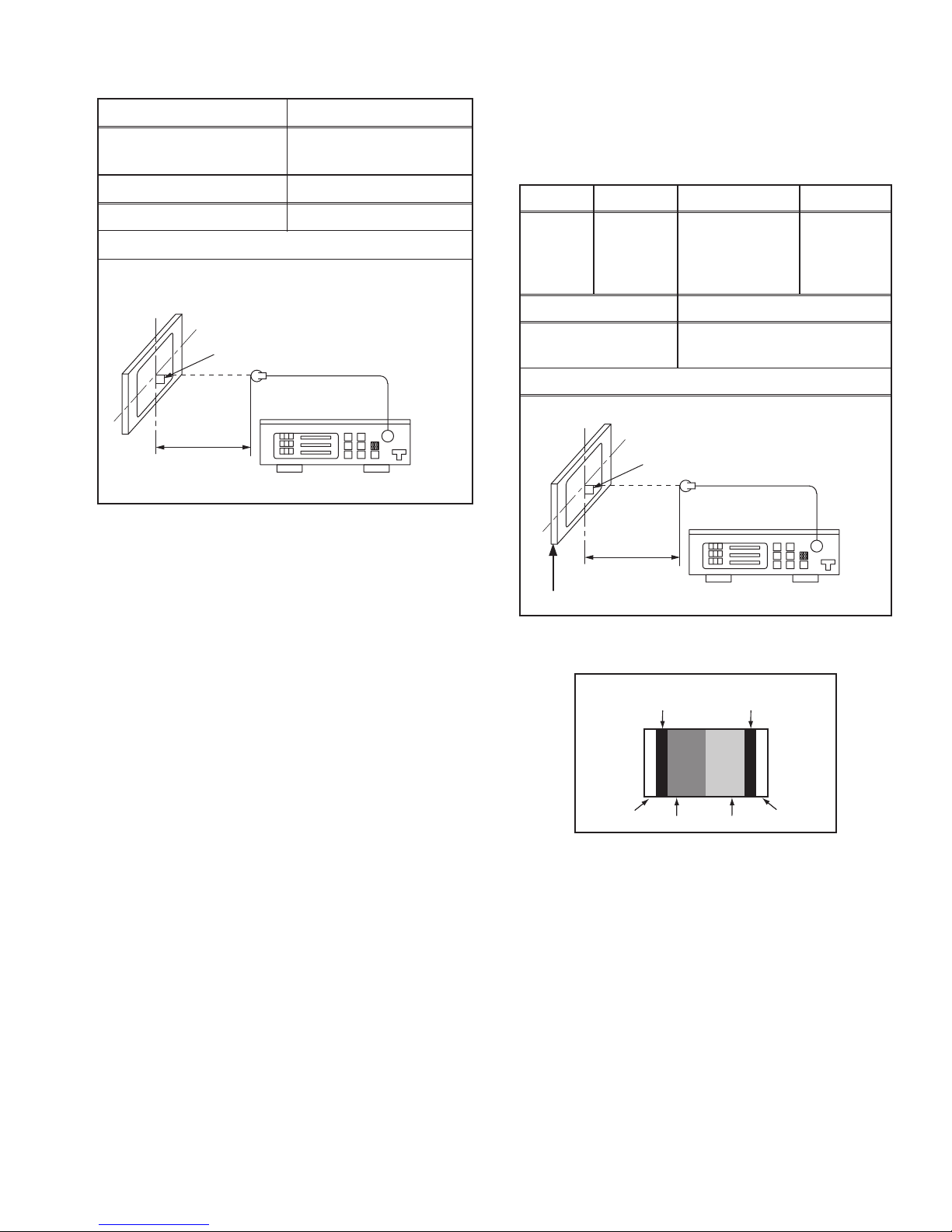
4.6 VCOM ADJUSTMENT
Test Point Adj. Point
Screen
M. EQ. Spec.
Color analyzer See below
To avoid interference from ambinent
light, this adjustment should be
performed in a dark room.
Perpendicularity
L = 3 cm
[CHANNEL UP/DOWN ]
buttons
Figure
Color Analyzer
4.7 WHITE BALANCE ADJUSTMENT
The white balance adjustment should be performed when
replacing the LCD Panel or Digital PWB.
Purpose: To mix red, green and blue beams correctly for pure
white.
Symptom of Misadjustment: White becomes bluish or reddish.
Test Point
Screen
Adj. Point Mode Input
[VOLUME
DOWN]
button
[VIDEO1]
C/D
White Raster
(APL 70%)
or
(APL 40%)
M. EQ. Spec.
Pattern Generator,
Color analyzer
x= 0.272 ± 0.005
y= 0.278 ± 0.005
Figure
To avoid interference from ambinent
light, this adjustment should be
performed in a dark room.
Perpendicularity
(1) Operate the unit for more than 20 minutes.
(2) Set the color analyzer and bring the optical receptor to the
center on the LCD-Panel surface after zero point calibration as shown above. Note: The optical receptor must be
set perpendicularly to the LCD Panel surface.
(3) Enter the Service mode.
(4) Press [3] button on the service remote control unit.
(5) Press [CHANNEL UP/DOWN] buttons on the service re-
mote control unit so that the color analyzer value becomes
minimum.
L = 3 cm
INPUT: WHITE 70%, 40%
(1) Operate the unit for more than 20 minutes.
(2) Input the White Raster(70%=70IRE, 40%=40IRE).
INPUT SIGNAL
0IRE 0IRE
100IRE
40%=40IRE
(3) Set the color analyzer to the CHROMA mode and bring the
optical receptor to the center on the LCD-Panel surface after zero point calibration as shown above.
Note: The optical receptor must be set perpendicularly to
the LCD Panel surface.
(4) Enter the Service mode. Press [VOLUME DOWN] button
on the service remote control unit and select "C/D" mode.
(5) [CUTOFF]
Press [1] button to select “COR” for Red Cutoff adjustment.
Press [3] button to select “COB” for Blue Cutoff adjustment.
[DRIVE]
Press [4] button to select “DR” for Red Drive adjustment.
Press [6] button to select “DB” for Blue Drive adjustment.
(6) In each color mode, press [CHANNEL UP/DOWN] buttons
to adjust the values of color.
(7) Adjust Cutoff and Drive so that the color temperature be-
comes 12000°K (x= 0.272 / y= 0.278 ±0.005).
Color Analyzer
Low
Hight
Light
Light
70%=70IRE
100IRE
(No.YA711<Rev.002>)1-15
Page 16

4.8 HOW TO INITIALIZE THE LCD TV/DVD
The purpose of initialization is to place the set in a new out of box condition. The customer will be prompted to
select a language and program channels after the set has been initialized.
To put the program back at the factory-default, initialize the LCD TV/DVD using the following procedure.
4.8.1 DVD SECTION
Turn the power on.
(1)
(2) To enter the service mode, press the service button on the
service remote control unit.
- To cancel the service mode, press [POWER] button on
the service remote control unit.
(3) To put the LCD TV/DVD into the DVD mode, press [CH RE-
TURN] on the remote control unit.
(4) To put the LCD TV/DVD into the Flash clear mode, press
[INPUT SELECT] buttons on the remote control unit in that
order within five seconds. The following screen appears.
Flash Memory Clear : OK
CHUCKING ON
4.8.2 LCD TV SECTION
(1) Turn the power on.
(2) To enter the service mode, press the service button on the
service remote control unit.
- To cancel the service mode, press [POWER] button on
the service remote control unit.
(3) Press [INFO] button on the service remote control unit to
initialize the LCD television.
(4) "INITIALIZED" will appear in the upper right of the screen.
"INITIALIZED" color will change to green from red when initializing is complete.
When "OK" appears on the screen, the factory default will
be set.
(5) To exit this mode, press[CHANNEL UP/DOWN] button to
go to TV mode, or press [POWER] button to turn the power
off.
1-16 (No.YA711<Rev.002>)
Page 17
4.9 FIRMWARE RENEWAL MODE
4.9.1 DVD SECTION
(1) Turn the power on and press [EJECT] button on the remote
control unit to put the LCD TV/DVD into DVD mode. Then
remove the disc.
(2) To put the LCD TV/DVD into F/W version up mode, press
[9], [8], [7], [6], and [MODE] buttons on the remote control
unit in that order.
Fig. a appears on the screen.
"
" differs depending on the models.
*******
F/W Version Up Mode Model No : ******
Please insert a DISC
for F/W Version Up.
VERSION : *.**
At this time, no button is available.
(6) Remove the disc.
(7) Unplug the AC cord from the AC outlet. Then plug it again.
(8) Press [EJECT] button on the remote control unit to put the
LCD TV/DVD into DVD mode again.
(9) Press [1], [2], [3], [4], and [INFO] buttons on the remote
control unit in that order. Fig. d appears on the screen.
"
" differs depending on the models.
*******
MODEL : ******
Version
Region
: *.**
: *
EXIT: SELECTEEPROM CLEAR : CLEAR
EXIT: SELECT
Fig. a Version Up Mode Screen
(3) Insert the disc for version up into the disc slot.
(4) The LCD TV/DVD enters the F/W version up mode auto-
matically. Fig. b appears on the screen. Make sure to insert
the proper F/W for the state of this model.
"
" differ depending on the models.
*******
(*1)
F/W Version Up Mode Model No : ******
VERSION : ************.***
Reading...
VERSION : *.**
Fig. b Programing Mode Screen
The appearance shown in (*1) of Fig. b is described as follows:
No. Appearance State
1 Reading... Sending files into the memory
2 Erasing... Erasing previous version data
3 Programming... Writing new version data
Fig. d
(10) Press [CLEAR] button on the remote control unit. Fig. e ap-
pears on the screen.
"
" differs depending on the models.
*******
MODEL : ******
Version
Region
: *.**
: *
EXIT: SELECTEEPROM CLEAR : CLEAR
EEPROM CLEAR : OK
Fig. e
When “OK” appears on the screen, the factory default will
be set. Then the firmware renewal mode is complete.
(11) To exit this mode, press [CHANNEL UP/DOWN] button to
go to TV mode, or press [POWER] button to turn the power
off.
(5) After programming is finished, the disc will be ejected auto-
matically. Fig. c appears on the screen and the checksum
will be shown in (*2).
"
" differ depending on the models.
*******
(*2)
F/W Version Up Mode
VERSION : ************.***
Completed
SUM : ****
Model No : ******
VERSION : *.**
Fig. c Completed Program Mode Screen
(No.YA711<Rev.002>)1-17
Page 18
4.9.2 LCD TV SECTION
4.9.2.1 EQUIPMENT REQUIRED
a. USB memory
b. Remote Control Unit
4.9.2.2 FIRMWARE UPDATE PROCEDURE
NOTE:
There are two states (the User Upgrade and the Factory Upgrade) in firmware update.
User Upgrade Upgrade the firmware only. The
setting values are not initialized.
Factory upgrade Upgrade the firmware and initialize
the setting values.
The identification of User Upgrade and Factory Upgrade are
done by the filename.
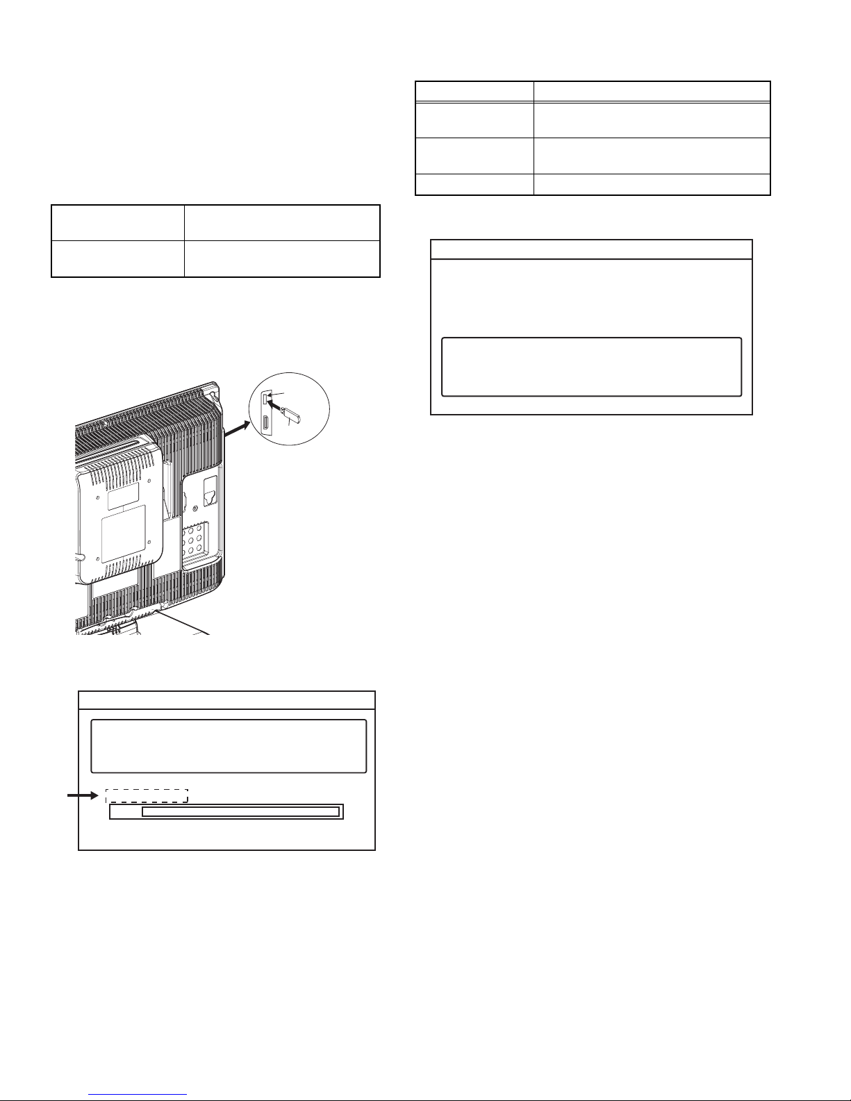
(1) Turn the power off and unplug the AC Cord.
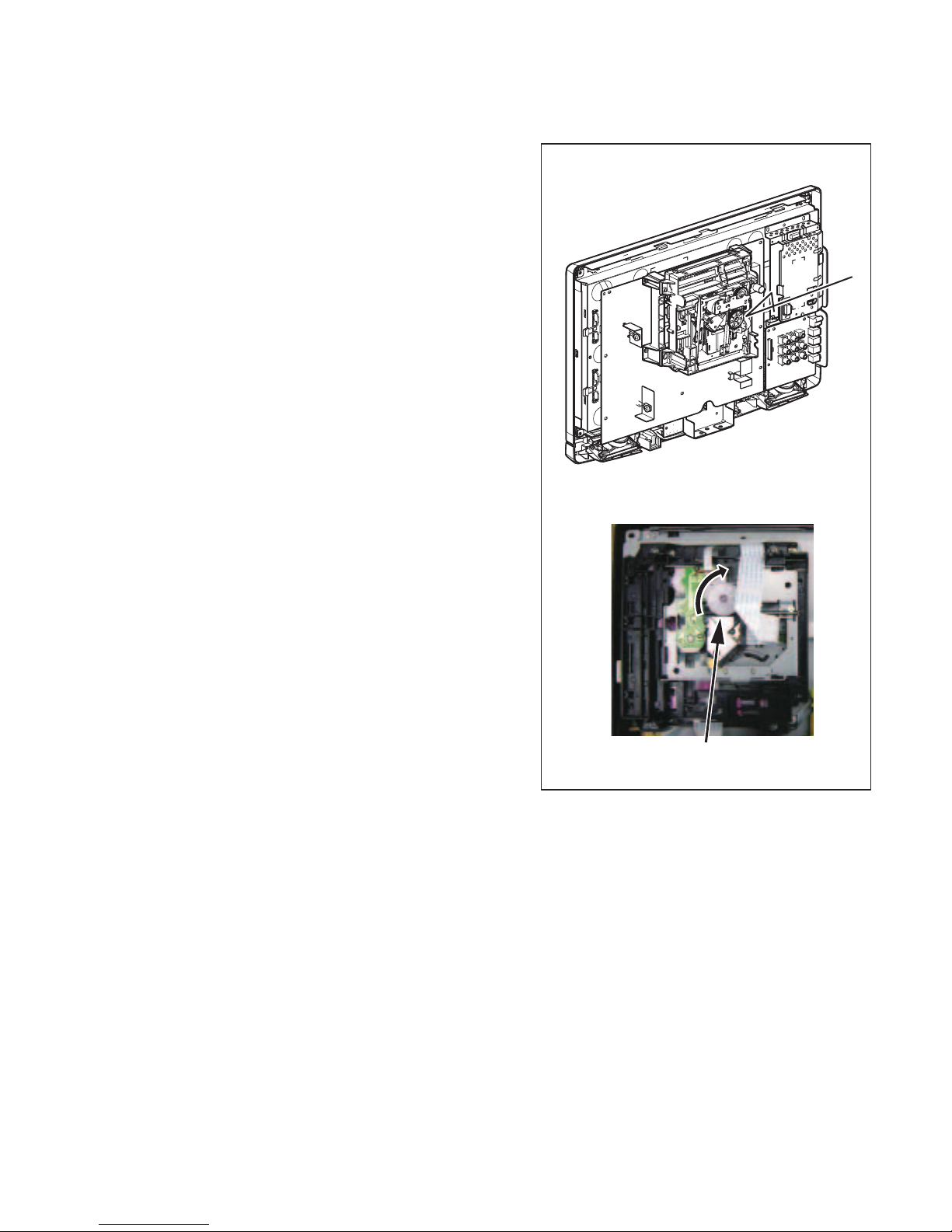
(2) Insert the USB memory to the USB port as shown below.
Rear Cabinet
USB port
The appearance shown in *1 is described as follows.
Appearance State
Downloading... Downloading the firmware from the USB
memory.
Writing... Writing the downloaded firmware in flash
memory.
Checking... Checking the new firmware.
(5) When the firmware update is completed, the following will
appear on the screen.
Software Upgrade
The software upgrade is completed.
Remove USB storage device, unplug and replug power code.
USB Memory
(3) Plug the AC cord in the wall outlet and turn the power on.
(4) The update will start and the following will appear on the
screen.
Software Upgrade
Software upgrade in progress. Please wait.
Do not remove the USB device or turn the TV off
while upgrade is in progress.
*1
Downloading...
0%
Unplug the AC cord and kindly remove the USB memory
from the USB port. Plug the AC cord in the wall outlet again
and turn the power on.
NOTE:
When the Factory Upgrade is used, after restarting TV,
shift to initial screen menu in service mode. "INITIALIZED" will appear on the upper right of the screen. "INITIALIZED" color will change to green from red when
initializing is complete.
NOTE:
If the above screen isn’t displayed, repeat from step 1.
1-18 (No.YA711<Rev.002>)
Page 19
[ Power Supply Section ]
FLOW CHART NO.1
The power cannot be turned on.
SECTION 5
TROUBLESHOOTING
Is the fuse (F601) normal?
Ye s
Is normal state restored when once un
power cord is plugged again several seconds?
Ye s
Is the INV+31V line voltage normal?
Ye s
Check each rectifying circuit of the secondar
circuit and service it if def
FLOW CHART NO.2
The fuse blows out.
Check the presence that the primary component
is leaking or shorted and service it if defective.
After servicing, replace the fuse.
FLOW CHART NO.3
When the output voltage fluctuates.
ective.
plugged
No
No
No
y
See FLOW CHART No.2 <The fuse blows out.>
Check if there is any leak or short-circuiting on the
primary circuit component, and service it if defective.
(D601, D602, D603, D604, Q601, Q602, T601)
Check the prese
is shorted in each rectifying circuit of secondar
and service it if defective.
nce that the rectifying diode or circuit
y side,
Does the photocoupler circuit on
secondary side operate normally?
Check IC601, D608, D610 and their per
circuit and service it if def
FLOW CHART NO.4
When buzz sound can be heard in the vicinity of power circuit.
Check if there is any short-circuit on the rectifying diode and the circuit in each rectifying circuit of the secondary side
f
and service it if de
Q904, D631, D632, D636, D638, D639, D640, D
FLOW CHART NO.5
INV+31V is not output.
Is approximately +31V voltage supplied to the
cathode of D632?
Check D667, R655 and their peripher
service it if defective.
ective. (IC631, IC901, Q201, Q205, Q206, Q634, Q635, Q6
the
Ye s
iphery,
ective.
641, D643)
Ye s
y circuit, and
No
No
Check IC601, D633, Q631 and their periphery
circuit, and service it if defective.
36, Q637, Q640, Q641, Q643, Q901, Q9
Check C632, D632, D633 and their periphery
circuit, and service it if defective.
,
03,
(No.YA711<Rev.002>)1-19
Page 20

FLOW CHART NO.6
PANEL+24.5V is not output.
Is approximately +30V voltage supplied to the collector
of Q205?
Ye s
Check Q202, Q203, D203, P-O
iphery circuit, and service it if defective.
per
N-H1 line and their
FLOW CHART NO.7
PANEL+13V is not output.
Is approximately +15V voltage supplied to the
collector of Q201?
Ye s
Is approximately +13V voltage supplied to the
base of Q201?
Ye s
Replace Q201.
FLOW CHART NO.8
P-ON+7V is not output.
No
No
No
See FLOW CHART No.5
Check C631, D631, D668 and their periphery circuit,
and service it if defective.
Check Q202, Q203, D201, D202, D210 and their
iphery circuit, and ser
per
vice it if defective.
Is approximately +7V voltage supplied to the
cathode of D641?
Ye s
Check if there is any leak or short-circuit on
the loaded circuit, and service it if defective.
FLOW CHART NO.9
P-ON+5V is not output. (PANEL+13V is outputted normally.)
Is approximately +6.8V voltage supplied to the
collector of Q635?
Ye s
Is approximately +6V voltage supp
base of Q635 and the
base of Q636?
lied to the
Ye s
Replace Q635 and Q636.
No
No
No
Check C641, D641 and their periphery circuit,
and service it if defective.
See FLOW CHAR
Check D659 and their per
ective.
it if def
T No.8
iphery circuit, and service
1-20 (No.YA711<Rev.002>)
Page 21
FLOW CHART NO.10
TUNER+5V is not output. (PANEL+13V is outputted normally.)
Is approximately +6.7V voltage supplied to the
collector of Q637?
Ye s
Is approximately +6V voltage supplied to the
base of Q637?
Ye s
Replace Q637.
FLOW CHART NO.11
P-ON+3V is not output.
Is approximately +3V voltage supplied to the
cathode of D638?
Ye s
Check if there is any leak or short-circuit on
the loaded circuit, and service it if defective.
FLOW CHART NO.12
P-ON+3.3V(PANEL+3.3V) is not output.
No
No
No
See FLOW CHART No.8
Check D659 and their periphery circuit, and service
it if defective.
Check C638, D638 and their periphery circuit, and
service it if def
ective.
Is appro
ximately +5V voltage supplied to the
cathode of D639?
Ye s
Is the "H" signal (approximately +3.5V) inputted to the
base of Q640?
Ye s
Replace Q640.
FLOW CHART NO.13
EV+3.3V is not output.
Is approximately +4.6V voltage supplied to the
collector of Q903?
Ye s
Check Q903, D905 and their periphery
circuit, and service it if defective.
No
No
No
Check C639, D639 and their periphery circuit, and
service it if def
ective.
Check Q638, Q639, P-ON-H2 line and their periphery
circuit, and service it if defective.
Check C638, D638 and their periphery circuit, and
service it if defective.
(No.YA711<Rev.002>)1-21
Page 22
FLOW CHART NO.14
DVD-ON+3.3V is not output.
Is approximately +5V voltage supplied to the
collector of Q904?
Ye s
Check Q904, D906, and their periphery
circuit, and service it if def
ective.
FLOW CHART NO.15
EV+9V is not output. (PANEL+13V is outputted normally.)
Is approximately +13V voltage supplied to the
collector of Q905?
Ye s
Check Q905, D901 and their per
iphery circuit, and
service it if defective.
FLOW CHART NO.16
EV+1.2V is not output.
Is approximately +5V voltage supplied to the
emitter of Q901?
Ye s
Is approximately +4V voltage supplied to Pin(3) of
IC901?
Ye s
No
No
No
No
Check C638, D638 and their periphery circuit, and
service it if defective.
Check C643, D643, D644 and their periphery circuit,
and service it if defective.
Check C640, D640 and their per
iphery circuit,
and service it if defective.
Check Q901, Q902, DVD-MAIN PWR line and their
periphery circuit, and service it if defective.
Replace IC901.
FLOW CHART NO.17
P-ON+9V is not output. (PANEL+13V is outputted normally.)
Is approximately +13V voltage supplied to the
collector of Q641?
Ye s
Is approximately +10V voltage supplied to the
base of Q641?
Ye s
Replace Q641.
No
No
Check C643, D643, D644 and their periphery circuit,
and service it if defective.
Check D666 and their periphery circuit, and ser
vice
it if defective.
1-22 (No.YA711<Rev.002>)
Page 23
FLOW CHART NO.18
AL+3.3V is not output.
Is approximately +34V voltage supplied to the
collector of Q634?
Ye s
Is approximately +5V voltage supplied to Pin(1) of
IC631?
Ye s
Replace IC631.
FLOW CHART NO.19
LCD-7.1V is not output.
Is appro
ximately -9V voltage supplied to the
Anode of D636?
Ye s
Is appro
ximately -8V v
oltage supplied to the
base of Q206?
Ye s
Replace Q206.
No
No
No
No
See FLOW CHART No.5
Check Q634, D650 and their per
iphery circuit, and
service it if defective.
Check C636, D636, D637 and their periphery
circuit, and service it if def
ective.
Check Q202, Q203, D204, P-ON-H1 line and their
periphery circuit, and service it if defective.
(No.YA711<Rev.002>)1-23
Page 24

[ Video Signal Section ]
FLOW CHART NO.1
The key operation is not functioning.
Are the contact point and installation state of the key
switches (SW104~SW109, SW951~SW953) nor
Ye s
When pressing each switches (SW104~SW109,
SW951~SW953) do the voltage of Pin(29) of CN302
and Pin(2) of CN303 increase?
Ye s
Replace Digital Main PWB Unit.
FLOW CHART NO.2
No operation is possible from the remote control unit.
Operation is possible from the remote control unit.
Is 3.3V v
remote control receiv
Is the "L" pulse sent out Pin(1) terminal of remote
control receiver (RS101) when the infrared remote
control is activated?
Is the "L" pulse supplied to Pin(25) of CN301?
Replace Digital Main PWB Unit.
oltage supplied to Pin(2) ter
er (RS101)?
Ye s
Ye s
Ye s
minal of the
mal?
No
No
No
No
No
Re-install the switches (SW104~SW109,
SW951~SW953) correctly or replace the poor switch.
Check the switches (SW104~SW109,
SW951~SW953) and their periphery, and service it
if defective.
Check AL+3.3V line and service it if defective.
Replace the remote control receiver(RS101)
or the remote control unit.
Check the line between Pin(1) terminal of remote
control receiver(RS101) and Pin(25) of CN301,
and service it if defective.
FLOW CHART NO.3
Picture does not appear normally.(Video input)
Are the video signal inputted to Pin(4) of CN302?
Ye s
Replace Digital Main PWB Unit or LCD Module
Assembly.
1-24 (No.YA711<Rev.002>)
No
Check the line between Pin(4) of CN302 and
JK752, and service it if defective.
Page 25

FLOW CHART NO.4
Picture does not appear normally.(Tuner input)
Are the DIF signal inputted to Pin(26,28) of CN302?
Ye s
Replace Digital Main PWB Unit or LCD Module
Assembly.
FLOW CHART NO.5
Picture does not appear normally.(S-Video input)
Are the video signal outputted to Pin(6, 8) of CN302?
Pin(6): S-VIDEO-C
Pin(8): S-VIDEO-Y
Ye s
Replace Digital Main PWB Unit or LCD Module
Assembly.
FLOW CHART NO.6
Picture does not appear normally.(Y/Pb/Pr input)
No
No
Check the line between Pin(26, 28) of CN302 and
Pin(10, 11) of TU302, and service it if defective.
Check the line betw
JK751, and service it if def
een Pin(6, 8) of CN302 and
ective.
Are the video signal inputted to Pin(15, 17, 19) of
CN302?
Pin(15): VIDEO-Y
Pin(17): VIDEO-Pb
Pin(19): VIDEO-Pr
Ye s
Replace Digital Main PWB Unit or LCD Module
Assemb
ly.
FLOW CHART NO.7
Picture does not appear normally.(DVD PB)
Are the video signal inputted to Pin(1, 3, 5) of CN902?
Pin(9) : DVD-Y
Pin(11) : DVD-Pb
Pin(13) : DVD-Pr
Ye s
Replace Digital Main PWB Unit or LCD Module
Assemb
ly.
No
No
Check the line between Pin(15, 17, 19) of CN302
and input terminals(JK731, JK732, JK733), and
service it if defective.
Replace DVD Main PWB Unit.
(No.YA711<Rev.002>)1-25
Page 26

[ Audio Signal Section ]
FLOW CHART NO.1
Audio is not outputted normally.(Audio input)
Are the audio(L/R) signals inputted to Pin(2, 15)
of IC771?
Ye s
Are the audio(L/R) signals inputted to Pin(6, 8) of
CN301?
Ye s
Are the audio(L/R) signals inputted to Pin(3, 5)
of IC803?
Ye s
Are the audio(L/R) signals outputted to Pin(1, 7)
of IC803?
Ye s
Are the audio(L/R) signals inputted to Pin(1, 9)
of IC801?
Ye s
Are the audio(L/R) signals outputted to Pin(4, 6)
of IC801?
Ye s
Check SP861,SP862 and their periphery circuit,
and service it if defective.
No
No
No
No
No
No
Check the line between Pin(2, 15) of IC771 and input
terminal(JK753, JK754), and service it if defective.
Replace Digital Main PWB Unit.
Check the line between Pin(6, 8) of CN301 and
Pin(3, 5) of IC803, and service it if def
Replace IC803
Check the line between Pin(1, 7) of IC803 and
Pin(1, 9) of IC801, and service it if defective.
Check IC801 and their periphery circuit, and
service it if defective.
ective.
FLOW CHART NO.2
Audio is not outputted normally.(Component Audio input)
Are the audio(L/R) signals inputted to Pin(4, 11)
of IC771?
Ye s
Are the audio(L/R) signals inputted to Pin(6, 8) of
CN301?
Ye s
Are the audio(L/R) signals inputted to Pin(3, 5)
of IC803?
Ye s
Are the audio(L/R) signals outputted to
of IC803?
Ye s
Are the audio(L/R) signals inputted to Pi
of IC801?
Ye s
Are the audio(L/R) signals outputted to Pin(4, 6)
of IC801?
Ye s
Pin(1, 7)
n(1, 9)
No
No
No
No
No
No
Check the line between Pin(4, 11) of IC771 and input
terminal(JK741, JK742), and service it if defective.
Replace Digital Main PWB Unit.
Check the line between Pin(6, 8) of CN301 and
Pin(3, 5) of IC803, and service it if defective.
Replace IC803
Check the line between Pin(1, 7) of IC803 and
Pin(1, 9) of IC801, and service it if defective.
Check IC801 and their periphery circuit, and
service it if defective.
Check SP861,SP862 and their periphery circuit,
and service it if defective.
1-26 (No.YA711<Rev.002>)
Page 27

FLOW CHART NO.3
Audio is not outputted normally.(Tuner input)
Are the DIF signals outputted to Pin(26, 28) of CN302?
Ye s
Are the audio(L/R) signals inputted to Pin(6, 8) of
CN301?
Ye s
Are the audio(L/R) signals inputted to Pin(3, 5)
of IC803?
Ye s
Are the audio(L/R) signals outputted to Pin(1, 7)
of IC803?
Ye s
Are the audio(L/R) signals inputted to Pin(1, 9)
of IC801?
Ye s
Are the audio(L/R) signals outputted to Pin(4, 6)
of IC801?
Ye s
Check SP861,SP862 and their periphery circuit,
and service it if defective.
No
No
No
No
No
No
Check TU302 and their periphery circuit, and service
it if defective.
Replace Digital Main PWB Unit.
Check the line between Pin(6, 8) of CN301 and
Pin(3, 5) of IC803, and service it if defective.
Replace IC803
Check the line between Pin(1, 7) of IC803 and
Pin(1, 9) of IC801, and service it if defective.
Check IC801 and their per
iphery circuit, and
service it if defective.
FLOW CHART NO.4
Audio is not outputted normally.(HDMI Audio input)
Are the audio(L/R) signals inputted to Pin(5, 14)
of IC771?
Ye s
Are the audio(L/R) signals inputted to Pin(6, 8) of
CN301?
Ye s
Are the audio(L/R) signals inputted to Pin(3, 5)
of IC803?
Ye s
Are the audio(L/R) signals outputted to Pin(1, 7)
of IC803?
Ye s
Are the audio(L/R) signals inputted to Pin(1, 9)
of IC801?
Ye s
Are the audio(L/R) signals outputted to Pin(4, 6)
of IC801?
Ye s
No
No
No
No
No
No
Check the line between Pin(5, 14) of IC771 and input
terminal(JK721, JK722), and service it if defective.
Replace Digital Main PWB Unit.
Check the line between Pin(6, 8) of CN301 and
Pin(3, 5) of IC803, and service it if defective.
Replace IC803
Check the line between Pin(1, 7) of IC803 and
Pin(1, 9) of IC801, and service it if defective.
Check IC801 and their periphery circuit, and
service it if defective.
Check SP861,SP862 and their periphery circuit,
and service it if defective.
(No.YA711<Rev.002>)1-27
Page 28

FLOW CHART NO.5
Audio is not outputted normally.(PC Audio input)
Are the audio(L/R) signals inputted to Pin(1, 12)
of IC771?
Ye s
Are the audio(L/R) signals inputted to Pin(6, 8) of
CN301?
Ye s
Are the audio(L/R) signals inputted to Pin(3, 5)
of IC803?
Ye s
Are the audio(L/R) signals outputted to Pin(1, 7)
of IC803?
Ye s
Are the audio(L/R) signals inputted to Pin(1, 9)
of IC801?
Ye s
Are the audio(L/R) signals outputted to Pin(4, 6)
of IC801?
Ye s
Check SP861,SP862 and their periphery circuit,
and service it if defective.
No
No
No
No
No
No
Check the line between Pin(1, 12) of IC771 and input
terminal(JK711), and service it if defective.
Replace Digital Main PWB Unit.
Check the line between Pin(6, 8) of CN301 and
Pin(3, 5) of IC803, and service it if def
ective.
Replace IC803
Check the line between Pin(1, 7) of IC803 and
Pin(1, 9) of IC801, and service it if defective.
Check IC801 and their periphery circuit, and
service it if def
ective.
Victor Company of Japan, Limited
Display Division 12, 3-chome, Moriya-cho, Kanagawa-ku, Yokohama-city, Kanagawa-prefecture, 221-8528, Japan
(No.YA711<Rev.002>)
Printed in Japan
VSE
Page 29

PARTS LIST
CAUTION
J The parts identified by the symbol are important for the safety . Whenever replacing these parts, be sure to use specified ones to secure the
safety.
J The parts not indicated in this Parts List and those which are filled with lines --- in the Parts No. columns will not be supplied.
J P.W. BOARD Ass'y will not be supplied, but those which are filled with the Parts No. in the Parts No. columns will be supplied.
ABBREVIATIONS OF RESISTORS, CAPACITORS AND TOLERANCES
RESISTORS CAPACITORS
CR Carbon Resistor C CAP. Ceramic Capacitor
FR Fusible Resistor E CAP. Electrolytic Capacitor
PR Plate Resistor M CAP. Mylar Capacitor
VR Variable Resistor CH CAP. Chip Capacitor
HV R High Voltage Resistor HV CAP. High Voltage Capacitor
MF R Metal Film Resistor MF CAP. Metalized Film Capacitor
MG R Metal Glazed Resistor MM CAP. Metalized Mylar Capacitor
MP R Metal Plate Resistor MP CAP. Metalized Polystyrol Capacitor
OM R Metal Oxide Film Resistor PP CAP. Polypropylene Capacitor
CMF R Coating Metal Film Resistor PS CAP. Polystyrol Capacitor
UNF R Non-Flammable Resistor TF CAP. Thin Film Capacitor
CH V R Chip Variable Resistor MPP CAP. Metalized Polypropylene Capacitor
CH MG R Chip Metal Glazed Resistor TAN. CAP. Tantalum Capacitor
COMP. R Composition Resistor CH C CAP. Chip Ceramic Capacitor
LPTC R Linear Positive Temperature Coefficient Resistor BP E CAP. Bi-Polar Electrolytic Capacitor
CH AL E CAP. Chip Aluminum Electrolytic Capacitor
CH AL BP CAP. Chip Aluminum Bi-Polar Capacitor
CH TAN. E CAP. Chip Tantalum Electrolytic Capacitor
CH AL BP E CAP. Chip Tantalum Bi-Polar Electrolytic Capacitor
RESISTORS
FGJ KMNRHZ P
±1% ±2% ±5% ±10% ±20% ±30%
+30%
-10%
+50%
-10%
+80%
-20%
+100%
-0%
(No.YA711<Rev.001>)3-1
Page 30

CONTENTS
USING P.W. BOARD & REMOTE CONTROL UNIT ................................................................................................... 3-2
EXPLODED VIEW PARTS LIST ................................................................................................................................. 3-3
EXPLODED VIEW ....................................................................................................................................................... 3-4
PRINTED WIRING BOARD PARTS LIST ................................................................................................................... 3-6
MAIN P.W. BOARD ASS'Y (FU-1ESA21430) .................................................................................................... 3-6
JACK P.W. BOARD ASS'Y (FU-1ESA20948-1) ................................................................................................ 3-9
FUNCTION P.W. BOARD ASS'Y (FU-1ESA20948-2) .....................................................................................3-10
JUNCTION-A P.W. BOARD ASS'Y (FU-1ESA20948-3) .................................................................................. 3-10
JUNCTION-B P.W. BOARD ASS'Y (FU-1ESA20948-4) .................................................................................. 3-10
JUNCTION-C P.W. BOARD ASS'Y (FU-1ESA20948-5) ................................................................................ 3-10
PACKING ................................................................................................................................................................... 3-11
PACKING PARTS LIST ............................................................................................................................................. 3-12
USING P.W. BOARD & REMOTE CONTROL UNIT
P.W.B ASS'Y name
MAIN PWB P.W.B FU-1ESA21430
JACK PWB P.W.B FU-1ESA20948-1
FUNCTION PWB P.W.B FU-1ESA20948-2
JUNCTION-A P.W.B FU-1ESA20948-3
JUNCTION-B P.W.B FU-1ESA20948-4
JUNCTION-C P.W.B FU-1ESA20948-5
DIGITAL MAIN PWB UNIT FU-1ESA19805 (Not supply individual parts of this PWB.)
DVD MAIN PWB UNIT FU-N7EX2KUP (Not supply individual parts of this PWB.)
P.W.B ASS'Y No.
LT-19D200/AK
3-2(No.YA711<Rev.001>)
Page 31

EXPLODED VIEW PARTS LIST
Ref.No. Part No. Part Name Description Local
1B1 FU-N7XT3KVM DVD MECHA SLOT
A 1 FU-1EM123674 FRONT CABINET
A 3 FU-1EM325657 CONTROL PLATE
A 4 FU-1EM023466 REAR CABINET
A 5 FU-1EM223304 DECORATION PLATE
A 7 FU-1ESA20125 STAND ASSEMBLY
A 8 FU-1EM428257 JACK LABEL
A 9 FU-1EM222783 JACK HOLDER(A)
A 10 FU-1EM222784 JACK HOLDER(D)
A 14 ----------- POP LABEL
A 15 ----------- CAUTION LABEL
B 1 FU-1EM222764 SHIELD BOX
B 2 FU-1EM325619 STAND HOLDER
B 3 FU-1EM323797 WALL MOUNT BRACKET (x4)
B 7 FU-1EM425861 GASKET (x4)
B 8 FU-1EM325677 SPEAKER HOLDER (x2)
B 9 ----------- LASER CAUTION LABEL
B 10 FU-1EM428797 FELT
B 11 FU-1EM123213 DVD HOLDER
L 1 FU-GBHP3100 SCREW (x14)
L 2 FU-GBJP3080 SCREW (x4)
L 3 FU-GBJS3060 SCREW (x15)
L 4 FU-GBHS3080 SCREW (x7)
L 6 FU-GCJP3120 SCREW (x3)
L 8 FU-1EM420633A ASSEMBLED SCREW (x4)
L 9 FU-FPH34100 SCREW M4x10(x4)
L 11 FU-1EM422042 HEX SCREW (x2)
L 12 FU-1EM424392A ASSEMBLED SCREW (x4)
L 17 FU-1ESA19526 STAND SCREW KIT Inc.PolyBag(x3)
LCD1 FU-UH19MXA LCD MODULE
SP1 FU-DS16070XQ001 SPEAKER
SP2 FU-DS16070XQ001 SPEAKER
WR 1 FU-WX1A94N0-105 WIRE ASSEMBLY
WR 2 FU-WX1A94F0-101 WIRE ASSEMBLY
WR 3 FU-WX1A94N0-112 WIRE ASSEMBLY
WR 4 FU-WX1A94N0-103 WIRE ASSEMBLY
WR 5 FU-WX1A94F0-101 WIRE ASSEMBLY
WR 6 FU-WX1A94F0-111 WIRE ASSEMBLY
WR 7 FU-WX1A94N0-106 WIRE ASSEMBLY
WR 8 FU-WX1A94F0-101 WIRE ASSEMBLY
PB 1 FU-1ESA21430 MAIN PWB
PB 2 FU-1ESA20948-1 JACK PWB
PB 3 FU-1ESA20948-2 FUNCTION PWB
PB 4 FU-1ESA20948-3 JUNCTION-A PWB
PB 5 FU-1ESA20948-4 JUNCTION-B PWB
PB 6 FU-1ESA20948-5 JUNCTION-C PWB
PB 7 FU-1ESA19805 DIGITAL MAIN PWB UNIT
PB 8 FU-N7EX2KUP DVD MAIN PWB UNIT
(No.YA711<Rev.001>)3-3
Page 32

EXPLODED VIEW
3
A5
PB5
A14
PB3
B8
SP2
L8
A3
PB6
L1
B8
SP1
LCD1
L8
A1
PB4
L12
WR5
WR6
L12
WR8
WR7
WR1
WR2
L9
B2
See Electrical Parts List
for parts with this mark.
B11
L4
PB8
WR4
L6
L3
PB1
WR3
L1
L13
L1
1B1
3-4(No.YA711<Rev.001>)
Page 33

5
6
L12
8
B7
PB7
B1
L4
A10
L3
PB2
L11
B9
L1
L3
L4
A9
L3
A15
B10
WR2
L3
L2
L2
B3
B3
9
L3
A4
B13
B12
L1
L13
B14
L13
AC601
L6
1B1
L3
L4
A8
L1
L9
L1
A7
L17
(No.YA711<Rev.001>)3-5
Page 34

PRINTED WIRING BOARD PARTS LIST
MAIN P.W. BOARD ASS'Y (FU-1ESA21430)
Ref No. Part No. Part Name Description Local
IC1001 FU-NSCA0T0TY006 IC
IC1002 FU-NSZBA0TJY030 IC
IC201 FU-NSZBA0TTY115 IC
IC601 FU-NPECLTV817MF PHOTO COUPLER
IC631 FU-NSZBA0SSS046 IC
IC801 FU-NSCA0SNXP003 IC
IC803 FU-QSZBA0TJR089 IC
IC901 FU-NSZBA0SSS046 IC
IC902 FU-QSZBA0TJR089 IC
Q1001 FU-NQS4KTC3199P TRANSISTOR
Q1002 FU-NQS4KTC3199P TRANSISTOR
Q1003 FU-NQS4KTC3199P TRANSISTOR
Q1004 FU-NQS4KTC3199P TRANSISTOR
Q1005 FU-QF2ZTPC8214H MOS FET
Q1006 FU-NQS1KTA1267P TRANSISTOR
Q1007 FU-NQS1KTA1267P TRANSISTOR
Q1008 FU-NQS4KTC3199P TRANSISTOR
Q1009 FU-NQS4KTC3199P TRANSISTOR
Q1010 FU-NQS4KTC3199P TRANSISTOR
Q1011 FU-QQSY02SA950F TRANSISTOR
Q1012 FU-NQS4KTC3199P TRANSISTOR
Q1014 FU-NQS4KTC3199P TRANSISTOR
Q1015 FU-NQS4KTC3199P TRANSISTOR
Q1016 FU-NQS4KTC3199P TRANSISTOR
Q1017 FU-NQS4KTC3199P TRANSISTOR
Q1018 FU-NQS1KTA1267P TRANSISTOR
Q1019 FU-NQS4KTC3199P TRANSISTOR
Q1022 FU-QF2ZTPC8214H MOS FET
Q1023 FU-NQS4KTC3199P TRANSISTOR
Q1024 FU-NQS1KTA1267P TRANSISTOR
Q171 FU-NQS4KTC3199P TRANSISTOR
Q172 FU-NQS4KTC3199P TRANSISTOR
Q201 FU-QQUF002SD400 TRANSISTOR
Q202 FU-NQS1KTA1267P TRANSISTOR
Q203 FU-NQS4KTC3199P TRANSISTOR
Q205 FU-NQS4KTC3199P TRANSISTOR
Q206 FU-NQS4KTC3199P TRANSISTOR
Q207 FU-QQSY2SC2655F TRANSISTOR
Q208 FU-QQSY2SA1020F TRANSISTOR
Q209 FU-NQS4KTC3199P TRANSISTOR
Q210 FU-NQS4KTC3199P TRANSISTOR
Q401 FU-NQS4KTC3199P TRANSISTOR
Q402 FU-NQS4KTC3199P TRANSISTOR
Q601 FU-QFWZ2SK3563Q MOS FET
Q602 FU-QQSY2SC2120F TRANSISTOR
Q631 FU-NQS4KTC3199P TRANSISTOR
Q633 FU-NQS4KTC3199P TRANSISTOR
Q634 FU-NQS4KTC3199P TRANSISTOR
Q635 FU-QQSY2SC2120F TRANSISTOR
Q636 FU-QQSY2SC2120F TRANSISTOR
Q637 FU-QQSY2SC2120F TRANSISTOR
Q638 FU-NQS4KTC3199P TRANSISTOR
Q639 FU-NQS1KTA1267P TRANSISTOR
Q640 FU-QQWZ2SC4881F POW TRANSISTOR
Q641 FU-NQS4KTC3199P TRANSISTOR
Q643 FU-QQSY02SA950F TRANSISTOR
Q801 FU-NQS4KTC3199P TRANSISTOR
Q901 FU-QQSY02SA950F TRANSISTOR
Q902 FU-NQS4KTC3199P TRANSISTOR
Q903 FU-QQSY2SC2120F TRANSISTOR
Q904 FU-NQS4KTC3199P TRANSISTOR
Q905 FU-QQUF002SD400 TRANSISTOR
Q906 FU-NQS4KTC3199P TRANSISTOR
Q907 FU-NQS4KTC3199P TRANSISTOR
D1001 FU-QDTZ001SS133 SI DIODE
D1002 FU-QDTZ001SS133 SI DIODE
D1003 FU-QDTZ001SS133 SI DIODE
D1004 FU-QDTZ001SS133 SI DIODE
D1005 FU-NDTB6R2BST26 ZENER DIODE
D1006 FU-QDTZ001SS133 SI DIODE
D1007 FU-QDTZ001SS133 SI DIODE
D1008 FU-QDTZ001SS133 SI DIODE
D1009 FU-QDTZ001SS133 SI DIODE
D1010 FU-QDTZ001SS133 SI DIODE
D1011 FU-QDTZ001SS133 SI DIODE
D1012 FU-QDTZ001SS133 SI DIODE
D1013 FU-QDTZ001SS133 SI DIODE
D1014 FU-QDTZ001SS133 SI DIODE
D1015 FU-QDTZ001SS133 SI DIODE
D1016 FU-QDTZ001SS133 SI DIODE
D1018 FU-NDTB010BST26 ZENER DIODE
D1020 FU-NDTB5R1BST26 ZENER DIODE
Ref No. Part No. Part Name Description Local
D1021 FU-NDTB015BST26 ZENER DIODE
D1022 FU-QDTZ001SS133 SI DIODE
D1023 FU-QDTZ001SS133 SI DIODE
D1024 FU-QDTZ001SS133 SI DIODE
D1025 FU-QDTZ001SS133 SI DIODE
D1026 FU-QDTZ001SS133 SI DIODE
D1027 FU-QDTZ001SS133 SI DIODE
D1028 FU-NDTB4R7BST26 ZENER DIODE
D1029 FU-NDTB016BST26 ZENER DIODE
D1030 FU-NDTB016BST26 ZENER DIODE
D1034 FU-NDTB9R1BST26 ZENER DIODE
D1036 FU-QDTZ001SS133 SI DIODE
D1039 FU-NDTB016BST26 ZENER DIODE
D1040 FU-NDTB016BST26 ZENER DIODE
D1045 FU-QDTZ001SS133 SI DIODE
D201 FU-QDTZ001SS133 SI DIODE
D202 FU-NSZBA0TJY036 IC REGULATOR
D203 FU-QDTZ001SS133 SI DIODE
D204 FU-QDTZ001SS133 SI DIODE
D205 FU-NDTC024BST26 ZENER DIODE
D206 FU-QDTZ001SS133 SI DIODE
D207 FU-NDTA7R5BST26 ZENER DIODE
D208 FU-QDTZ001SS133 SI DIODE
D209 FU-QDTZ001SS133 SI DIODE
D210 FU-QDTZ001SS133 SI DIODE
D401 FU-NDLZ000FR104 DIODE
D402 FU-NDTB010BST26 ZENER DIODE
D404 FU-QDTZ001SS133 SI DIODE
D405 FU-QDTZ001SS133 SI DIODE
D406 FU-QDTZ001SS133 SI DIODE
D407 FU-QDTZ001SS133 SI DIODE
D408 FU-QDTZ001SS133 SI DIODE
D409 FU-QDTZ001SS133 SI DIODE
D410 FU-QDTZ001SS133 SI DIODE
D411 FU-QDTZ001SS133 SI DIODE
D412 FU-QDTZ001SS133 SI DIODE
D413 FU-QDTZ001SS133 SI DIODE
D414 FU-NDTB6R2BST26 ZENER DIODE
D415 FU-QDTZ001SS133 SI DIODE
D416 FU-NDTB010BST26 ZENER DIODE
D417 FU-QDTZ001SS133 SI DIODE
D601 FU-NDL1001N5397 DIODE
D602 FU-NDL1001N5397 DIODE
D603 FU-NDL1001N5397 DIODE
D604 FU-NDL1001N5397 DIODE
D605 FU-NDTB4R3BST26 ZENER DIODE
D606 FU-NDTB027BST26 ZENER DIODE
D607 FU-NDTB039BST26 ZENER DIODE
D608 FU-QDTZ001SS133 SI DIODE
D610 FU-QDTZ001SS133 SI DIODE
D631 FU-NDWZ0FR153BP DIODE
D632 FU-QDLZ030PHA20 SB DIODE
D633 FU-NDWZ0001ZB43 ZENER DIODE
D636 FU-NDLZ000FR104 DIODE
D637 FU-NDTB036BST26 ZENER DIODE
D638 FU-NDWZ000SB240 SB DIODE
D639 FU-NDWZ000SB240 SB DIODE
D640 FU-NDWZ000SB240 SB DIODE
D641 FU-NDWZ000SB360 ZENER DIODE
D642 FU-QDTZ001SS133 SI DIODE
D643 FU-NDWZ000FR252 DIODE
D645 FU-QDTZ001SS133 SI DIODE
D646 FU-QDTZ001SS133 SI DIODE
D648 FU-NDTB5R6BST26 ZENER DIODE
D649 FU-NDTB3R3BST26 ZENER DIODE
D650 FU-NDTA6R8BST26 ZENER DIODE
D651 FU-QDTZ001SS133 SI DIODE
D653 FU-QDTZ001SS133 SI DIODE
D654 FU-NDLZ000FR154 DIODE
D655 FU-NDLZ000FR154 DIODE
D656 FU-QDTZ001SS133 SI DIODE
D657 FU-NDTB4R7BST26 ZENER DIODE
D659 FU-NSZBA0TJY038 REGULATOR
D662 FU-NSZBA0TJY036 IC REGULATOR
D666 FU-NDTB010BST26 ZENER DIODE
D668 FU-NDTB020BST26 ZENER DIODE
D670 FU-NDWZ000SB160 SB DIODE
D804 FU-QDTZ001SS133 SI DIODE
D805 FU-QDTZ001SS133 SI DIODE
D808 FU-NDTB020BST26 ZENER DIODE
D809 FU-NDTB020BST26 ZENER DIODE
D901 FU-NDTC010BST26 ZENER DIODE
D902 FU-NDQZ001N4005 SI DIODE
D903 FU-NDQZ001N4005 SI DIODE
D905 FU-NSZBA0TJY036 IC REGULATOR
D906 FU-NDTB3R9BST26 ZENER DIODE
3-6(No.YA711<Rev.001>)
Page 35

Ref No. Part No. Part Name Description Local
Ref No. Part No. Part Name Description Local
D907 FU-QDTZ001SS133 SI DIODE
D908 FU-NDQZ001N4005 SI DIODE
D909 FU-NDQZ001N4005 SI DIODE
C1001 FU-CA1J222TU061 C CAPACITOR 2200pF 50V
C1002 FU-CA2A223DT018 CAPACITOR 0.022uF 100V J
C1003 FU-CHD1JK30B103 C CAPACITOR 0.01uF 50V K
C1004 FU-CHD1JK30B103 C CAPACITOR 0.01uF 50V K
C1005 FU-CA2A223DT018 CAPACITOR 0.022uF 100V J
C1006 FU-CCE1000TE009 C CAPACITOR 10pF 6KV
C1007 FU-CA1J222TU061 C CAPACITOR 2200pF 50V
C1008 FU-CCE1000TE009 C CAPACITOR 10pF 6KV
C1009 FU-CE1JMASDL100 E CAPACITOR 10uF 50V M
C1010 FU-CE1JMASDL100 E CAPACITOR 10uF 50V M
C1011 FU-CE1GMZPDL102 E CAPACITOR 1000uF 35V M
C1012 FU-CCD2JKS0B221 C CAPACITOR 220pF 500V
C1014 FU-CCE1000TE009 C CAPACITOR 10pF 6KV
C1015 FU-CCE1000TE009 C CAPACITOR 10pF 6KV
C1016 FU-CHD1JK30B682 C CAPACITOR 6800pF 50V
C1018 FU-CHD1JK30B104 C CAPACITOR 0.1uF 50V
C1019 FU-CCD2JKS0B221 C CAPACITOR 220pF 500V
C1020 FU-CHD1JK30B104 C CAPACITOR 0.1uF 50V
C1023 FU-CE1JMASDL100 E CAPACITOR 10uF 50V M
C1024 FU-CHD1JK30B103 C CAPACITOR 0.01uF 50V K
C1025 FU-CHD1JK30B103 C CAPACITOR 0.01uF 50V K
C1026 FU-CHD1JK30B104 C CAPACITOR 0.1uF 50V
C1027 FU-CE1JMASDL100 E CAPACITOR 10uF 50V M
C1028 FU-CHD1JK30B103 C CAPACITOR 0.01uF 50V K
C1031 FU-CA2A272DT018 CAPACITOR 0.0027uF 100V J
C1032 FU-CHD1JK30B103 C CAPACITOR 0.01uF 50V K
C1033 FU-CE1JMASDL100 E CAPACITOR 10uF 50V M
C1034 FU-CHD1JK30B103 C CAPACITOR 0.01uF 50V K
C1035 FU-CHD1JK30B103 C CAPACITOR 0.01uF 50V K
C1037 FU-CHD1CK30B105 C CAPACITOR 1uF 16V
C1038 FU-CHD1JK30B104 C CAPACITOR 0.1uF 50V
C1039 FU-CHD1JK30B103 C CAPACITOR 0.01uF 50V K
C1040 FU-CHD1JK30B102 C CAPACITOR 1000pF 50V K
C1041 FU-CHD1JK30B103 C CAPACITOR 0.01uF 50V K
C1042 FU-CHD1JZ30F224 C CAPACITOR 0.22uF 50V
C1043 FU-CHD1CK30B224 C CAPACITOR 0.22uF 16V
C1044 FU-CHD1JK30B104 C CAPACITOR 0.1uF 50V
C1045 FU-CHD1JK30B104 C CAPACITOR 0.1uF 50V
C1052 FU-CHD1JK30B104 C CAPACITOR 0.1uF 50V
C1053 FU-CE1EMASSL101 E CAPACITOR 100uF 25V M
C1054 FU-CHD1JK30B104 C CAPACITOR 0.1uF 50V
C1056 FU-CHD1JK30B104 C CAPACITOR 0.1uF 50V
C201 FU-CE1EMASDL471 E CAPACITOR 470uF 25V M
C202 FU-CHD1JK30B103 C CAPACITOR 0.01uF 50V K
C203 FU-CHD1JZ30F104 C CAPACITOR 0.1uF 50V
C204 FU-CE1JMASDL100 E CAPACITOR 10uF 50V M
C207 FU-CE1JMASDL100 E CAPACITOR 10uF 50V M
C209 FU-CE1EMASDL470 E CAPACITOR 47uF 25V M
C214 FU-CHD1JJ3CH102 C CAPACITOR 1000pF 50V J
C215 FU-CHD1JZ30F104 C CAPACITOR 0.1uF 50V
C216 FU-CHD1CK30B105 C CAPACITOR 1uF 16V
C217 FU-CE1EMASDL470 E CAPACITOR 47uF 25V M
C218 FU-CHD1JZ30F104 C CAPACITOR 0.1uF 50V
C219 FU-CHD1JZ30F104 C CAPACITOR 0.1uF 50V
C220 FU-CHD1JZ30F104 C CAPACITOR 0.1uF 50V
C221 FU-CHD1JZ30F104 C CAPACITOR 0.1uF 50V
C301 FU-CHD1JZ30F104 C CAPACITOR 0.1uF 50V
C302 FU-CHD1JZ30F104 C CAPACITOR 0.1uF 50V
C303 FU-CE1AMASDL331 E CAPACITOR 330uF 10V M
C304 FU-CHD1JZ30F104 C CAPACITOR 0.1uF 50V
C305 FU-CHD1JZ30F104 C CAPACITOR 0.1uF 50V
C306 FU-CE1JMASDL220 E CAPACITOR 22uF 50V M
C309 FU-CHD1JJ3CH102 C CAPACITOR 1000pF 50V J
C310 FU-CHD1JJ3CH470 C CAPACITOR 47pF 50V J
C311 FU-CHD1JJ3CH470 C CAPACITOR 47pF 50V J
C401 FU-CE1JMASDL1R0 E CAPACITOR 1uF 50V M
C601 FU-CT2F474DC004 MF CAPACITOR 0.47uF 300V K
C603 FU-CEA271DYG005 C CAPACITOR 270uF 200V
C604 FU-CA2A393DT018 CAPACITOR 0.039uF 100V J
C605 FU-CA2A122DT018 CAPACITOR 0.0012uF 100V J
C606 FU-CA3D561PAN04 C CAPACITOR 560pF 2KV
C607 FU-CA2A823DT018 CAPACITOR 0.082uF 100V J
C608 FU-CA2A182DT018 CAPACITOR 0.0018uF 100V J
C631 FU-CE1EMASDL471 E CAPACITOR 470uF 25V M
C632 FU-CE1GMZPDL102 E CAPACITOR 1000uF 35V M
C633 FU-CCD3AKN0B152 C CAPACITOR 1500pF 1KV
C636 FU-CE1EMASDL101 E CAPACITOR 100uF 25V M
C638 FU-CE0KMZPDL222 E CAPACITOR 2200uF 6.3V M
C639 FU-CE1AMZPDL222 E CAPACITOR 2200uF 10V M
C640 FU-CE1AMASDL102 E CAPACITOR 1000uF 10V M
C641 FU-CE1AMZPDL332 E CAPACITOR 3300uF 10V M
C643 FU-CE1EMZPDL102 E CAPACITOR 1000uF 25V M
C645 FU-CA2A222DT018 CAPACITOR 0.0022uF 100V J
C646 FU-CHD1JZ30F104 C CAPACITOR 0.1uF 50V
C647 FU-CE1AMAVSL101 E CAPACITOR 100uF 10V M
C648 FU-CE1EMAVSL470 E CAPACITOR 47uF 25V M
C649 FU-CE1AMAVSL221 E CAPACITOR 220uF 10V M
C650 FU-CE1AMAVSL221 E CAPACITOR 220uF 10V M
C652 FU-CE0KMASDL102 E CAPACITOR 1000uF 6.3V M
C653 FU-CE1JMASDL220 E CAPACITOR 22uF 50V M
C654 FU-CE1CMASDL101 E CAPACITOR 100uF 16V M
C655 FU-CE1JMAVSL1R0 E CAPACITOR 1uF 50V M
C656 FU-CHD1JZ30F104 C CAPACITOR 0.1uF 50V
C661 FU-CE1JMASDL3R3 E CAPACITOR 3.3uF 50V M
C681 FU-CHD1JZ30F104 C CAPACITOR 0.1uF 50V
C682 FU-CHD1JZ30F104 C CAPACITOR 0.1uF 50V
C683 FU-CHD1JZ30F104 C CAPACITOR 0.1uF 50V
C684 FU-CHD1JZ30F104 C CAPACITOR 0.1uF 50V
C685 FU-CHD1JZ30F104 C CAPACITOR 0.1uF 50V
C691 FU-CA2E472MR101 C CAPACITOR 4700pF 250V
C692 FU-CA2E222MR101 CAPACITOR 2200pF 250V K
C802 FU-CHD1JZ30F104 C CAPACITOR 0.1uF 50V
C805 FU-CE1EMASDL331 E CAPACITOR 330uF 25V M
C806 FU-CE1EMASDL331 E CAPACITOR 330uF 25V M
C807 FU-CHD1EK30B223 C CAPACITOR 0.022uF 25V
C808 FU-CHD1EK30B223 C CAPACITOR 0.022uF 25V
C809 FU-CHD1CK30B105 C CAPACITOR 1uF 16V
C810 FU-CHD1CK30B105 C CAPACITOR 1uF 16V
C811 FU-CHD1JZ30F104 C CAPACITOR 0.1uF 50V
C812 FU-CE1EMASDL471 E CAPACITOR 470uF 25V M
C813 FU-CE1EMASDL101 E CAPACITOR 100uF 25V M
C816 FU-CHD1JJ3CH102 C CAPACITOR 1000pF 50V J
C817 FU-CHD1JJ3CH102 C CAPACITOR 1000pF 50V J
C825 FU-CHD1CK30B105 C CAPACITOR 1uF 16V
C826 FU-CHD1JJ3CH391 C CAPACITOR 390pF 50V
C827 FU-CHD1CK30B105 C CAPACITOR 1uF 16V
C828 FU-CHD1JJ3CH391 C CAPACITOR 390pF 50V
C829 FU-CHD1JJ3CH102 C CAPACITOR 1000pF 50V J
C830 FU-CHD1JJ3CH102 C CAPACITOR 1000pF 50V J
C831 FU-CE1CMASDL101 E CAPACITOR 100uF 16V M
C832 FU-CHD1JZ30F104 C CAPACITOR 0.1uF 50V
C833 FU-CHD1JZ30F104 C CAPACITOR 0.1uF 50V
C906 FU-CHD1JJ3CH391 C CAPACITOR 390pF 50V
C907 FU-CHD1JJ3CH391 C CAPACITOR 390pF 50V
C910 FU-CE1EMASDL470 E CAPACITOR 47uF 25V M
C911 FU-CHD1JZ30F104 C CAPACITOR 0.1uF 50V
C912 FU-CHD1JZ30F104 C CAPACITOR 0.1uF 50V
C914 FU-CHD1JZ30F104 C CAPACITOR 0.1uF 50V
C915 FU-CHD1JZ30F104 C CAPACITOR 0.1uF 50V
C916 FU-CE0KMASDL102 E CAPACITOR 1000uF 6.3V M
C917 FU-CE0KMASDL221 E CAPACITOR 220uF 6.3V M
C918 FU-CE1AMASDL101 E CAPACITOR 100uF 10V M
C919 FU-CE1JMASDL220 E CAPACITOR 22uF 50V M
C920 FU-CHD1JZ30F104 C CAPACITOR 0.1uF 50V
C922 FU-CHD1CK30B105 C CAPACITOR 1uF 16V
C923 FU-CHD1JJ3CH271 C CAPACITOR 270pF 50V
C924 FU-CHD1CK30B105 C CAPACITOR 1uF 16V
C925 FU-CHD1JJ3CH271 C CAPACITOR 270pF 50V
C926 FU-CHD1JJ3CH102 C CAPACITOR 1000pF 50V J
C927 FU-CHD1JJ3CH102 C CAPACITOR 1000pF 50V J
C928 FU-CE1CMASDL101 E CAPACITOR 100uF 16V M
C929 FU-CHD1JZ30F104 C CAPACITOR 0.1uF 50V
Ω
R1001 FU-RCX4222T1001 C RESISTOR 2.2k
R1002 FU-RCX4181T1001 C RESISTOR 180
R1003 FU-RCX4222T1001 C RESISTOR 2.2k
R1004 FU-RRXAJR5Z0103 MG RESISTOR 10k
R1005 FU-RRXAJR5Z0223 MG RESISTOR 22k
R1006 FU-RCX4181T1001 C RESISTOR 180
R1007 FU-RCX4100T1001 C RESISTOR 10
R1008 FU-RCX4123T1001 C RESISTOR 12k
R1010 FU-RCX4100T1001 C RESISTOR 10
R1011 FU-RRXAJR5Z0123 MG RESISTOR 12k
R1012 FU-RCX4273T1001 C RESISTOR 27k
R1013 FU-RCX4123T1001 C RESISTOR 12k
R1014 FU-RCX4273T1001 C RESISTOR 27k
R1015 FU-RRXAJR5Z0103 MG RESISTOR 10k
R1017 FU-RCX4123T1001 C RESISTOR 12k
R1018 FU-RRXAJR5Z0391 MG RESISTOR 390
R1019 FU-RRXAJR5Z0391 MG RESISTOR 390
R1020 FU-RRXAJR5Z0102 MG RESISTOR 1k
R1022 FU-RRXAJR5Z0333 MG RESISTOR 33k
R1023 FU-RRXAJR5Z0103 MG RESISTOR 10k
R1024 FU-RRXAFR5H2202 MG RESISTOR 22k
R1025 FU-RRXAJR5Z0152 MG RESISTOR 1.5k
R1026 FU-RCX4222T1001 C RESISTOR 2.2k
R1027 FU-RRXAJR5Z0512 MG RESISTOR 5.1k
R1028 FU-RRXAJR5Z0102 MG RESISTOR 1k
R1029 FU-RCX4182T1001 C RESISTOR 1.8K
R1030 FU-RCX4123T1001 C RESISTOR 12k
R1031 FU-RCX4472T1001 C RESISTOR 4.7k
R1032 FU-RN02R33ZU001 OMF RESISTOR 0.33Ω 2W J
R1035 FU-RRXAFR5H1001 MG RESISTOR 1k
R1036 FU-RRXAFR5H1502 MG RESISTOR 15k
1/4W J
Ω
1/4W J
Ω
1/4W J
Ω
1/10W J
Ω
1/10W J
Ω
1/4W J
Ω
1/4W J
Ω
1/4W J
Ω
1/4W J
Ω
1/10W J
Ω
1/4W J
Ω
1/4W J
Ω
1/4W J
Ω
1/10W J
Ω
1/4W J
Ω
1/10W J
Ω
1/10W J
Ω
1/10W J
Ω
1/10W J
Ω
1/10W J
Ω
1/10W F
Ω
1/10W J
Ω
1/4W J
Ω
1/10W J
Ω
1/10W J
Ω
1/4W J
Ω
1/4W J
Ω
1/4W J
Ω
1/10W F
Ω
1/10W F
(No.YA711<Rev.001>)3-7
Page 36

Ref No. Part No. Part Name Description Local
Ref No. Part No. Part Name Description Local
R1037 FU-RRXAZR5Z0000 MG RESISTOR 0Ω 1/10W
R1038 FU-RRXAJR5Z0244 MG RESISTOR 240k
R1039 FU-RRXAFR5H6802 MG RESISTOR 68k
R1040 FU-RRXAFR5H6201 MG RESISTOR 6.2k
R1041 FU-RRXAFR5H1001 MG RESISTOR 1k
R1042 FU-RRXAJR5Z0223 MG RESISTOR 22k
R1043 FU-RRXAFR5H5101 MG RESISTOR 5.1k
R1044 FU-RCX4512T1002 C RESISTOR 5.1k
R1045 FU-RRXAJR5Z0244 MG RESISTOR 240k
R1046 FU-RRXAJR5Z0243 MG RESISTOR 24k
R1048 FU-RRXAJR5Z0223 MG RESISTOR 22k
R1049 FU-RCX4123T1001 C RESISTOR 12k
R1052 FU-RRXAFR5H1003 MG RESISTOR 100k
R1054 FU-RRXAFR5H5601 MG RESISTOR 5.6k
R1055 FU-RRXAFR5H1003 MG RESISTOR 100k
R1056 FU-RRXAFR5H1003 MG RESISTOR 100k
R1058 FU-RRXAFR5H1002 MG RESISTOR 10k
R1059 FU-RRXAFR5H1002 MG RESISTOR 10k
R1060 FU-RRXAJR5Z0103 MG RESISTOR 10k
R1061 FU-RRXAJR5Z0333 MG RESISTOR 33k
R1065 FU-RCX4272T1001 C RESISTOR 2.7K
R1066 FU-RCX4272T1001 C RESISTOR 2.7K
R1067 FU-RRXAJR5Z0102 MG RESISTOR 1k
R1068 FU-RRXAJR5Z0102 MG RESISTOR 1k
R1069 FU-RRXAJR5Z0102 MG RESISTOR 1k
R1070 FU-RRXAJR5Z0102 MG RESISTOR 1k
R1071 FU-RRXAFR5H4301 MG RESISTOR 4.3k
R1072 FU-RRXAZR5Z0000 MG RESISTOR 0
R1073 FU-RRXAFR5H1201 MG RESISTOR 1.2k
R1074 FU-RCX4104T1001 C RESISTOR 100k
R1081 FU-RRXAFR5H1003 MG RESISTOR 100k
R1082 FU-RRXAFR5H6802 MG RESISTOR 68k
R1083 FU-RRXAFR5H1004 MG RESISTOR 1M
R1084 FU-RRXAJR5Z0104 MG RESISTOR 100k
R1086 FU-RRXAFR5H1003 MG RESISTOR 100k
R1087 FU-RRXAFR5H6802 MG RESISTOR 68k
R1088 FU-RRXAFR5H1004 MG RESISTOR 1M
R1089 FU-RRXAFR5H1202 MG RESISTOR 12k
R1090 FU-RRXAFR5H4702 MG RESISTOR 47k
R1091 FU-RCX4123T1001 C RESISTOR 12k
R1092 FU-RCX4123T1001 C RESISTOR 12k
R1093 FU-RCX4123T1001 C RESISTOR 12k
R1094 FU-RCX4123T1001 C RESISTOR 12k
R1095 FU-RCX4122T1001 C RESISTOR 1.2K
R1099 FU-RRXAJR5Z0102 MG RESISTOR 1k
R1101 FU-RCX4100T1001 C RESISTOR 10
R1102 FU-RCX4123T1001 C RESISTOR 12k
R1103 FU-RCX4100T1001 C RESISTOR 10
R1104 FU-RRXAJR5Z0123 MG RESISTOR 12k
R1105 FU-RRXAJR5Z0332 MG RESISTOR 3.3k
R1106 FU-RRXAJR5Z0103 MG RESISTOR 10k
R1107 FU-RRXAJR5Z0103 MG RESISTOR 10k
R1109 FU-RRXAFR5H2201 MG RESISTOR 2.2k
R1110 FU-RRXAJR5Z0103 MG RESISTOR 10k
R1111 FU-RCX4103T1001 C RESISTOR 10K
R1112 FU-RRXAZR5Z0000 MG RESISTOR 0
R1118 FU-RCX41R2T1001 C RESISTOR 1.2
R171 FU-RRXAJR5Z0223 MG RESISTOR 22k
R172 FU-RCX4223T1001 C RESISTOR 22k
R175 FU-RRXAJR5Z0223 MG RESISTOR 22k
R201 FU-RN015R6ZU001 O.M.F.RESISTOR 5.6
R202 FU-RRXAFR5H9101 MG RESISTOR 9.1k
R203 FU-RRXAFR5H5100 MG RESISTOR 510
R204 FU-RRXAFR5H2201 MG RESISTOR 2.2k
R205 FU-RRXAJR5Z0152 MG RESISTOR 1.5k
R206 FU-RRXAJR5Z0473 MG RESISTOR 47k
R207 FU-RCX4682T1001 C RESISTOR 6.8k
R208 FU-RCX4682T1001 C RESISTOR 6.8k
R209 FU-RRXAJR5Z0563 MG RESISTOR 56k
R210 FU-RRXAJR5Z0682 MG RESISTOR 6.8k
R211 FU-RRXAJR5Z0103 MG RESISTOR 10k
R212 FU-RRXAJR5Z0223 MG RESISTOR 22k
R213 FU-RRXAJR5Z0273 MG RESISTOR 27k
R214 FU-RRXAJR5Z0332 MG RESISTOR 3.3k
R215 FU-RCX4331T1001 C RESISTOR 330
R216 FU-RCX4272T1001 C RESISTOR 2.7K
R217 FU-RCX4272T1001 C RESISTOR 2.7K
R218 FU-RCX4822T1001 C RESISTOR 8.2K
R219 FU-RCX4100T1001 C RESISTOR 10
R220 FU-RRXAJR5Z0473 MG RESISTOR 47k
R221 FU-RRXAJR5Z0223 MG RESISTOR 22k
R222 FU-RCX4121T1001 C RESISTOR 120
R223 FU-RCX4153T1001 C RESISTOR 15k
R224 FU-RRXAJR5Z01R0 MG RESISTOR 1
R225 FU-RRXAZR5Z0000 MG RESISTOR 0
R226 FU-RCX4100T1001 C RESISTOR 10
R227 FU-RRXAJR5Z0104 MG RESISTOR 100k
R229 FU-RCX4100T1001 C RESISTOR 10
R230 FU-RRXAJR5Z0103 MG RESISTOR 10k
Ω
1/10W J
Ω
1/10W F
Ω
1/10W F
Ω
1/10W F
Ω
1/10W J
Ω
1/10W F
Ω
1/4W G
Ω
1/10W J
Ω
1/10W J
Ω
1/10W J
Ω
1/4W J
Ω
1/10W F
Ω
1/10W F
Ω
1/10W F
Ω
1/10W F
Ω
1/10W F
Ω
1/10W F
Ω
1/10W J
Ω
1/10W J
Ω
1/4W J
Ω
1/4W J
Ω
1/10W J
Ω
1/10W J
Ω
1/10W J
Ω
1/10W J
Ω
1/10W F
Ω
1/10W
Ω
1/10W F
Ω
1/4W J
Ω
1/10W F
Ω
1/10W F
Ω
1/10W F
Ω
1/10W J
Ω
1/10W F
Ω
1/10W F
Ω
1/10W F
Ω
1/10W F
Ω
1/10W F
Ω
1/4W J
Ω
1/4W J
Ω
1/4W J
Ω
1/4W J
Ω
1/4W J
Ω
1/10W J
Ω
1/4W J
Ω
1/4W J
Ω
1/4W J
Ω
1/10W J
Ω
1/10W J
Ω
1/10W J
Ω
1/10W J
Ω
1/10W F
Ω
1/10W J
Ω
1/4W J
Ω
1/10W
Ω
1/4W J
Ω
1/10W J
Ω
1/4W J
Ω
1/10W J
Ω
1W J
Ω
1/10W F
Ω
1/10W F
Ω
1/10W F
Ω
1/10W J
Ω
1/10W J
Ω
1/4W J
Ω
1/4W J
Ω
1/10W J
Ω
1/10W J
Ω
1/10W J
Ω
1/10W J
Ω
1/10W J
Ω
1/10W J
Ω
1/4W J
Ω
1/4W J
Ω
1/4W J
Ω
1/4W J
Ω
1/4W J
Ω
1/10W J
Ω
1/10W J
Ω
1/4W J
Ω
1/4W J
Ω
1/10W J
Ω
1/10W
Ω
1/4W J
Ω
1/10W J
Ω
1/4W J
Ω
1/10W J
R231 FU-RRXAJR5Z0152 MG RESISTOR 1.5kΩ 1/10W J
R232 FU-RRXAJR5Z0153 MG RESISTOR 15k
R233 FU-RRXAJR5Z0103 MG RESISTOR 10k
R234 FU-RRXAJR5Z0102 MG RESISTOR 1k
R238 FU-RRXAZR5Z0000 MG RESISTOR 0
R239 FU-RCX4151T1001 C RESISTOR 150
R240 FU-RCX4392T1001 C RESISTOR 3.9k
R302 FU-RRXAZR5Z0000 MG RESISTOR 0
R303 FU-RRXAZR5Z0000 MG RESISTOR 0
R304 FU-RRXAJR5Z0820 MG RESISTOR 82
R305 FU-RRXAJR5Z0820 MG RESISTOR 82
R313 FU-RRXAZR5Z0000 MG RESISTOR 0
R401 FU-RRXAJR5Z01R0 MG RESISTOR 1Ω 1/10W J
R402 FU-RRXAFR5H5601 MG RESISTOR 5.6k
R403 FU-RRXAFR5H3602 MG RESISTOR 36k
R406 FU-RCX4473T1001 C RESISTOR 47k
R407 FU-RRXAJR5Z0473 MG RESISTOR 47k
R408 FU-RRXAJR5Z0473 MG RESISTOR 47k
R409 FU-RRXAJR5Z0222 MG RESISTOR 2.2k
R411 FU-RCX4223T1001 C RESISTOR 22k
R412 FU-RRXAJR5Z0223 MG RESISTOR 22k
R413 FU-RRXAJR5Z0223 MG RESISTOR 22k
R601 FU-RXX2JZLZ0105 RESISTOR 1MΩ 1/2W J
R602 FU-RW031R2PG007 UNF WW RESISTOR 1.2
R603 FU-RCX4564T1001 C RESISTOR 560k
R604 FU-RCX4564T1001 C RESISTOR 560k
R605 FU-RCX4394T1001 C RESISTOR 390k
R607 FU-RCX4151T1001 C RESISTOR 150
R608 FU-RCX4151T1001 C RESISTOR 150
R609 FU-RCX4152T1001 C RESISTOR 1.5k
R610 FU-RN02R39ZU001 O.M.F.RESISTOR 0.39Ω 2W J
R611 FU-RCX4222T1001 C RESISTOR 2.2k
R612 FU-RCX4221T1001 C RESISTOR 220
R631 FU-RCX4123T1001 C RESISTOR 12k
R632 FU-RRXADR5H1101 MG RESISTOR 1.1K
R633 FU-RRXADR5H1002 MG RESISTOR 10K
R634 FU-RCX4123T1001 C RESISTOR 12k
R635 FU-RCX4221T1001 C RESISTOR 220
R637 FU-RCX4121T1001 C RESISTOR 120
R638 FU-RCX4272T1001 C RESISTOR 2.7K
R639 FU-RRXAFR5H8200 MG RESISTOR 820
R640 FU-RRXAFR5H1802 MG RESISTOR 18k
R641 FU-RRXAFR5H1200 MG RESISTOR 120
R642 FU-RRXAFR5H2202 MG RESISTOR 22k
R643 FU-RRXAFR5H2202 MG RESISTOR 22k
R644 FU-RRXAFR5H2202 MG RESISTOR 22k
R645 FU-RRXAFR5H7501 MG RESISTOR 7.5k
R646 FU-RRXAFR5H8200 MG RESISTOR 820
R647 FU-RRXAJR5Z0473 MG RESISTOR 47k
R648 FU-RRXAJR5Z0103 MG RESISTOR 10k
R649 FU-RCX4681T1001 C RESISTOR 680Ω 1/4W J
R650 FU-RCX4681T1001 C RESISTOR 680
R651 FU-RCX4150T1001 C RESISTOR 15Ω 1/4W J
R653 FU-RRXAFR5H8200 MG RESISTOR 820
R654 FU-RRXAFR5H8200 MG RESISTOR 820
R656 FU-RCX4681T1001 C RESISTOR 680
R658 FU-RCX4272T1001 C RESISTOR 2.7K
R659 FU-RCX22R7T1003 C RESISTOR 2.7
R660 FU-RRXADR5H1002 MG RESISTOR 10K
R661 FU-RCX4681T1001 C RESISTOR 680
R662 FU-RCX4390T1001 C RESISTOR 39
R663 FU-RCX43R3T1001 C RESISTOR 3.3
R664 FU-RCX43R9T1001 C RESISTOR 3.9
R665 FU-RCX43R9T1001 C RESISTOR 3.9
R666 FU-RRXAJR5Z0223 MG RESISTOR 22k
R667 FU-RRXAJR5Z0102 MG RESISTOR 1k
R668 FU-RRXAJR5Z0223 MG RESISTOR 22k
R669 FU-RRXAJR5Z0103 MG RESISTOR 10k
R670 FU-RCX4271T1001 C RESISTOR 270
R671 FU-RCX4100T1001 C RESISTOR 10
R672 FU-RN01R47ZU001 O.M.F.RESISTOR 0.47
R673 FU-RRXAFR5H3301 MG RESISTOR 3.3k
R674 FU-RRXAFR5H1002 MG RESISTOR 10k
R675 FU-RCX4102T1001 C RESISTOR 1.0k
R676 FU-RCX4220T1001 C RESISTOR 22
R677 FU-RRXAJR5Z0103 MG RESISTOR 10k
R678 FU-RRXAJR5Z0103 MG RESISTOR 10k
R679 FU-RCX4103T1001 C RESISTOR 10K
R681 FU-RRXAFR5H8200 MG RESISTOR 820
R683 FU-RN013R3ZU001 O.M.F.RESISTOR 3.3
R684 FU-RN013R3ZU001 O.M.F.RESISTOR 3.3
R685 FU-RRXAFR5H6200 MG RESISTOR 620
R686 FU-RRXAFR5H1001 MG RESISTOR 1k
R688 FU-RCX41R0T1001 C RESISTOR 1.0
R689 FU-RCX4330T1001 C RESISTOR 33
R690 FU-RCX43R3T1001 C RESISTOR 3.3
R699 FU-RCX4560T1001 C RESISTOR 56
R803 FU-RRXAJR5Z0103 MG RESISTOR 10k
R804 FU-RRXAJR5Z08R2 MG RESISTOR 8.2
Ω
1/10W J
Ω
1/10W J
Ω
1/10W J
Ω
1/10W
Ω
1/4W J
Ω
1/4W J
Ω
1/10W
Ω
1/10W
Ω
1/10W J
Ω
1/10W J
Ω
1/10W
Ω
1/10W F
Ω
1/10W F
Ω
1/4W J
Ω
1/10W J
Ω
1/10W J
Ω
1/10W J
Ω
1/4W J
Ω
1/10W J
Ω
1/10W J
Ω
1/4W J
Ω
1/4W J
Ω
1/4W J
Ω
1/4W J
Ω
1/4W J
Ω
1/4W J
Ω
1/4W J
Ω
1/4W J
Ω
1/4W J
Ω
1/10W D
Ω
1/10W D
Ω
1/4W J
Ω
1/4W J
Ω
1/4W J
Ω
1/4W J
Ω
1/10W F
Ω
1/10W F
Ω
1/10W F
Ω
1/10W F
Ω
1/10W F
Ω
1/10W F
Ω
1/10W F
Ω
1/10W F
Ω
1/10W J
Ω
1/10W J
Ω
1/4W J
Ω
1/10W F
Ω
1/10W F
Ω
1/4W J
Ω
1/4W J
Ω
1/2W J
Ω
1/10W D
Ω
1/4W J
Ω
1/4W J
Ω
1/4W J
Ω
1/4W J
Ω
1/4W J
Ω
1/10W J
Ω
1/10W J
Ω
1/10W J
Ω
1/10W J
Ω
1/4W J
Ω
1/4W J
Ω
Ω
1/10W F
Ω
1/10W F
Ω
1/4W J
Ω
1/4W J
Ω
1/10W J
Ω
1/10W J
Ω
1/4W J
Ω
1/10W F
Ω
Ω
Ω
1/10W F
Ω
1/10W F
Ω
1/4W J
Ω
1/4W J
Ω
1/4W J
Ω
1/4W J
Ω
1/10W J
Ω
1/10W J
Ω
3W
1W J
1W J
1W J
3-8(No.YA711<Rev.001>)
Page 37

Ref No. Part No. Part Name Description Local
Ref No. Part No. Part Name Description Local
R805 FU-RRXAJR5Z08R2 MG RESISTOR 8.2Ω 1/10W J
R808 FU-RRXAJR5Z0472 MG RESISTOR 4.7k
R809 FU-RRXAJR5Z0361 MG RESISTOR 360
R810 FU-RRXAJR5Z0562 MG RESISTOR 5.6k
R811 FU-RRXAJR5Z0103 MG RESISTOR 10k
R813 FU-RRXAJR5Z0103 MG RESISTOR 10k
R814 FU-RRXAJR5Z0562 MG RESISTOR 5.6k
R815 FU-RRXAJR5Z0471 MG RESISTOR 470
R816 FU-RRXAJR5Z0471 MG RESISTOR 470
R817 FU-RRXAJR5Z0183 MG RESISTOR 18k
R818 FU-RRXAJR5Z0153 MG RESISTOR 15k
R819 FU-RRXAJR5Z0103 MG RESISTOR 10k
R820 FU-RRXAJR5Z0472 MG RESISTOR 4.7k
R821 FU-RRXAJR5Z0104 MG RESISTOR 100k
R823 FU-RRXAJR5Z0104 MG RESISTOR 100k
R826 FU-RCX4103T1001 C RESISTOR 10K
R830 FU-RRXAJR5Z0103 MG RESISTOR 10k
R834 FU-RRXAJR5Z0103 MG RESISTOR 10k
R836 FU-RRXAJR5Z0104 MG RESISTOR 100k
R837 FU-RRXAJR5Z0104 MG RESISTOR 100k
R838 FU-RCX4103T1001 C RESISTOR 10K
R842 FU-RRXAJR5Z0104 MG RESISTOR 100k
R904 FU-RCX4103T1001 C RESISTOR 10K
R905 FU-RCX4103T1001 C RESISTOR 10K
R906 FU-RCX4561T1001 C RESISTOR 560
R907 FU-RRXAJR5Z0222 MG RESISTOR 2.2k
R908 FU-RRXAJR5Z0222 MG RESISTOR 2.2k
R909 FU-RRXAJR5Z0101 MG RESISTOR 100
R910 FU-RRXAR30HH007 MG RESISTOR 0.30
R911 FU-RRXAR30HH007 MG RESISTOR 0.30
R912 FU-RCX4102T1001 C RESISTOR 1.0k
R913 FU-RCX23R9T1003 C RESISTOR 3.9
R914 FU-RCX23R9T1003 C RESISTOR 3.9
R915 FU-RRXAJR5Z0103 MG RESISTOR 10k
R916 FU-RRXAJR5Z0103 MG RESISTOR 10k
R917 FU-RCX4391T1001 C RESISTOR 390
R918 FU-RRXAJR5Z0103 MG RESISTOR 10k
R919 FU-RCX4151T1001 C RESISTOR 150
R920 FU-RRXAFR5H3301 MG RESISTOR 3.3k
R921 FU-RRXAFR5H1002 MG RESISTOR 10k
R922 FU-RCX4220T1001 C RESISTOR 22
R923 FU-RCX4221T1001 C RESISTOR 220
R924 FU-RCX45R6T1001 C RESISTOR 5.6
R925 FU-RCX45R6T1001 C RESISTOR 5.6
R926 FU-RCX4471T1001 C RESISTOR 470
R927 FU-RCX4100T1001 C RESISTOR 10
R928 FU-RCX4181T1001 C RESISTOR 180
R929 FU-RCX41R2T1001 C RESISTOR 1.2
R930 FU-RN026R8ZU001 O.M.F.RESISTOR 6.8
R931 FU-RRXAJR5Z0104 MG RESISTOR 100k
R933 FU-RCX4104T1001 C RESISTOR 100k
R935 FU-RRXAJR5Z0103 MG RESISTOR 10k
R936 FU-RRXAJR5Z0103 MG RESISTOR 10k
R940 FU-RRXAJR5Z0103 MG RESISTOR 10k
R941 FU-RRXAJR5Z0104 MG RESISTOR 100k
R942 FU-RRXAJR5Z0104 MG RESISTOR 100k
R943 FU-RRXAJR5Z0103 MG RESISTOR 10k
L13 FU-GBJB3080 SCREW
L301 FU-LLBF00STU030 INDUCTOR
L302 FU-LLACKB3TUR22 INDUCTOR
L303 FU-LLACKB3TUR22 INDUCTOR
L601 FU-LLBG00ZKT004 LINE FILTER
T1002 FU-LTZ3PZ0XB014 INVERTER TRANS
T601 FU-LTT2PC0XB044 POWER TRANS
AC601 FU-WAC0172LW008 POWER CORD
B12 FU-1EM423968 HEAT SINK
B13 FU-1EM324377 HEAT SINK
B14 FU-1EM423993 HEAT SINK
BC301 FU-LLC601NTU017 INDUCTOR
BC601 FU-LLBF00STU030 INDUCTOR
BC801 FU-LLC601NTU017 INDUCTOR
BC901 FU-LLC601NTU017 INDUCTOR
BC902 FU-RRXAZR5Z0000 MG RESISTOR 0
CN1001 FU-JB17D02AP001 CONNECTOR
CN1002 FU-JB17D02AP001 CONNECTOR
CN102 FU-J322C08TG001 CONNECTOR
CN201 FU-JC96J11ER007 FFC CONNECTOR
CN301 FU-JC96J29ER007 FFC CONNECTOR
CN302 FU-JC96J29ER007 FFC CONNECTOR
CN303 FU-JC96J29ER007 FFC CONNECTOR
CN702 FU-JC96J29ER007 FFC CONNECTOR
CN862A FU-J322C04TG001 CONNECTOR
CN901 FU-JC96J26ER007 FFC CONNECTOR
CN902 FU-JC62G13UG026 CONNECTOR
F601 FU-PAGE20CW3402 FUSE 125V 4A
FH601 FU-XH01Z00LY002 FUSE HOLDER
FH602 FU-XH01Z00LY002 FUSE HOLDER
Ω
1/10W J
Ω
1/10W J
Ω
1/10W J
Ω
1/10W J
Ω
1/10W J
Ω
1/10W J
Ω
1/10W J
Ω
1/10W J
Ω
1/10W J
Ω
1/10W J
Ω
1/10W J
Ω
1/10W J
Ω
1/10W J
Ω
1/10W J
Ω
1/4W J
Ω
1/10W J
Ω
1/10W J
Ω
1/10W J
Ω
1/10W J
Ω
1/4W J
Ω
1/10W J
Ω
1/4W J
Ω
1/4W J
Ω
1/4W J
Ω
1/10W J
Ω
1/10W J
Ω
1/10W J
Ω
1/10W J
Ω
1/10W J
Ω
1/4W J
Ω
1/2W J
Ω
1/2W J
Ω
1/10W J
Ω
1/10W J
Ω
1/4W J
Ω
1/10W J
Ω
1/4W J
Ω
1/10W F
Ω
1/10W F
Ω
1/4W J
Ω
1/4W J
Ω
1/4W J
Ω
1/4W J
Ω
1/4W J
Ω
1/4W J
Ω
1/4W J
Ω
1/4W J
Ω
Ω
1/10W J
Ω
1/4W J
Ω
1/10W J
Ω
1/10W J
Ω
1/10W J
Ω
1/10W J
Ω
1/10W J
Ω
1/10W J
Ω
1/10W
2W J
JS304 FU-RRXAZR5Z0000 MG RESISTOR 0Ω 1/10W
JS801 FU-RRXAZR5Z0000 MG RESISTOR 0
JS802 FU-RRXAZR5Z0000 MG RESISTOR 0
JS803 FU-RRXAZR5Z0000 MG RESISTOR 0
JS804 FU-RRXAZR5Z0000 MG RESISTOR 0
SA601 FU-NVQZ10D471KB SURGE ABSORBER
TM601 FU-0VM406868 EYELET
TM602 FU-0VM406868 EYELET
TU302 FU-UTUNNTUAL052 TUNER UNIT
Ω
1/10W
Ω
1/10W
Ω
1/10W
Ω
1/10W
JACK P.W. BOARD ASS'Y (FU-1ESA20948-1)
Ref No. Part No. Part Name Description Local
IC771 FU-QSZBA0TTS162 IC SWITCHING
Q722 FU-NQS4KTC3199P TRANSISTOR
Q771 FU-NQS4KTC3199P TRANSISTOR
Q773 FU-NQS4KTC3199P TRANSISTOR
Q774 FU-NQS4KTC3199P TRANSISTOR
Q841 FU-NQS4KTC3199P TRANSISTOR
C703 FU-CHD1CZ30F105 C CAPACITOR 1uF 16V
C704 FU-CHD1CZ30F105 C CAPACITOR 1uF 16V
C723 FU-CHD1CZ30F105 C CAPACITOR 1uF 16V
C724 FU-CHD1CZ30F105 C CAPACITOR 1uF 16V
C731 FU-CHD1JJ3CH390 C CAPACITOR 39pF 50V J
C732 FU-CHD1JJ3CH390 C CAPACITOR 39pF 50V J
C733 FU-CHD1JJ3CH390 C CAPACITOR 39pF 50V J
C734 FU-RRXAZR5Z0000 MG RESISTOR 0
C735 FU-RRXAZR5Z0000 MG RESISTOR 0
C736 FU-RRXAZR5Z0000 MG RESISTOR 0
C743 FU-CHD1CZ30F105 C CAPACITOR 1uF 16V
C744 FU-CHD1CZ30F105 C CAPACITOR 1uF 16V
C751 FU-CHD1JJ3CH101 C CAPACITOR 100pF 50V J
C752 FU-CHD1JJ3CH101 C CAPACITOR 100pF 50V J
C753 FU-CHD1JJ3CH101 C CAPACITOR 100pF 50V J
C754 FU-RRXAZR5Z0000 MG RESISTOR 0
C755 FU-RRXAZR5Z0000 MG RESISTOR 0
C756 FU-RRXAZR5Z0000 MG RESISTOR 0
C757 FU-CHD1CZ30F105 C CAPACITOR 1uF 16V
C758 FU-CHD1CZ30F105 C CAPACITOR 1uF 16V
C771 FU-CE1CMAVSL101 E CAPACITOR 100uF 16V
C772 FU-CHD1JZ30F104 C CAPACITOR 0.1uF 50V
C773 FU-CHD1CZ30F105 C CAPACITOR 1uF 16V
C775 FU-CHD1JJ3CH330 C CAPACITOR 33pF 50V
C776 FU-CHD1JJ3CH330 C CAPACITOR 33pF 50V
C841 FU-CHD1CZ30F105 C CAPACITOR 1uF 16V
C842 FU-CHD1CZ30F105 C CAPACITOR 1uF 16V
C843 FU-CHD1JZ30F104 C CAPACITOR 0.1uF 50V
C845 FU-CHD1JJ3CH330 C CAPACITOR 33pF 50V
R711 FU-RRXAJR5Z0104 MG RESISTOR 100k
R712 FU-RRXAJR5Z0104 MG RESISTOR 100k
R717 FU-RRXAJR5Z0563 MG RESISTOR 56k
R718 FU-RRXAJR5Z0563 MG RESISTOR 56k
R721 FU-RRXAJR5Z0104 MG RESISTOR 100k
R722 FU-RRXAJR5Z0104 MG RESISTOR 100k
R727 FU-RRXAJR5Z0563 MG RESISTOR 56k
R728 FU-RRXAJR5Z0563 MG RESISTOR 56k
R731 FU-RRXAFR5H75R0 MG RESISTOR 75
R732 FU-RRXAFR5H75R0 MG RESISTOR 75
R733 FU-RRXAFR5H75R0 MG RESISTOR 75
R734 FU-RRXAJR5Z0100 MG RESISTOR 10
R735 FU-RRXAJR5Z0100 MG RESISTOR 10
R736 FU-RRXAJR5Z0100 MG RESISTOR 10
R741 FU-RRXAJR5Z0104 MG RESISTOR 100k
R742 FU-RRXAJR5Z0104 MG RESISTOR 100k
R747 FU-RRXAJR5Z0563 MG RESISTOR 56k
R748 FU-RRXAJR5Z0563 MG RESISTOR 56k
R751 FU-RRXAJR5Z0750 MG RESISTOR 75
R752 FU-RRXAJR5Z0750 MG RESISTOR 75
R753 FU-RRXAJR5Z0750 MG RESISTOR 75
R754 FU-RRXAJR5Z0104 MG RESISTOR 100k
R755 FU-RRXAJR5Z0104 MG RESISTOR 100k
R756 FU-RCX4100T1001 C RESISTOR 10
R757 FU-RCX4100T1001 C RESISTOR 10
R758 FU-RCX4100T1001 C RESISTOR 10
R763 FU-RCX4563T1001 C RESISTOR 56K
R764 FU-RRXAJR5Z0563 MG RESISTOR 56k
R772 FU-RRXAJR5Z0103 MG RESISTOR 10k
R773 FU-RRXAJR5Z0103 MG RESISTOR 10k
R774 FU-RCX4103T1001 C RESISTOR 10K
R775 FU-RCX4103T1001 C RESISTOR 10K
R780 FU-RRXAJR5Z0823 MG RESISTOR 82k
Ω
1/10W
Ω
1/10W
Ω
1/10W
Ω
1/10W
Ω
1/10W
Ω
1/10W
Ω
1/10W J
Ω
1/10W J
Ω
1/10W J
Ω
1/10W J
Ω
1/10W J
Ω
1/10W J
Ω
1/10W J
Ω
1/10W J
Ω
1/10W F
Ω
1/10W F
Ω
1/10W F
Ω
1/10W J
Ω
1/10W J
Ω
1/10W J
Ω
1/10W J
Ω
1/10W J
Ω
1/10W J
Ω
1/10W J
Ω
1/10W J
Ω
1/10W J
Ω
1/10W J
Ω
1/10W J
Ω
1/10W J
Ω
1/4W J
Ω
1/4W J
Ω
1/4W J
Ω
1/4W J
Ω
1/10W J
Ω
1/10W J
Ω
1/10W J
Ω
1/4W J
Ω
1/4W J
Ω
1/10W J
(No.YA711<Rev.001>)3-9
Page 38

Ref No. Part No. Part Name Description Local
Ref No. Part No. Part Name Description Local
R781 FU-RRXAJR5Z0823 MG RESISTOR 82kΩ 1/10W J
R782 FU-RCX4823T1001 C RESISTOR 82k
R783 FU-RRXAJR5Z0823 MG RESISTOR 82k
R784 FU-RRXAJR5Z0104 MG RESISTOR 100k
R785 FU-RRXAJR5Z0104 MG RESISTOR 100k
R786 FU-RRXAJR5Z0104 MG RESISTOR 100k
R787 FU-RRXAJR5Z0104 MG RESISTOR 100k
R788 FU-RCX4823T1001 C RESISTOR 82k
R789 FU-RCX4823T1001 C RESISTOR 82k
R790 FU-RRXAJR5Z0823 MG RESISTOR 82k
R791 FU-RRXAJR5Z0823 MG RESISTOR 82k
R792 FU-RRXAJR5Z0104 MG RESISTOR 100k
R793 FU-RRXAJR5Z0104 MG RESISTOR 100k
R794 FU-RRXAJR5Z0104 MG RESISTOR 100k
R795 FU-RRXAJR5Z0104 MG RESISTOR 100k
R796 FU-RRXAJR5Z0222 MG RESISTOR 2.2k
R797 FU-RRXAJR5Z0222 MG RESISTOR 2.2k
R843 FU-RRXAJR5Z0111 MG RESISTOR 110
R844 FU-RRXAJR5Z0221 MG RESISTOR 220
R845 FU-RRXAJR5Z0104 MG RESISTOR 100k
R846 FU-RRXAJR5Z0101 MG RESISTOR 100
R847 FU-RRXAJR5Z0103 MG RESISTOR 10k
R848 FU-RRXAJR5Z0103 MG RESISTOR 10k
R851 FU-RCX4181T1001 C RESISTOR 180
R852 FU-RCX4181T1001 C RESISTOR 180
BC771 FU-LLBF00STU030 INDUCTOR
BC841 FU-LLC601NTU017 INDUCTOR
CN701 FU-JC96J29ER007 FFC CONNECTOR
CN861A FU-J322C04TG001 CONNECTOR
JK711 FU-JXSJ020YUQ01 MINI JACK PC-AUDIO-IN
JK721 FU-JXRJ010YUQ02 PIN JACK HDMI-AUDIO(L)-IN
JK722 FU-JXRJ010YUQ01 PIN JACK HDMI-AUDIO(R)-IN
JK731 FU-JXRJ010YUQ03 PIN JACK COMPONENT-Y-IN
JK732 FU-JXRJ010YUQ04 PIN JACK COMPONENT-Pb-IN
JK733 FU-JXRJ010YUQ01 PIN JACK COMPONENT-Pr-IN
JK741 FU-JXRJ010YUQ02 PIN JACK
JK742 FU-JXRJ010YUQ01 PIN JACK
JK751 FU-JYEL040YUQ03 JACK S-VIDEO-IN
JK752 FU-JXRL010YUQ12 JACK VIDEO-IN
JK753 FU-JXRL010YUQ13 JACK AUDIO(L)-IN
JK754 FU-JYRL010YUQ05 JACK AUDIO(R)-IN
JK841 FU-JXRJ010YUQ06 RCA JACK DIGITAL AUDIO OUT
JK851 FU-JYSL010YUQ03 JACK HEADPHONE
JS701 FU-RRXAZR5Z0000 MG RESISTOR 0
COMPONENT-AUDIO(L)-IN
COMPONENT-AUDIO(R)- IN
Ω
1/4W J
Ω
1/10W J
Ω
1/10W J
Ω
1/10W J
Ω
1/10W J
Ω
1/10W J
Ω
1/4W J
Ω
1/4W J
Ω
1/10W J
Ω
1/10W J
Ω
1/10W J
Ω
1/10W J
Ω
1/10W J
Ω
1/10W J
Ω
1/10W J
Ω
1/10W J
Ω
1/10W J
Ω
1/10W J
Ω
1/10W J
Ω
1/10W J
Ω
1/10W J
Ω
1/10W J
Ω
1/4W J
Ω
1/4W J
Ω
1/10W
SW951 FU-SST0101AL049 TACT SWITCH PLAY
SW952 FU-SST0101AL049 TACT SWITCH STOP
SW953 FU-SST0101AL049 TACT SWITCH EJECT
JUNCTION-A P.W. BOARD ASS'Y (FU-1ESA20948-3)
Ref No. Part No. Part Name Description Local
CL101 FU-WX1A94N0-001 WIRE ASSY
CN101 FU-JCTUB08TG002 CONNECTOR
JUNCTION-B P.W. BOARD ASS'Y (FU-1ESA20948-4)
Ref No. Part No. Part Name Description Local
CL862 FU-WX1A94N0-002 WIRE ASSY
CN862B FU-JCTUB04TG002 CONNECTOR
JUNCTION-C P.W. BOARD ASS'Y (FU-1ESA20948-5)
Ref No. Part No. Part Name Description Local
CL861 FU-WX1A94N0-002 WIRE ASSY
CN861B FU-JCTUB04TG002 CONNECTOR
FUNCTION P.W. BOARD ASS'Y (FU-1ESA20948-2)
Ref No. Part No. Part Name Description Local
D103 FU-NP4Z000L53HT LED STAND BY
D104 FU-NPQ3L1CHCBK2 LED POWER
D950 FU-NPWZ0LTL307Y LED DVD
C103 FU-CE1CMAVSL470 E CAPACITOR 47uF 16V M
C104 FU-CHD1JK30B331 C CAPACITOR 330pF 50V
C107 FU-CHD1CZ30F105 C CAPACITOR 1uF 16V
C108 FU-CA1J104TU062 C CAPACITOR 0.1uF 50V
C109 FU-CA1J104TU062 C CAPACITOR 0.1uF 50V
C951 FU-CA1J104TU062 C CAPACITOR 0.1uF 50V
Ω
R106 FU-RCX4101T1001 C RESISTOR 100
R107 FU-RRXAJR5Z0332 MG RESISTOR 3.3k
R108 FU-RRXAJR5Z0221 MG RESISTOR 220
R109 FU-RRXAJR5Z0152 MG RESISTOR 1k
R110 FU-RRXAJR5Z0102 MG RESISTOR 1k
R111 FU-RRXAFR5H1802 MG RESISTOR 18k
R112 FU-RRXAFR5H8201 MG RESISTOR 8.2k
R113 FU-RRXAFR5H0472 MG RESISTOR 4.7k
R114 FU-RRXAFR5H2701 MG RESISTOR 2.7k
R115 FU-RRXAFR5H0472 MG RESISTOR 4.7k
R116 FU-RCX4221T1001 C RESISTOR 220
R118 FU-RRXAFR5H1002 MG RESISTOR 10k
R950 FU-RCX4221T1001 C RESISTOR 220
R952 FU-RRXAFR5H2201 MG RESISTOR 2.2k
R953 FU-RRXAFR5H2201 MG RESISTOR 2.2k
R956 FU-RRXAFR5H1002 MG RESISTOR 10k
RS101 FU-USESJRSKK046 REMOTE SENSOR
SW104 FU-SST0101AL049 TACT SWITCH VOLSW105 FU-SST0101AL049 TACT SWITCH VOL+
SW106 FU-SST0101AL049 TACT SWITCH MENU
SW107 FU-SST0101AL049 TACT SWITCH CHSW108 FU-SST0101AL049 TACT SWITCH CH+
SW109 FU-SST0101AL049 TACT SWITCH POWER
1/4W J
Ω
1/10W J
Ω
1/10W J
Ω
1/10W J
Ω
1/10W J
Ω
1/10W F
Ω
1/10W F
Ω
1/10W F
Ω
1/10W F
Ω
1/10W F
Ω
1/4W J
Ω
1/10W F
Ω
1/4W J
Ω
1/10W F
Ω
1/10W F
Ω
1/10W F
3-10(No.YA711<Rev.001>)
Page 39

PACKING
Refer to EXPLODED VIEW PARTS LIST
Tape
S2
X4
Stand
Assembly
X3
S6
Packing Tape
X2S4X10 X14
X1
FRONT
Packing Tape
Tape
Packing Tape
S3
S3
FRONT
Some Ref. Numbers are
not in sequence.
S1
(No.YA711<Rev.001>)3-11
Page 40

PACKING PARTS LIST
Ref.No. Part No. Part Name Description Local
S 1 FU-1EM429199 PACKING CASE
S 2 FU-1EM023965 TOP CUSHION
S 3 FU-1EM023966 BOTTOM CUSHION 2pcs in 1set
S 4 FU-1EM323958 SET BAG
S 6 FU-1EM425888 STAND BAG
X 1 FU-0EM408420A POLY BAG
X 2 FU-1EMN24939 INST BOOK French/Spanish/English
X 3 FU-NF902UD REMOTE CONTROL
X 4 ------------ DRY BATTERY R6P/AA
X 10 FU-1EMN24179 REGISTRATION CARD
X 14 ------------ WARRANTY CARD(CANADA) FU-1EMN24899
3-12(No.YA711<Rev.001>)
Page 41

SCHEMATIC DIAGRAMS
LCD TELEVISION BUILT-IN DVD PLAYER
LT-19D200/AK
DVD-ROM No.SML2009Q1
HIGH DEFINITION TELEVISION
There may be multiple versions of
this TV model.
The TV version is identified by the
letters next to the model number
on the TV's Rating.
(See illustration).
Use the service manual that
matches the version of the TV.
COPYRIGHT © 2009 Victor Company of Japan, Limited.
MODEL NAME
LT-19D200
MODEL NO.
RATING LABEL (REAR)
VERSION
AK
No.YA711<Rev.001>
2009/5
Page 42

LT-19D200
/AK
STANDARD CIRCUIT DIAGRAM
NOTE ON USING CIRCUIT DIAGRAMS
1.SAFETY
The components identified by the symbol and shading are
critical for safety. For continued safety replace safety ciritical
components only with manufactures recommended parts.
2.SPECIFIED VOLTAGE AND WAVEFORM VALUES
The voltage and waveform values have been measured under the
following conditions.
(1)Input signal : Colour bar signal
(2)Setting positions of
each knob/button and
variable resistor
(3)Internal resistance of tester
(4)Oscilloscope sweeping time
(5)Voltage values
Since the voltage values of signal circuit vary to some extent
according to adjustments, use them as reference values.
: Original setting position
when shipped
: DC 20kΩ/V
: H
: V
: Othters
: All DC voltage values
20µs / div
5ms / div
Sweeping time is
specified
3.INDICATION OF PARTS SYMBOL [EXAMPLE]
In the PW board
: R1209
R209
Type
No indication
MM
PP
MPP
MF
TF
BP
TAN
(3)Coils
No unit
Others
(4)Power Supply
Respective voltage values are indicated
(5)Test point
: Test point
(6)Connecting method
: Ceramic capacitor
: Metalized mylar capacitor
: Polypropylene capacitor
: Metalized polypropylene capacitor
: Metalized film capacitor
: Thin film capacitor
: Bipolar electrolytic capacitor
: Tantalum capacitor
: [µH]
: As specified
: B1
: 9V
: Connector
: Receptacle
: Only test point display
: Wrapping or soldering
: B2 (12V
: 5V
)
4.INDICATIONS ON THE CIRCUIT DIAGRAM
(1)Resistors
Resistance value
No unit : [Ω]
K
M
Rated allowable power
No indication : 1/16 [W]
Others : As specified
Type
No indication
OMR
MFR
MPR
UNFR
FR
Composition resistor 1/2 [W] is specified as 1/2S or Comp.
(2)Capacitors
Capacitance value
1 or higher : [pF]
less than 1
Withstand voltage
No indication : DC50[V]
Others : DC withstand voltage [V]
AC indicated
Electrolytic Capacitors
47/50[Example]: Capacitance value [µF]/withstand voltage[V]
: [kΩ]
: [MΩ]
: Carbon resistor
: Oxide metal film resistor
: Metal film resistor
: Metal plate resistor
: Uninflammable resistor
: Fusible resistor
: [µF]
: AC withstand voltage [V]
(7)Ground symbol
: LIVE side ground
: ISOLATED(NEUTRAL) side ground
: EARTH ground
: DIGITAL ground
5.NOTE FOR REPAIRING SERVICE
This model's power circuit is partly different in the GND. The
difference of the GND is shown by the LIVE : ( ) side GND and the
ISOLATED(NEUTRAL) : ( ) side GND. Therefore, care must be
taken for the following points.
(1)Do not touch the LIVE side GND or the LIVE side GND and the
ISOLATED(NEUTRAL) side GND simultaneously. if the above
caution is not respected, an electric shock may be caused.
Therefore, make sure that the power cord is surely removed from
the receptacle when, for example, the chassis is pulled out.
(2)Do not short between the LIVE side GND and ISOLATED(NEUTRAL
side GND or never measure with a measuring apparatus measure
with a measuring apparatus ( oscilloscope, etc.) the LIVE side GND
and ISOLATED(NEUTRAL) side GND at the same time.
If the above precaution is not respected, a fuse or any parts will be broken.
Since the circuit diagram is a standard one, the circuit and
circuit constants may be subject to change for improvement
without any notice.
NOTE
Due improvement in performance, some part numbers show
in the circuit diagram may not agree with those indicated in
the part list.
When ordering parts, please use the numbers that appear
in the Parts List.
)
(No.YA711<Rev.001>)2-1
Page 43

CONTENTS
SEMICONDUCTOR SHAPES ......................................................................2-3
WIRING DIAGRAM [TV CABLE] .................................................................2-4
WIRING DIAGRAM (1/2)...............................................................................2-5
WIRING DIAGRAM (2/2)...............................................................................2-7
POWER SUPPLY BLOCK DIAGRAM .........................................................2-9
INVERTER BLOCK DIAGRAM................................................................. 2-11
DIGITAL SIGNAL PROCESS BLOCK DIAGRAM ................................... 2-13
AUDIO BLOCK DIAGRAM........................................................................ 2-15
VIDEO BLOCK DIAGRAM ........................................................................ 2-17
SYSTEM CONTROL BLOCK DIAGRAM................................................. 2-19
DVD SYSTEM CONTROL/SERVO BLOCK DIAGRAM .......................... 2-21
DVD DIGITAL SIGNAL PROCESS BLOCK DIAGRAM .......................... 2-23
CIRCUIT DIAGRAMS ................................................................................ 2-25
MAIN PWB CIRCUIT DIAGRAM ............................................................................................................... 2-25
MAIN PWB CIRCUIT DIAGRAM (3/4) AND JUNCTION-B CIRCUIT DIA GRAM......................................... 2-29
FUNCTION PWB CIRCUIT DIAGRAM AND JUNCTION-A PWB CIRCUIT DIA GRAM............................... 2-33
JACK AND JUNCTION-C PWB CIRCUIT DIA GRAM................................................................................. 2-35
DIGIT AL MAIN PWB CIRCUIT DIA GRAM ................................................................................................ 2-37
DVD MAIN PWB CIRCUIT DIA GRAM ....................................................................................................... 2-47
PATTERN DIAGRAMS .............................................................................. 2-53
MAIN PWB P ATTERN .............................................................................................................................. 2-53
JACK PWB PATTERN .............................................................................................................................. 2-57
FUNCTION PWB P A TTERN ..................................................................................................................... 2-58
JUNCTION-A PWB P A TTERN .................................................................................................................. 2-58
JUNCTION-B PWB P A TTERN .................................................................................................................. 2-58
JUNCTION-C PWB P A TTERN .................................................................................................................. 2-58
WAVEFORMS............................................................................................ 2-59
2-2(No.YA711<Rev.001>)
Page 44

USING P.W. BOARD
P.W.B ASS’Y name
MAIN P.W. BOARD
JACK P.W. BOARD
FUNCTION P.W. BOARD
JUNCTION-A P.W. BOARD
JUNCTION-B P.W. BOARD
JUNCTION-C P.W. BOARD
DIGITAL MAIN P.W. BOARD
DVD MAIN P.W. BOARD
FU-1ESA21430
FU-1ESA20948-1
FU-1ESA20948-2
FU-1ESA20948-3
FU-1ESA20948-4
FU-1ESA20948-5
FU-1ESA19805(Not supply individual parts of this PWB.)
FU-N7EX2KUP(Not supply individual parts of this PWB.)
LT-19D200/AK
SEMICONDUCTOR SHAPES
TRANSISTOR
BOTTOM VIEW FRONT VIEW TOP VIEW
CHIP TR
E
C
B
ECB
IC
BOTTOM VIEW FRONT VIEW TOP VIEW
B
(G)E(S)C(D)
ECB
ECB
C
BE
CHIP IC
OUT
E
IN
N
IN OUTE
1
1 N
1 N
N
TOP VIEW
N
N
1
N
1
N
(No.YA711<Rev.001>)2-3
Page 45

WIRING DIAGRAM [TV CABLE]
To DVD MECHANISM
To
LCD PANEL UNIT
MAIN PWB
CN1001
CN1002
CN301
DVD MAIN
PWB UNIT
CN801
CN201
CN201
CN401
CN601
CN902
CN901
CN301
CN302
CN303
CN702
To LCD PANEL
UNIT
DIGITAL MAIN
PWB UNIT
CN3902
CN3701
CN3702
CN4001
JACK PWB
CN862B
CN862A
AC CORD
CL862
To Speaker
JUNCTION-A PWBJUNCTION-B PWB
FUNCTION PWB
CN101B
CN102
CN101
CN101A
CN861B
CN701
CN861A
JUNCTION-C PWB
CL861
To Speaker
2-4(No.YA711<Rev.001>)
Page 46

2-6(No.YA711<Rev.001>)(No.YA711<Rev.001>)2-5
TUNER UNIT
HDMIAUDIO(L)-IN
HDMIAUDIO(R)-IN
MAIN PWB
JUNCTION-B PWB
DIGITAL MAIN PWB UNIT
HDMICONNECTOR-1
PC-RGB-IN
HDMICONNECTOR-2
LCD PANEL
UNIT
1
CL862
2
SP(R)
SP-GND
SP862
SPEAKER
R-CH
COMPONENT
-Y-IN
COMPONENT
-Pb-IN
COMPONENT
-Pr-IN
COMPONENT-
AUDIO(L)-IN
COMPONENT-
AUDIO(R)-IN
VIDEO-IN
AUDIO(L)
-IN
PC-AUDIO
-IN
HEADPHONE
AUDIO(R)
-IN
S-VIDEO
-IN
BACK
LIGHT
CN1001
2
1
BACK
LIGHT
CN1002
2
1
DIGITAL
AUDIO-OUT
(COAXIAL)
JACK PWB
JUNCTION-A
PWB
FUNCTION
PWB
CN702 CL701 CN701
CN862B
1
1
SP(R)
1
1
SP(R)
2
2
SP(R)
3
3
SP-GND
4
4
SP-GND
3
3
HEADPHONE(R)
2
2
SP(R)
44
HEADPHONE(R)
5
5
GND
77
GND
6
6
GND
88
GND
1111
GND
12
12
GND
1313
AUDIO(L)
14
14
P-ON+9V
15
15
AUDIO(R)
1616
COM-VIDEO-Pr-IN
1717
GND
1818
COM-VIDEO-Pb-IN
19
19
S-VIDEO-SW
2020
COM-VIDEO-Y-IN
21
21
GND
22
22
INPUT0
23
23
SPDIF
2424
INPUT1
2525
GND
26
26
S-VIDEO-Y-IN
27
27
VIDEO-IN
2828
S-VIDEO-C-IN
2929
GND
99
HEADPHONE(L)
1010
HEADPHONE(L)
CN101CN102
1
1
GND
3
3
AL+3.3V
2
2
REMOTE
4
4
LED1
5
5
P-ON-H1
6
6
KEY-IN1
7
7
KEY-IN2
88
DVD-LED
1
1
GND
3
3
AL+3.3V
2
2
REMOTE
4
4
LED1
5
5
P-ON-H1
6
6
KEY-IN1
7
7
KEY-IN2
88
DVD-LED
CN101B
CN101A
CN201
11
GND
10
VCOM
9
GND
8
PANEL-7.1V
7
PANEL+3.3V
6
PANEL+3.3V
5
GND
4
PANEL+24.5V
3
PANEL+13V
2
PANEL+13V
1
GND
CN3902
24
GND
23
LLV0(+)
22
LLV0(-)
21
LLV1(+)
20
LLV1(-)
19
LLN2(+)
18
LLV2(-)
17
GND
16
LLVCLK(+)
15
LLVCLK(-)
14
GND
13
LLV3(+)
12
LLV3(-)
11
LLV4(+)
10
LLV4(-)
9
LLV5(+)
8
LLV5(-)
7
GND
6
TP
5
POL
4
CPV
3
OE1
2
XAO
1
STV
LED-CONT 2
DVD-DISC-OUT 3
EV+1.2V 5
EV+3.3V 6
EV+3.3V 7
EV+3.3V 8
DVD-ON+3.3V 9
DVD-ON+5V 10
EV+9V 11
EV+9V 12
GND 13
GND 14
GND 15
GND 16
GND 17
GND 18
GND 19
PWRCON(NU) 20
DVD-SCLK 21
DVD-CS 22
DVD-DISC-IN 23
CN901
CN862A
JUNCTION-C PWB
1
CL861
2
SP(L)
SP-GND
SP861
SPEAKER
L-CH
CN861B
11
SP(L)
2
2
SP(L)
3
3
SP-GND
44
SP-GND
CN861A
EV+1.2V 4
AL+3.3V 1
DVD-SDATA 24
DVD-REMOTE 25
DVD-P-ON 26
TO
DVD MAIN
CBA UNIT
CN401
TO
WIRING
2/2
DIAGRAM
TO
WIRING
2/2
DIAGRAM
GND7
GND8
DVD-Y9
GND10
DVD-Pb11
GND12
DVD-Pr13
CN902
DVD-AUDIO(R)3
GND6
DVD-AUDIO(L)5
DVD-AUDIO-MUTE
4
GND2
DVD-SPDIF1
TO
DVD MAIN
CBA UNIT
CN601
CN3701CN301
23
19
21
15
17
22
20
18
16
14
10
12
6
8
13
11
9
7
5
1
3
4
1
5
3
9
7
2
4
6
8
10
14
12
18
16
11
13
15
17
19
23
21
20
2
P-ON-H2
GND
GND
GND
PROTECT3
AMP(L)-OUT
GND
AMP(R)-OUT
P-ON-H1
P-ON+3V
PROTECT1
GND
P-ON+5V
P-ON+5V
PROTECT2
P-ON+7V
GND
GND
P-ON+3.3V
P-ON+3.3V
AL+3.3V
AL+3.3V
GND
22
24
24
GND
25
25
REMOTE
26
26
BACKLIGHT-SW
27
27
LED1
28
28
BACKLIGHT-ADJ
29
29
VCOM-PWM
CN3702CN302
23
19
21
15
17
22
20
18
16
14
10
12
6
8
13
11
9
7
5
1
3
4
1
5
3
9
7
2
4
6
8
10
14
12
18
16
11
13
15
17
19
23
21
20
2
GND
SPDIF
GND
VIDEO-IN
S-VIDEO-SW
S-VIDEO-C-IN
GND
S-VIDEO-Y-IN
GND
INPUT1
AUDIO(R)
INPUT0
AUDIO(L)
GND
COM-VIDEO-Y-IN
GND
COM-VIDEO-Pb-IN
GND
COM-VIDEO-Pr-IN
AUDIO-MUTE
SDA
SCL
RESET
22
24
24
IF-AGC
25
25
GND
26
26
DIF-OUT1
27
27
GND
28
28
DIF-OUT2
29
29
KEY-IN1
CN303CN4001
23
19
21
15
17
22
20
18
16
14
10
12
6
8
13
11
9
7
5
1
3
4
1
5
3
9
7
2
4
6
8
10
14
12
18
16
11
13
15
17
19
23
21
20
2
GND
KEY-IN2
DVD-LED
P-ON-H3(NU)
DVD-MAIN-PWR
DVD-P-ON
DVD-REMOTE
DVD-SDATA
DVD-DISC-IN
GND
DVD-CS
GND
DVD-SCLK
GND
DVD-DISC-OUT
LED-CONT
GND
DVD-Pr
GND
DVD-Pb
GND
DVD-Y
GND
22
24
24
DVD-AUDIO(L)
25
25
DVD-AUDIO-MUTE
26
26
DVD-AUDIO(R)
27
27
GND
28
28
DVD-SPDIF
29
29
GND
AC601
AC CORD
WIRING DIAGRAM (1/2)
!
!
!
Page 47

(No.YA711<Rev.001>)2-7 2-8(No.YA711<Rev.001>)
CN201CN301
LOAD-DISC
LED-CONT2
DVD-DISC-OUT3
EV+1.2V5
EV+3.3V6
EV+3.3V7
EV+3.3V8
DVD-ON+3.3V9
DVD-ON+5V10
EV+9V11
EV+9V12
GND13
GND14
GND15
GND16
GND17
GND18
GND19
PWRCON(NU)20
DVD-SCLK21
DVD-CS22
DVD-DISC-IN23
CN401
EV+1.2V4
FS
TS
DETECTOR
7 9 11 2 3 6 5
M
SPINDLE
MOTOR
M
SLED
MOTOR
4
DVD MAIN PWB UNIT
DRIVE PWB
DVD MECHANISM
PICKUP
LOAD-DISC
6
SL(+)
5
SL(-)4GND
3
SP(-)
2
SP(+)
1
FS(-)3TS(-)
4
GND(CD-PD)
5
GND(DVD-PD)
6
PD-MONI
7
DVD-LD
8
TS(+)1FS(+)
2
GND
11NU12
VREF
13NU14B15C16
GND(LD)
9
CD-LD
10
A
17D18
CD/DVD
19
DVD-ON+5V
20
GND10
GND9
DVD-Y8
CN601
DVD-AUDIO(R)14
GND11
DVD-Pb6
GND5
DVD-Pr4
GND7
DVD-AUDIO(L)12
DVD-AUDIO-MUTE
13
GND15
DVD-SPDIF16
DISC-IN
CN5001
DISC-OUT
LED-POWER 11
DVD-DISC-OUT 22
GND 44
DVD-DISC-IN 33
SENSOR PWB
CN801
CN5001 is soldered
directly to the PCB.
AL+3.3V1
DVD-SDATA24
DVD-REMOTE25
DVD-P-ON26
TO WIRING 1/2 DIAGRAM
TO POWER
SUPPLY CBA
CN901
TO POWER
SUPPLY CBA
CN902
WIRING DIAGRAM (2/2)
Page 48

2-10(No.YA711<Rev.001>)(No.YA711<Rev.001>)2-9
!
!
!
!
! ! !
!
HOT COLD
MAIN PWB
HOT CIRCUIT. BE CAREFUL.
Q602
SWITCHING
CONTROL
14
3 2
IC601
T601
2
LINE
FILTER
L601
AC601
AC CORD
BRIDGE
RECTIFIER
D601- D604
4
3
11
15
10
9
16
14
13
12
7
6
FEED
BACK
Q601
SWITCHING
Q631
CN201
CN401
CN301 CN3701
Q202,Q203
SWITCHING
Q206
SW-7.1V
Q402
Q201,D202
SW+13V
Q904,D906
SW+3.3V
Q903,D905
SW+3.3V
Q634
IC631
+3.3V
REG.
23
Q633
Q638,Q639
Q635,Q636
SW+5V
Q637
SW+5V
Q641
SW+9V
Q640,D662
SW+3.3V
IC901
+1.2V REG.
4A/125V
F601
4A/125V
P-ON-H1
TO SYSTEM
CONTROL
BLOCK
DIAGRAM
P-ON-H2
VCOM
+5V REG.
PROTECT2
DVD-MAIN-PWR
PROTECT1
SWITCHING
AL+33V
P-ON+5V
AL+3.3V
SP+14V
TUNER+5V
P-ON+9V
P-ON+3.3V
PANEL+13V
19,20
21,22
13,14
P-ON+3V
P-ON+7V
AL+3.3V
P-ON+3.3V
P-ON+5V
AL+3.5V
DVD-ON+3.3V
EV+3.3V
DVD-ON+5V
EV+9V
EV+1.2V
LCD PANEL UNIT
DVD MAIN PWB UNIT
DIGITAL MAIN PWB UNIT
PANEL-7.1V8
P-ON+3.3V19,20
P-ON+3.3V6,7
PANEL+24.5V4
PANEL+13V2,3
AL+3.3V21,22
16
10
P-ON+7V16
P-ON+3V10
P-ON+5V13,14
Q205
SW+24.5V
Q901,Q902
SWITCHING
10
11,12
6~8
4,5
9
DVD-ON+5V10
EV+9V11,12
1
AL+3.3V1
EV+3.3V6~8
EV+1.2V4,5
DVD-ON+3.3V9
CN901
Q905
SW+9V
VCOM10
CAUTION !
Fixed voltage (or Auto voltage selectable) power supply circuit is used in this unit.
If Main Fuse (F601) is blown , check to see that all components in the power supply
circuit are not defective before you connect the AC plug to the AC power supply.
Otherwise it may cause some components in the power supply circuit to fail.
For continued protection against risk of fire,
replace only with same type 4 A, 125V fuse.
CAUTION ! :
ATTENTION : Utiliser un fusible de rechange de même type de 4A, 125V.
4A/125V
NOTE:
The voltage for parts in hot circuit is measured using
hot GND as a common terminal.
POWER SUPPLY BLOCK DIAGRAM
Page 49

(No.YA711<Rev.001>)2-11 2-12(No.YA711<Rev.001>)
MAIN PWB
PROTECT3
BACKLIGHT-ADJ
BACKLIGHT-SW
TO SYSTEM
CONTROL
BLOCK
DIAGRAM
IC1001(PWM CONTROL)
BACK
LIGHT
1
2
CN1002
Q1001,
Q1007,
Q1016
Q1014
Q1005
Q1004,Q1006,
Q1008,Q1012
Q1002,Q1011
Q1023,
Q1024
Q1022
DRIVE
Q1010,
Q1017,
Q1018
DRIVE
OSC
PWM
CONTROL
LOGIC
VCC
DCT
CURRENT
CONTROL
SWITCH
CURRENT
CONTROL
SWITCH
Q1009
OVER VOLTAGE
PROTECTOR
Q1015
OVER VOL TAGE
PROTECTOR
11
8
5 6
15
3
4
VREF
14
12
16
2
1
SW+16V
SW
SW+16V
Q1019
Q1003
LCD PANEL
UNIT
T1002
4
1
3
7
8
6
5
2
BACK
LIGHT
1
2
CN1001
IC1002
(COMPARATOR)
6
7
5
2
3
1
PANEL+15V
INV+31V
!
!
!
!
!
INVERTER BLOCK DIAGRAM
Page 50

2-14(No.YA711<Rev.001>)(No.YA711<Rev.001>)2-13
DIGITAL MAIN PWB UNIT
IC3301 (DIGITAL SIGNAL PROCESS) IC3901 (TINING CONTROLLER)
LCD PANEL
UNIT
CN3902
LLV1(+)21
LLV1(-)20
LLV0(+)23
LLV0(-)22
LLV2(+)19
LLV2(-)18
LLV3(+)13
LLV3(-)12
LLV4(+)11
LLV4(-)10
LLV5(+)9
LLV5(-)8
LLVCLKP16
LLVCLKN15
TP6
POL5
CPV4
OE13
STV1
48
47
46
45
44
43
38
37
36
35
34
33
42
41
63
64
30
31
32
8
7
10
9
12
11
16
15
14
13
DATA
PROCESSING
FRC
LINE BUFFER
GAMMA
CORRECTOR
LVD S
RX
LVDS
OUTPUT
DATA
INPUT
LATCH
AD23
AD24
AE23
AF23
AF22
AE22
AD21
AD22
AF24
AE24
LVD S
TX
DIGITAL
SIGNAL
PROCESS
A/D
CONVERTER
S-VIDEO-Y-IN
SW
V1
U2
U1
S-VIDEO-C-IN
U3
VIDEO-IN
VGA-R-IN
VGA-G-IN
VGA-B-IN
V3
T3
T1
T2
COM-VIDEO-Pr-IN
COM-VIDEO-Pb-IN
COM-VIDEO-Y-IN
Y1
W2
W1
DVD-Pr
DVD-Pb
DVD-Y
AA3
IF-AGC
HDMI-IN1
HDMI-IN2
JK3701
TMDS-D0(+)
TMDS-D0(-)
TMDS-D1(+)
TMDS-D1(-)
TMDS-D2(+)
TMDS-D2(-)
SDA
SCL
7
9
4
6
1
3
10
12
16
15
7
9
4
6
1
3
10
12
16
15
JK3702
TMDS-D0(+)
TMDS-D0(-)
TMDS-D1(+)
TMDS-D1(-)
TMDS-D2(+)
TMDS-D2(-)
TMDS-CLOCK(+)
TMDS-CLOCK(-)
SDA
SCL
A9
B9
C8
C9
B8
A8
B10
A10
A11
B11
A5
B5
C4
C5
B4
A4
B6
A6
A7
B7
TMDS-CLOCK(+)
TMDS-CLOCK(-)
DEMODULATOR
/MPEG DECODER
AE2
AF7
AUDIO I/F
TO AUDIO
BLOCK DIAGRAM
ACLK
BCLK
LRCLK
ADATA0
SHD-SPDIF
AD9
AD12
AD10
AD11
AC10
DATA(0-15)
ADDESS(0-12)
IC3201
A13-15,A18,
A21-23,B13-15,
B17,B19-23
C15,C17-19,
C23,C24,D14,
D15,D17-19,
D22,D23
B1,B9,C2,C8,
D1,D3,D7,D9,
F1,F9,G2,G8,
H1,H3,H7,H9
M2,M3,M7,M8,
N2,N3,N7,N8,
P2,P3,P7,P8,R2
(DDR2 SDRAM)
HDMI
I/F
AUDIO
DECODER
DIF-OUT1
DIF-OUT2
IF-AGC
TO VIDEO
BLOCK DIAGRAM
TO VIDEO
BLOCK DIAGRAM
VIDEO
DECODER
AF2
S-VIDEO-SW
C6
S-VIDEO-SW
M2
AUDIO(R)
M1
AUDIO(L)
L2
DVD-AUDIO(R)
L1
DVD-AUDIO(L)
VIDEO SIGNAL
AUDIO SIGNAL
DIGITAL SIGNAL PROCESS BLOCK DIAGRAM
Page 51

(No.YA711<Rev.001>)2-15 2-16(No.YA711<Rev.001>)
IC771
(AUDIO SELECTOR)
HDMIAUDIO(L)-IN
HDMIAUDIO(R)-IN
JK721
JK722
COMPONENTAUDIO(L)-IN
COMPONENTAUDIO(R)-IN
JK741
JK742
PC-AUDIO-IN
JK711
2
4
1
5
15
11
12
14
JACK PWB
AUDIO(L)
-IN
AUDIO(R)
-IN
JK753
JK754
CN3702CN302
AUDIO(L)13 13
AUDIO(R)11 11
CN702CN701
CN702CN701
AUDIO(L)13 13
AUDIO(R)15 15
CN3702CN302
INPUT110 10
INPUT012 12
CN3701CN301
AMP(L)-OUT66
AMP(R)-OUT88
MAIN PWB
JUNCTION-B
PWB
DIGITAL MAIN PWB UNIT
8
4
6
IC801 (AUDIO AMP)
1
9
MUTE CONTROL
CL862 CN862B CN862A
SP862
SPEAKER
R-CH
DRIVE
CN302
CN3702
CN303 CN4001
AUDIO-MUTE 2020
JK841
DIGITAL
AUDIO-OUT
(COAXIAL)
Q841
Q771
Q722
BUFFER
SPDIF
22
SPDIF
2323
DVD-SPDIF 2828
Q801
CONTROL
LOGIC
3
109
13
IC803
(OP AMP)
1 3
7
5
DRIVE
CN601CN902
DVD-AUDIO(L)59
DVD-AUDIO(R)311
DVD-SPDIF113
IC902
(OP AMP)
7 5
1
3
IC3801
(D/A CONVERTER)
D/A
CONVERTER
15
14
8
7
6
5
(L-CH)
(R-CH)
AUDIO(L)
AUDIO(R)
CN4001CN303
DVD-AUDIO(L)24 24
DVD-AUDIO(R)26 26
DVD-AUDIO(L)
DVD-AUDIO(R)
TO
DIGITAL
SIGNAL
PROCESS
BLOCK
DIAGRAM
TO
DIGITAL
SIGNAL
PROCESS
BLOCK
DIAGRAM
INPUT1
DVD-AUDIO(L)
DVD-AUDIO(R)
DVD-SPDIF
LRCLK
BCLK
ADATA0
ACLK
SHD-SPDIF
INPUT0
AUDIO-MUTE
TO
SYSTEM
CONTROL
BLOCK
DIAGRAM
TO
SYSTEM
CONTROL
BLOCK
DIAGRAM
IC3303
(BUFFER GATE)
4
1
2
IC3302
(BUFFER GATE)
4
1
2
AUDIO SIGNAL
TO DVD
DIGITAL
SIGNAL
PROCESS
BLOCK
DIAGRAM
DVD MAIN PWB UNIT
WF11
WF13
WF12
SHD-SPD-EN
DVD-SPD-EN
WF7
BUFFER
Q907
BUFFER
Q773
BUFFER
Q774
Q906
BUFFER
INPUT124 24
INPUT022 22
1
2
SP(R) 1,21,2
SP-GND 3,43,4
HEADPHONE(R)
3,43,4
HEADPHONE(L)
9,109,10
SP(R) 1,21,2
JUNCTION-C
PWB
CL861 CN861B CN861A
SP861
SPEAKER
L-CH
1
2
SP(L)
1,21,2
SP-GND 3,43,4
JK851
HEADPHONE
JACK
AUDIO BLOCK DIAGRAM
Page 52

2-18(No.YA711<Rev.001>)(No.YA711<Rev.001>)2-17
DIGITAL MAIN PWB UNIT
COMPONENT
-Y-IN
COMPONENT
-Pb-IN
COMPONENT
-Pr-IN
JK731
JK732
JK733
VIDEO-IN4 4
S-VIDEO-C-IN6 6
S-VIDEO-Y-IN88
S-VIDEO-SW5 5
COM-VIDEO-Y-IN
15 15
COM-VIDEO-Pb-IN
17 17
COM-VIDEO-Pr-IN
19 19
JACK PWB
CN702
CN701
VIDEO-IN 27
S-VIDEO-C-IN
28
S-VIDEO-Y-IN 26
27
28
26
JK751
S-VIDEO
-IN
CY
JK752
VIDEO-IN
S-VIDEO-SW-IN
1919
COM-VIDEO-Y-IN
2020
COM-VIDEO-Pb-IN
1818
COM-VIDEO-Pr-IN
1616
MAIN PWB
TU302
DIF-OUT1
11
DIF-OUT2
10
(TUNER UNIT)
IF-AGC
9
CN302 CN3702
DIF-OUT126 26
IF-AGC24 24
DIF-OUT228 28
TO DVD DIGITAL
SIGNAL PROCESS
BLOCK DIAGRAM
DIF-OUT1
DIF-OUT2
IF-AGC
CN302 CN3702
VIDEO-IN
S-VIDEO-C-IN
S-VIDEO-Y-IN
S-VIDEO-SW
COM-VIDEO-Y-IN
COM-VIDEO-Pr-IN
COM-VIDEO-Pb-IN
CN601CN902
DVD MAIN PWB UNIT
DVD-Pb
DVD-Y
11
3
DVD-Pb
DVD-Pr
13
1
DVD-Pr
9
5
DVD-Y
CN4001
JK3703
PC-RGB
IN
CN303
DVD-Pb
DVD-Pr
20
20
DVD-Pb
DVD-Y
22
22
DVD-Y
18
18
DVD-Pr
TO DIGITAL
SIGNAL PROCESS
BLOCK DIAGRAM
WF1WF2
WF3
WF9
WF4 WF5
WF6
WF8
WF10
VIDEO SIGNAL
AUDIO SIGNAL
1
2
3
VGA-R-IN
VGA-G-IN
VGA-B-IN
VIDEO BLOCK DIAGRAM
Page 53

(No.YA711<Rev.001>)2-19 2-20(No.YA711<Rev.001>)
AC18
KEY SWITCH
IC3301
(MAIN MICRO CONTROLLER)
DIGITAL MAIN PWB UNIT
FUNCTION PWB
MAIN PWB UNIT
CN101B
REMOTE
SENSOR
RS101
AL+3.3V
D104
POWER
STANDBY
D103
D950
DVD
LED144
CN101A
REMOTE22
P-ON-H155
CN303CN4001
CN302CN3702
CN3702 CN302
CLKOUT
CLKIN
X3101
25MHz
OSC
N1
N2
SCL
SDA
4
5
TU302 (TUNER UNIT)
TO
INVERTER
BLOCK
DIAGRAM
TO
POWER SUPPLY
BLOCK DIAGRAM
DVD-SCLK
D12
D11
F5
AB8
AB17
DVD-CS
E12
AB14
C12
PROTECT3
AE5
VCOM-PWM
AC14
PROTECT2
AD4
PROTECT1
AD5
KEY-IN1
AC5
DVD-LED
E5
KEY-IN2
AD6
BACKLIGHT-SW
AB16
LED1
F1
E1
E2
P-ON-H2
AB13
REMOTE
R22
P-ON-H1
PROTECT2
PROTECT1
P-ON-H2
P-ON-H1
R23
JUNCTION -A
PWB
CN101
KEY-IN166
KEY SWITCH
CN102
CN301
Q171
Q4001
Q172
CN3701
AB23
BACKLIGHT-ADJ
IC3101 (MEMORY)
SCK
SI
SO
AB25
AB24
AC25
AC24
6
5
2
1
E11
3
AC19
SCL
SDA
CN303CN4001 CN401CN901
CN601CN902
CN301CN3701
TO
DVD SYSTEM
CONTROL / SERVO
BLOCK DIAGRAM
DVD MAIN PWB UNIT
CS
WP
SCK
SIN
SOUT
CS
WP
KEY-IN277
DVD-LED88
DVD-SDATA
U23LED-CONT
DVD-P-ON
DVD-REMOTE
DVD-DISC-IN
DVD-DISC-OUT
DVD-AUDIO-MUTE
DVD-SCLK
DVD-CS
DVD-SDATA
DVD-P-ON
DVD-REMOTE
DVD-DISC-IN
DVD-DISC-OUT
DVD-AUDIO-MUTE
BUFFER
IC201,Q207,
Q208,Q209
DRIVE
6
6
DVD-P-ON
16
16
LED-CONT
7
7
DVD-REMOTE
8
8
DVD-SDATA
13
13
DVD-SCLK
11
11
DVD-CS
9
9
DVD-DISC-IN
15
15
DVD-DISC-OUT
25
25
DVD-AUDIO-MUTE
AB10
DVD-MAIN-PWR
5
5
DVD-MAIN-PWR
22
22
SCL
21
21
SDA
11
11
PROTECT1
15
15
PROTECT2
5
5
PROTECT3
29
29
VCOM-PWM
26
26
BACKLIGHT-SW
28
28
BACKLIGHT-ADJ
KEY-IN129 29
P-ON-H199
REMOTE25 25
LED127 27
P-ON-H211
KEY-IN222
DVD-LED33
LED144
REMOTE22
P-ON-H155
KEY-IN166
KEY-IN277
DVD-LED88
26
26
DVD-P-ON
LED-CONT
2
2
LED-CONT
25
25
DVD-REMOTE
24
24
DVD-SDATA
21
21
DVD-SCLK
22
22
DVD-CS
23
23
DVD-DISC-IN
3
3
DVD-DISC-OUT
4
13
DVD-AUDIO-MUTE
DVD-MAIN-PWR
TO DVD DIGITAL
SIGNAL PROCESS
BLOCK DIAGRAM
TO AUDIO
BLOCK
DIAGRAM
AUDIO-MUTE
INPUT0
INPUT1
U6
V6
SHD-SPD-EN
DVD-SPD-EN
AUDIO-MUTE
INPUT0
INPUT1
SHD-SPD-EN
DVD-SPD-EN
AB9
PROTECT3
BACKLIGHT-SW
BACKLIGHT-ADJ
VCOM
SYSTEM CONTROL BLOCK DIAGRAM
Page 54

2-22(No.YA711<Rev.001>)(No.YA711<Rev.001>)2-21
IC301
(SERVO DRIVE)
CN301
M
SLED
MOTOR
M
SPINDLE
MOTOR
IC101
(MICRO CONTROLLER)
+
-
+
-
+
-
+
-
+
-
+
-
+
-
SLED
MOTOR
DRIVE
FOCUS
ACTUATOR
DRIVE
SPINDLE
MOTOR
DRIVE
TRACKING
ACTUATOR
DRIVE
126
LOAD-DISC
SLD
67
SPDL
66
TRACKING
DRIVE
127
FOCUS DRIVE
FS(+)
FS(-)
TS(+)
TS(-)
LOAD-DISC
1SP(+)
2SP(-)
6
LOAD-DISC
3GND
4SL(-)
5SL(+)
VREF
RESET70
RESET
IC462
1 3
+3.3V
IC202
(OP AMP)
15
16
14
13
12
11
17
18
23
6
4
5
3
1
2
25
24
27
26
121
SP-ROT
124
FD-OFST
123
TD-OFST
RESET
IC461
2 1
+3.3V
TO DVD DIGITAL
SIGNAL PROCESS
BLOCK DIAGRAM
DRIVE PWB
DVD MAIN PWB UNIT
122
SL-ADS
DISC-IN
1
2
6
7
5
3
3
DVD-DISC-IN
3
2
DVD-DISC-OUT
2
CN801CN5001
DISC-OUT
SENSOR PWB
+3.3V
1
LED-POWER
1
Q804
63
DVD-DISC-IN
61
DVD-DISC-OUT
TO
SYSTEM CONTROL
BLOCK DIAGRAM
53DVD-SCLK
54
DVD-CS
49
DVD-REMOTE
56
DVD-SDATA
DVD-SCLK
DVD-CS
DVD-SDATA
DVD-REMOTE
LED-CONT
DVD-DISC-OUT
DVD-DISC-IN
77
DVD-P-ON
DVD-P-ON
65
1 NOTE:
Either IC461 or IC462 is used for DVD MAIN CBA UNIT.
DVD SYSTEM CONTROL/SERVO BLOCK DIAGRAM
Page 55

(No.YA711<Rev.001>)2-23 2-24(No.YA711<Rev.001>)
C16
D18
A17
B15
DVD-LD 8
CD-LD 10
PD-MONI 7
FS(+) 2
FS(-) 3
TS(+) 1
TS(-) 4
CN201
CN201
CN201
IC201
(SW)
IC101 (MICRO CONTROLLER)
FS
FS(+)
CD/DVD
FS(-)
TS(+)
TS(-)
TS
DETECTOR
CD/DVD 19
Q251,Q252
CD DVD
AMP
Q253,Q254
AMP
4
1 3
6
GND(CD-PD)
5
GND(LD)
9
RF
SIGNAL
PROCESS
CIRCUIT
DVD/CD
FORMATTER
AUDIO
I/F
VIDEO
I/F
NTSC/PAL
ENCODER
DMA
BCU
INST.
ROM
32BIT
CPU
DATA
RAM
INTERRUPT
CONTROLLER
WATCH DOG
TIMER
CPU
I/F
TIMER
DECODER
I/F
CPU
I/F
READ
MEMORY
DATA
RAM
DSP
DECODER
I/O
PROCESSOR
INST.
ROM
DATA
RAM
INST.
ROM
SERIAL
D/A
GENERAL
I/O
INTERRUPT
CONTROLLER
TIMER
WATCH DOG
TIMER
REMOTE
CONTROL
32BIT CPU
STREAM
I/F
EXTERNAL
MEMORY
I/F
SDRAM
ECC
UMAC
100
115
116
113
114
106
104
105
103
62
DEBUG
BCU
INST
CACHE
DATA
CACHE
D/A
131
130
Y
Pb
DVD-Y
DVD-Pb
152
DVD-SPDIF
151
DVDAUDIO-MUTE
146
DVD-AUDIO(R)
144
DVD-AUDIO(L)
SDRAM ADDRESS(0-10)
IC103 (FLASH ROM)
FLASH
ROM
29
36
38
45
~
~
FDQ (0-15)
~
1
9
16
25
48
~
FADR (0-19)
SDRAM DATA(0-15)
PICKUP
TO DVD SYSTEM
CONTROL / SERVO
BLOCK DIAGRAM
DVD MAIN PWB UNIT
TO VIDEO
BLOCK
DIAGRAM
TO AUDIO
BLOCK
DIAGRAM
IC503 (SDRAM)
SDRAM DATA(0-15)
SDRAM ADDRESS(0-10)
194
209
~
2
13
42
53
~
~
22
26
29
34
~~
159
178
~
99
98
97
21~30
34~42 212
1~4
7~14 17~18 215 216
AUDIO D/A
CONVERTER
D/A
129
Pr
DVD-Pr
GND(DVD-PD)
6
VIDEO SIGNAL
AUDIO SIGNAL
TO
SYSTEM
CONTROL
BLOCK
DIAGRAM
DVD DIGITAL SIGNAL PROCESS BLOCK DIAGRAM
Page 56

2-26(No.YA711<Rev.001>)(No.YA711<Rev.001>)2-25
MAIN PWB ASS'Y(1/4)
FU-1ESA21430
LCD PANEL
UNIT
MAIN PWB(4/4)
A94N5SCM1_0430_1/4_0.0
! !
!
!
!
!
!
R1117
R1004
R1005
R1074
R1026
C1011
C1018
C1038
D1016
D1021
D1018
R1028
R1027
R1030
Q1016
Q1007
Q1010
C1034
C1026
D1028 R1032
R1039
R1024
R1035
R1100
R1038
R1037 C1025
C1054
C1024
JS1005
R1107
R1110
R1044
R1109
R1043
R1052 D1045
C1031
C1028
C1056
R1046
R1056
Q1014
R1055
R1058 C1044
R1054
R1059
R1045
R1112
R1071 R1072
R1073 C1037
JS1007
R1105
R1106
D1038
R1108
R1095
C1016
C1027
C1045
Q1023
Q1024
R1036
R1040
R1041
IC1001
C1053
R1049
R1042
R1048
R1025
R1066
R1069
R1070
C1035
R1065
R1001
R1003
R1002
R1006
Q1001
Q1017
R1101
R1102
R1008
D1029
D1039
C1019
C1006
C1007
D1014
D1015
D1007
D1027
D1026
D1011
D1034
R1020
C1010
D1009
R1018
R1015
R1084
R1012
R1014
R1023
R1061
C1003C1009
D1006
D1023
D1024
D1020
C1039
C1042 R1029
R1083
R1081
R1086
R1087
R1082
D1002
C1002
C1005
R1013
R1093 R1094
R1091
R1017
R1092
D1022
D1025
R1088
R1089
R1090
IC1002
C1041
C1043
D1040
C1012
D1030
R1104
R1011
R1103
R1010
Q1022
R1022
R1060
C1033
C1032
C1040
R1111
R1019
D1036
D1005
Q1003
Q1019
Q1009
Q1015
C1004
C1014
CN1002
CN1001
C1015
D1001
D1004
D1008
C1001
C1008
D1010
D1013
D1012
T1002
D1003
JS1013
R1007
Q1018
Q1005
JS1010
R1068
R1118
R1099
R1031
C1020 C1052
C1023
Q1011
Q1002
Q1006
Q1008
Q1012
Q1004
CIRCUIT DIAGRAMS
MAIN PWB CIRCUIT DIAGRAM (1/4)
Page 57

(No.YA711<Rev.001>)2-27 2-28(No.YA711<Rev.001>)
MAIN PWB ASS'Y(2/4)
FU-1ESA21430
A94N5SCM2_0430_2/4_0.0
MAIN PWB(4/4)
MAIN PWB(3/4)
DIGITAL MAIN PWB
(2/5)
CN3702
DVD MAIN PWB(1/3)
CN401
DIGITAL MAIN PWB(2/5)
CN4001
DVD MAIN PWB(3/3)
CN601
CN901
C915
C912
R911
R910
C916
IC901
R912
R913R914
R917
R915
Q902
Q903
R916
R925
R924
R923
R929
R928
R927
R907
BC901
Q907
Q906
C907
C928
C927
C925
C926
C924
L901
CN902
C922
C923
R940
R943
R942
R935
R936
R933
R904
R905
IC902
R941
R931
C906
C929
BC902
R908
C919
D906
Q904
R922
R919
C917
C914
C911
D907
R920
R909
CN303
D415
R921
R926
C918
C920
D905
R918
C309
TU302
R313
JS305
JS306
JS304
BC301
C304
L301
C301
R305
L303C311
R679
D417
CN302
R303
R302
C310
R225
R226
R228
R229
Q207
Q208
R227
R238
IC201
R224
C215
R233
C209
C216
C217
JS801
JS802
JS803
JS804
R230
R231
R232
Q209
R234
L302
R304
C305
C302 C303
C306
Q901
MAIN PWB CIRCUIT DIAGRAM (2/4)
Page 58

2-30(No.YA711<Rev.001>)(No.YA711<Rev.001>)2-29
MAIN PWB ASS'Y(3/4)
FU-1ESA21430
JUNCTION-B PWB
FU-1ESA20948-4
MAIN PWB(4/4)
MAIN PWB(4/4)
MAIN PWB(4/4)
MAIN PWB(2/4)
JUNCTION-A PWB
CN101
A94N5SCM3_0430_3/4_0.0
JACK PWB
CN701
MAIN PWB(2/4)
CN102
JS101
BC801
C802
C831
R811
R836
C827
C825
C830
C828
C829
C826
R830
R813
R814
R803
Q801
R819
R818
R817
R808
R809
R816
R815
CN862A CN862B
CN702
C805
D808
D809
C807
C808
R805
R678
IC801
R804
C806
CL862
D804
R820
R842
C833
C813
C811C812
C809
C816R810
R409
R821
D414D413
D805
C817
C810
R823
R826
C832
IC803
R838R834
R837
R807
R806
MAIN PWB CIRCUIT DIAGRAM (3/4) AND JUNCTION-B CIRCUIT DIAGRAM
Page 59

(No.YA711<Rev.001>)2-31 2-32(No.YA711<Rev.001>)
MAIN PWB ASS'Y(4/4)
FU-1ESA21430
MAIN PWB(1/4)
MAIN PWB(3/4)
MAIN PWB(1/4)
MAIN PWB(3/4)
MAIN PWB(3/4)
LCD PANEL UNIT
MAIN PWB(2/4)
MAIN PWB(2/4)
DIGITAL MAIN PWB
(5/5)
CN3701
A94N5SCM4_0430_4/4_0.0
!
!
!
!
!
!
!
!
!
!
!
!
!
!
!
!
!
!
!
!
!
!
!
!
!
!
!
!
NOTE:
The voltage for parts in hot circuit is measured using
hot GND as a common terminal.
CAUTION !
Fixed voltage (or Auto voltage selectable) power supply circuit is used in this unit.
If Main Fuse (F601) is blown , check to see that all components in the power supply
circuit are not defective before you connect the AC plug to the AC power supply.
Otherwise it may cause some components in the power supply circuit to fail.
For continued protection against risk of fire,
replace only with same type 4 A, 125V fuse.
CAUTION ! :
ATTENTION : Utiliser un fusible de rechange de même type de 4A, 125V.
4A/125V
F601
C601
R601
D601 D602
R602
C603
L601
BC601
R603
R604
R605
Q601
Q602
C606
C605
C691
C692
C608
R635
C645
R637
R658R638
R634
R656
R650
R651
D649
D650
D651
D654
D670
D657
D405
D412
D659
D411
D660
C647
C221C220
C650
C649
C661
C652
C648
C218
C219
CN201
IC631
D655
D416
R413
R688
R689
R659
R682
R684
R685
R686
Q643
Q402
Q636
Q635
Q638
Q639
Q640
Q637
R683
R408
R406
R632
R633
R662
R661
R663
R664
R690
R690
R665
R666
R667
R670
R671
R673
R674
R699
R672
D208
D662
D410 D404
R668
R669
R660
R407
D207
C204
C656 C646
D205
D203
D206
C207
R223
R649
R652
R647 R648
D656
D648
Q631
Q633
Q634
R645
R639
R644 R646
R653
R654
R681
R643
R642
R641
R640
D646
R631
R221
R211
R215
R212
R216
R217
R219
R218
R213
R214
R222
R220
D645
C641
Q206
Q203
Q202
D201
D210
D202
R201
R207
R208
R205
R202
R203
R204
C202
C655R655
D668
C631
C639
C640
C638
C632
C633
C401
D401 D402 R402
R403
R930
R906
R932
R171
R239
R209
R206
D209 D409
D406
D653
D642
CN301
R677
R411
C681
C682
C683
C684
C685
R412
D408
D407
R210
R240
R172
R175
Q905
Q171
Q172
Q641
Q210
C910
C654
C653
R676
R675
D909
C203
D903
D908
D902
D901
D666
D665
Q401
R401
T601
D633
D632
D638
D639
D631
D640
C201
Q201
Q205
C636
C643
D641
D636
D637
D643
D204
C607
R611
IC601
D606
D605
D610
D608
R610
D607
C604
R608
R609
R612
R607
D603D604
AC601
SA601
MAIN PWB CIRCUIT DIAGRAM (4/4)
Page 60

2-34(No.YA711<Rev.001>)(No.YA711<Rev.001>)2-33
FUNCTION PWB ASS'Y
FU-1ESA20948-2
JUNCTION-A PWB ASS'Y
FU-1ESA20948-3
MAIN PWB(3/4)
CN102
A94N5SCF_0430_1/1_0.0
R106 R107
R108 R109
R110
R111 R112 R113 R114
R953 R952
C108
C109
CN101B
CN101A
CN101
C951
R115 R118
R116
R956
R951
SW109SW108SW107
SW953 SW952 SW951
SW106SW105SW104
C104C103
RS101
R950
D950 D103 D104
C107
FUNCTION PWB CIRCUIT DIAGRAM AND JUNCTION-A PWB CIRCUIT DIAGRAM
Page 61

(No.YA711<Rev.001>)2-35 2-36(No.YA711<Rev.001>)
JUNCTION-C PWB ASS'Y
FU-1ESA20948-5
JACK PWB ASS'Y
FU-1ESA20948-1
A94N5SCJ_0430_1/1_0.0
MAIN PWB(3/4)
CN702
JK841
C841
R844
R846
R847
R845
R788
R792 R793 R794 R795
R789 R790 R791
IC771
R848
C842
C772
R772 R773 R780
R784
R774
R775
R796
JS701
CN861A CN861B
CL861
R797
C776
C775
Q771
Q722
Q773
Q774
R785 R786 R787
R781 R782 R783
R852
R851 L851
L853
L852
JK851
CN701
C771
C773
BC771
BC841
C843
Q841
R843C845
C704
C703
C723
C724
C743
C744
C734
C735
C736
R718
R712
R711
JK711
JK721
JK722
JK741
JK742
JK731
JK732
JK733
JK751
JK752
JK753
JK754
R717
R727
R728
R721
R722
R741
R742
R731
C731
C732
C733
C751
C754
C755
C756
C757
C752
R732
R733
R751
R756
R757
R758
R753
R763
R764
R754
R755
C753
C758
R752
R747
R748
R734
R735
R736
JACK AND JUNCTION-C PWB CIRCUIT DIAGRAM
Page 62

2-38(No.YA711<Rev.001>)(No.YA711<Rev.001>)2-37
DIGITAL MAIN PWB ASS'Y(1/5)
FU-1ESA19805
A94N5SCD1_0430_1/5_0.0
The order of pins shown in this diagram is different from that of actual IC3301.
IC3301 is divided into five and shown as IC3301 (1/5) ~ IC3301 (5/5) in this Digital Main Schematic Diagram Section.
1 NOTE:
LCD PANEL UNIT
C3901 C3903
R3932
R3909
R3913
R3934
R3916 R3902
C3912
C3911
L3907
CN3902
L3906
L3905
L3904
L3903
L3901
L3902
L3908
R3920
R3917
R3915
R3914
C3902C3910C3927C3924
R3901
R3927
R3928
R3929
R3930
R3931
R3935
IC3901
R3936
C3921
IC3301
C3904
R3933
IC4202
DIGITAL MAIN PWB CIRCUIT DIAGRAM (1/5)
This schematic is only for reference.
Avoid replacing individual parts.
Relpace the entire PWB ASS'Y only.
DIGITAL MAIN PWB(5/5)
DIGITAL MAIN PWB(5/5)
Page 63

(No.YA711<Rev.001>)2-39 2-40(No.YA711<Rev.001>)
DIGITAL MAIN PWB ASS'Y(2/5)
FU-1ESA19805
A94N5SCD2_0430_2/5_0.0
The order of pins shown in this diagram is different from that of actual IC3301.
IC3301 is divided into
five
and shown as IC3301 (1/5) ~ IC3301 (5/5) in this Digital Main Schematic Diagram Section.
1 NOTE:
R3002
R3004
R4010
Q4001
R4019
L3002 C3004
C3002
C3003
R4009
R4004
R4005
R4003
C4003
C4008
C4007
C4006
C4018
C4004
C4016
C4001
C4002
R4002
R4006
R4018
R3137
C4019
R4015
R3118
R3109
R3107
R3102
R3104
R3101
R3108
R3111
R3106
C3006
R3007
C3009
C3008
C3007
C3005
C3013
IC3301
C3014
R3001
R3005
C4014
R4011
R4007
R4012
R3157
R3146
R4020
R3161
R3159
C4013
R4001
R4008 R3159
R3501
C3516
C3517
C3026
C3025
C3024
C3023
C3037
C3036
C3035
C3034
C3022
C3020
C3021
R3023
R3021
R3022
R3031
C3045
C3047
C3028C3029
C3030
C3039
C3040
C3048C3049C3050
C3041
R3033
R3016
R3019
R3025
R3024 R3020
R3018
R3017
R3026
R3032
C3734
C3738
C3739 C3736
C3714
CN3702
R3703
R3718
R3719
R3717
R3735
R3737
R3721
R3027
R3034
D3706
R3035
R3036
R3038
R3037
R3732 R3733 D3703
R3028
R3029
R3722
C3740
R3724
R3723
R3720
C3732
C3733
C3735
C3731 C3729 C3728
C3727
C3726 C3741
C3725
C3737
C3730
JK3703
C3046
C4020
C4017
C4005
R4014
C4012
C4015
CN4001
DIGITAL MAIN PWB CIRCUIT DIAGRAM (2/5)
This schematic is only for reference.
Avoid replacing individual parts.
Relpace the entire PWB ASS'Y only.
DIGITAL MAIN PWB(5/5)
DIGITAL MAIN PWB(3/5)
DIGITAL MAIN PWB(5/5)
DIGITAL MAIN PWB(4/5)
MAIN PWB(2/4)
CN303
DIGITAL MAIN PWB(4/5)
DIGITAL MAIN PWB(5/5)
DIGITAL MAIN PWB(3/5)
MAIN PWB(3/4)
CN302
Page 64

2-42(No.YA711<Rev.001>)(No.YA711<Rev.001>)2-41
DIGITAL MAIN PWB ASS'Y(3/5)
FU-1ESA19805
DIGITAL MAIN PWB(2/5)
DIGITAL MAIN PWB(5/5)
A94N5SCD3_0430_3/5_0.0
The order of pins shown in this diagram is different from that of actual IC3301.
IC3301 is divided into
five
and shown as IC3301 (1/5) ~ IC3301 (5/5) in this Digital Main Schematic Diagram Section.
1 NOTE:
DIGITAL MAIN PWB(5/5)
DIGITAL MAIN PWB(5/5)
DIGITAL MAIN PWB(4/5)
OPEN
IC3301
C3055
C3056
C3057
C3058
R3041
R3803
IC3801
R3820 R3821
C3802
C3803 C3801
R3804
BC3801
R4101
R4102
R4105
R4104
R4106
R4103
R3155
R3809R3808
R3802
R3813
R3801
R3810
R3811
R3814
R3156
R3150
CN4101
R3042
R3043
R3828
R3829
R3830
R3831
R3832
C3829C3828
C3054
C3015
C3053
C3016
C3052
C3017
IC3303
IC3302
C3301
DIGITAL MAIN PWB CIRCUIT DIAGRAM (3/5)
This schematic is only for reference.
Avoid replacing individual parts.
Relpace the entire PWB ASS'Y only.
Page 65

(No.YA711<Rev.001>)2-43 2-44(No.YA711<Rev.001>)
DIGITAL MAIN PWB ASS'Y(4/5)
FU-1ESA19805
A94N5SCD4_0512_4/5_0.0
The order of pins shown in this diagram is different from that of actual IC3301.
IC3301 is divided into five and shown as IC3301 (1/5) ~ IC3301 (5/5) in this Digital Main Schematic Diagram Section.
1 NOTE:
DIGITAL MAIN PWB(5/5)
DIGITAL MAIN PWB(5/5)
DIGITAL MAIN PWB(2/5)
DIGITAL MAIN PWB(2/5)
USB JACK
HDMI CONNECTOR-1
HDMI CONNECTOR-2
DIGITAL MAIN PWB (5/5)
DIGITAL MAIN PWB (3/5)
IC3201
C3419
C3401
C3421
C3402
R3401
R3410
IC3301
R3731
R3734
R3773
R3778
R3727
R3728
D3702
R3730
D3701
R3729
R3725
C3110
R3124
R3116
R3117
R3114
R3115
R3119
R3120
R3113
R3742
R3407
R3408
R3772
C3743
R3779
C4101
C3742
JK3702
JK3701
R3726
C3744
C3745
R3776
Q3703
C3420
L3401
R3402
R3403
C3403
C3404
C3405
C3406
C3407
C3408
C3409
C3410
C3411
C3412
C3413
C3414
C3415
C3416
C3417
C3418
C3107
R3105 D3101
C3101
C3116
R3404
R3405
R3406
C3109
C3108
R3128
R3138
R3139
R3162
R3126
R3121
R3715
R3766
R3767
R3770
C3724
R3760
Q3701
Q3702
R3763
R3762
C4102
C3750
IC3101
R3774R3775
R3761
C3774C3775
CN3704
R3764
R3765
R3768
IC3701
R3769
R3122
R3123
R3171
R3125
R3172
R3173
R3170
R3175
R3133
R3129
R3132
R3130
R3131
R3127
X3101
IC3103
DIGITAL MAIN PWB CIRCUIT DIAGRAM (4/5)
This schematic is only for reference.
Avoid replacing individual parts.
Relpace the entire PWB ASS'Y only.
Page 66

2-46(No.YA711<Rev.001>)(No.YA711<Rev.001>)2-45
DIGITAL MAIN PWB ASS'Y(5/5)
FU-1ESA19805
A94N5SCD5_0430_5/5_0.0
The order of pins shown in this diagram is different from that of actual IC3301.
IC3301 is divided into seven and shown as IC3301 (1/5) ~ IC3301 (5/5) in this Digital Main Schematic Diagram Section.
1 NOTE:
DIGITAL MAIN PWB
(4/5)
DIGITAL MAIN PWB
(1/5)
DIGITAL MAIN PWB(3/5)
DIGITAL MAIN PWB(2/5)
DIGITAL MAIN PWB(4/5)
MAIN PWB(4/4)
CN301
DIGITAL MAIN PWB(1/5)
DIGITAL MAIN PWB(4/5)
DIGITAL MAIN PWB(3/5)
DIGITAL MAIN PWB(2/5)
R3504
C3530
C3535
C3540
C3567 C3566
C3525
R3110
R3112
BC3001
C3106
C3105
C3043
C3584
C3585
C3505
C3572
C3102
C3591
C3596
C3615
C3621
C3627
C3633 C3632
C3638
C3549
C3554
C3559
C3564
C3580 C3579 C3578 C3577
C3582 C3581
C3565
C3563 C3562 C3561 C3560
C3558 C3557 C3556 C3555
C3553 C3552 C3551 C3550
C3548 C3547 C3546 C3545
C3637 C3636 C3635
C3634
C3631 C3630 C3629 C3628
C3626 C3625 C3624 C3623 C3622
C3620 C3619 C3618 C3617 C3616
C3614 C3600 C3599 C3598 C3597
C3595
C3641 C3594
C3593 C3592
C3590 C3589 C3588 C3587 C3586
C3103
C3508
C3504
R3505
R3103
C3503
C3032
C3033 C3031
L3502
L3501
C3114
C3104
C3570 C3569 C3568
C3543 C3542 C3541
C3539 C3538 C3537 C3536
C3534 C3533 C3532 C3531
C3529 C3528 C3527 C3526
IC3301
R3323
R3322
C3518
C3501
C3001
C3051
R3040
C3510 C3509
C3519
C3513
C3512
C3514
C3506
C3010
C3018
C3522
C3019
C3524
C3601
C3605
R3616
R3603
R3615
C3608
C3716
C3705
C3701 C3707
C3749C3748
C3709
C3708 C3706
C3710
C3713
C3722
CN3701
C3712
C3751
R3706
R3716
C3704
R3701
R3704
R3705
R3743
R3614
C3639
C3640
R3610
C3611
C3612
C3544
C3644
BC3601
C3603
R3608
R3609
R3607
C3643
C3613
C3602
L3602
C3703
C3604
IC3602
R3613
R3612
R3611
R3012
R3651
R3714
IC3603
R3708
R3707
C3721
C3718
C3715
C3061
C3653
C3655C3654
C3652 C3651
BC3651
R3653
R3655
R3654
IC3651
C3711
C3719
R3709
R3710
R3711
R3702
R3807
R3806
R3712
R3713
R3602
R3601
C3606
IC3601
C3607
L3601
C3609 C3610
D3601
C3523
C3011
C3012
C3507 C3521
L3001
L3003
C3515 C3520
C3511
BC3502
BC3503
BC3505
BC3506
R3039
R3744
D3501
C3571
C3502
DIGITAL MAIN PWB CIRCUIT DIAGRAM (5/5)
This schematic is only for reference.
Avoid replacing individual parts.
Relpace the entire PWB ASS'Y only.
Page 67

(No.YA711<Rev.001>)2-47 2-48(No.YA711<Rev.001>)
DVD MAIN PWB ASS'Y(1/3)
FU-N7EX2KUP
A94N5SCDV1_0430_1/3_0.0
1 NOTE:
Either IC461 or IC462 is used for DVD MAIN CBA UNIT.
DRIVE
PWB
SENSOR PWB
DVD MAIN PWB(2/3)
DVD MAIN PWB(2/3)
DVD MAIN PWB(3/3)
MAIN PWB(2/4)
CN901
DVD MAIN PWB(3/3)
R234
R233
R232
R231
CN201
R225
R226
R227
R228
C217
C218
C219
C220
R813
R282
R283
R281
IC202
R278
R286
R276
CN401
C408
C417
L401
C418
C402
C405
C403
C412
C421
C305
R305
R302
C302
R313
C311
R301
C314
C301
C422
C423
C425
C426
C427
C411 C410
C416
L402
L403
R264
R269
R280
R279
R277
R284
R285
C288
C284
C280
C289
C281
R815
L201
C202
C210
C203
R261
C263
C259
C250
C257
C232
C253
C233
R322
C804
R818
R817
R806R805
R803
R801
R811
R325
C802
C801
R816
R812
CN801CN5001
CN301
Q804
IC201
C215
C317
R319
R320
C318
C310
R318
R317
C315
C316
C471
R471
C473
R411
R403
R406
R404
R407
R402
IC462 IC461
R251
R252
R258
R262
R268
R255
R308
R303
R315
C303
IC301
C313
C308
Q254
Q252
Q251
Q253
R265
C201
DVD MAIN PWB CIRCUIT DIAGRAM (1/3)
This schematic is only for reference.
Avoid replacing individual parts.
Relpace the entire PWB ASS'Y only.
DVD MAIN PWB(2/3)
DVD MAIN PWB(2/3)
Page 68

2-50(No.YA711<Rev.001>)(No.YA711<Rev.001>)2-49
DVD MAIN PWB ASS'Y(2/3)
FU-N7EX2KUP
A94N5SCDV2_0430_2/3_0.0
DVD MAIN PWB(3/3)
DVD MAIN PWB(1/3)
DVD MAIN PWB(3/3)
DVD MAIN PWB(1/3)
DVD MAIN PWB(3/3)
IC101
R102
R101
R141
R202
C101 C102 C103 C104 C105 C106 C107 C108 C109 C110 C111 C112 C113 C114 C115 C117 C119
C223 C226
C225 C231
C230 C222
C211 C214
C128 C130 C131
C136
C123
L108
C212
C328
C329
C116
R112
C120
C125
C623
C196
C195
C118
C192
C191
R191
R192 X101
C197
R195
R114 C122
R113
R128
C135
C134
C237 C239
R291
DVD MAIN PWB CIRCUIT DIAGRAM (2/3)
This schematic is only for reference.
Avoid replacing individual parts.
Relpace the entire PWB ASS'Y only.
Page 69

(No.YA711<Rev.001>)2-51 2-52(No.YA711<Rev.001>)
DVD MAIN PWB ASS'Y(3/3)
FU-N7EX2KUP
A94N5SCDV3_0430_3/3_0.0
DVD MAIN PWB(2/3)
DVD MAIN PWB(2/3)
DVD MAIN PWB(1/3)
DVD MAIN PWB(1/3)
DVD MAIN PWB(2/3)
MAIN PWB(2/4)
CN902
C501
C504
C513
L501
R567
R565
C561
R106
R611
R623
R624
R621
L104
L616
L614
L613
L612
L618
C610
C608
C620 C613
CN601
C612
C603 C604 R604C625
C617
IC503
R510
IC103
C514
C505 C506
C502 C503
DVD MAIN PWB CIRCUIT DIAGRAM (3/3)
This schematic is only for reference.
Avoid replacing individual parts.
Relpace the entire PWB ASS'Y only.
Page 70

2-54(No.YA711<Rev.001>)(No.YA711<Rev.001>)2-53
TOP
PATTERN DIAGRAMS
MAIN PWB PATTERN [SOLDER SIDE]
Page 71

(No.YA711<Rev.001>)2-55 2-56(No.YA711<Rev.001>)
R699
TOP
MAIN PWB PATTERN [PARTS SIDE]
Page 72

2-58(No.YA711<Rev.001>)(No.YA711<Rev.001>)2-57
FRONT
TOP
FRONT
TOP
FRONT
CN862B
CL862
CN861B
CL861
CN101A
CN101
FRONT
TOP
FRONT
TOP
FRONT
CN101A
CL862
CN862B
CL861
CN861B
CN101
CN101B
J901
D105
R116
C109
D951
C951
C108
SW104
SW105
SW106
SW107
SW108
SW953
R954
SW952
SW951
SW109
D952
R950
R106
D950
D103
D104
SW954
RS101
D103
SW955
R951
SW109
SW951
SW952
SW953
SW108
SW107
SW106
SW105
SW104
R954
SW954
RS101
R110
C107 C105
D103
D950
SW955
R106
R118
R113
R112
C950
C110
C951
C109
C108
D951
D105
R116
J901
CN101B
R950
R111
D952
R951
R956
C106R109
R108
R955
R115
R114
R953
R107
R952
D104
C103
C104
C111
J810
J818
Q841
JK841
JK741
JK742
J817
J820
J801
J802
J821
J815
R782
R789
R788
Q771
Q774
J822
Q773
Q722
C771
R852
J816
L853
L851
J808
J806
J804
J805
JK851
JK754JK753JK752
JK751
J803
L854
L852
R851
CN871CN861A
JK733
JK732
J814
JK722
CN701
J811
R775
R774
J809
J807
JK731
BC771
R757
R758
JK711
JK721
J812
J813
J819
R763
R756
CN871
C861
J802
J801
C776
R779
J820
R796
R777
R797
J822
C744
R736
C736
J818
J810
BC841
C842
R845
R847
R846
C843
C755
C754
C756
C751
C752
C703
C753
C757
C758
C704
C723
C724
R756
JK711
JK841
R758
R751
R753
R752
R795
R764
R787
R711
R717
R763
R786
R755
R754
R718
R792
R727
R721
R793
R722
R742
R733
R732
R780
R781
R782
R783
R772
R776
R778
Q774
Q773
C775
C771
C772
C851
JK851
JK754
JK722
J814
JK753 JK752
JK751
L854
L853
L851
J808
J806
J804
J805
L852
R851
C852
R852
Q771
Q772
R728
R791
R788
R789
R790
R783
J817
J815
J812
J821
JK742
R794
R747
J813
J819
JK721
R757
R844
R712
R785
Q841
C734
R734
R848
R735
R741
C735
C732
C743
C841
C731
R731
R843
C845
JS701
JK741
JK733 JK732
J811
R774
R775
J809
J807
JK731
J803
CN701
C733
R784
R748
CN861A
BC771
J816
IC771
JACK PWB PATTERN [SOLDER SIDE]
JACK PWB PATTERN [PARTS SIDE]
FUNCTION PWB PATTERN [SOLDER SIDE]
FUNCTION PWB PATTERN [PARTS SIDE]
JUCTION-A PWB PATTERN
[SOLDER SIDE]
JUCTION-A PWB PATTERN
[PARTS SIDE]
JUCTION-B PWB PATTERN
[SOLDER SIDE]
JUCTION-B PWB PATTERN
[PARTS SIDE]
JUCTION-C PWB PATTERN
[SOLDER SIDE]
JUCTION-C PWB PATTERN
[PARTS SIDE]
TOP
TOP
TOP
TOP
Page 73

(No.YA711<Rev.001>)2-59 2-60(No.YA711<Rev.001>)
Input: NTSC Color Bar Signal (with 1kHz Audio Signal)
WF1 ~ WF7 = Waveforms to be observed at
Waveform check points.
(Shown in Schematic Diagram.)
CVBS
CVBS
0.2V
0.2V2020
µ
s
WF1
Pin 4 of CN302
S-VIDEO-Y
S-VIDEO-Y
0.2V
0.2V
WF2
Pin 8 of CN302
2020µ
s
S-VIDEO-C
S-VIDEO-C
0.2V
0.2V
WF3
Pin 6 of CN302
2020µ
s
AUDIO
AUDIO
0.1V
0.1V
0.5m
0.5m
s
WF7
Pin 13 of CN302
VIDEO-Pr
VIDEO-Pr
0.2V
0.2V2020
µ
s
Pin 19 of CN302
WF6
VIDEO-Pb
VIDEO-Pb
0.2V
0.2V2020
µ
s
Pin 17 of CN302
WF5
VIDEO-Y
VIDEO-Y
0.2V
0.2V2020
µ
s
Pin 15 of CN302
WF4
WAVEFORMS
Input: NTSC Color Bar Signal (with 1kHz Audio Signal)
DVD Video (Play MODE)
WF8 ~ WF13 = Waveforms to be observed at
Waveform check points.
(Shown in Schematic Diagram.)
WF8
Pin 9 of CN902
WF9
Pin 11 of CN902
WF11
Pin 5 of CN902
Pin 1 of CN902
WF13
Pin 3 of CN902
WF12
2020µ
s0.5V
0.5V
DVD-Y
DVD-Y
DVD-Pb
DVD-Pb
0.5V
0.5V2020
µ
s
WF10
Pin 13 of CN902
DVD-Pr
DVD-Pr
0.5V
0.5V2020
µ
s
DVD-AUDIO(L)
DVD-AUDIO(L)
0.5V
0.5V
0.5ms
0.5ms
DVD-AUDIO(R)
DVD-AUDIO(R)
0.5V
0.5V
0.5ms
0.5ms
DVD-SPDIF
DVD-SPDIF1V1V
0.1
0.1
µ
s
WAVEFORMS
Page 74

Victor Company of Japan, Limited
Display Division 12, 3-chome, Moriya-cho, Kanagawa-ku, Yokohama-city, Kanagawa-prefecture, 221-8528, Japan
(No.YA711<Rev.001>)
Printed in Japan
VSE
 Loading...