

JRC NJG1517KB2 Datasheet
NJG1517KB2
- 1 -
SPDT SWITCH GaAs MMIC
n
GENERAL DESCRIPTION nPACKAGE OUTLINE
NJG1517KB2 is a GaAs SPDT switch suited for RF
receiving circuit of cellular phone handsets.
This switch features very low loss, high isolation and
exhibits wide operating frequency range from 50MHz to
3.0GHz at low voltage of 2.5V.
The Ultra small & ultra thin FLP6 package is applied.
nFEATURES
lSingle low voltage control +2.5~+6.5V
lLow insertion loss 0.3dB typ. @f=1GHz, Pin=0dBm
lHigh isolation 27dB typ. @f=1GHz, Pin=0dBm
lHandling power 20dBm max. @f=2GHz, V
CTL
=2.7V
lLow current consumption 5uA typ. @f=2GHz, Pin=10dBm, R1=560kΩ
lUltra small & ultra thin package FLP6-B2 (Mount Size: 2.1x2.0x0.75mm)
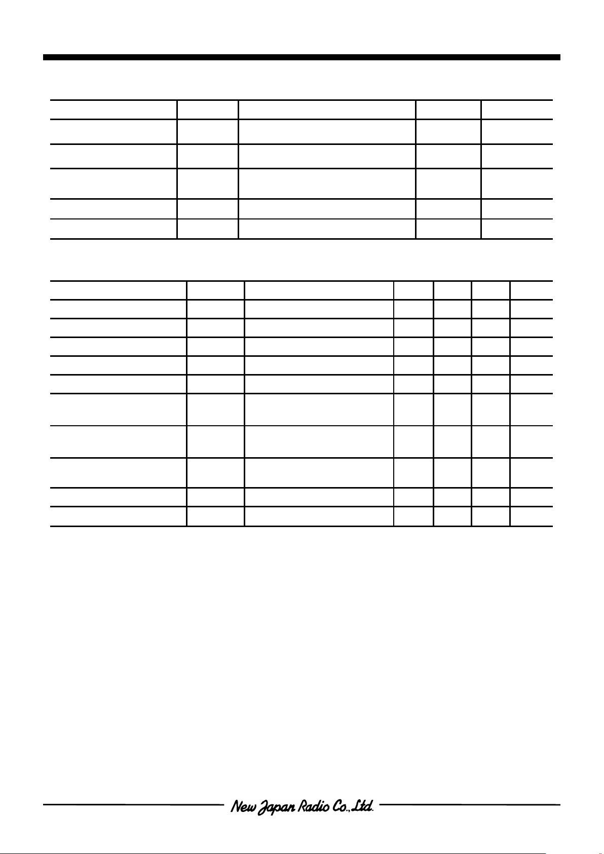
nPIN CONFIGURATION
nTRUTH TABLE
V
CTL1
H L L H
V
CTL2
L H L H
P1-PC ON OFF
Insertion Loss=13dB
P1 Return Loss=-3dB
Insertion Loss=13dB
P1 Return Loss=-2dB
P2-PC OFF ON
Insertion Loss=13dB
P2 Return Loss=-3dB
Insertion Loss=13dB
P2 Return Loss=-2dB
“H”=V
CTL (H),
“L”=V
CTL (L)
NOTE: The values of insertion losses and return losses are typical values at 2.0GHz.
NJG1517KB2
Pin Connection
1.P1
2.EXTCAP
3.P2
4.V
CTL2
5.PC
6.V
CTL1
KB2 Type
(Top view)
3
2
1
4
5
6
Orientation Mark
NJG1517KB2
- 2 -
n
ABSOLUTE MAXIMUM RATINGS
(Ta=25°C, ZS=Zl=50Ω)
PARAMETERS SYMBOL CONDITIONS RATINGS UNITS
Input Power P
in
V
CTL (L)
=0V, V
CTL (H)
=2.7V 28 dBm
Control Voltage V
CTL
V
CTL (H)
- V
CTL (L)
7.5 V
Power Dissipation P
D
19.4x14.0x0.2mm
FR4 Assembled Board, Tj=125°C
450 mW
Operating Temp. T
opr
-30~+85 °C
Storage Temp. T
stg
-55~+125 °C
n
ELECTRICAL CHARACTERISTICS
(V
CTL (L)
=0V, V
CTL (H)
=2.7V, ZS=Zl=50Ω, R1=560KΩ, C6=10pF, Ta=25°C)
PARAMETERS SYMBOL CONDITIONS MIN TYP MAX UNITS
Control voltage (Low) V
CTL (L)
-0.2 0 0.2 V
Control voltage (High) V
CTL (H)
2.5 2.7 6.5 V
Control current I
CTL
f=2.0GHz, Pin=10dBm - 5 6 uA
Insertion loss 1 LOSS1 f=1.0GHz, Pin=0dBm - 0.3 0.6 dB
Insertion loss 2 LOSS2 f=2.0GHz, Pin=0dBm - 0.5 0.8 dB
Isolation 1
(PC-P1, PC-P2, P1-P2)
ISL1 f=1.0GHz, Pin=0dBm 25 27 - dB
Isolation 2
(PC-P1, PC-P2, P1-P2)
ISL2
f=2.0GHz, Pin=0dBm,
C6=5pF
21 23 - dB
Pin at 1dB
compression point
P
-1dB
f=2.0GHz 20 23 - dBm
VSWR (PC, P1, P2) VSWR f=0.05~2.5GHz, ON State - 1.3 1.6
Switching time T
SW
f=0.05~2.5GHz - 15 - ns
* The control current ICTL depends on the resistance of R1. Smaller resistance of R1 make larger control current.
NJG1517KB2
- 3 -
n
TERMINAL INFORMATION
No. SYMBOL DESCRIPTIONS
1 P1
RF port. This port is connected with PC port by controlling 6th pin (V
CTL (H)
) to
2.5~6.5V and 4th pin(V
CTL(L)
) to -0.2~+0.2V. An external capacitor is required
to block the DC bias voltage of internal circuit. (50~100MHz: 0.01µF,
0.1~0.5GHz: 1000pF, 0.5~2.5GHz: 56pF)
2 EXTCAP
External capacitor terminal. The isolation characteristics depends on the
value of the capacitor which connected with GND. An external capacitor is
required to block the DC bias voltage of internal circuit. (50MHz~1.7GHz:
10pF, 1.7~2.5GHz: 5pF)
3 P2
RF port. This port is connected with PC port by controlling 4th pin(V
CTL(H)
) to
2.5 – 6.5V and 6th pin(V
CTL(L)
) to -0.2~+0.2V. In order to block the DC bias
voltage of internal circuit, an external capacitor is required. (50~100MHz:
0.01µF, 0.1~0.5GHz: 1000pF, 0.5~2.5GHz: 56pF)
4 V
CTL2
Control port 2. The voltage of this port controls PC to P2 state. The ‘ON’ and
‘OFF’ state is toggled by controlling voltage of this terminal such as highstate (2.5~6.5V) or low-state (-0.2~+0.2V). The voltage of 6th pin have to be
set to opposite state. The bypass capacitor has to be chosen to reduce
switching time delay from 10pF~1000pF range.
5 PC
Common RF port. In order to block the DC bias voltage of internal circuit, an
external capacitor is required. (50~100MHz: 0.01µF, 0.1~0.5GHz: 1000pF,
0.5~2.5GHz: 56pF)
6 V
CTL1
Control port 1. The voltage of this port controls PC to P2 state. The ‘ON’ and
‘OFF’ state is toggled by controlling voltage of this terminal such as highstate (2.5~6.5V) or low-state (-0.2~+0.2V). The voltage of 4th pin have to be
set to opposite state. The bypass capacitor has to be chosen to reduce
switching time delay from 10pF~1000pF range.
NJG1517KB2
- 4 -
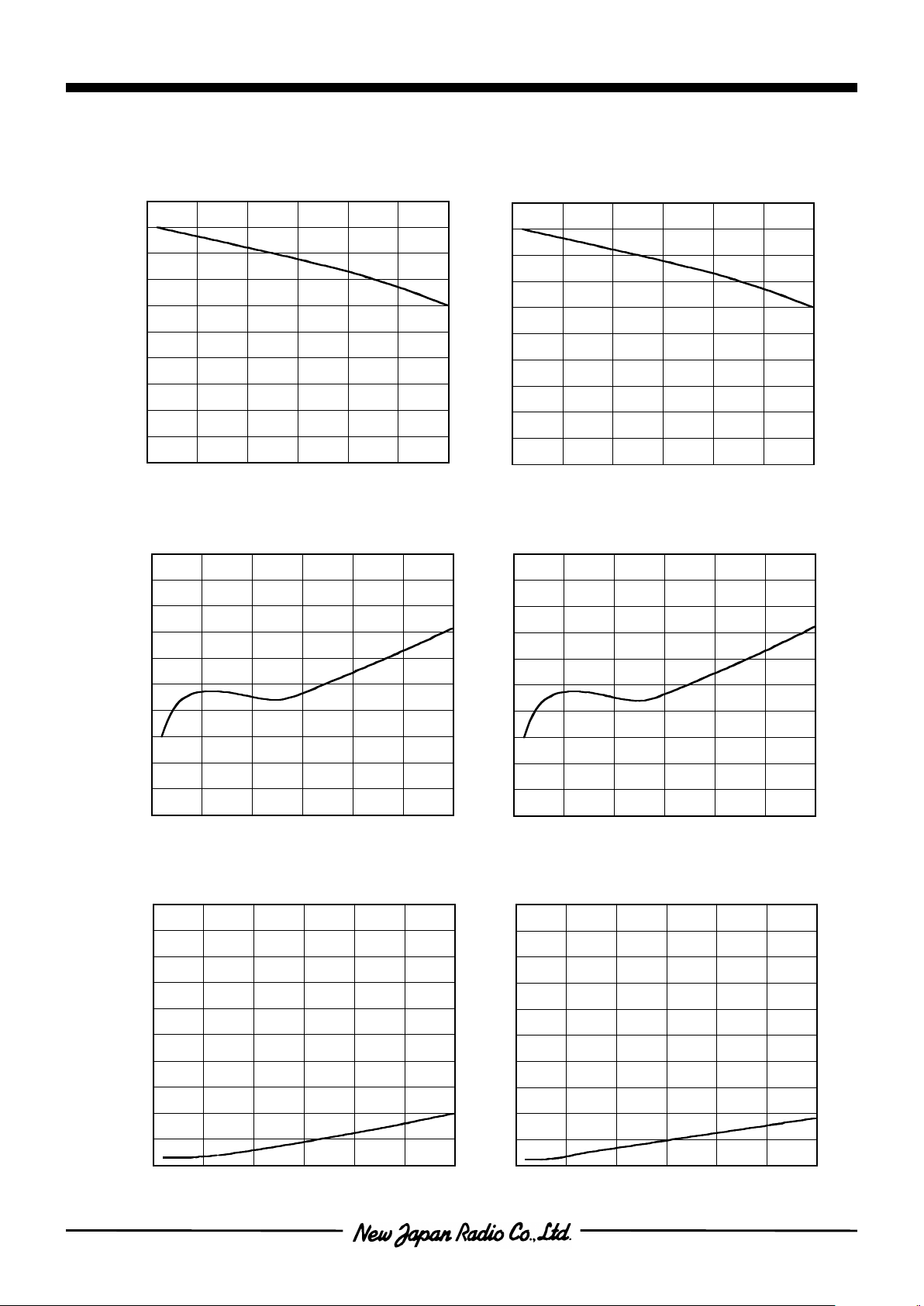
-2
-1.6
-1.2
-0.8
-0.4
0
0 0.5 1 1.5 2 2.5 3
Insertion Loss (dB)
Frequency (GHz)
PC-P1 Insertion Loss vs. Frequency
(V
CTL1
=2.7V,V
CTL2
=0V,Pin=0dBm)
-2
-1.6
-1.2
-0.8
-0.4
0
0 0.5 1 1.5 2 2.5 3
Insertion Loss (dB)
Frequency (GHz)
PC-P2 Insertion Loss vs. Frequency
(V
CTL1
=0V,V
CTL2
=2.7V,Pin=0dBm)
-50
-40
-30
-20
-10
0
0 0.5 1 1.5 2 2.5 3
Isolation (dB)
Frequency (GHz)
PC-P1 Isolation vs. Frequency
(V
CTL1
=0V,V
CTL2
=2.7V,Pin=0dBm)
-50
-40
-30
-20
-10
0
0 0.5 1 1.5 2 2.5 3
Isolation (dB)
Frequency (GHz)
PC-P2 Isolation vs. Frequency
(V
CTL1
=2.7V,V
CTL2
=0V,Pin=0dBm)
1
1.4
1.8
2.2
2.6
3
0 0.5 1 1.5 2 2.5 3
VSWR
Frequency (GHz)
PC-P1 VSWR vs. Frequency
(V
CTL1
=2.7V,V
CTL2
=0V,PC port)
1
1.4
1.8
2.2
2.6
3
0 0.5 1 1.5 2 2.5 3
VSWR
Frequency (GHz)
P1-PC VSWR vs. Frequency
(V
CTL1
=2.7V,V
CTL2
=0V,P1 port)
n
ELECTRICAL CHARACTERISTICS
(100MHz~3GHz, with application circuit, R1=560KΩ, C6=10pF, Losses of external circuit are excluded)
 Loading...