

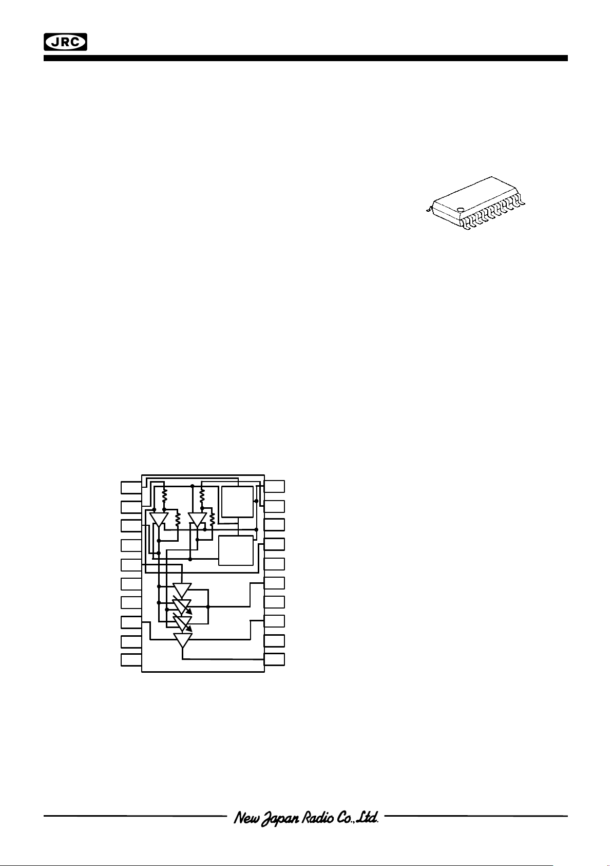
NJG1309VB2
- 1 -
TRANSMITTING POWER AMPLIFIER
GaAs MMIC
n
GENERAL DESCRIPTION
n
PACKAGE OUTLINE
NJG1309VB2 is a positive voltage supply type GaAs power
amplifier MMIC designed for Digital Cordless Phone.
Gate bias and Gain control bias terminals are supplied
by positive voltage.
These terminals have high-impedance characteristics.
NJG1309VB2 can reduce power
consumption at receiving mode by “Standby Function”.
n
FEATURES
lOperating frequency range f=1.9GHz typ.
lPositive voltage supply V
DD2,3
=+3.0V typ. +VGG=+1.0V typ.
lLow current consumption 150mA typ. @21dBm output power
lHigh gain 37dB typ. @21dBm output power
lGain control range 26dB typ. @21dBm output power
lPackage SSOP20-B2 (Pin pitch 0.5mm)
n
PIN CONFIGURATION
NJG1309VB2
CR
Oscillator
DC/DC
Converter
20
19
18
17
16
15
14
13
12
11
1
2
3
4
5
6
7
8
9
10
V Type
(Top View)
Pin Connection
1.V
STB
11.RF
out
2.+V
GG
12.GND
3.-V
GG1
13.V
DD3
4.GND 14.GND
5.RF
in
15V
DD2
6.GND 16.GND
7.GND 17.GND
8.-V
GG2
18.-V
CONT
9.GND 19.+V
CONT
10.GND 20.V
DD1
- 2 -
NJG1309VB2
n
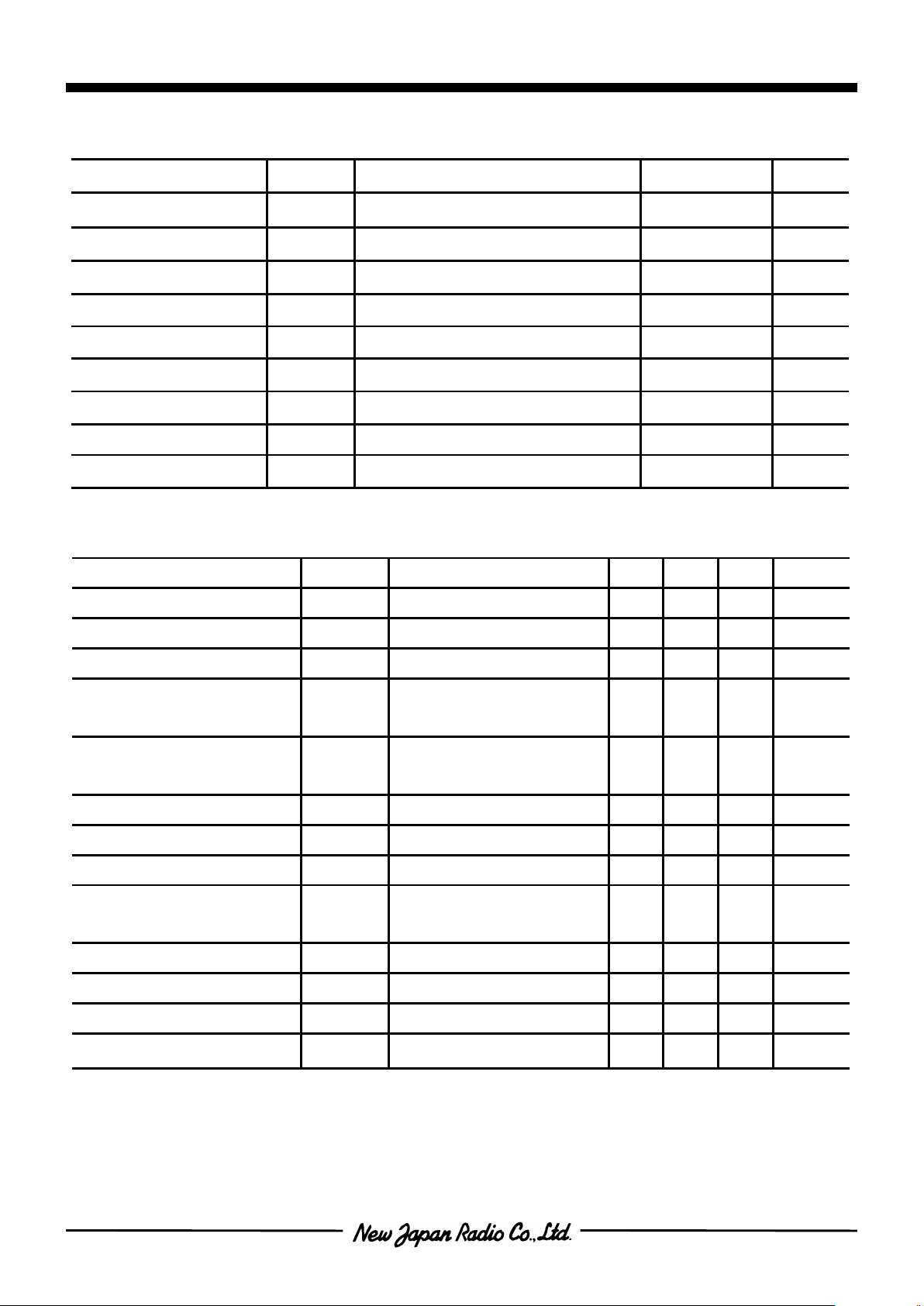
ABSOLUTE MAXIMUM RATINGS
(Zs=Zl=50Ω, Ta=25°C)
n
ELECTRICAL CHARACTERISTICS 1
(V
DD1
=3V,V
STB
=2.7V, +V
CONT
=0V, f=1.9GHz, Zs=Zl=50Ω, Ta=25°C)
PARAMETER SYMBOL CONDITIONS RATINGS UNITS
Drain Voltage 1 V
DD1
+VGG=1.0V 5.5 V
Drain Voltage 2 V
DD2,3
+VGG=1.0V 6.0 V
Gate Voltage +V
GG
V
DD2,3
=3.0V -0.5~V
DD1
+0.5 V
Gain Control Voltage +V
CONT
V
DD2,3
=3.0V -0.5~V
DD1
+0.5 V
Standby Voltage V
STB
-0.5~V
DD1
+0.5 V
Input Power P
in
V
DD2,3
=3.0V, +VGG=1.0V 3.0 dBm
Power Dissipation P
D
At on PCB board 600 mW
Operating Temperature T
opr
-40~+85 °C
Storage Temperature T
stg
-55~+150 °C
PARAMETER SYMBOL CONDITIONS MIN TYP MAX UNITS
Operating frequency freq V
DD2,3
=3.0V 1.85 1.90 1.95 GHz
Drain Voltage 1 V
DD1
2.7 3.0 5.2 V
Drain Voltage 2 V
DD2,3
2.9 3.0 5.2 V
Standby Terminal
Input Voltage (H)
V
STB
(H) 2.4 2.7 3.0 V
Standby Terminal
Input Voltage (L)
V
STB
(L) 0.0 0.0 0.6 V
Gain Control Voltage +V
CONT
0.0 - 2.0 V
Gate Voltage +V
GG
V
DD2,3
=3.0V, I
idle
=130mA 0.6 1.0 1.4 V
Idle Current *1 I
idle
V
DD2,3
=3.0V, RF OFF 125 130 135 mA
Operating Current *1 I
DD2,3
V
DD2,3
=3.0V,I
idle
=130mA
P
out
=21dBm
- 150 165 mA
V
DD1
Terminal Current(H) I
DD1
(H) V
DD2,3
=3V,P
out
=21dBm - 0.9 1.25 mA
V
DD1
Terminal Current(L) I
DD1
(L) V
STB
=0V,V
DD2,3
=0V - 0.5 1.0 uA
V
GG1
Terminal Current I
GG
+VGG=2.0V - 5 10 uA
+V
CONT
Terminal Current I
CONT
+V
CONT
=2.0V - 5 10 uA
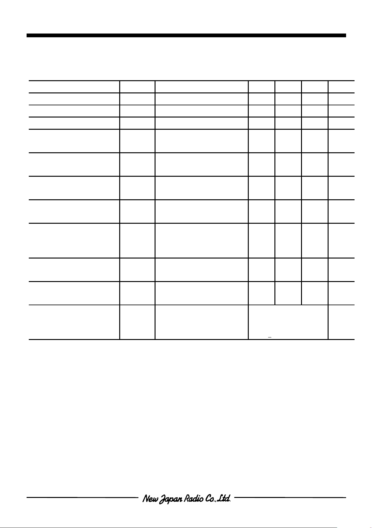
NJG1309VB2
- 3 -
n
ELECTRICAL CHARACTERISTICS 1
(V
DD1
=3V, V
STB
=2.7V, +V
CONT
=0V, f=1.9GHz, Zs=Zl=50Ω, Ta=25°C)
*1: Total current of V
DD2
terminal and V
DD3
terminal.
*2: Timing chart of input terminal voltage is mentioned in the separate sheet of paper.
PARAMETER SYMBOL CONDITIONS MIN TYP MAX UNIT
V
STB
Terminal Current I
STB
- 0.5 1.0 uA
-VGG,-V
CONT
Rise Time*2 TRDD 0.01uF Load Capacitance - - 400 uSEC
-VGG,-V
CONT
Fall Time*2 T
STB
- - 20 mSEC
+VGG Terminal Input
Resistance
R1 300 500 700 kΩ
+V
CONT
Terminal Input
Resistance
R2 300 500 700 kΩ
Power Gain Gain
V
DD2,3
=3.0V, I
idle
=130mA
P
out
=21dBm
34 37 40 dB
Gain Flatness G
flat
V
DD2,3
=3.0V, I
idle
=130mA
P
out
=21dBm
- 1.0 1.5 dB
Gain Control Range G
cont
V
DD2,3
=3.0V, I
idle
=130mA
P
out
=21dBm
+V
CONT
=0.0 to 2.0V
21 26 31 dB
Pout at 1dB Gain
Compression point
P
-1dB
V
DD2,3
=3.0V, I
idle
=130mA - 21 - dBm
Harmonics P
hm
V
DD2,3
=3.0V, I
idle
=130mA
P
out
=21dBm
- -40 -30 dBc
Load VSWR tolerance -
V
DD2,3
=3.0V, I
idle
=130mA
P
out
=21dBm,
Load VSWR=1:4 All Phase
Parasitic oscillation
for fundamental signal
level: -60dBc
-
≤
- 4 -
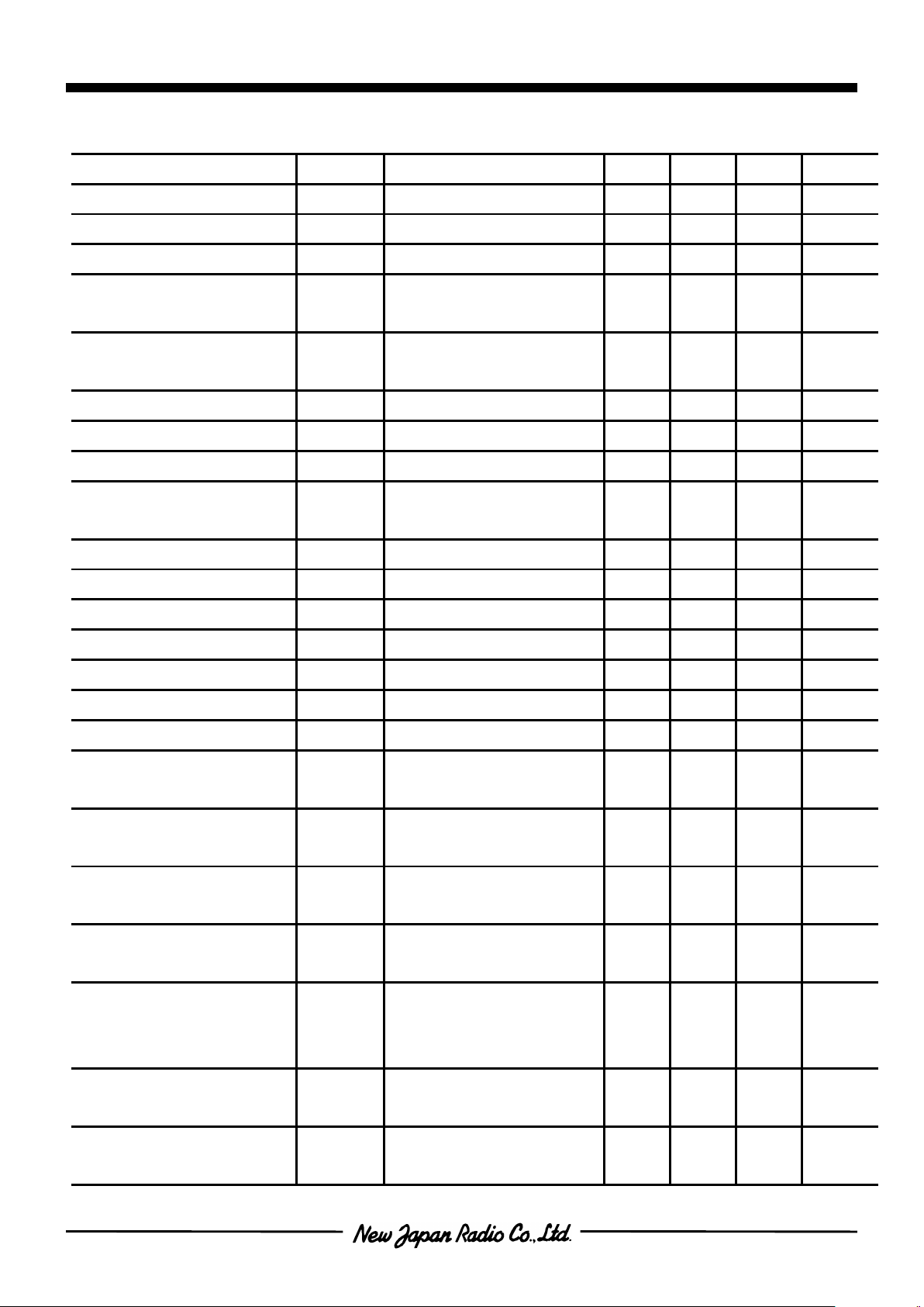
NJG1309VB2
n
ELECTRICAL CHARACTERISTICS 2
(V
DD1
=3V, V
STB
=2.7V, +V
CONT
=0V, f=1.765GHz, Zs=Zl=50Ω, Ta=25°C)
PARAMETER SYMBOL CONDITIONS MIN TYP MAX UNITS
Operating frequency freq V
DD2,3
=3.0V 1.750 1.765 1.780 GHz
Drain Voltage 1 V
DD1
2.7 3.0 5.2 V
Drain Voltage 2 V
DD2,3
2.9 3.0 5.2 V
Standby Terminal
Input Voltage (H)
V
STB
(H) 2.4 2.7 3.0 V
Standby Terminal
Input Voltage (L)
V
STB
(L) 0.0 0.0 0.6 V
Gain Control Voltage +V
CONT
0.0 - 2.0 V
Gate Voltage +V
GG
V
DD2,3
=3.0V, I
idle
=130mA 0.6 1.0 1.4 V
Idle Current *1 I
idle
V
DD2,3
=3.0V, RF OFF 125 130 135 mA
Operating Current *1 I
DD2,3
V
DD2,3
=3.0V,I
idle
=130mA
P
out
=21dBm
- 155 - mA
V
DD1
Terminal Current(H) I
DD1
(H) V
DD2,3
=3V,P
out
=21dBm - 0.9 - mA
V
DD1
Terminal Current(L) I
DD1
(L) V
STB
=0V,V
DD2,3
=0V - 0.5 - uA
VGG Terminal Current I
GG
+VGG=2.0V - 5 - uA
+V
CONT
Terminal Current I
CONT
+V
CONT
=2.0V - 5 - uA
V
STB
Terminal Current I
STB
- 0.5 - uA
-VGG,-V
CONT
Rise Time*2 TRDD 0.01uF Load Capacitance - - 400 uSEC
-VGG,-V
CONT
Fall Time*2 T
STB
- - 20 mSEC
+VGG Terminal Input
Resistance
R1 300 500 700 kΩ
+V
CONT
Terminal Input
Resistance
R2 300 500 700 kΩ
Power Gain Gain
V
DD2,3
=3.0V, I
idle
=130mA
P
out
=21dBm
- 36 - dB
Gain Flatness G
flat
V
DD2,3
=3.0V, I
idle
=130mA
P
out
=21dBm
- 0.5 - dB
Gain Control Range G
cont
V
DD2,3
=3.0V, I
idle
=130mA
P
out
=21dBm
+V
CONT
=0.0 to 2.0V
- 25 - dB
Output Power at
1dB Compression point
P
-1dB
V
DD2,3
=3.0V, I
idle
=130mA - 20 - dBm
Harmonics P
hm
V
DD2,3
=3.0V, I
idle
=130mA
P
out
=21dBm
- -40 - dBc
NJG1309VB2
- 5 -
n
ELECTRICAL CHARACTERISTICS 2
(V
DD1
=3V, V
STB
=2.7V, +V
CONT
=0V, f=1.765GHz, Zs=Zl=50Ω, Ta=25°C)
*1:Total current of V
DD2
terminal and V
DD3
terminal.
*2:Timing chart of input terminal voltage is mentioned in the separate sheet of paper.
PARAMETER SYMBOL CONDITIONS MIN TYP MAX UNITS
Load VSWR tolerance -
V
DD2,3
=3.0V, I
idle
=130mA
P
out
=21dBm,
Load VSWR=1:4 All Phase
Parasitic oscillation
for fundamental signal
level: -60dBc
-
≤
- 6 -
NJG1309VB2
n
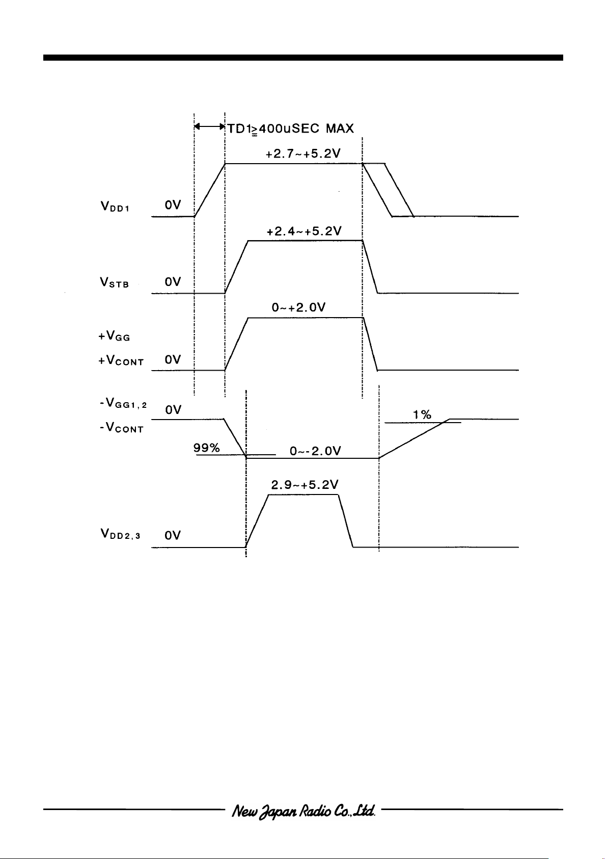
TIMING CHART
1) Timing chart of setting and shut of supply voltage and control voltage, V
DD1
, +V
GG
,and V
CONT
.
Notes
(1) To prevent latch-up, V
DD1
should be more than V
STB
,+VGG and +V
CONT
.
(2) The rising time of VDD1 is 400uSEC.maximum in case of the recommended circuit.

NJG1309VB2
- 7 -
n
TIMING CHART
2) Timing chart of burst operation using V
STB
.

- 8 -
NJG1309VB2
n
TERMINAL INFORMATION
TERMINAL INFORMATION
PIN No. SYMBOL DESCRIPTIONS
1 V
STB
The output voltage of DC/DC converter is toggled ON/OFF by changing voltage to
this terminal to High/Low.
2 +V
GG
The positive voltage of this terminal is supplied to op-amp 1 in the DC/DC
converter, and its output voltage (negative) is internally supplied to the gate ports
of #1 to 3 amplifiers. The current of amplifier is controlled by the voltage of this
terminal.
3 -V
GG1
The voltage of the gate ports of #1 to 3 amplifier are supplied through this
terminal. Please place a capacitor at this terminal as close as possible.
4 GND Ground terminal(0V)
5 RF
in
This terminal is a signal input terminal connected to input port of amplifier through
matching circuit and DC blocking capacitor.
6 GND Ground terminal(0V)
7 GND Ground terminal(0V)
8 -V
GG2
This terminal is Connected to gate fourth stage amplifier. Please connect with V
GG2
terminal on PCB board and place a bypass possible , since this terminal is
NOT connected with op-amp input.
9 GND Ground terminal(0V)
10 GND Ground terminal(0V)
11 RF
out
This terminal is a signal output terminal connected to the output port of amplifier
through matching circuit and DC blocking capacitor.
12 GND Ground terminal(0V)
13 V
DD3
This terminal is connected to drain port of fourth stage amplifier. Please place a
choke inducter and a bypass capacitor shown in the application circuit below.
14 GND Ground terminal(0V)
15 V
DD2
The voltage of the gate ports of #1 to 3 amplifier are supplied through this
terminal. Please place a capacitor at this terminal as close as possible.
16 GND Ground terminal(0V)
17 GND Ground terminal(0V)
18 -V
CONT
This terminal is a gain control terminal of amplifier, and also internally connected
to output port of op-amp2. Please place a bypass capacitor at this terminal shown
in the application circuit below as close as possible.
19 +V
CONT
The positive voltage of this terminal is supplied to op-amp2 in the DC/Dc
converter, and its output voltage(negative) is internally supplied to the gain
control port of amplifier. The gain of amplifier is controlled by the voltage of this
terminal.
20 V
DD1
This terminal is a voltage supply terminal of DC/DC converter. Please place
bypass capacitor shown in the application circuit below as close as possible.
NOTE 1) The ground terminal(4,6,7,9,10,12,14,16,17)shond be directly connected to ground plane
To minimize fringing inductance.

NJG1309VB2
- 9 -
n
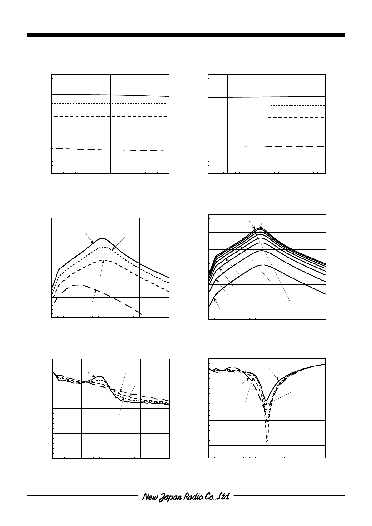
TYPICAL CHARACTERISTICS
Timing Chart 1 (+VGG: DC, X-axis: 1msec/div) Timing Chart 2 (+VGG: DC, X-axis: 100usec/div)
V
DD1
=3Vdc, +VGG=1Vdc, +V
CONT
=0V V
DD1
=3Vdc, +VGG=1Vdc, +V
CONT
=0V
V
STB
: V0-p=3V, Period=5msec, Duty=50% V
STB
: V0-p=3V, Period=5msec, Duty=50%
Timing Chart 3(+VGG: Pulse, X-axis: 1msec/div) Timing Chart 4(+VGG: Pulse, X-axis: 100usec/div)
V
DD1
=3Vdc, +V
CONT
=0V V
DD1
=3Vdc, +V
CONT
=0V
+VGG: V0-p=1V, Period=5msec, Duty=50% +VGG: V0-p=1V, Period=5msec, Duty=50%
V
STB
: V0-p=3V, Period=5msec, Duty=50% V
STB
: V0-p=3V, Period=5msec, Duty=50%
Real vertical voltage scale should be ten times higher than the scale indicated under each graph,
because 1:10 probes are used on all of Ch1, Ch2 and Ch3.
- 10 -
NJG1309VB2
0
10
20
30
40
50
1.85 1.90 1.95
Small Signal Power Gain [ dB ]
Freq [ GHz ]
Small Signal Power Gain vs. Frequency
V
DD1=VSTB=VDD2,3
=3V,I
DD2,3
=130mA at Ta=25oC
+V
CONT
=0.0V
+V
CONT
=0.9V
+V
CONT
=1.1V
+V
CONT
=2.0V
n
TYPICAL CHARACTERISTICS
-20
-15
-10
-5
0
1.0 1.5 2.0 2.5 3.0
Input Return Loss [ dB ]
Freq [ GHz ]
Intput Return Loss vs. Frequency
V
DD1=VSTB=VDD2,3
=3V,I
DD2,3
=130mA at Ta=25oC
+V
CONT
=0.0V
+V
CONT
=0.9V
+V
CONT
=2.0V
+V
CONT
=1.1V
0
10
20
30
40
50
1.0 1.5 2.0 2.5 3.0
Small Signal Power Gain [ dB ]
Freq [ GHz ]
Small Signal Power Gain vs. Frequency
V
DD1=VSTB=VDD2,3
=3V,I
DD2,3
=130mA at Ta=25oC
+V
CONT
=0.0V
+V
CONT
=0.9V
+V
CONT
=2.0V
+V
CONT
=1.1V
-10
0
10
20
30
40
50
1.0 1.5 2.0 2.5 3.0
Small Siganl Power Gain [ dB ]
Freq [ GHz ]
Small Signal Power Gain vs. Frequency
V
DD1=VSTB=VDD2,3
=3V,+V
CONT
=0V at Ta=25oC
I
DD2,3
=20mA
I
DD2,3
=160mA
I
DD2,3
=40mA
I
DD2,3
=60mA
I
DD2,3
=80mA
I
DD2,3
=140mA
I
DD2,3
=100mA
I
DD2,3
=120mA
-40
-35
-30
-25
-20
-15
-10
-5
0
1.0 1.5 2.0 2.5 3.0
Output Return Loss [ dB ]
Freq [ GHz ]
Output Return Loss vs. Frequency
V
DD1=VSTB=VDD2,3
=3V,I
DD2,3
=130mA at Ta=25oC
+V
CONT
=0.0V
+V
CONT
=0.9V
+V
CONT
=2.0V
+V
CONT
=1.1V
0
10
20
30
40
50
1.750 1.755 1.760 1.765 1.770 1.775 1.780
Small Signal Power Gain [ dB ]
Freq [ GHz ]
Small Signal Power Gain vs. Frequency
V
DD1=VSTB=VDD2,3
=3V,I
DD2,3
=130mA at Ta=25oC
+V
CONT
=0.0V
+V
CONT
=0.9V
+V
CONT
=1.1V
+V
CONT
=2.0V

NJG1309VB2
- 11 -
8
10
12
14
16
18
20
22
24
5
10
15
20
25
30
35
40
45
-30 -25 -20 -15 -10 -5 0 5
Output Power [ dBm ]
Gain:Power Gain [ dB ]
Input Power [ dBm ]
V
DD1=VSTB=VDD2,3
=3V,I
idle
=130mA,f=1.9GHz at Ta=25oC
Output Power,Gain vs. Input Power
+V
CONT
=0.0V
0.9V
1.1V
+V
CONT
=0.0V
0.9V
1.1V
8
10
12
14
16
18
20
22
24
100
120
140
160
180
200
220
240
260
-30 -25 -20 -15 -10 -5 0 5
Output Power [ dBm ]
I
DD2,3
:Operation Current at V
DD2,3
[ mA ]
Input Power [ dBm ]
V
DD1=VSTB=VDD2,3
=3V,I
idle
=130mA,f=1.9GHz at Ta=25oC
Output Power,IDD2,3 vs. Input Power
+V
CONT
=0.0V
0.9V
1.1V
+V
CONT
=0.0V
0.9V
1.1V
8
10
12
14
16
18
20
22
24
0
10
20
30
40
50
60
70
80
-30 -25 -20 -15 -10 -5 0 5
Output Power [ dBm ]
PAE:Power Added Efficiency [ % ]
Input Power [ dBm ]
V
DD1=VSTB=VDD2,3
=3V,I
idle
=130mA,f=1.9GHz at Ta=25oC
Output Power,PAE vs. Input Power
+V
CONT
=0.0V
0.9V
1.1V
+V
CONT
=0.0V
0.9V
1.1V
8
10
12
14
16
18
20
22
24
5
10
15
20
25
30
35
40
45
-30 -25 -20 -15 -10 -5 0 5 10
Output Power [ dBm ]
Gain:Power Gain [ dB ]
Input Power [ dBm ]
V
DD1=VSTB=VDD2,3
=3V,I
idle
=130mA,f=1.765GHz at Ta=25oC
Output Power,Gain vs. Input Power
+V
CONT
=0.0V 0.9V
1.1V
+V
CONT
=0.0V
0.9V
1.1V
8
10
12
14
16
18
20
22
24
100
120
140
160
180
200
220
240
260
-30 -25 -20 -15 -10 -5 0 5 10
Output Power [ dBm ]
Input Power [ dBm ]
V
DD1=VSTB=VDD2,3
=3V,I
idle
=130mA,f=1.765GHz at Ta=25oC
Output Power,IDD2,3 vs. Input Power
+V
CONT
=0.0V 0.9V
1.1V
+V
CONT
=0.0V
0.9V
1.1V
I
DD2,3
:Operation Current at V
DD2,3
[ mA ]
8
10
12
14
16
18
20
22
24
0
10
20
30
40
50
60
70
80
-30 -25 -20 -15 -10 -5 0 5 10
Output Power [ dBm ]
Input Power [ dBm ]
V
DD1=VSTB=VDD2,3
=3V,I
idle
=130mA,f=1.765GHz at Ta=25oC
+V
CONT
=0.0V 0.9V
1.1V
+V
CONT
=0.0V
0.9V
1.1V
PAE:Power Added Efficiency [ % ]
Output Power,PAE vs. Input Power
n
TYPICAL CHARACTERISTICS

- 12 -
NJG1309VB2
140
145
150
155
160
165
170
175
180
90 100 110 120 130 140 150 160 170
I
DD2,3
:Operation Current at V
DD2,3
[ mA ]
Iidle:Idle Current at V
DD2,3
(RF OFF) [ mA ]
V
DD1=VSTB=VDD2,3
=3.0V,+V
CONT
=0V
IDD2,3 vs. Iidle
f=1.9GHz,P
out
=21dBm Ta=25oC
V
DD2,3
=2.9V
V
DD2,3
=3.0V
V
DD2,3
=3.5V
V
DD2,3
=5.2V
V
DD2,3
=4.0V
36
37
38
39
40
41
42
43
44
140
145
150
155
160
-50 0 50 100
Gain:Power Gain [ dB ]
I
DD2,3
:Operation Current at V
DD2,3
[ mA ]
V
DD1=VSTB=VDD2,3
=3V,+V
CONT
=0V,I
idle
=130mA
Gain,IDD2,3 vs. Ta
Ta:Ambient Temperature [ oC ]
f=1.9GHz,P
out
=21dBm at Ta=25oC
0.82
0.84
0.86
0.88
0.90
0.92
1.6
1.8
2.0
2.2
2.4
2.6
-50 0 50 100
I
DD1
:Operation Current at V
DD1
[ mA ]
I
GG
:Operation Current at +V
GG
[ uA ]
V
DD1=VSTB=VDD2,3
=3V,+V
CONT
=0V,I
idle
=130mA
IDD1,IGG vs. Ta
Ta:Ambient Temperature [ oC ]
f=1.9GHz,P
out
=21dBm at Ta=25oC
20
25
30
35
40
0
5
10
15
20
0.0 0.2 0.4 0.6 0.8 1.0 1.2 1.4
Gain:Power Gain [ dB ]
G
CONT
:Variable Gain [ dB ]
+V
CONT
:Gain Controlled Voltage [ V ]
V
DD1=VSTB=VDD2,3
=3V,I
idle
=130mA
Gain,GCONT vs. +VCONT
f=1.9GHz,P
out
=21dBm at Ta=25oC
20
25
30
35
40
0
5
10
15
20
0.0 0.2 0.4 0.6 0.8 1.0 1.2 1.4
Gain:Power Gain [ dB ]
G
CONT
:Variable Gain [ dB ]
+V
CONT
:Gain Controlled Voltage [ V ]
V
DD1=VSTB=VDD2,3
=3V,I
idle
=130mA
Gain,GCONT vs. +VCONT
f=1.765GHz,P
out
=21dBm at Ta=25oC
n
TYPICAL CHARACTERISTICS
34
36
38
40
42
44
90 100 110 120 130 140 150 160 170
Gain:Power Gain [ dB ]
Iidle:Idle Current at V
DD2,3
(RF OFF) [ mA ]
V
DD1=VSTB=VDD2,3
=3.0V,+V
CONT
=0V
Gain vs. Iidle
f=1.9GHz,P
out
=21dBm Ta=25oC
VDD
2,3
=4.0V
3.5V
3.0V
5.2V
2.9V

NJG1309VB2
- 13 -
n
TYPICAL CHARACTERISTICS
V
DD1=VSTB=VDD2,3
=3V,I
idle
=130mA
Harmonics Spectrum
+V
CONT
=0V,freq=1.9GHz,P
out
=21dB
V
DD1=VSTB=VDD2,3
=3V,I
idle
=130mA
+V
CONT
=0V,freq=1.9GHz,P
out
=21d
1.9GHz Band Spectrum

- 14 -
NJG1309VB2
n
TYPICAL CHARACTERISTICS
Scattering Parameters
V
DD1=VSTB=VDD2,3
=3.0V, I
DD2,3
=130mA, +V
CONT
=0.0

NJG1309VB2
- 15 -
n
RECOMMENDED CIRCUIT
(Top View)

- 16 -
NJG1309VB2
n
RECOMMENDED PCB DESIGN
(Top View)
PCB
FR-4
t=0.2mm
PCB Size
17.5mmX17.0mm
Microstrip Line Width
w=0.4mm(Zo=50Ω,
RFin and RFout port)
V
STB
+V
GG
V
DD1
+V
CONT
V
DD2,3
RF
in
RF
out
C2
C6
C5
C9
C8
L2
C4
C10
C12
C11
C1
C3
C7
Notes
[1] CMOS IC negative voltage generator has Internal CR oscillator, therefor to reduction of noise,
decoupling capacitor(C12) should be connected between the 20pin and the GND.
[2] Chip parts as follows should be connected to the leads of IC as near as possible.
(1) 3pin - C1
(2) 8pin - C2
(3) 13pin - L1
(4) 15pin - C3
[3] Chip parts list
Parts ID Constant Note
C1~C4 30pF MURATA GRM36 Series
C5~C8 1000pF MURATA GRM36 Series
C9~C11 0.01uF MURATA GRM39 Series
C12 1uF MURATA GRM39 Series
L2 10nH
TAIYO-YUDEN HK1608

NJG1309VB2
- 17 -
nPACKAGE OUTLINE (SSOP20-B2)
Lead material : Copper
Lead surface finish : Solder plating
Molding material : Epoxy resin
UNIT : mm
Weight : 66mg
Cautions on using this product
This product contains Gallium-Arsenide (GaAs) which is a harmful material.
• Do NOT eat or put into mouth.
• Do NOT dispose in fire or break up this product.
• Do NOT chemically make gas or powder with this product.
• To waste this product, please obey the relating law of your country.
This product may be damaged with electric static discharge (ESD) or spike voltage. Please handle
with care to avoid these damages.
[CAUTION]
The specifications on this databook are only
given for information , without any guarantee
as regards either mistakes or omissions. The
application circuits in this databook are
described only to show representative
usages
of the product and not intended for the
guarantee or permission of any right including
the industrial rights.
 Loading...