

A
查询NJL21V360A-M供应商
NJL21H/21V/22H/23H/24H000
INFRARED REMOTE CONTROL RECEIVER
GENERAL DESCRIPTION
The NJL21H/21V/22H/23H/24H000A series are small and high performance receiving devices for infrared
remote control system. They can operate under low and wide supply voltage (2.7V to 5.5V) with enhanced
5.4mm
5.7mm
5.4mm
8mm
6.3mm
11mm
15mm
6.3mm
immunity against the disturbance light.
FEATURES
1. Wide and low supply voltage 2.7V to 5.5V
2. Low supply current 0.43mA typ. Vcc=3.3V
3. Mold type and metal case type to meet the design of front panel.
4. Line-up for various center carrier frequencies.
APPLICATIONS
1. AV instruments such as Audio, TV, VCR, CD, MD, DVD, STB etc.
2. Home application such as Air-conditioner, Fan etc.
3. Game machine, toy etc.
LINE-UP
Mold type
View Top Top Side
Height
Carrier
Frequency
Fo= 36 kHz NJL21H360A NJL21H360AF3 NJL21V360A
36.7 kHz NJL21H367A NJL21H367AF3 NJL21V367A
38 kHz NJL21H380A NJL21H380AF3 NJL21V380A
40 kHz NJL21H400A NJL21H400AF3 NJL21V400A
Metal Case type
View Top Side
Height
Carrier
Frequency
Fo= 36 kHz NJL21H360A-M NJL22H360A NJL23H360A NJL24H360A NJL21V360A-M
36.7 kHz NJL21H367A-M NJL22H367A NJL23H367A NJL24H367A NJL21V367A-M
38 kHz NJL21H380A-M NJL22H380A NJL23H380A NJL24H380A NJL21V380A-M
40 kHz NJL21H400A-M NJL22H400A NJL23H400A NJL24H400A NJL21V400A-M
Regarding other frequency or packages, please contact to New JRC individually.
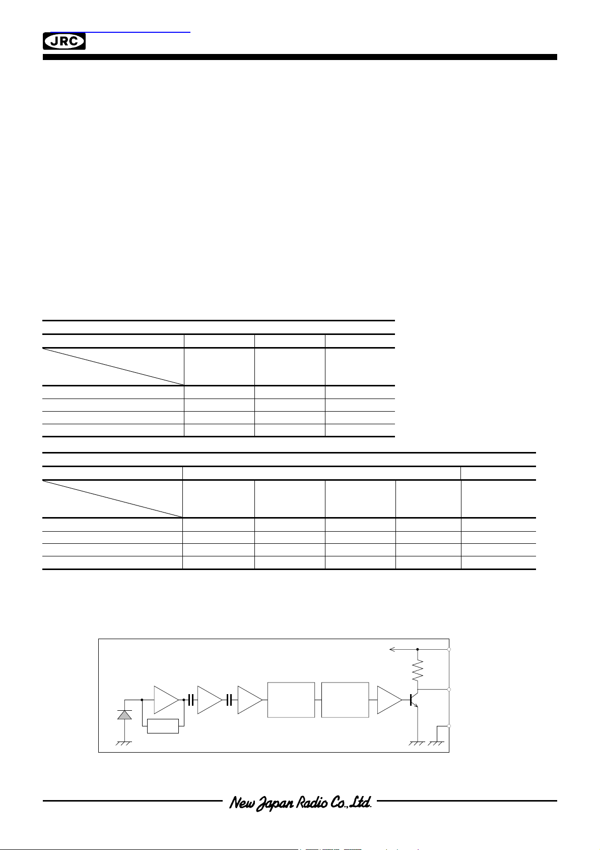
BLOCK DIAGRAM
Vcc
Head Amp 2nd Amp 3rd Amp
B.P.F .
PD
ABLC
Detec tor
Comparator
22K
Vout
GND

A
NJL21H/21V/22H/23H/24H000
ABSOLUTE MAXIMUM RATINGS (Ta=25°C)
PARAMETER SYMBOL RATINGS UNIT
Supply Voltage Vcc
Operating Temperature Range Topr
Storage Temperature Range Tstg -40 to +85 °C
Soldering Temperature Tsol 260 (5sec. 4.0mm from mold body) °C
RECOMMENDED OPERATING CONDITION
Supply Voltage Range Vcc 2.7 V to 5.5V
ELECTRO-OPTICAL CHARACTERISTICS (Vcc=3.3V, Ta=25°C)
PARAMETER SYMBOL TEST CONDITION MIN TYP MAX UNIT
Supply Current Icc No Signal Input
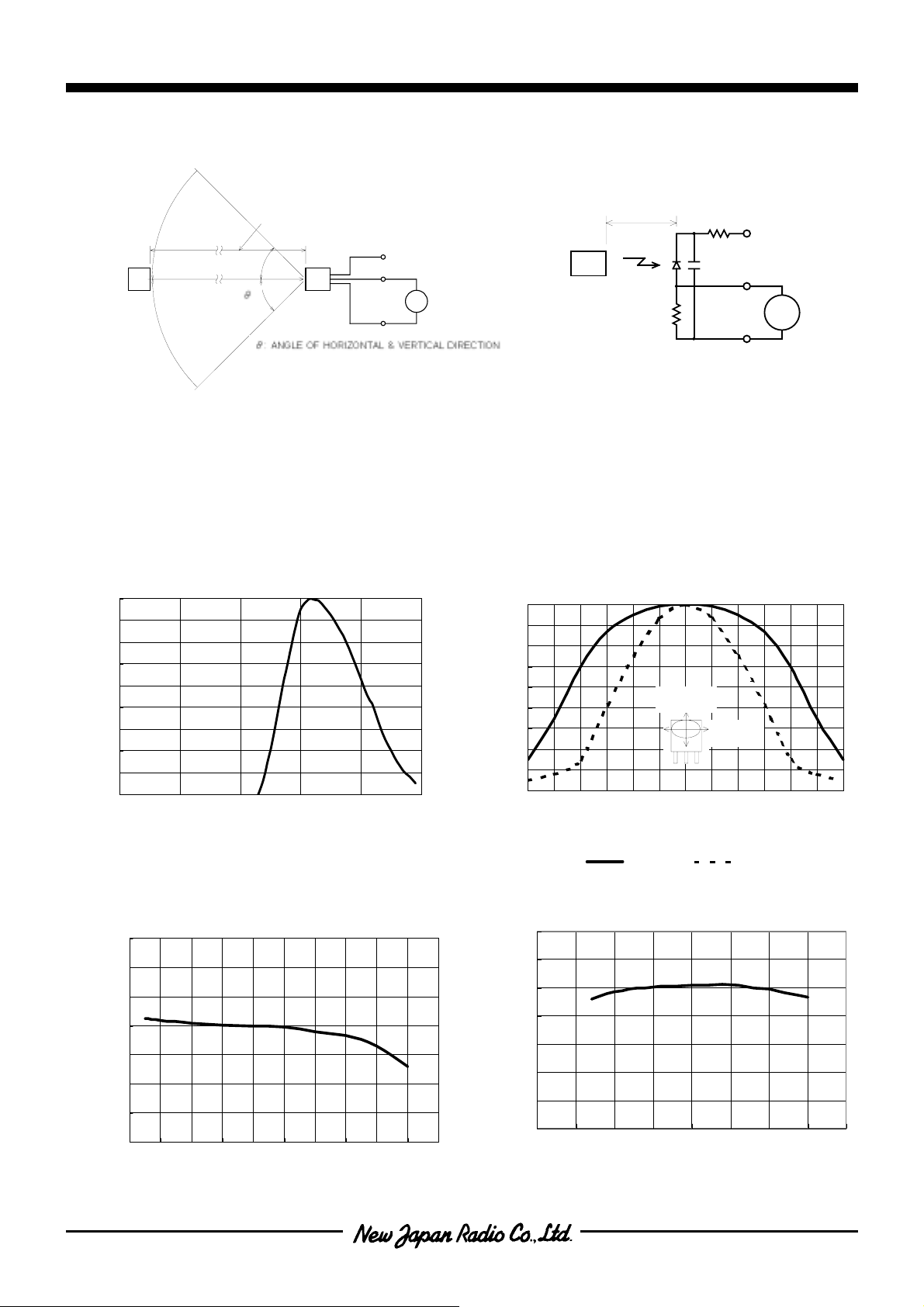
Transmission Distance Lc
Directivity
θL Angle of half Lc, Horizontal *2 *3
θV Angle of half Lc, Vertical *2 *3
Direction of Ray Axis *1 13 18
Output Voltage Low VL No Load
Output Voltage High VH No Load
Low Level Pulse Width TwL See Test Circuit
High Level Pulse Width TwH See Test Circuit
Center carrier Frequency fo See Line-up
Note *1:Test with each center carrier frequency under the test condition shown below.
*2:Place major axis of elliptic lens in horizontal direction and minor vertical.
*3:Four types of frequency :36.0, 36.7, 38.0, 40.0KHz
TEST METHOD
Test condition is as follows:
(1) Standard transmitter:
Transmitting waveform is shown in Fig.1
Transmitting power should be adjusted
so that output voltage Vout will be
400mVp-p.(Test circuit is shown in Fig.2)
Regarding IR LED used for transmitter,
λp=940nm, ∆λ=50nm.
Regarding photo diode,
Sensitivity S=26nA/Lx
in case light source temperature2856°K,
Ee=100Lx, VR=5V
6.3 V
-30 to +85 °C
— 0.43
0.56 mA
—
—
—
—
45
30
0.2
—
—
0.5
2.8 — —
400 — 850
350 — 800
—
*3
—
Carrier f requency i s adj usted t o
center f requency of each pr oduct
IR TRANSMITTER
OUTPUT WAVE FORM
600us
T
WH
OUTPUT PULSE
OF DEVICE
600us
T
WL
Fig.1 TRANSMITTER WAVE FORM
m
deg
deg
V
V
µs
µs
kHz
V
H
V
L
A
y
NJL21H/21V/22H/23H/24H000
(2) Test system: Shown in Fig.3.
STANDARD
TRANSMITTER
SENSING DISTANCE : L
Vcc
OUT
Vout
GND
Fig.3 TEST SYSTEM
Fig.2 STD.TRANSMITTER TEST CIRCUIT
TYPICAL CHARACTERISTICS
1.0
0.9
0.8
0.7
0.6
0.5
0.4
0.3
Relative Responsibirit
0.2
0.1
600 700 800 900 1000 1100
Spectral Response
(Ta=25°C )
Wavelength (nm)
1.0
0.9
0.8
0.7
0.6
0.5
0.4
0.3
0.2
Relative Transmission Distance
0.1
-60-50-40-30-20-10 0 102030405060
1000
900
800
700
600
500
400
Output Pulse Width TwL (µs)
300
0 2 4 6 8 10 12 14 16 18 20
Output Pulse Width vs. Distance
(Input Pulse Width=600µs, Vcc=3.3V, Ta=25°C)
Transmission Distance Lc (m)
Relative Transmission Distance
1.2
1.1
1.0
0.9
0.8
0.7
0.6
0.5
Transmission Dis tanc e vs. Supply Voltage
2.0 2.5 3.0 3.5 4.0 4.5 5.0 5.5 6.0
20cm
100K
(Ta=25°C)
Angle θ (deg)
Horizontal Vertical
Supply Voltage Vcc (V)
10K
+
-
Directivity
Vertical
(Ta=25°C)
4.9to5.1V
Horizontal
Vout

A
e
1.0
Transmission Distance vs. Carrier Frequency
(Vcc=3.3V, Ta=25°C)
0.9
0.8
0.7
0.6
Relativ e Transmission Distanc
0.5
24 26 28 30 32 34 36 38 40 42 44 46 48 50
Carrier Frequency (kHz)
fo=36kHz fo=38KHz fo=40KHz
RECOMMENDED APPLICATION CIRCUIT
NJL21H/21V/22H/23H/24H000
Transmission Distance vs. Temperature
(Vcc=3.3V)
1.2
1.1
1.0
0.9
0.8
0.7
0.6
Relative Transmission Distance
0.5
-40 -20 0 20 40 60 80 100
Ambient temperature Ta(°C)
1:OUT
2:GND
3:Vcc
47
47uF
Ω
Vcc
3
2
1
RC Filter should be connected closely between Vcc pin and GND pin.
A
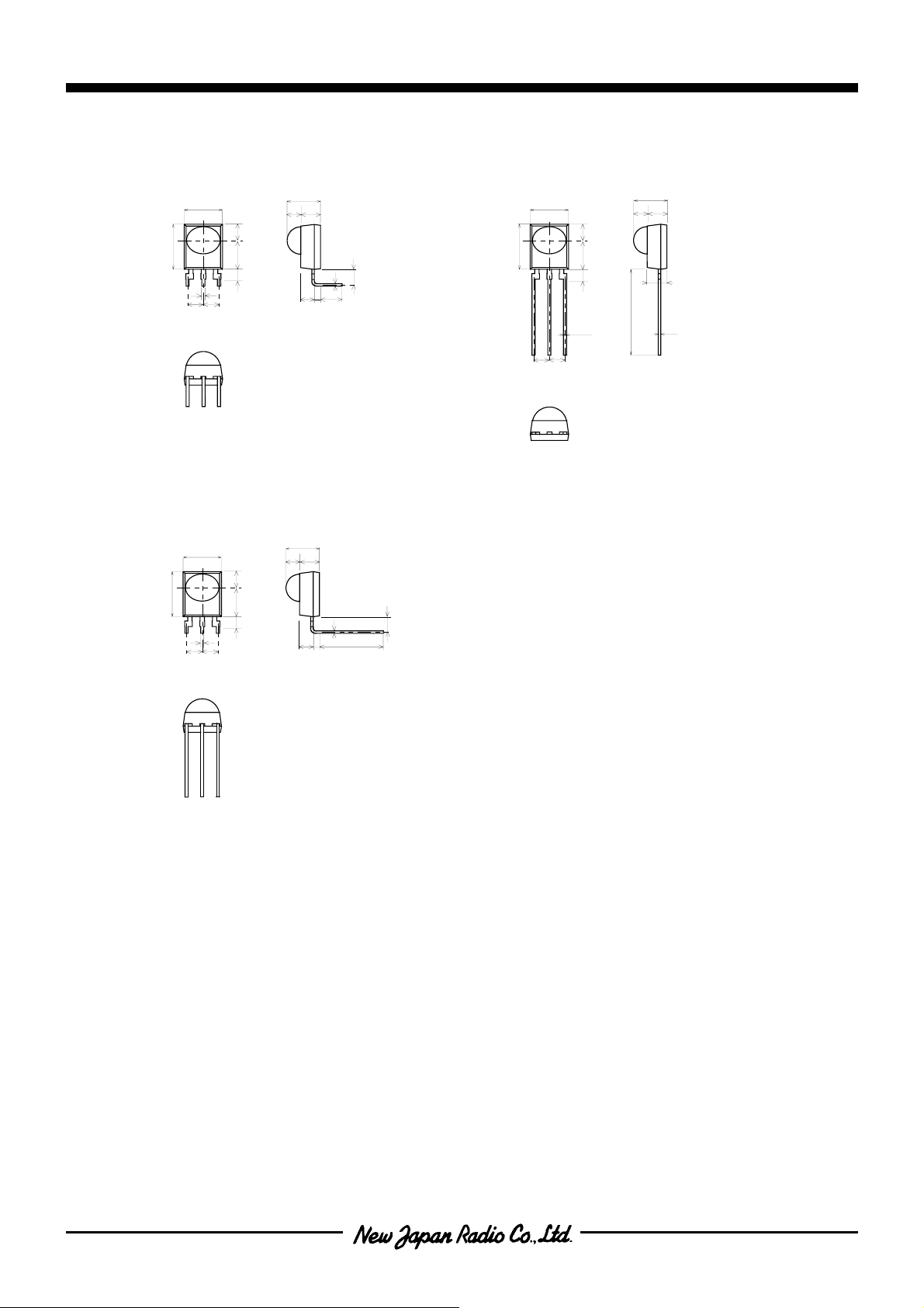
OUTLINE
NJL21H/21V/22H/23H/24H000
6.2
0.5
2.54 2.54
123
2.6
4.7
1.6
7.3
NJL21H000A
UNIT:mm
6.2
2.54
0.5
2.54
2.6
4.7
1.6
7.3
5.4
2.2
3.2
2.2
1:OUT
2:GND
3:Vcc
5.4
2.2
3.2
2.2
6.2
7.3
0.4
2.5
4.0
1.0
2.54
123
2.6
4.7
1.6
0.5
2.54
5.4
2.2
2.2
16.5±0 .5
1:OUT
2:GND
3:Vcc
3.2
1.0
0.4
NJL21V000A
UNIT:mm
0.4
1.0
2.5
13.1
1:OUT
2:GND
3:Vcc
123
NJL21H000AF3
UNIT:mm

A
NJL21H/21V/22H/23H/24H000
(5.7)
2.
R
: OUT
: GND
: Vcc
3.51.9
2
0.4
2.5
1.0
6.8
7.6
(7.8)
0.5
2.54
12
2.9
4.7
1.6
16.5 0.5
2.54
3
.
R2
1
2
8
3
(3.8)
(3.2)
NJL21V000A-M
UNIT:mm
(5.7)
6.8
2.54
R
2.9
4.7
1
: OUT
2
: GND
3
: Vcc
8
.
2
7.6
(7.8)
0.5
2.54
(3.8)
3.51.9
2
.
2
R
(10.8)
4.0
0.9
10.8
12
3
2.54
3- 0.8
2.54
PCB pattern
NJL21H000A-M
UNIT:mm
A
t
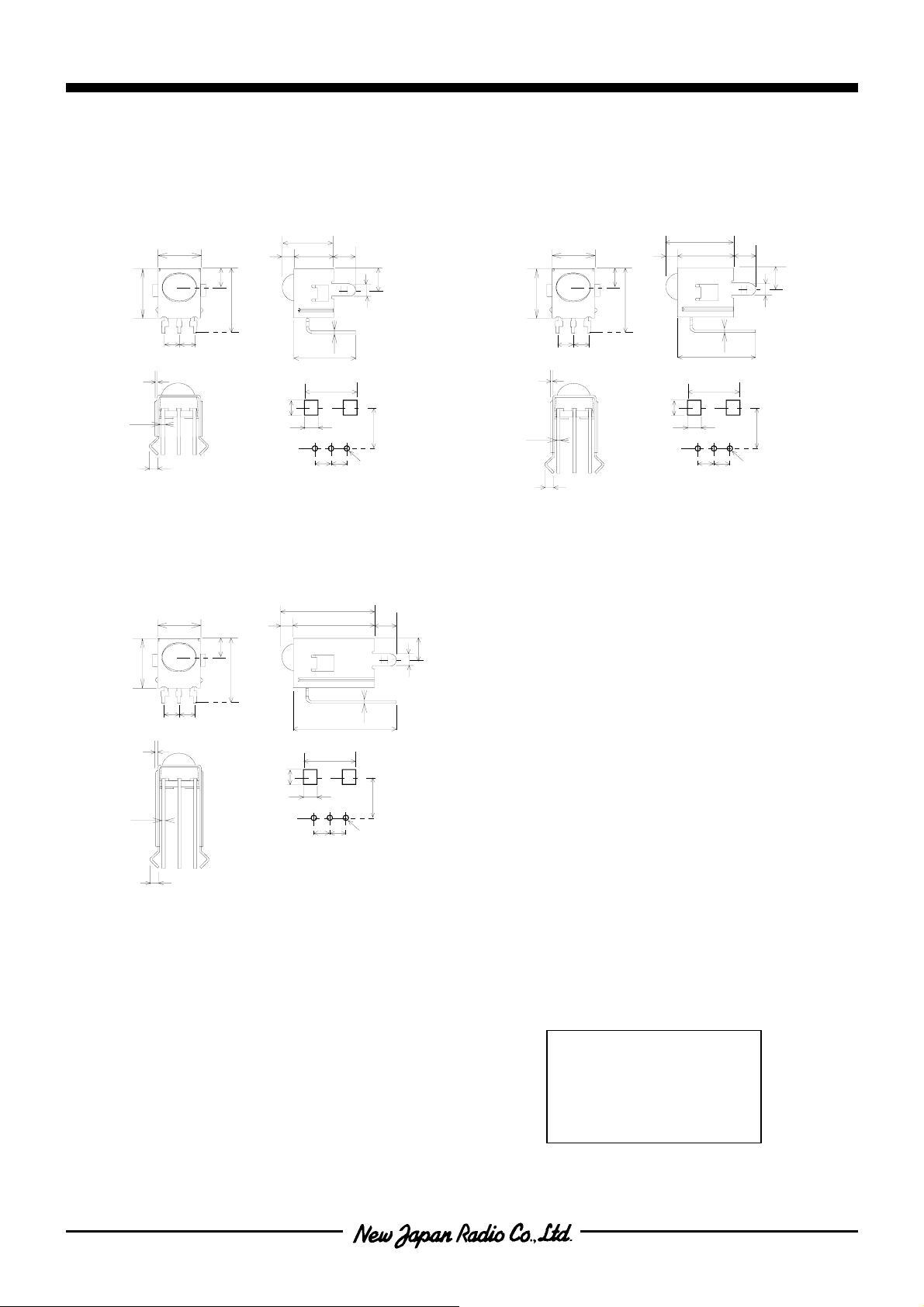
NJL21H/21V/22H/23H/24H000
7.0
8.0
2.54
2.54
0.3
0.5
123
1.3
NJL22H000A
UNIT:mm
7.0
8.0
3.0
10.2
1:OUT
2:GND
3:Vcc
3.0
10.2
1.9
1.9
8.0
6.1
(9.6)
2.5
2.0
2.54
PCB Pattern
15.0
8.2
13.1
11.0
1.9
9.1
(12.6)
2.5
2.0
2.54
PCB Pattern
0.5
1.3
8.0
0.3
7.0
2.54
123
2.54
3.0
10.2
1:OUT
2:GND
3:Vcc
3.5
3.5
2.0
0.4
6.7
3-φ0.8
2.54
3.5
3.5
2.0
0.4
8.2
6.7
3-φ0.8
2.54
NJL23H000A
UNIT:mm
3.5
3.5
2.0
1.3
0.3
0.5
2.54
2.54
123
1:OUT
2:GND
3:Vcc
(16.6)
8.2
2.5
2.0
2.54
PCB Pattern
NJL24H000A
UNIT:mm
2.54
0.4
6.7
3-φ0.8
1. Tolerance is ±0.3mm unless otherwise noted.
2. Ground metal case on PCB. Metal case is no
connected to GND pin inside.Tolerance is ±0.3mm
unless otherwise noted.
[CAUTION]
The specifications on this databook are only
given for information , without any guarantee
as regards either mistakes or omissions. The
application circuits in this databook are
described only to show representative usages
of the product and not intended for the
guarantee or permission of any right including
the industrial rights.
 Loading...