

Page 1

MB879
Intel Pentium® M
ATI Radeon Xpress 200
Mini-ITX Motherboard
USER’S MANUAL
Version 1.0
Page 2

Acknowledgments
Award is a registered trademark of Award Software
International, Inc.
PS/2 is a trademark of International Business Machines
Corporation.
Intel and Pentium M are registered trademarks of Intel
Corporation.
Microsoft Windows is a registered trademark of Microsoft
Corporation.
All other product names or trademarks are properties of their
respective owners.
ii MB879 User’s Manual
Page 3

Table of Contents
Introduction............................................................... 1
Product Description..............................................................1
Checklist...............................................................................2
MB879 Specifications..........................................................3
Board Dimensions................................................................ 4
Installations............................................................... 5
Installing the CPU................................................................ 6
Installing the Memory...........................................................7
Setting the Jumpers.............................................................. 8
Jumper Locations on MB879................................................9
JP1: COM4 RS232 +5V / +12V Power Setting................. 10
JP2: LVDS Panel Voltage Selection.................................. 10
JP3: COM3 RS232 +5V / +12V Power Setting................. 10
JP4: CPU FSB Selection.....................................................10
JP5: Clear CMOS Setting...................................................11
[........................................................................................... 11
SW1: LVDS Resolution Switch Setting.............................11
Connectors on MB879....................................................... 12
Connector Locations on MB879.........................................13
CN1: PS/2 Keyboard and PS/2 Mouse Connectors............14
CN2: S-Video and RCA Connector for TV out................. 14
CN3: COM1 and VGA Connector..................................... 14
.............................................................................................15
CN4: 10/100 LAN RJ-45 and USB1/2 Ports......................15
CN5: 1394 Connector.........................................................15
CN6: SPDIF Out Connector...............................................15
CN7: Gigabit LAN RJ-45 and USB3/4 Ports.....................15
CN8: Audio Connector.......................................................15
FAN1: CPU Fan Power Connector.................................... 15
FAN2: System Fan Power Connector.................................15
J1: Floppy Drive Connector................................................16
IDE1: IDE Connector.........................................................16
J2: ATX Power Supply Connector..................................... 17
J3: TV Out Header (RCA & S-Video)............................... 17
J4: COM2, COM3, COM4 Serial Ports............................. 17
J5: IrDA Connector............................................................ 18
MB879 User’s Manual iii
Page 4

J9, J6: LVDS Connectors (1st channel, 2nd channel).......18
J7: Panel Inverter Power Connector...................................18
J8: Digital I/O.....................................................................18
J10: 1394 Connector...........................................................19
J11: Panel Inverter Power Connector.................................19
J12: Mini PCI Connector....................................................19
.............................................................................................19
J13: Speaker Connector......................................................19
J14: Front Audio Connector............................................... 19
REMARKS: To use the front audio connector, the jumpers
on pin 1-3 and pin 2-4 must be removed........................... 19
J15, J16: Serial ATA Connectors....................................... 20
J17: Wake On LAN Connector.......................................... 20
J18: System Function Connector........................................20
J19: USB5 / USB6 Connector............................................ 20
J20: CD-In Pin Header....................................................... 21
J21: Power LED Connector................................................ 21
J22: Compact Flash Connector (solder side, option)......... 21
PCI1: PCI Slot (supports 2 Masters).................................. 21
PCIE1: PCI-E(x1) Slot....................................................... 21
This page is intentionally left blank...................................22
BIOS Setup.............................................................. 23
BIOS Introduction.............................................................. 24
BIOS Setup......................................................................... 24
Standard CMOS Setup....................................................... 26
Advanced BIOS Features....................................................29
Advanced Chipset Features................................................ 32
Power Management Setup..................................................40
PNP/PCI Configurations ................................................... 42
PC Health Status ................................................................43
Frequency/Voltage Control ............................................... 44
Load Fail-Safe Defaults...................................................... 45
Load Optimized Defaults....................................................45
Set Supervisor/User Password............................................ 45
Save & Exit Setup...............................................................45
Exit Without Saving........................................................... 45
Drivers Installation................................................. 47
ATI Radeon Xpress 200 Series Drivers Installation.......... 48
Realtek AC97 Codec Audio Driver Installation.................51
iv MB879 User’s Manual
Page 5

LAN Driver Installation..................................................... 53
Appendix................................................................. 57
A. I/O Port Address Map................................................... 57
B. Interrupt Request Lines (IRQ).......................................58
C. Watchdog Timer Configuration.....................................59
MB879 User’s Manual v
Page 6
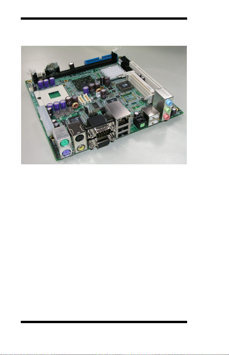
THE MB879 MINI ITX MOTHERBOARD
vi MB879 User’s Manual
Page 7

INTRODUCTION
Introduction
Product Description
Designed for gaming and multimedia applications, the MB879 Mini ITX
board incorporates the ATi Xpress 200 chipset, supporting CPU front side bus
of 400MHz and 533MHz. The board accommodates Pentium® M and
Celeron® M processors with speeds up to 2.26GHz and one DDR2 DIMM
memory.
The MB879 comes with the RC410MD Integrated Graphics Processor (IGP)
that integrates 2D/3D graphics and a system controller in a single chip. The
RC410MD delivers the best performance of all integrated graphics and core
logic products in the market. It incorporates an ATI Radeon X300-based
graphics core, which is coupled with 64-bit DDR/DDR2 SDRAM system
memory interface for optimal performance.
The main features of the board are:
Supports Pentium® M / Celeron® M processors (90nm process, 3xx
only, 4xx not supported)
Supports up to 2.26GHz, 400MHz/533MHz FSB
One DDR2 SDRAM DIMM, Max. 1GB memory, supports DDR2-
400/533/667
Onboard 10/100 BaseT and Gigabit LAN (MB879F)
ATi Mobility Radeon 9600 VGA for CRT / TV out / LVDS
2x SATA, 6x USB 2.0, 4x COM, Watchdog timer, 1394
1x PCI, 1x MiniPCI, 1xPCI-E(x1) slots
Dimensions of the board are 170mm x 170mm.
MB879 User’s Manual 1
Page 8

INTRODUCTION
Checklist
Your MB879 package should include the items listed below.
• The MB879 Pentium
• This User’s Manual
• 1 CD containing chipset drivers and flash memory utility
®
M Mini-ITX motherboard
2 MB879 User’s Manual
Page 9

INTRODUCTION
MB879 Specifications
[
CPU Socket Socket 479 or FBGA on board
CPU Supported Intel Pentium® M / Celeron® M, 90nm process, (3xx only, 4xx not
CPU Voltage 0.700V ~ 1.708V
CPU Speed / FSB Up to 2.26GHz / 533MHz FSB
Green /APM APM1.2
Chipset ATI Radeon Xpress 200 (RC410MD) / SB450 chipset
BIOS Award BIOS, support ACPI function
Cache 512K/1M/2M Level 2 (CPU integrated)
Memory 1x DDR2 400/533/667 socket (single channel, w/o ECC),
VGA ATi RC410MD built Mobility Radeon 9600 (M10) graphic core.
LVDS ATi RC410MD built controller and transmitter, supports 24-bit
LAN
supported)
NB: ATi Radeon Xpress 200 (RC410MD), 707-ball FCBGA
SB: ATi SB450, 564-ball BGA
Max.1GB
Supports DirectX 9.0 and supports CRT, LVDS & TV-out
single/dual channels LVDS
- Realtek RTL8100C-LF (10/100) LAN controller x1
- Marvell 88E8052 PCI Express x1 Gigabit LAN controller
USB ATi SB450 built-in USB2.0 host controller, supports 6 ports
Audio ATi SB450 built-in Audio controller + AC97 Codec ALC655 for
Serial ATA ATi SB450 built-in SATA host controller, supports 2 ports
1394 (option) TI TSB43LV22 (dual port)
Local bus IDE ATi SB450 built-in two channels Ultra DMA 100/133
(option)
5.1 CH (Line-out, Line-in & Microphone)
NS LM4950 (8-ohm 2W stereo audio power amplifier)
- IDE1: 40 pins box-header; IDE2: Compact Flash (option)
LPC I/O ITE IT8712: COM1, COM2 (RS232), IrDA, Floppy, hardware
2nd I/O Fintek F81216D for COM3 / COM4
Edge Connector PS/2 Connector x1 for keyboard/mouse
Onboard Headers /
Connectors
Expansion Slot PCI slot (32bits/33MHz) x1
Digital I/O Supports 4 in, 4 out
Watchdog Timer Yes (256 segments, 0, 1, 2…255. sec/min)
Power Connector Standard ATX 12V
System Voltage +5V, +12V, -12V, 5VSB, -5V & 3.3V
Other Features Modem Wakeup, LAN Wakeup
Board Size 170 x 170mm
monitor (3 thermal inputs, 4 voltage monitor inputs, VID0-5 & 2
Fan Header). Parallel port not use
Gigabit LAN RJ-45 + dual USB stack connector
10/100 LAN RJ45 + dual USB stack connector
DB9 & DB15 stack connector x1 for COM 1 and VGA
RCA Jack x1 +S-Video for TV-Out
SPDIF/OUT connector x1
1394 Connector x1
RCA Jack 3x1 for Audio (Line-Out, Line-In & Mic) – 1U height
DF13-20 x2 for LVDS
40 pins, 2.54mm, box-header x 1 for IDE1
5x2 pins pin-header x1 for 2 USB ports
8 pins pin-header x1 for 1394
30 pins pin-header x1 for COM2/3/4
Slim Floppy connector x 1
5 pins pin-header x 1 for IrDA
PCI-Express (x1) x1 (align w/ PCI slot); Mini PCI connector x1
MB879 User’s Manual 3
Page 10
INTRODUCTION
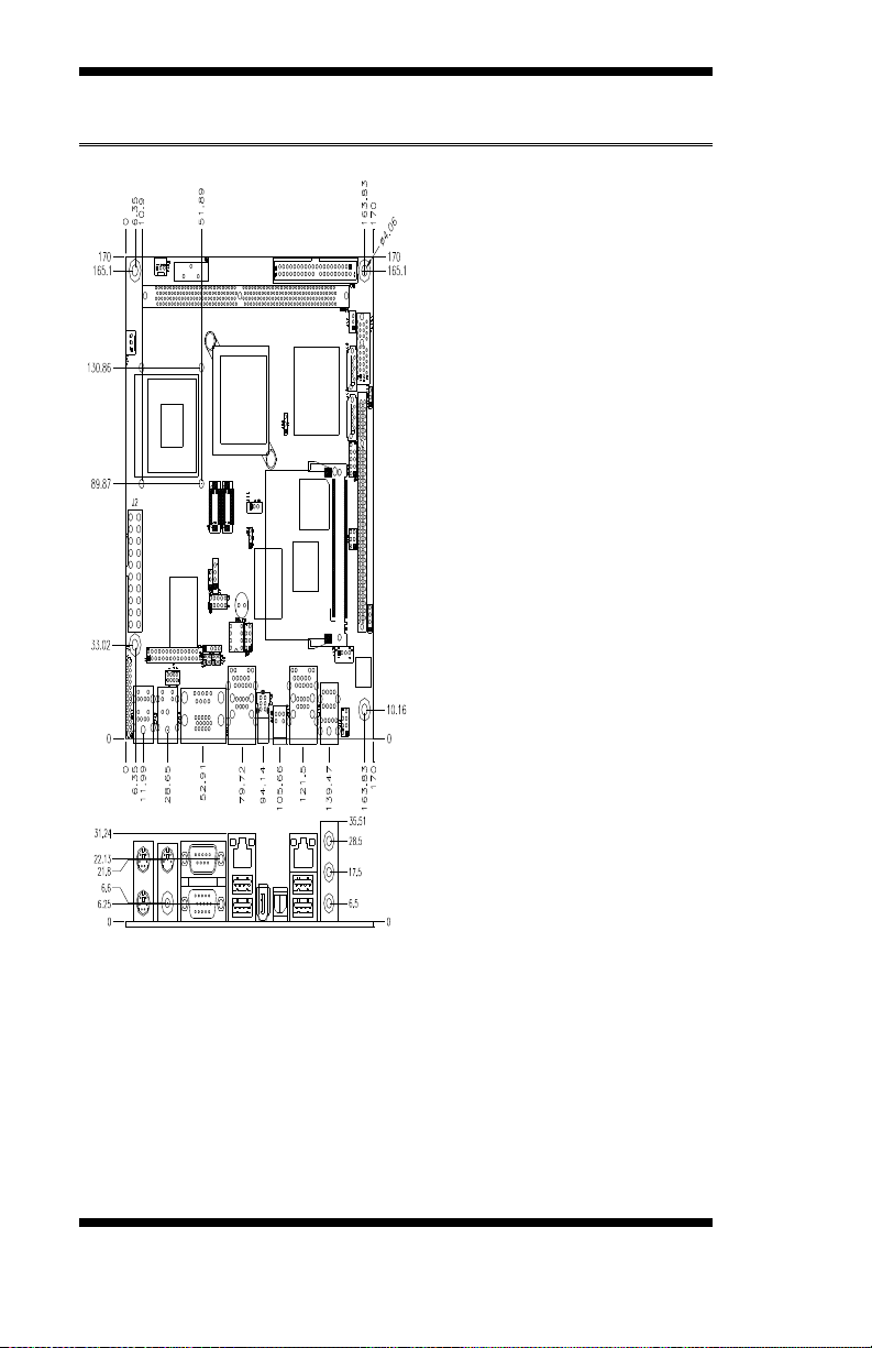
Board Dimensions
4 MB879 User’s Manual
Page 11

INSTALLATIONS
Installations
This section provides information on how to use the jumpers and
connectors on the MB879 in order to set up a workable system. The
topics covered are:
Installing the CPU...........................................................................
Installing the Memory.....................................................................
Setting the Jumpers.........................................................................
Connectors on MB879....................................................................
MB879 User’s Manual 5
Page 12
INSTALLATIONS
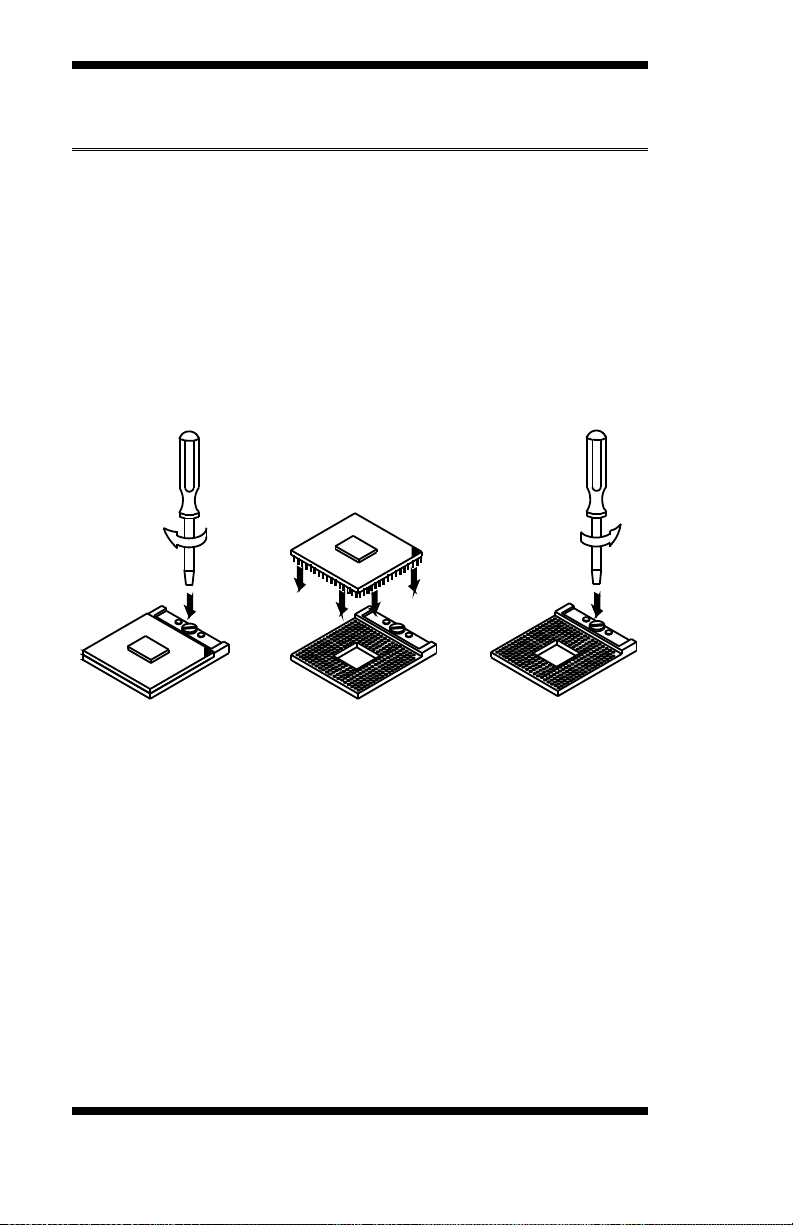
Installing the CPU
The MB879 board supports a Socket 479 processor socket for Intel
Pentium® M or Celeron® M processors.
The processor socket comes with a screw to secure the processor. As
shown in the left picture below, loosen the screw first before inserting
the processor. Place the processor into the socket by making sure the
notch on the corner of the CPU corresponds with the notch on the
inside of the socket. Once the processor has slide into the socket,
fasten the screw. Refer to the figures below.
®
NOTE: Ensure that the CPU heat sink and the CPU top surface are
in total contact to avoid CPU overheating problem that
would cause your system to hang or be unstable.
6 MB879 User’s Manual
Page 13
INSTALLATIONS
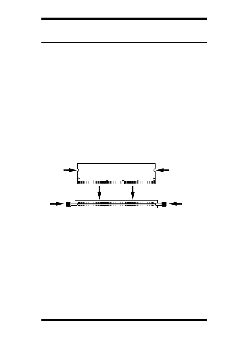
DDR2 Module
Lock Lock
Lock Lock
Installing the Memory
The MB879 board supports one DDR2 memory socket for a maximum
total memory of 1GB in DDR2 memory type.
Installing and Removing Memory Modules
To install the DDR2 modules, locate the memory slot on the board and
perform the following steps:
1. Hold the DDR2 module so that the key of the DDR2 module align
with those on the memory slot.
2. Gently push the DDR2 module in an upright position until the clips
of the slot close to hold the DDR2 module in place when the DDR2
module touches the bottom of the slot.
3. To remove the DDR2 module, press the clips with both hands.
MB879 User’s Manual 7
Page 14

INSTALLATIONS
Setting the Jumpers
Jumpers are used on MB879 to select various settings and features
according to your needs and applications. Contact your supplier if you
have doubts about the best configuration for your needs. The following
lists the connectors on MB879 and their respective functions.
Jumper Locations on MB879.............................................................
JP1: COM4 RS232 +5V / +12V Power Setting................................
JP2: LVDS Panel Voltage Selection.................................................
JP3: COM3 RS232 +5V / +12V Power Setting................................
JP4: CPU FSB Selection....................................................................
JP5: Clear CMOS Setting..................................................................
SW1: LVDS Resolution Switch Setting............................................
8 MB879 User’s Manual
Page 15
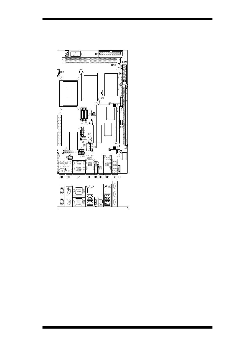
Jumper Locations on MB879
INSTALLATIONS
Jumpers on MB879........................................................................... Page
JP1: COM4 RS232 +5V / +12V Power Setting................................
JP2: LVDS Panel Voltage Selection.................................................
JP3: COM3 RS232 +5V / +12V Power Setting................................
JP4: CPU FSB Selection....................................................................
JP5: Clear CMOS Setting..................................................................
SW1: LVDS Resolution Switch Setting............................................
MB879 User’s Manual 9
Page 16
INSTALLATIONS
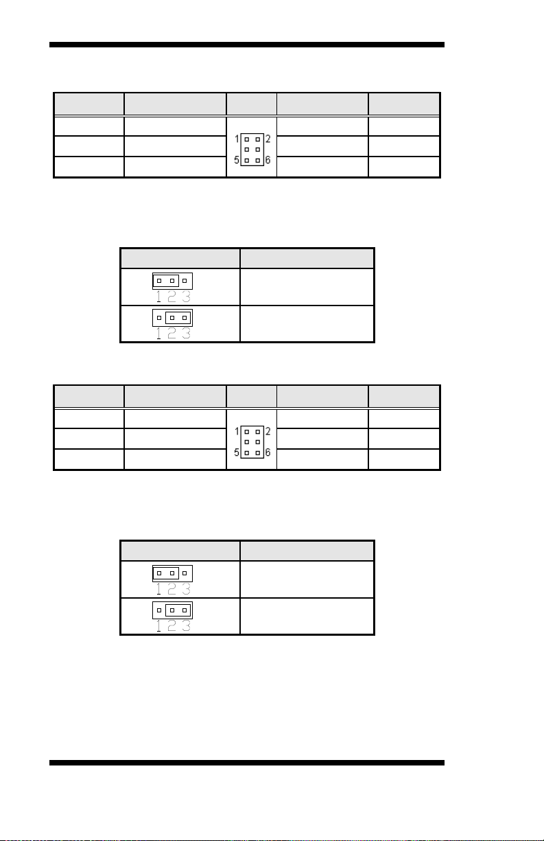
JP1: COM4 RS232 +5V / +12V Power Setting
Pin #
Signal Name JP1 Signal Name
1 RI
3 RI (Default)
5 RI
+12V 2
RI (Default) 4
+5V 6
Pin #
COM4 Settings: Pin 1-2 short = +12V, Pin 5-6 short = +5V, Pin 3-
4 Standard COM Port
JP2: LVDS Panel Voltage Selection
JP2 LVDS Voltage
3.3V
5V
JP3: COM3 RS232 +5V / +12V Power Setting
Pin #
Signal Name JP3 Signal Name
1 RI
3 RI (Default)
5 RI
+12V 2
RI (Default) 4
+5V 6
Pin #
COM3 Settings: Pin 1-2 short = +12V, Pin 5-6 short = +5V, Pin 3-
4 Standard COM Port
JP4: CPU FSB Selection
JP4 CPU FSB
400MHz
533MHz
10 MB879 User’s Manual
Page 17
INSTALLATIONS
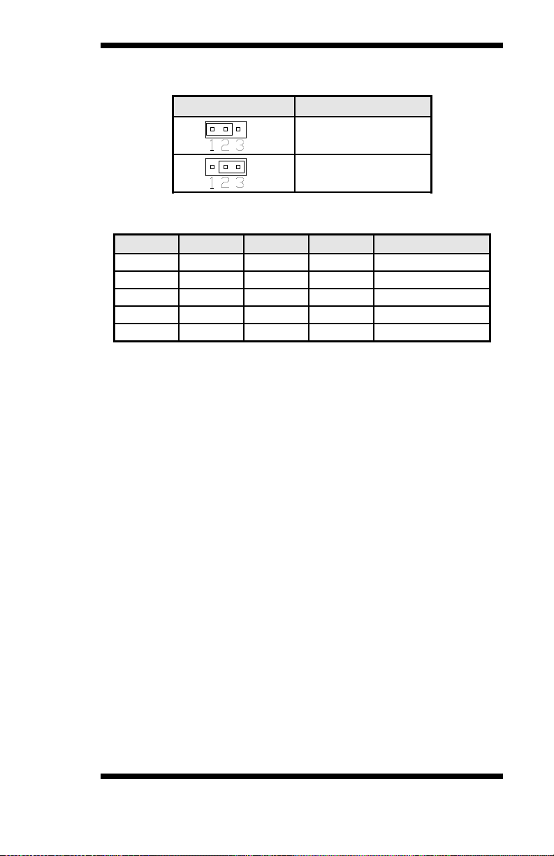
JP5: Clear CMOS Setting
JP5 Setting
Normal
Clear CMOS
[
SW1: LVDS Resolution Switch Setting
SW1-1 SW1-2 SW1-3 SW1-4 Resolution
OFF ON ON OFF 800x600
ON OFF ON OFF 1024x768
OFF OFF ON OFF 1280 X 1024
ON ON OFF OFF 1400 X 1050
OFF OFF OFF OFF CRT Only
MB879 User’s Manual 11
Page 18

INSTALLATIONS
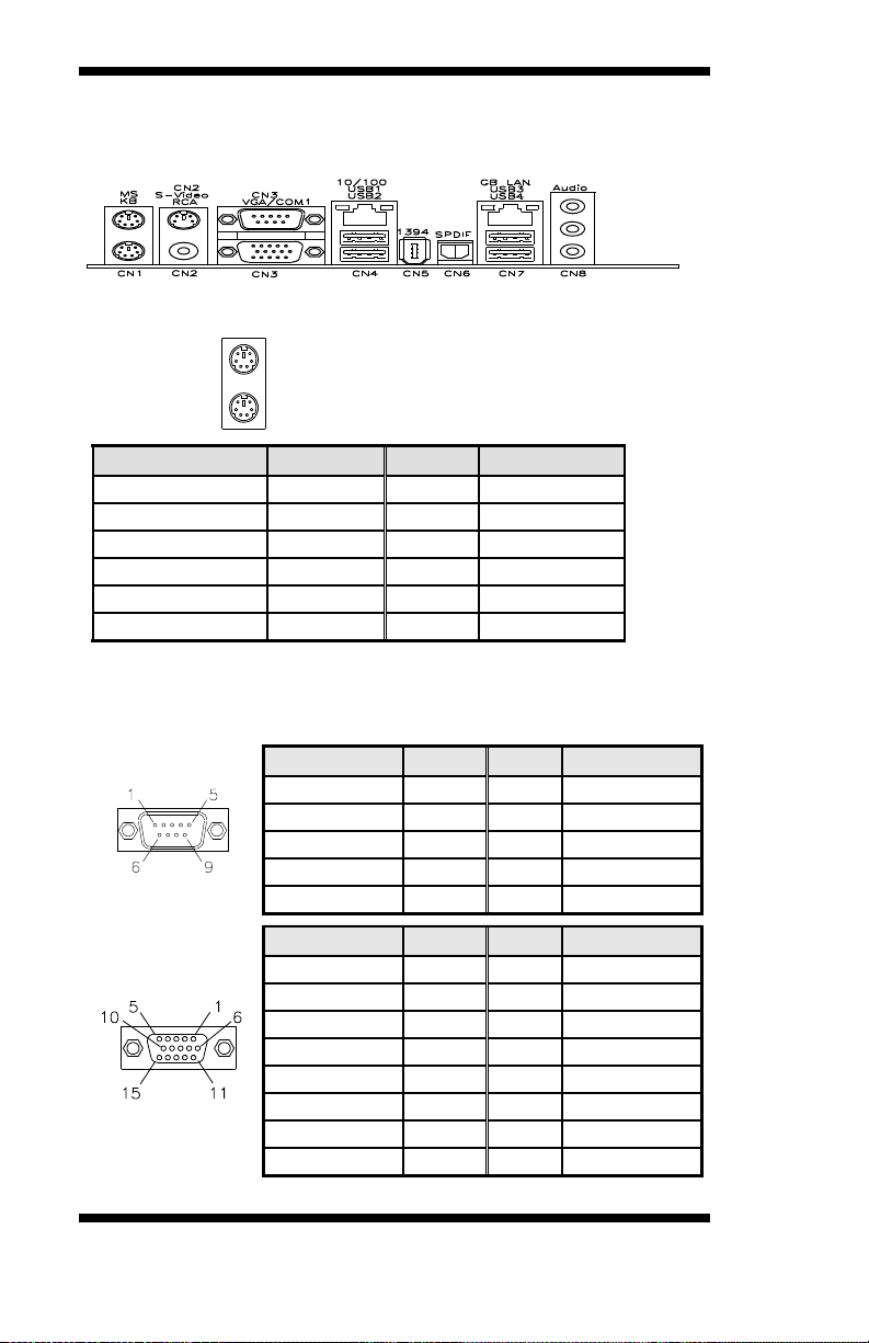
Connectors on MB879
The connectors on MB879 allow you to connect external devices such
as keyboard, floppy disk drives, hard disk drives, etc. The following
table lists the connectors on MB879 and their respective functions.
Connector Locations on MB879........................................................
CN1: PS/2 Keyboard and PS/2 Mouse Connectors...........................
CN2: S-Video and RCA Connector for TV out................................
CN3: COM1 and VGA Connector....................................................
CN4: 10/100 LAN RJ-45 and USB1/2 Ports.....................................
CN5: 1394 Connector........................................................................
CN6: SPDIF Out Connector..............................................................
CN7: Gigabit LAN RJ-45 and USB3/4 Ports....................................
CN8: Audio Connector......................................................................
FAN1: CPU Fan Power Connector....................................................
FAN2: System Fan Power Connector................................................
J1: Floppy Drive Connector...............................................................
IDE1: IDE Connector........................................................................
J2: ATX Power Supply Connector....................................................
J3: TV Out Header (RCA & S-Video)..............................................
J4: COM2, COM3, COM4 Serial Ports............................................
J5: IrDA Connector...........................................................................
J9, J6: LVDS Connectors (1st channel, 2nd channel)......................
J7: Panel Inverter Power Connector..................................................
J8: Digital I/O....................................................................................
J10: 1394 Connector..........................................................................
J11: Panel Inverter Power Connector................................................
J12: Mini PCI Connector...................................................................
J13: Speaker Connector.....................................................................
J14: Front Audio Connector..............................................................
J15, J16: Serial ATA Connectors......................................................
J17: Wake On LAN Connector.........................................................
J18: System Function Connector.......................................................
J19: USB5 / USB6 Connector...........................................................
J20: CD-In Pin Header......................................................................
J21: Power LED Connector...............................................................
J22: Compact Flash Connector (solder side).....................................
PCI1: PCI Slot (supports 2 Masters).................................................
PCIE1: PCI-E(x1) Slot......................................................................
12 MB879 User’s Manual
Page 19
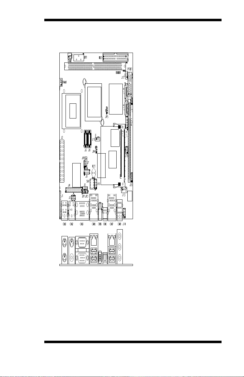
Connector Locations on MB879
INSTALLATIONS
MB879 User’s Manual 13
Page 20
INSTALLATIONS
CN1: PS/2 Keyboard and PS/2 Mouse Connectors
PS/2 Mouse
PS/2 Keyboard
Signal Name Keyboard Mouse Signal Name
Keyboard data 1 1 Mouse data
N.C. 2 2 N.C.
GND 3 3 GND
5V 4 4 5V
Keyboard clock 5 5 Mouse clock
N.C. 6 6 N.C.
CN2: S-Video and RCA Connector for TV out
CN3: COM1 and VGA Connector
[
Signal Name Pin # Pin # Signal Name
DCD 1 6 DSR
RXD 2 7 RTS
TXD 3 8 CTS
DTR 4 9 RI
[[[[
GND 5 10 Not Used
Signal Name Pin # Pin # Signal Name
Red 1 2 Green
Blue 3 4 N.C.
GND 5 6 GND
GND 7 8 GND
N.C. 9 10 GND
+5V 11 12 DDCDAT
HSYNC 13 14 VSYNC
DDCCLK 15
14 MB879 User’s Manual
Page 21
INSTALLATIONS
CN4: 10/100 LAN RJ-45 and USB1/2 Ports
CN5: 1394 Connector
CN6: SPDIF Out Connector
CN7: Gigabit LAN RJ-45 and USB3/4 Ports
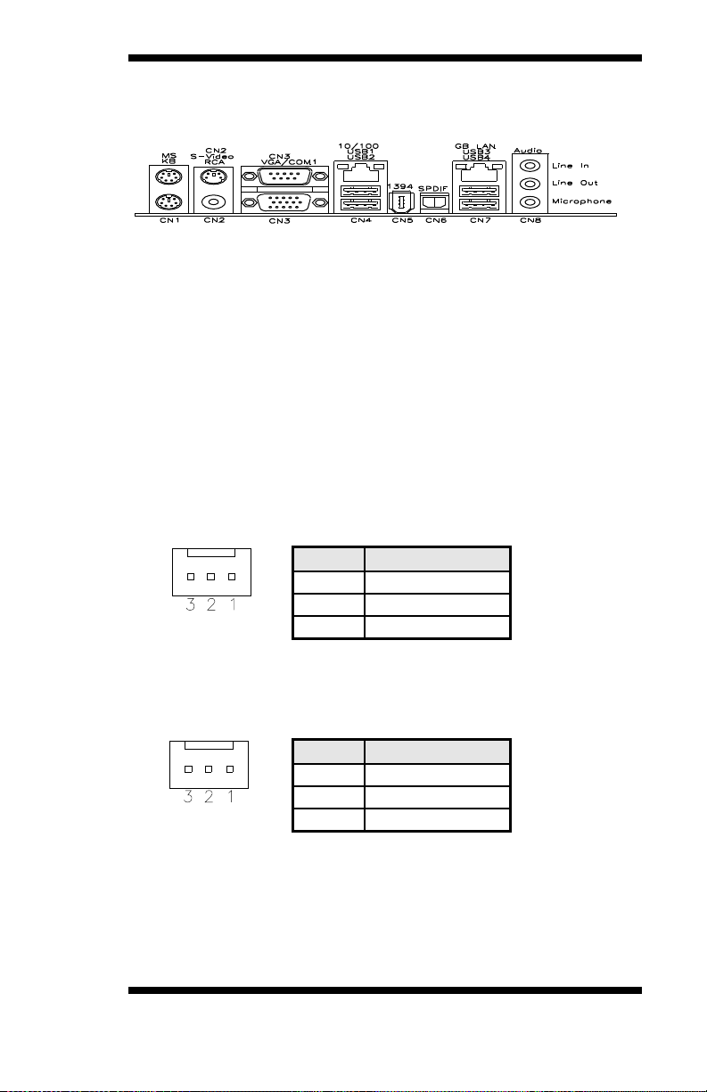
CN8: Audio Connector
The audio connector, from top to bottom, is composed of Line in, Line
out and Microphone jacks.
FAN1: CPU Fan Power Connector
FAN1 is a 3-pin header for the CPU fan with 12V (500mA).
Pin # Signal Name
1 Ground
2 +12V
3 Rotation detection
FAN2: System Fan Power Connector
FAN2 is a 3-pin header for system fans. The fan must be 12V
(500mA).
Pin # Signal Name
1 Ground
2 +12V
3 Rotation detection
MB879 User’s Manual 15
Page 22

INSTALLATIONS
J1: Floppy Drive Connector
J1 is a slim 26-pin connector and will support up to 2.88MB FDD.
Signal Name Pin # Pin # Signal Name
VCC 1 2 INDEX
VCC 3 4 DRV_SEL
VCC 5 6 DSK_CH
NC 7 8 NC
NC 9 10 MOTOR
DINST 11 12 DIR
NC 13 14 STEP
GND 15 16 WDATA
GND 17 18 WGATE
GND 19 20 TRACK
NC 21 22 WPROT
GND 23 24 RDATA
GND 25 26 SIDE
IDE1: IDE Connector
Signal Name Pin # Pin # Signal Name
Reset IDE 1 2 Ground
Host data 7 3 4 Host data 8
Host data 6 5 6 Host data 9
Host data 5 7 8 Host data 10
Host data 4 9 10 Host data 11
Host data 3 11 12 Host data 12
Host data 2 13 14 Host data 13
Host data 1 15 16 Host data 14
Host data 0 17 18 Host data 15
Ground 19 20 Protect pin
DRQ0 21 22 Ground
Host IOW 23 24 Ground
Host IOR 25 26 Ground
IOCHRDY 27 28 Host ALE
DACK0 29 30 Ground
IRQ14 31 32 No connect
Address 1 33 34 No connect
Address 0 35 36 Address 2
Chip select 0 37 38 Chip select 1
Activity 39 40 Ground
16 MB879 User’s Manual
Page 23

J2: ATX Power Supply Connector
11 1
Signal Name Pin # Pin # Signal Name
3.3V 11 1 3.3V
-12V 12 2 3.3V
Ground 13 3 Ground
PS-ON 14 4 +5V
Ground 15 5 Ground
Ground 16 6 +5V
Ground 17 7 Ground
-5V 18 8 Power good
+5V 19 9 5VSB
20 10
+5V 20 10 +12V
J3: TV Out Header (RCA & S-Video)
Signal Name Pin Pin Signal Name
NC 1 2 NC
Y 3 4 Ground
C 5 6 Ground
COMP 7 8 Ground
INSTALLATIONS
J4: COM2, COM3, COM4 Serial Ports
Pin # Signal Name (RS-232)
1 DCD, Data carrier detect
2 RXD, Receive data
3 TXD, Transmit data
4 DTR, Data terminal ready
5 Ground
6 DSR, Data set ready
7 RTS, Request to send
8 CTS, Clear to send
9 RI, Ring indicator
10 No Connect.
MB879 User’s Manual 17
Page 24

INSTALLATIONS
J5: IrDA Connector
Pin # Signal Name
1 +5V
2 No connect
3 Ir RX
4 Ground
5 Ir TX
J9, J6: LVDS Connectors (1st channel, 2nd channel)
The LVDS connectors are composed of the first channel (J9) and
second channel (J6) to support 18/36-bit or 24/48-bit.
Signal Name Pin # Pin #
TX0- 2 1 TX0+
Ground 4 3 Ground
TX1- 6 5 TX1+
5V/3.3V 8 7 Ground
TX3- 10 9 TX3+
TX2- 12 11 TX2+
Ground 14 13 Ground
TXC- 16 15 TXC+
5V/3.3V 18 17 ENABKL
+12V 20 19 +12V
J7: Panel Inverter Power Connector
Pin # Signal Name
1 +12V (1A)
2 Ground
3 LCDVDD
4 ENABKL
J8: Digital I/O
Signal Name Pin Pin Signal Name
GND 1 2 VCC
OUT3 3 4 OUT1
OUT2 5 6 OUT0
IN3 7 8 IN1
IN2 9 10 IN0
Signal Name
18 MB879 User’s Manual
Page 25

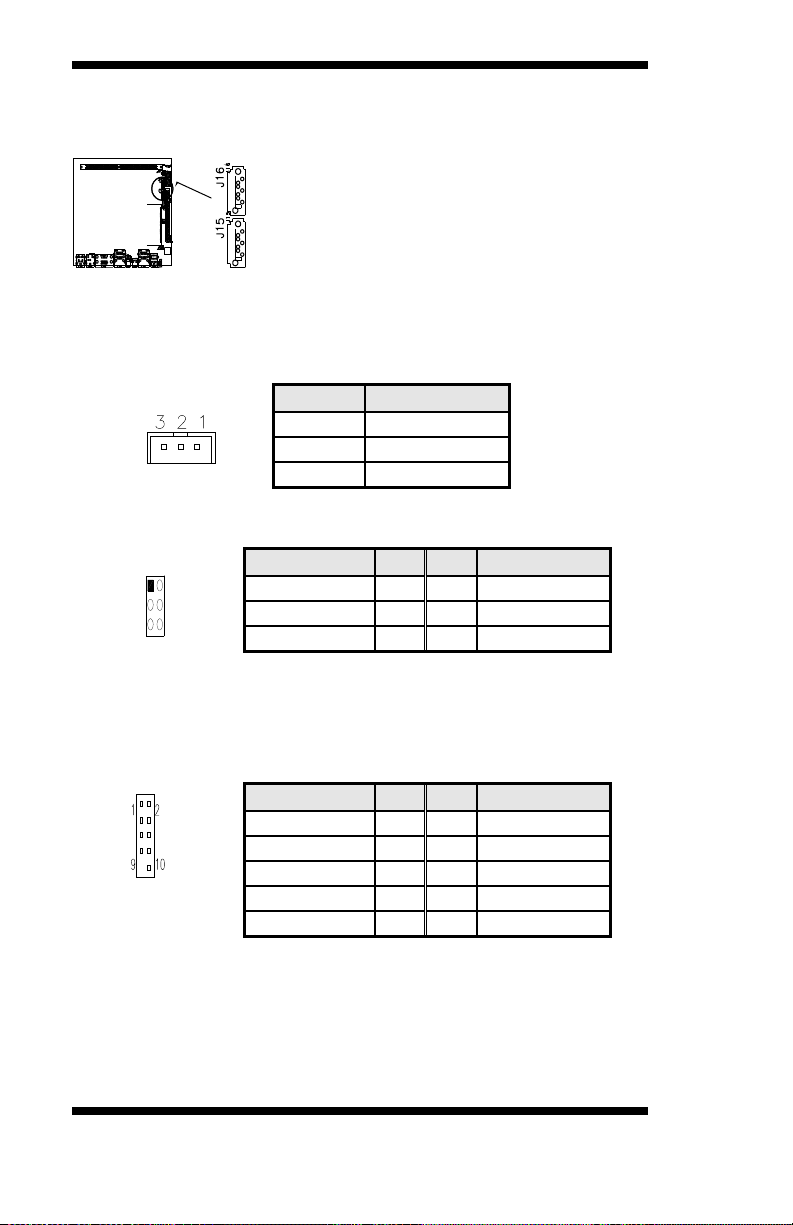
J10: 1394 Connector
Signal Name Pin Pin Signal Name
TPA+ 1 2 TPB+
TPA- 3 4 TPB+12V 5 6 NC
GND 7 8 NC
J11: Panel Inverter Power Connector
Pin # Signal Name
1 +12V (1A)
2 NC
3 Ground
J12: Mini PCI Connector
INSTALLATIONS
J13: Speaker Connector
The J15 connector supports 2W/8ohm stereo audio power amplifier.
Pin # Signal Name
1 Audio L
2 Ground
3 Ground
4 Audio R
J14: Front Audio Connector
Signal Name Pin Pin Signal Name
Rear Audio R 1 5 Rear Audio L
Front Audio R 2 6 Front Audio L
Mic In 3 7 VREF Out
Ground 4 8
REMARKS: To use the front audio connector, the jumpers on pin 13 and pin 2-4 must be removed.
MB879 User’s Manual 19
Page 26
INSTALLATIONS
J15, J16: Serial ATA Connectors
J17: Wake On LAN Connector
J17 is a 3-pin header for the Wake On LAN function. Wake On LAN
will function properly only with an ATX power supply with 5VSB that
has 200mA.
Pin # Signal Name
1 +5VSB
2 Ground
3 -PME
J18: System Function Connector
Signal Name Pin Pin Signal Name
Ground 1 2 PS_ON
5V 3 4 HDD Active
Ground 5 7 Reset
ATX power on switch: Pins 1-2
HDD LED: Pins 3-4
Reset switch: Pins 5-6
J19: USB5 / USB6 Connector
Signal Name Pin Pin Signal Name
Vcc 1 2 Vcc
D- 3 4 D-
D+ 5 6 D+
Ground 7 8 Ground
Protect Pin 9 10 NC
20 MB879 User’s Manual
Page 27
INSTALLATIONS
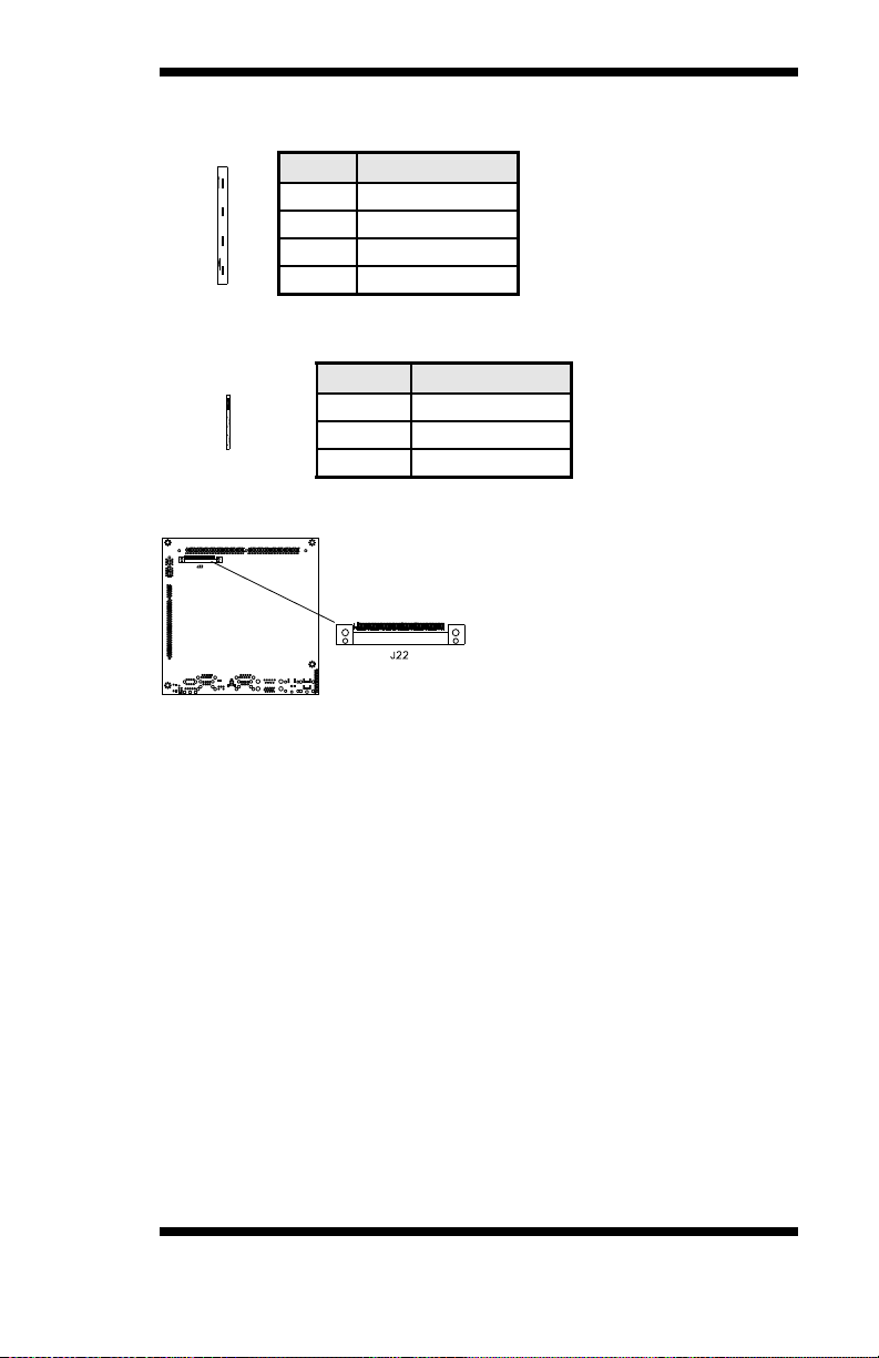
J20: CD-In Pin Header
Pin # Signal Name
1 CD Audio L
2 Ground
3 Ground
4 CD Audio R
J21: Power LED Connector
Pin # Signal Name
1 Vcc
2 NC
3 PLED
J22: Compact Flash Connector (solder side, option)
PCI1: PCI Slot (supports 2 Masters)
PCIE1: PCI-E(x1) Slot
MB879 User’s Manual 21
Page 28

INSTALLATIONS
This page is intentionally left blank.
22 MB879 User’s Manual
Page 29

BIOS SETUP
BIOS Setup
This chapter describes the different settings available in the Award
BIOS that comes with the board. The topics covered in this chapter are
as follows:
BIOS Introduction.............................................................................
BIOS Setup........................................................................................
Standard CMOS Setup......................................................................
Advanced BIOS Features...................................................................
Advanced Chipset Features...............................................................
Integrated Peripherals........................................................................
Power Management Setup.................................................................
PNP/PCI Configurations....................................................................
PC Health Status................................................................................
Frequency/Voltage Control................................................................
Load Fail-Safe Defaults.....................................................................
Load Optimized Defaults...................................................................
Set Supervisor/User Password...........................................................
Save & Exit Setup..............................................................................
Exit Without Saving..........................................................................
MB879 User’s Manual 23
Page 30

BIOS SETUP
BIOS Introduction
The Award BIOS (Basic Input/Output System) installed in your
computer system’s ROM supports Intel processors. The BIOS provides
critical low-level support for a standard device such as disk drives,
serial ports and parallel ports. It also adds virus and password
protection as well as special support for detailed fine-tuning of the
chipset controlling the entire system.
BIOS Setup
The Award BIOS provides a Setup utility program for specifying the
system configurations and settings. The BIOS ROM of the system
stores the Setup utility. When you turn on the computer, the Award
BIOS is immediately activated. Pressing the <Del> key immediately
allows you to enter the Setup utility. If you are a little bit late pressing
the <Del> key, POST (Power On Self Test) will continue with its test
routines, thus preventing you from invoking the Setup. If you still wish
to enter Setup, restart the system by pressing the ”Reset” button or
simultaneously pressing the <Ctrl>, <Alt> and <Delete> keys. You
can also restart by turning the system Off and back On again. The
following message will appear on the screen:
Press <DEL> to Enter Setup
In general, you press the arrow keys to highlight items, <Enter> to
select, the <PgUp> and <PgDn> keys to change entries, <F1> for help
and <Esc> to quit.
When you enter the Setup utility, the Main Menu screen will appear
on the screen. The Main Menu allows you to select from various setup
functions and exit choices.
24 MB879 User’s Manual
Page 31

BIOS SETUP
Phoenix - AwardBIOS CMOS Setup Utility
Standard CMOS Features Frequency/Voltage Control
Advanced BIOS Features Load Fail-Safe Defaults
Advanced Chipset Features Load Optimized Defaults
Integrated Peripherals Set Supervisor Password
Power Management Setup Set User Password
PnP/PCI Configurations Save & Exit Setup
PC Health Status Exit Without Saving
ESC : Quit : Select Item
F10 : Save & Exit Setup
Time, Date, Hard Disk Type…
The section below the setup items of the Main Menu displays the
control keys for this menu. At the bottom of the Main Menu just below
the control keys section, there is another section, which displays
information on the currently highlighted item in the list.
Note: If the system cannot boot after making and saving system
changes with Setup, the Award BIOS supports an override
to the CMOS settings that resets your system to its default.
Warning: It is strongly recommended that you avoid making any
changes to the chipset defaults. These defaults have been
carefully chosen by both Award and your system
manufacturer to provide the absolute maximum
performance and reliability. Changing the defaults could
cause the system to become unstable and crash in some
cases.
MB879 User’s Manual 25
Page 32

BIOS SETUP
Standard CMOS Setup
“Standard CMOS Setup” choice allows you to record some basic
hardware configurations in your computer system and set the system
clock and error handling. If the board is already installed in a working
system, you will not need to select this option. You will need to run
the Standard CMOS option, however, if you change your system
hardware configurations, the onboard battery fails, or the
configuration stored in the CMOS memory was lost or damaged.
Phoenix – Award Work stationBIOS CMOS Setup Utility
Date (mm:dd:yy) Wed, Jul 26 2006 Item Help
Time (hh:mm:ss) 11 : 55 : 00 Menu Level >
Standard CMOS Features
IDE Channel 0 Master None
IDE Channel 0 Slave None
IDE Channel 1 Master None
IDE Channel 1 Slave
IDE Channel 2 Master
IDE Channel 3 Master
Drive A None
Video EGA/VGA
Halt On All , But Keyboard
Base Memory 640K
Extended Memory 980992K
Total Memory 982016K
None
None
None
Change the day, month,
Year and century
At the bottom of the menu are the control keys for use on this menu. If
you need any help in each item field, you can press the <F1> key. It
will display the relevant information to help you. The memory display
at the lower right-hand side of the menu is read-only. It will adjust
automatically according to the memory changed. The following
describes each item of this menu.
Date
The date format is:
Day : Sun to Sat
Month : 1 to 12
Date : 1 to 31
Year : 1999 to 2099
26 MB879 User’s Manual
Page 33

BIOS SETUP
To set the date, highlight the “Date” field and use the PageUp/
PageDown or +/- keys to set the current time.
Time
The time format is: Hour : 00 to 23
Minute : 00 to 59
Second : 00 to 59
To set the time, highlight the “Time” field and use the <PgUp>/
<PgDn> or +/- keys to set the current time.
IDE Channel Master/Slave
The onboard PCI IDE connector provides Primary and Secondary
channels for connecting up to two IDE hard disks or other IDE
devices.
Press <Enter> to configure the hard disk. The selections include Auto,
Manual, and None. Select ‘Manual’ to define the drive information
manually. You will be asked to enter the following items.
Capacity : Capacity/size of the hard disk drive
Cylinder : Number of cylinders
Head : Number of read/write heads
Precomp : Write precompensation
Landing Zone : Landing zone
Sector : Number of sectors
The Access Mode selections are as follows:
CHS (HD < 528MB)
LBA (HD > 528MB and supports Logical Block Addressing)
Large (for MS-DOS only)
Auto
Drive A
These fields identify the types of floppy disk drive A or drive B that
has been installed in the computer. The available specifications are:
360KB
5.25 in.
1.2MB
5.25 in.
720KB
3.5 in.
1.44MB
3.5 in.
2.88MB
3.5 in.
MB879 User’s Manual 27
Page 34

BIOS SETUP
Video
This field selects the type of video display card installed in your
system. You can choose the following video display cards:
EGA/VGA For EGA, VGA, SEGA, SVGA
or PGA monitor adapters. (default)
CGA 40 Power up in 40 column mode.
CGA 80 Power up in 80 column mode.
MONO For Hercules or MDA adapters.
Halt On
This field determines whether or not the system will halt if an error is
detected during power up.
No errors The system boot will not be halted for any
error that may be detected.
All errors Whenever the BIOS detects a non-fatal error,
the system will stop and you will be
prompted.
All, But Keyboard The system boot will not be halted for a
keyboard error; it will stop for all other errors
All, But Diskette The system boot will not be halted for a disk
error; it will stop for all other errors.
All, But Disk/Key The system boot will not be halted for a key-
board or disk error; it will stop for all others.
28 MB879 User’s Manual
Page 35

BIOS SETUP
Advanced BIOS Features
This section allows you to configure and improve your system and
allows you to set up some system features according to your
preference.
Phoenix - Award WorkstationBIOS CMOS Setup Utility
CPU Feature Press Enter ITEM HELP
Hard Disk Boot Priority Press Enter
Virus Warni ng Disabled
CPU L1 and L2 Cache
Hyper-Threading Technology
Quick Power On Self Test Enabled
First Boot Device Floppy
Second Boot Device Hard Disk
Third Boot Device CDROM
Boot Other Device Enabled
Boot Up Floppy Seek Disabl ed
Boot Up NumLock Status On
Gate A20 Option Fast
Typematic Rate Setting Disabled
Typematic Rate (Chars/Sec) 6
Typematic Delay (Msec) 250
Security Option Setup
APIC Mode Enabled
MPS Version Control for OS 1.4
OS Select For DRAM>64MB Non-OS2
HDD S.M.A.R.T. Capability Disabled
Advanced BIOS Features
Enabled
Enabled
Menu Level >
CPU Feature
Press Enter to configure the settings relevant to CPU Feature.
Hard Disk Boot Priority
With the field, there is the option to choose, aside from the hard disks
connected, “Bootable add-in Cards” which refers to other external
devices.
Virus Warning
If this option is enabled, an alarm message will be displayed when trying to
write on the boot sector or on the partition table on the disk, which is typical
of the virus.
CPU L1 and L2 Cache
Cache memory is additional memory that is faster than conventional DRAM
(system memory). CPUs from 486-type on up contain internal cache memory,
and most, but not all, modern PCs have additional (external) cache memory.
When the CPU requests data, the system transfers the requested data from the
main DRAM into cache memory, for even faster access by the CPU. These
allow you to enable (speed up memory access) or disable the cache function.
MB879 User’s Manual 29
Page 36

BIOS SETUP
Quick Power On Self Test
When enabled, this field speeds up the Power On Self Test (POST)
after the system is turned on. If it is set to Enabled, BIOS will skip
some items.
First/Second/Third Boot Device
These fields determine the drive that the system searches first for an
operating system. The options available include Floppy, LS120, Hard
Disk, CDROM, ZIP100, USB-Floppy, USB-ZIP, USB-CDROM and
Disable.
Boot Other Device
These fields allow the system to search for an OS from other devices
other than the ones selected in the First/Second/Third Boot Device.
Boot Up Floppy Seek
This feature controls whether the BIOS checks for a floppy drive while
booting up. If it cannot detect one (either due to improper
configuration or its absence), it will flash an error message.
Boot Up NumLock Status
This allows you to activate the NumLock function after you power up
the system.
Gate A20 Option
This field allows you to select how Gate A20 is worked. Gate A20 is a
device used to address memory above 1 MB.
Typematic Rate Setting
When disabled, continually holding down a key on your keyboard will
generate only one instance. When enabled, you can set the two
typematic controls listed next. By default, this field is set to Disabled.
Typematic Rate (Chars/Sec)
When the typematic rate is enabled, the system registers repeated
keystrokes speeds. Settings are from 6 to 30 characters per second.
30 MB879 User’s Manual
Page 37

BIOS SETUP
Typematic Delay (Msec)
When the typematic rate is enabled, this item allows you to set the
time interval for displaying the first and second characters. By default,
this item is set to 250msec.
Security Option
This field allows you to limit access to the System and Setup. The
default value is Setup. When you select System, the system prompts for
the User Password every time you boot up. When you select Setup, the
system always boots up and prompts for the Supervisor Password only
when the Setup utility is called up.
APIC Mode
APIC stands for Advanced Programmable Interrupt Controller. The
default setting is Enabled.
MPS Version Control for OS
This option is specifies the MPS (Multiprocessor Specification)
version for your operating system. MPS version 1.4 added extended
configuration tables to improve support for multiple PCI bus
configurations and improve future expandability. The default setting is
1.4.
OS Select for DRAM > 64MB
This option allows the system to access greater than 64MB of DRAM
memory when used with OS/2 that depends on certain BIOS calls to
access memory. The default setting is Non-OS/2.
HDD S.M.A.R.T. Capability
The default setting is Disabled.
MB879 User’s Manual 31
Page 38

BIOS SETUP
Advanced Chipset Features
This Setup menu controls the configuration of the chipset.
Phoenix - Award WorkstationBIOS CMOS Setup Utility
Current MRC Version 7.4 ITEM HELP
Current FSB Frequency 100 MHz
Current DRAM Frequency 333 MHz
Memory Frequency For Auto
UMA Frame Buffer Size 64MB
Adjust DRAM Timing Press Enter
Adjust PCIE Confg.
Video Display Devices
Tv Standard
Memory Hole
System BIOS Cacheable
Advanced Chipset Features
Press Enter
CRT Force, Other Auto
NTSC
Disabled
Disabled
Menu Level >
Phoenix - Award WorkstationBIOS CMOS Setup Utility
Simple Addr Translation Enable ITEM HELP
LAQ Bypass Enable
PIF Stage Disable
BIU Power Mgmt Disable
Memory Bank Align ment Auto
Channel Map NB 2
Channel Map GFX
Bank0 Map
Bank1 Map
Bank0 Map NB
Bank1 Map NB
Dynamic Clock
AUTO Calibration
AUTO DQS
Address Step Enable
Impedance Control
Phoenix - Award WorkstationBIOS CMOS Setup Utility
Add 10% Extra Current Disabled ITEM HELP
PCIE GFX Overclocking Disabled
Power down unused GFX port Enabled
Power down unused GPP lane
PCIE CARD WORKAROUND
GFX Link Width
SDVO
PCIE GFX SB Payload Size
PCIE GPP SB Payload Size
A-Link & GPP Configuration
Clock Gating for TxClk Disabled
PCIE Hide Unused Port Auto
L0s/L1 ASPM on Al ink-Expre Disabled
ATi GFX Card ASPM L1 Disabled
Adjust DRAM Timing
4
7
13
7
13
Enable
Enable
Disable
Auto
Enable
Adjust PCIE Confg.
Enabled
Enabled
X16
Disabled
64 Bytes
64 Bytes
4-1-1-1-1 Mode
Menu Level >
Menu Level >
Current MRC Version
32 MB879 User’s Manual
Page 39

BIOS SETUP
The default setting is 7.4.
Current FSB Frequency
The default setting is 133 MHz
Current DRAM Frequency
The default setting is 266 MHz.
Memory Frequencty For
The default setting is AUTO.
UMA Frame Buffer Size
Frame Buffer is the video memory that stores data for video display
(frame). This field is used to determine the memory size for Frame
Buffer. Larger frame buffer size increases video performance. The
default setting is 64MB.
Video Display Devices
The default setting is CRT Force, Other Auto.
Tv Standard
The default setting is NTSC.
Memory Hole
In order to improve performance, certain space in memory can be
reserved for ISA cards. This memory must be mapped into the
memory space below 16 MB. The choices are Enabled and Disabled.
System BIOS Cacheable
The setting of Enabled allows caching of the system BIOS ROM at
F000h-FFFFFh, resulting in better system performance. However, if
any program writes to this memory area, a system error may result.
Simple Addr Translation
The default setting is Enable.
LAQ Bypass
The default setting is Enable.
MB879 User’s Manual 33
Page 40

BIOS SETUP
PIF Stage
The default setting is Disable.
BIU Power Mgmt
The default setting is Disable.
Memory Bank Alignment
The default setting is Auto.
Dynamic Clock
The default setting is Enable.
Auto Calibration
The default setting is Enable.
Auto DQS
The default setting is Disable.
Address Step Enable
The default setting is Auto.
Impedance Control
The default setting is Enable.
Add 10% Extra Current
The default setting is Disabled.
PCIE GFX Overclocking
The default setting is Disabled.
Power down unused GFX ports
The default setting is Enabled.
Power down unused GPP lanes
The default setting is Enabled.
PCIE CARD WORKROUND
The default setting is Enabled.
GFX Link Width
The default setting is x16.
34 MB879 User’s Manual
Page 41

SDVO
The default setting is Disabled.
PCIE GFX SB Payload Size
The default setting is 64 Bytes.
PCIE GPP SB Payload Size
The default setting is 64 Bytes.
A-Link & GPP Configuration
This setting controls the A-Link & GPP configuration.
Clock Gating for TxClk
The default setting is Disabled.
PCIE Hide Unused Port
The default setting is Auto.
L0s/L1 ASPM on Alink-Express
The default setting is Disabled.
ATI GFX Card ASPM L1
The default setting is Disabled.
BIOS SETUP
MB879 User’s Manual 35
Page 42

BIOS SETUP
Integrated Peripherals
This section sets configurations for your hard disk and other integrated
peripherals. The first screen shows three main items for user to select.
Once an item selected, a submenu appears. Details follow.
Phoenix - Award WorkstationBIOS CMOS Setup Utility
South OnChip IDE Device
South OnChip PCI Device
Init Display First
Surroundview
USB EHCI Controller
OnChip USB Controller
OnChip USB KBC Controller
USB Mouse Support
IDE HDD Block Mode
Power ON Function
KB Power ON Passwo rd
Hot Key Power ON
Onboard FDC Controller Enabled
Onboard Serial Port 1
Onboard Serial Port 2
UART Mode Select Normal
UR2 Duplex Mode
Watch Dog Timer Select
**** 2nd Super IO Device ****
Onboard Serial Port 3
Serial Port 3 Use IRQ
Onboard Serial Port 4
Serial Port 4 Use IRQ
Phoenix - Award WorkstationBIOS CMOS Setup Utility
IDE DMA transfer access
OnChip IDE Channel0
OnChip IDE Channel1
IDE Prefetch Mode
Primary Master PIO
Primary Slave PIO
Secondary Master PIO
Secondary Slave PIO
Primary Master UDMA
Primary Slave UDMA
Secondary Master UDMA
Secondary Slave UDMA
Integrated Peripherals
Press Enter ITEM HELP
Press Enter
PCI Slot
Disabled
Enabled
Enabled
Enabled
Disabled
Enabled
BUTTON ONLY
Enter
Ctrl-F1
3F8/IRQ4
2F8/IRQ3
Half
Disabled
3E8h
IRQ11
2E8h
IRQ10
South OnChip IDE Device
Enabled ITEM HELP
Enabled
Enabled
Disabled
Auto
Auto
Auto
Auto
Auto
Auto
Auto
Auto
Menu Level >
Menu Level >
36 MB879 User’s Manual
Page 43

BIOS SETUP
Phoenix - Award WorkstationBIOS CMOS Setup Utility
Onboard AC97 Audio
Onboard LAN
Onboard 1394 En abled
South OnChip PCI Device
Auto ITEM HELP
Enabled
Menu Level >
Init Display First
The default setting is PCI Card.
USB EHCI Controller
The options for this field are Enabled and Disabled. By default, this
field is set to Enabled.
OnChip USB Controller
The options for this field are Enabled and Disabled. By default, this
field is set to Enabled.
OnChip USB KBC Controller
The options for this field are Enabled and Disabled. By default, this
field is set to Enabled.
USB Mouse Support
The options for this field are Enabled and Disabled. By default, this
field is set to Disabled.
IDE HDD Block Mode
This field allows your hard disk controller to use the fast block mode
to transfer data to and from your hard disk drive.
Power ON Function
This field is related to how the system is powered on – such as with
the use of conventional power button, keyboard or hot keys. The
default is BUTTON ONLY.
KB Power ON Password
This field allows users to set the password when keyboard power on is
the mode of the Power ON function.
Hot Key Power ON
This field sets certain keys, also known as hot keys, on the keyboard
that can be used as a ‘switch’ to power on the system.
MB879 User’s Manual 37
Page 44

BIOS SETUP
Onboard FDC Controller
Select Enabled if your system has a floppy disk controller (FDC)
installed on the board and you wish to use it. If you install an add-in
FDC or the system has no floppy drive, select Disabled in this field.
Onboard Serial Port
These fields allow you to select the onboard serial and parallel ports
and their address. The default values for these ports are:
Serial Port 1 3F8/IRQ4
Serial Port 2 2F8/IRQ3
Serial Port 3 3E8h/IRQ11
Serial Port 4 2E8h/IRQ10
UART Mode Select
This field determines the UART 2 mode in your computer. The default
value is Normal. Other options include IrDA and ASKIR.
Watch Dog Timer Select
The options available include 2 Min,10 Min,30 Min,1 Hour,2 Hour,
3 Hour,4 Hour and Disabled. By default, this field is set to Disabled.
IDE DMA Transfer Access
Allows IDE transfer to be done in DMA mode. By default, this field is
set to Enabled.
IDE Prefetch Mode
The default setting is Disabled.
IDE Primary/Secondary Master/Slave PIO
These fields allow your system hard disk controller to work faster.
Rather than have the BIOS issue a series of commands that transfer to
or from the disk drive, PIO (Programmed Input/Output) allows the
BIOS to communicate with the controller and CPU directly.
The system supports five modes, numbered from 0 (default) to 4,
which primarily differ in timing. When Auto is selected, the BIOS will
select the best available mode.
38 MB879 User’s Manual
Page 45

BIOS SETUP
IDE Primary/Secondary Master/Slave UDMA
These fields allow your system to improve disk I/O throughput to
33Mb/sec with the Ultra DMA/33 feature. The options are Auto and
Disabled.
Onboard AC97 Audio
The options for this field are Auto and Disabled. By default, this field
is set to Auto.
Onboard LAN
The options for this field are Enabled and Disabled. By default, this
field is set to Enabled.
Onboard 1394
The options for this field are Enabled and Disabled. By default, this
field is set to Enabled
MB879 User’s Manual 39
Page 46

BIOS SETUP
Power Management Setup
Phoenix - Award WorkstationBIOS CMOS Setup Utility
ACPI Suspend
C2 Disable/Enable
Power Management Option
HDD Power Down
Video Off Option
Video Off Method
Modem Use IRQ
Soft-Off by PWRBTN
PowerOn by PCI Card
PowerFail Status
Wake Up On LAN/Ring
Thermal Duty Cycle
RTC Alarm Resume
Date (of Month) 0
Resume Time (hh:mm:ss) 0 : 0 : 0
ACPI Suspend
The default setting of the ACPI Suspend mode is S1(POS).
C2 Disable/Enable
The default setting is Disabled.
Power Management Setup
S1(POS) ITEM HELP
Disabled
User Define
Disabled
Suspend -> Off
V/H SYNC+Blank
3
Instant-Off
Disabled
Always Off
Disabled
Disabled
Disabled
Menu Level >
Power Management Option
This field allows you to select the type of power saving management
modes. There are four selections for Power Management.
Min. Power Saving Minimum power management
Max. Power Saving Maximum power management.
User Define Each of the ranges is from 1 min. to
1hr. Except for HDD Power Down
which ranges from 1 min. to 15 min.
HDD Power Down
When enabled, and after the set time of system inactivity, the hard
disk drive will be powered down while all other devices remain active.
Video Off Option
When Always On, the video is off in suspend mode. The default
setting is Suspend -> Off.
40 MB879 User’s Manual
Page 47

BIOS SETUP
Video Off Method
This field defines the Video Off features. There are three options.
V/H SYNC + Blank Default setting, blank the screen and turn
off vertical and horizontal scanning.
DPMS Allows BIOS to control the video display.
Blank Screen Writes blanks to the video buffer.
Modem Use IRQ
This field sets the IRQ used by the Modem. By default, the setting is 3.
Soft-Off by PWRBTN
This field defines the power-off mode when using an ATX power
supply. The Instant Off mode allows powering off immediately upon
pressing the power button. In the By Hardware mode, the system
powers off when the power button is pressed for more than four
seconds or enters the suspend mode when pressed for less than 4
seconds.
PowerOn by PCI Card
By default, this field is disabled.
PowerFail Status
This field sets the system power status whether Always on or Always
off when power returns to the system from a power failure situation.
Wake Up On LAN/Ring
This field enables or disables the power on of the system through the
modem connected to the serial port or LAN.
Thermal Duty Cycle
When the system enters Doze mode, the CPU clock runs only part of
the time. You may select the percent of time that the clock runs.
RTC Alarm Resume
This field enables or disables the resumption of the system operation.
When enabled, the user is allowed to set the Date and Time.
MB879 User’s Manual 41
Page 48

BIOS SETUP
PNP/PCI Configurations
This option configures the PCI bus system. All PCI bus systems on the
system use INT#, thus all installed PCI cards must be set to this value.
Phoenix - Award WorkstationBIOS CMOS Setup Utility
Reset Configuration Data
Resources Controlled By
IRQ Resources
PCI/VGA Palette Snoop
Assign IRQ For VGA
Assign IRQ For USB
**PCI Express relative items**
Maximum Payload Size
Reset Configuration Data
This field allows you to determine whether to reset the configuration
data or not. The default value is Disabled.
Resources Controlled by
This PnP BIOS can configure all of the boot and compatible devices
with the use of a PnP operating system such as Windows 95.
PCI/VGA Palette Snoop
Some non-standard VGA display cards may not show colors properly.
This field allows you to set whether or not MPEG ISA/VESA VGA
cards can work with PCI/VGA. When this field is enabled, a
PCI/VGA can work with an MPEG ISA/VESA VGA card. When this
field is disabled, a PCI/VGA cannot work with an MPEG ISA/VESA
card.
PnP/PCI Configurations
Disabled ITEM HELP
Auto (ESCD)
Press Enter
Disabled
Enabled
Enabled
4096
Menu Level
Select Yes if you are
using a Plug and Play
capable operating
system Select No if
you need the BIOS to
configure non-boot
devices
Maximum Payload Size
The default setting of the PCI Express Maximum Payload Size is
4096.
42 MB879 User’s Manual
Page 49

BIOS SETUP
PC Health Status
This section shows the parameters in determining the PC Health
Status. These parameters include temperatures, fan speeds and
voltages.
Phoenix - Award WorkstationBIOS CMOS Setup Utility
CPU Warning Temperature Disabled
VCCP
VCore
+3.3 V 3.34 V
+5.0 V 4.91 V
+12.0V 12.03 V
+1.8 VMEM 1.82 V
North Bridge 1.20 V
Voltage Battery
System TEMP
CPU TEMP
North Bridge TEMP
CPU FAN Speed(FAN1) 7031 RPM
SYSTEM FAN Speed(FAN2) 0 RPM
CPU Warning Temperature
This field allows the user to set the temperature so that when the
temperature is reached, the system sounds a warning. This function
can help prevent damage to the system that is caused by overheating.
PC Health Status
ITEM HELP
1.04 V
1.32 V
3.07 V
46 ℃
44 ℃
45 ℃
Temperatures/Voltages
These fields are the parameters of the hardware monitoring function
feature of the board. The values are read-only values as monitored by
the system and show the PC health status.
MB879 User’s Manual 43
Page 50

BIOS SETUP
Frequency/Voltage Control
This section shows the user how to configure the processor frequency.
Phoenix - Award WorkstationBIOS CMOS Setup Utility
Auto Detect PCI Clk
Spread Spectrum
Frequency/Voltage Control
Disabled ITEM HELP
Disabled Menu Level >
Auto Detect PCI Clk
This field enables or disables the auto detection of the PCI clock.
Spread Spectrum
This field sets the value of the spread spectrum. The default setting is
Disabled. This field is for CE testing use only.
44 MB879 User’s Manual
Page 51

BIOS SETUP
Load Fail-Safe Defaults
This option allows you to load the troubleshooting default values
permanently stored in the BIOS ROM. These default settings are nonoptimal and disable all high-performance features.
Load Optimized Defaults
This option allows you to load the default values to your system
configuration. These default settings are optimal and enable all high
performance features.
Set Supervisor/User Password
These two options set the system password. Supervisor Password sets a
password that will be used to protect the system and Setup utility. User
Password sets a password that will be used exclusively on the system.
To specify a password, highlight the type you want and press <Enter>.
The Enter Password: message prompts on the screen. Type the
password, up to eight characters in length, and press <Enter>. The
system confirms your password by asking you to type it again. After
setting a password, the screen automatically returns to the main
screen.
To disable a password, just press the <Enter> key when you are
prompted to enter the password. A message will confirm the password
to be disabled. Once the password is disabled, the system will boot and
you can enter Setup freely.
Save & Exit Setup
This option allows you to determine whether or not to accept the
modifications. If you type “Y”, you will quit the setup utility and save
all changes into the CMOS memory. If you type “N”, you will return
to Setup utility.
Exit Without Saving
Select this option to exit the Setup utility without saving the changes
you have made in this session. Typing “Y” will quit the Setup utility
without saving the modifications. Typing “N” will return you to Setup
utility.
MB879 User’s Manual 45
Page 52

BIOS SETUP
This page is intentionally left blank.
46 MB879 User’s Manual
Page 53

DRIVERS INSTALLATION
Drivers Installation
This section describes the installation procedures for software and
drivers under the Windows 2000 and Windows XP. The software and
drivers are included with the board. If you find the items missing,
please contact the vendor where you made the purchase. The contents
of this section include the following:
ATI Radeon Xpress 200 Series Drivers Installation......................
Realtek AC97 Codec Audio Driver Installation.............................
LAN Driver Installation..................................................................
IMPORTANT NOTE:
After installing your Windows operating system (Windows 2000/ XP),
you must install first the Intel Chipset Software Installation Utility
before proceeding with the drivers installation.
MB879 User’s Manual 47
Page 54

DRIVER INSTALLATION
ATI Radeon Xpress 200 Series Drivers Installation
The ATI Radeon Xpress 200 Series Drivers come in the CD with the
motherboard. Follow the instructions below to complete the
installation under Windows 2000/XP.
1. Insert the CD that comes with the board. Click ATI RC410MD
Chipset Drivers and then ATI Radeon XPRESS 200 Series Drivers.
2. Click ATI Radeon XPRESS 200 Series Drivers.
48 MB879 User’s Manual
Page 55
DRIVERS INSTALLATION
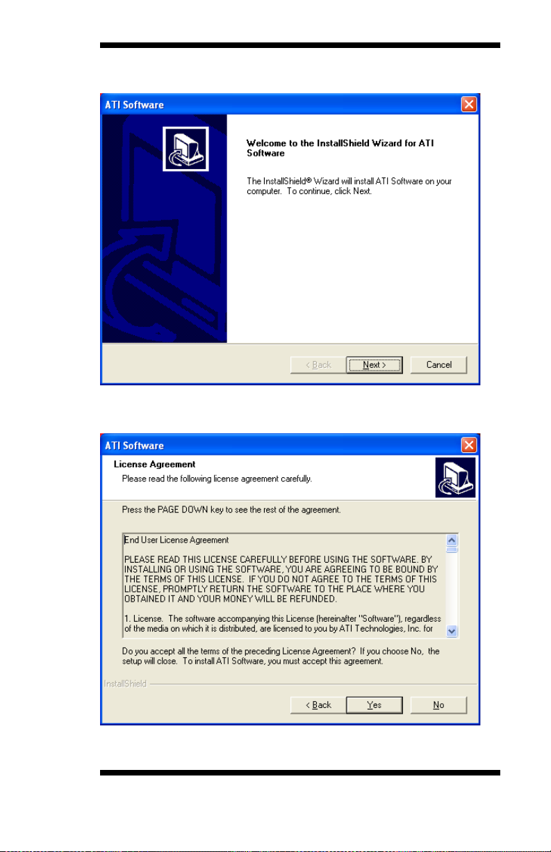
3. When the Welcome screen appears, click Next to continue.
4. Click Yes to accept the software license agreement and proceed with
the installation process.
MB879 User’s Manual 49
Page 56

DRIVER INSTALLATION
5. The Setup process is now complete. Click Finish to restart the
computer and for changes to take effect. When the computer has
restarted, the system will be able to find some devices. Restart your
computer when prompted .
50 MB879 User’s Manual
Page 57

DRIVERS INSTALLATION
Realtek AC97 Codec Audio Driver Installation
Follow the steps below to install the Realtek AC97 Codec Audio
Drivers.
1. Insert the CD that comes with the board. Click ATI RC410MD
Chipset Drivers and then Realtek AC’97 Codec Audio Driver.
2. When the Welcome screen appears, click Next to continue.
MB879 User’s Manual 51
Page 58

DRIVER INSTALLATION
3. Click Finish to restart the computer and for changes to take effect. .
52 MB879 User’s Manual
Page 59
DRIVERS INSTALLATION
LAN Driver Installation
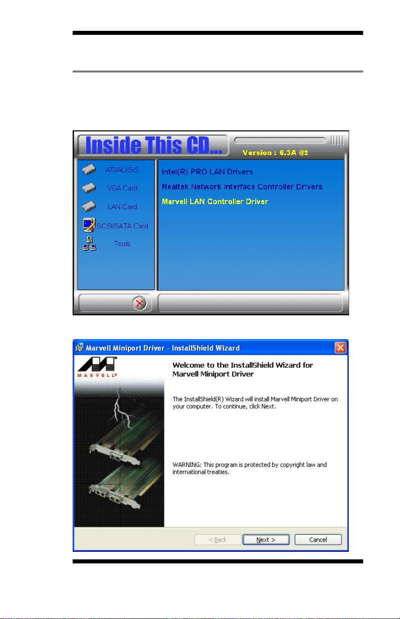
Follow the steps below to install the Marvell Gigabit LAN drivers.
1. Insert the CD that comes with the board. Click LAN Card and then
Marvell LAN Controller Driver.
2. Click Next when the InstallShield Wizard welcome screen appears.
MB879 User’s Manual 53
Page 60

DRIVER INSTALLATION
3. Click Next to agree with the license agreement. Click Next when
the Readme Information screen appears to proceed with the drives
installation process. When the Installation is complete, click Finish
for the changes to take effect.
54 MB879 User’s Manual
Page 61

DRIVERS INSTALLATION
4. To use the wake up function by PCIe LAN, go to the Device
Manager under Windows and select LAN controller. The following
window will appear (Generic Marvell Yukon Chipset based Ethernet
Controller Properties). Click Advanced and select Wake From
Shutdown. In the Value field on the right, select On.
5. Then, also in the Advanced section, click on Wake Up Capabilities.
In the Value field on the right, select Magic Packet, then click OK.
MB879 User’s Manual 55
Page 62

DRIVER INSTALLATION
This page is intentionally left blank.
56 MB879 User’s Manual
Page 63

APPENDIX
Appendix
A. I/O Port Address Map
Each peripheral device in the system is assigned a set of I/O port
addresses which also becomes the identity of the device. The following
table lists the I/O port addresses used.
Address Device Description
000h - 01Fh DMA Controller #1
020h - 03Fh Interrupt Controller #1
040h - 05Fh Timer
060h - 06Fh Keyboard Controller
070h - 07Fh Real Time Clock, NMI
080h - 09Fh DMA Page Register
0A0h - 0BFh Interrupt Controller #2
0C0h - 0DFh DMA Controller #2
0F0h Clear Math Coprocessor Busy Signal
0F1h Reset Math Coprocessor
1F0h - 1F7h IDE Interface
278 - 27F Parallel Port #2(LPT2)
2F8h - 2FFh Serial Port #2(COM2)
2B0 - 2DF Graphics adapter Controller
378h - 3FFh Parallel Port #1(LPT1)
360 - 36F Network Ports
3B0 - 3BF Monochrome & Printer adapter
3C0 - 3CF EGA adapter
3D0 - 3DF CGA adapter
3F0h - 3F7h Floppy Disk Controller
3F8h - 3FFh Serial Port #1(COM1)
MB879 User’s Manual 57
Page 64

APPENDIX
B. Interrupt Request Lines (IRQ)
Peripheral devices use interrupt request lines to notify CPU for the
service required. The following table shows the IRQ used by the
devices on board.
Level Function
IRQ0 System Timer Output
IRQ1 Keyboard
IRQ2 Interrupt Cascade
IRQ3 Serial Port #2
IRQ4 Serial Port #1
IRQ5 Reserved
IRQ6 Floppy Disk Controller
IRQ7 Parallel Port #1
IRQ8 Real Time Clock
IRQ9 Reserved
IRQ10 Reserved
IRQ11 Reserved
IRQ12 PS/2 Mouse
IRQ13 80287
IRQ14 Primary IDE
IRQ15 Secondary IDE
58 MB879 User’s Manual
Page 65

APPENDIX
C. Watchdog Timer Configuration
The WDT is used to generate a variety of output signals after a user
programmable count. The WDT is suitable for use in the prevention of
system lock-up, such as when software becomes trapped in a deadlock.
Under these sorts of circumstances, the timer will count to zero and
the selected outputs will be driven. Under normal circumstance, the
user will restart the WDT at regular intervals before the timer counts
to zero.
SAMPLE CODE:
File : ITE8712.H
//=======================================================================
//
// THIS CODE AND INFORMATION IS PROVIDED "AS IS" WITHOUT WARRANTY OF ANY
// KIND, EITHER EXPRESSED OR IMPLIED, INCLUDING BUT NOT LIMITED TO THE
// IMPLIED WARRANTIES OF MERCHANTABILITY AND/OR FITNESS FOR A PARTICULAR
// PURPOSE.
//
//=======================================================================
#ifndef __ITE8712_H
#define __ITE8712_H 1
//=======================================================================
#define ITE8712_INDEX_PORT (ITE8712_BASE)
#define ITE8712_DATA_PORT (ITE8712_BASE+1)
//=======================================================================
#define ITE8712_REG_LD 0x07
//=======================================================================
//=======================================================================
#define ITE8712_IO_PORT 0x0803
//=======================================================================
#define ITE8712_UNLOCK1 0x87
#define ITE8712_UNLOCK2 0x01
#define ITE8712_UNLOCK3 0x55
#define ITE8712_UNLOCK4 0xAA
#define ITE8712_LOCK 0xFF
//=======================================================================
unsigned int Init_ITE8712(void);
void Set_ITE8712_LD( unsigned char);
void Set_ITE8712_Reg( unsigned char, unsigned char);
unsigned char Get_ITE8712_Reg( unsigned char);
//=======================================================================
#endif//__ITE8712_H
MB879 User’s Manual 59
Page 66

APPENDIX
File : ITE8712.CPP
//=======================================================================
//
// THIS CODE AND INFORMATION IS PROVIDED "AS IS" WITHOUT WARRANTY OF ANY
// KIND, EITHER EXPRESSED OR IMPLIED, INCLUDING BUT NOT LIMITED TO THE
// IMPLIED WARRANTIES OF MERCHANTABILITY AND/OR FITNESS FOR A PARTICULAR
// PURPOSE.
//
//=======================================================================
#include "ITE8712.H"
#include <dos.h>
//=======================================================================
unsigned int ITE8712_BASE;
void Unlock_ITE8712 (void);
void Lock_ITE8712 (void);
//=======================================================================
unsigned int Init_ITE8712(void)
{
unsigned int result; //0=NA,1=ITE8712
ITE8712_BASE = 0x2E;
result = Get_ITE8712_Reg(0x21);
if (result == 0x12)
{
result = 1;
goto Init_Finish;
}
ITE8712_BASE = 0x4E;
result = Get_ITE8712_Reg(0x21);
if (result == 0x12)
{
result = 1;
goto Init_Finish;
}
ITE8712_BASE = 0x00;
result = 0;
Init_Finish:
return (result);
}
//=======================================================================
void Unlock_ITE8712 (void)
{
outportb(ITE8712_INDEX_PORT, ITE8712_UNLOCK1);
outportb(ITE8712_INDEX_PORT, ITE8712_UNLOCK2);
outportb(ITE8712_INDEX_PORT, ITE8712_UNLOCK3);
if (ITE8712_BASE == 0x2E)
outportb(ITE8712_INDEX_PORT, ITE8712_UNLOCK3);
else
outportb(ITE8712_INDEX_PORT, ITE8712_UNLOCK4);
}
//=======================================================================
void Lock_ITE8712 (void)
{
outportb(ITE8712_INDEX_PORT, ITE8712_LOCK);
60 MB879 User’s Manual
Page 67

APPENDIX
}
//=======================================================================
void Set_ITE8712_LD( unsigned char LD)
{
Unlock_ITE8712();
outportb(ITE8712_INDEX_PORT, ITE8712_REG_LD);
outportb(ITE8712_DATA_PORT, LD);
Lock_ITE8712();
}
//=======================================================================
void Set_ITE8712_Reg( unsigned char REG, unsigned char DATA)
{
Unlock_ITE8712();
outportb(ITE8712_INDEX_PORT, REG);
outportb(ITE8712_DATA_PORT, DATA);
Lock_ITE8712();
}
//=======================================================================
unsigned char Get_ITE8712_Reg(unsigned char REG)
{
unsigned char Result;
Unlock_ITE8712();
outportb(ITE8712_INDEX_PORT, REG);
Result = inportb(ITE8712_DATA_PORT);
Lock_ITE8712();
return Result;
}
//=======================================================================
File : Main.cpp
//=======================================================================
//
// THIS CODE AND INFORMATION IS PROVIDED "AS IS" WITHOUT WARRANTY OF ANY
// KIND, EITHER EXPRESSED OR IMPLIED, INCLUDING BUT NOT LIMITED TO THE
// IMPLIED WARRANTIES OF MERCHANTABILITY AND/OR FITNESS FOR A PARTICULAR
// PURPOSE.
//
//=======================================================================
#include <stdio.h>
#include <stdlib.h>
#include "ITE8712.H"
//=======================================================================
int main (int argc, char *argv[]);
void copyright(void);
void EnableWDT(int);
void DisableWDT(void);
//=======================================================================
int main (int argc, char *argv[])
{
unsigned char bTime;
char **endptr;
copyright();
if (argc != 2)
{
printf(" Parameter incorrect!!\n");
MB879 User’s Manual 61
Page 68

APPENDIX
return 1;
}
if (Init_ITE8712() == 0)
{
printf(" ITE8712 is not detected, program abort.\n");
return 1;
}
bTime = strtol (argv[1], endptr, 10);
if (bTime == 0)
{
printf("Watch Dog Timer is disabled !!\n", bTime);
DisableWDT();
}
else
{
printf("System will reset after %d seconds\n", bTime);
EnableWDT(bTime);
}
return 0;
}
//=======================================================================
void copyright(void)
{
printf("\n======== ITE8712 Watch Timer Tester (AUTO DETECT) ========\n"\
}
//=======================================================================
void EnableWDT(int interval)
{
Set_ITE8712_LD(0x07); //Set Logic Device 7
Set_ITE8712_Reg(0x72, 0xC0); //Enable WDT
Set_ITE8712_Reg(0x73, interval); //set timer
}
//=======================================================================
void DisableWDT(void)
{
Set_ITE8712_LD(0x07); //switch to logic device 7
Set_ITE8712_Reg(0x72, 0x00); //watchdog disabled
Set_ITE8712_Reg(0x73, 0x00); //Clear watchdog timer
}
//=======================================================================
" Usage : ITE8712 reset_time Unit\n"\
" Ex : ITE8712 3 => reset system after 3 Seconds\n"\
" ITE8712 0 => disable watch dog timer\n");
62 MB879 User’s Manual
 Loading...