

Page 1

Intel® MAX® 10 General Purpose I/O
User Guide
Updated for Intel® Quartus® Prime Design Suite: 20.1
Subscribe
Send Feedback
UG-M10GPIO | 2021.04.27
Latest document on the web: PDF | HTML
Page 2

Contents
Contents
1. Intel® MAX® 10 I/O Overview.........................................................................................3
1.1. Intel MAX 10 Devices I/O Resources Per Package ..................................................... 4
1.2. Intel MAX 10 I/O Vertical Migration Support.............................................................. 5
2. Intel MAX 10 I/O Architecture and Features..................................................................6
2.1. Intel MAX 10 I/O Standards Support........................................................................ 6
2.1.1. Intel MAX 10 I/O Standards Voltage and Pin Support......................................9
2.2. Intel MAX 10 I/O Elements....................................................................................12
2.2.1. Intel MAX 10 I/O Banks Architecture...........................................................13
2.2.2. Intel MAX 10 I/O Banks Performance..........................................................14
2.2.3. Intel MAX 10 I/O Banks Locations.............................................................. 14
2.3. Intel MAX 10 I/O Buffers.......................................................................................17
2.3.1. Schmitt-Trigger Input Buffer...................................................................... 17
2.3.2. Programmable I/O Buffer Features............................................................. 17
2.4. I/O Standards Termination.................................................................................... 25
2.4.1. Voltage-Referenced I/O Standards Termination............................................ 25
2.4.2. Differential I/O Standards Termination........................................................ 26
2.4.3. Intel MAX 10 On-Chip I/O Termination........................................................ 27
3. Intel MAX 10 I/O Design Considerations...................................................................... 30
3.1. Guidelines: V
Range Considerations.................................................................. 30
CCIO
3.2. Guidelines: Voltage-Referenced I/O Standards Restriction......................................... 31
3.3. Guidelines: Enable Clamp Diode for LVTTL/LVCMOS Input Buffers...............................31
3.4. Guidelines: Adhere to the LVDS I/O Restrictions Rules.............................................. 32
3.5. Guidelines: I/O Restriction Rules............................................................................32
3.6. Guidelines: Placement Restrictions for 1.0 V I/O Pin................................................. 33
3.6.1. Calculating the Total Inductance for 1.0 V Pin Placement............................... 33
3.7. Guidelines: Analog-to-Digital Converter I/O Restriction............................................. 35
3.8. Guidelines: External Memory Interface I/O Restrictions.............................................38
3.9. Guidelines: Dual-Purpose Configuration Pin............................................................. 38
3.10. Guidelines: Clock and Data Input Signal for Intel MAX 10 E144 Package.................... 39
4. Intel MAX 10 I/O Implementation Guides.....................................................................41
4.1. GPIO Lite Intel FPGA IP........................................................................................ 41
4.1.1. GPIO Lite Intel FPGA IP Data Paths.............................................................42
4.2. Verifying Pin Migration Compatibility.......................................................................44
5. GPIO Lite Intel FPGA IP References.............................................................................. 46
5.1. GPIO Lite Intel FPGA IP Parameter Settings.............................................................46
5.2. GPIO Lite Intel FPGA IP Interface Signals................................................................ 48
6. Intel MAX 10 General Purpose I/O User Guide Archives............................................... 50
7. Document Revision History for Intel MAX 10 General Purpose I/O User Guide............. 51
Intel® MAX® 10 General Purpose I/O User Guide
2
Send Feedback
Page 3

UG-M10GPIO | 2021.04.27
Send Feedback
1. Intel® MAX® 10 I/O Overview
The Intel® MAX® 10 general purpose I/O (GPIO) system consists of the I/O elements
(IOE) and the GPIO Lite Intel FPGA IP. You can use GPIOs in non-transceiver general
applications, memory-like interfaces, or LVDS applications.
• The IOEs contain bidirectional I/O buffers and I/O registers located in I/O banks
around the periphery of the device.
• The GPIO Lite IP core supports the GPIO components and features, including
double data rate I/O (DDIO), delay chains, I/O buffers, control signals, and
clocking.
Related Information
• Intel MAX 10 I/O Architecture and Features on page 6
Provides information about the architecture and features of the I/Os in Intel
MAX 10 devices.
• Intel MAX 10 I/O Design Considerations on page 30
Provides I/O design guidelines for Intel MAX 10 Devices.
• Intel MAX 10 I/O Implementation Guides on page 41
Provides guides to implement I/Os in Intel MAX 10 Devices.
• GPIO Lite Intel FPGA IP References on page 46
Lists the parameters and signals of GPIO Lite IP core for Intel MAX 10 Devices.
• Intel MAX 10 General Purpose I/O User Guide Archives on page 50
Provides a list of user guides for previous versions of the GPIO Lite IP core.
Intel Corporation. All rights reserved. Agilex, Altera, Arria, Cyclone, eASIC, Intel, the Intel logo, MAX, Nios,
Quartus and Stratix words and logos are trademarks of Intel Corporation or its subsidiaries in the U.S. and/or
other countries. Intel warrants performance of its FPGA and semiconductor products to current specifications in
accordance with Intel's standard warranty, but reserves the right to make changes to any products and services
at any time without notice. Intel assumes no responsibility or liability arising out of the application or use of any
information, product, or service described herein except as expressly agreed to in writing by Intel. Intel
customers are advised to obtain the latest version of device specifications before relying on any published
information and before placing orders for products or services.
*Other names and brands may be claimed as the property of others.
ISO
9001:2015
Registered
Page 4
®
1. Intel
MAX® 10 I/O Overview
UG-M10GPIO | 2021.04.27
1.1. Intel MAX 10 Devices I/O Resources Per Package
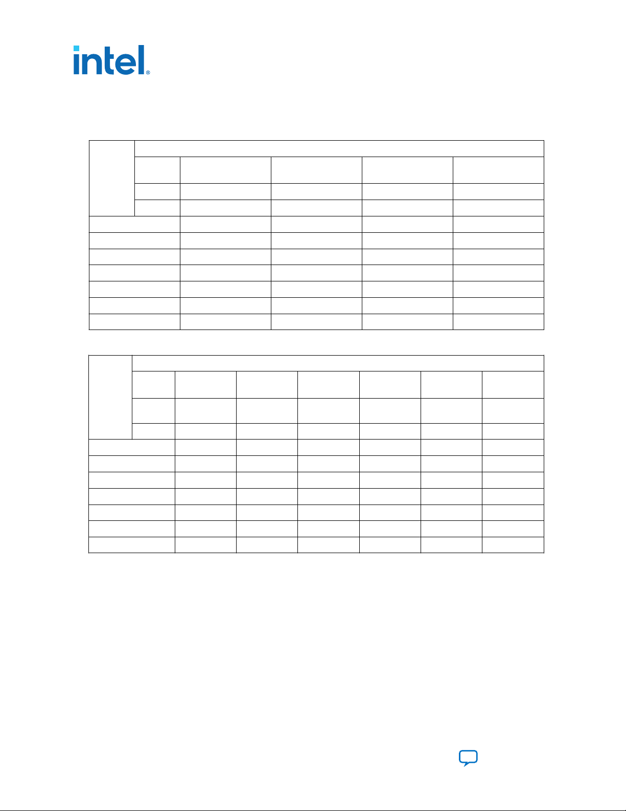
Table 1. Package Plan for Intel MAX 10 Single Power Supply Devices
Device Package
Type M153
153-pin MBGA
Size 8 mm × 8 mm 11 mm × 11 mm 15 mm × 15 mm 22 mm × 22 mm
Ball Pitch 0.5 mm 0.8 mm 0.8 mm 0.5 mm
10M02 112 130 246 101
10M04 112 130 246 101
10M08 112 130 246 101
10M16 — 130 246 101
10M25 — — — 101
10M40 — — — 101
10M50 — — — 101
Table 2. Package Plan for Intel MAX 10 Dual Power Supply Devices
U169
169-pin UBGA
U324
324-pin UBGA
E144
144-pin EQFP
Device Package
Type V36
36-pin WLCSP
Size 3 mm × 3 mm 4 mm × 4 mm 15 mm × 15mm17 mm × 17mm23 mm × 23mm27 mm × 27
Ball Pitch 0.4 mm 0.4 mm 0.8 mm 1.0 mm 1.0 mm 1.0 mm
10M02 27 — 160 — — —
10M04 — — 246 178 — —
10M08 — 56 246 178 250 —
10M16 — — 246 178 320 —
10M25 — — — 178 360 —
10M40 — — — 178 360 500
10M50 — — — 178 360 500
V81
81-pin WLCSP
U324
324-pin UBGA
F256
256-pin FBGA
F484
484-pin FBGA
F672
672-pin FBGA
mm
Related Information
Development Kits and Boards, Intel MAX Design Tools
Intel® MAX® 10 General Purpose I/O User Guide
4
Send Feedback
Page 5
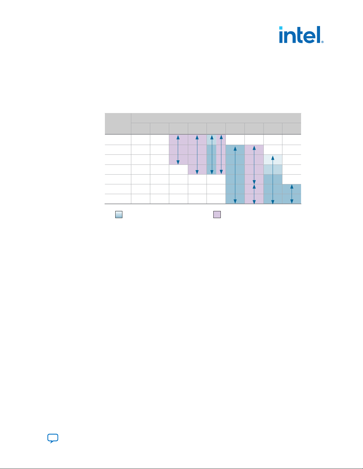
Device
V36 V81 M153 U169 U324 F256 E144 F484 F672
10M02
10M04
10M08
10M16
10M25
10M40
10M50
Package
Single Power Supply Devices
Dual Power Supply Devices
®
1. Intel
UG-M10GPIO | 2021.04.27
MAX® 10 I/O Overview
1.2. Intel MAX 10 I/O Vertical Migration Support
Figure 1. Migration Capability Across Intel MAX 10 Devices
• The arrows indicate the migration paths. The devices included in each vertical migration path are shaded.
Non-migratable devices are omitted. Some packages have several migration paths. Devices with lesser
I/O resources in the same path have lighter shades.
• To achieve the full I/O migration across product lines in the same migration path, restrict I/Os usage to
match the product line with the lowest I/O count.
Note: Before starting migration work, Intel recommends that you verify the pin migration
compatibility through the Pin Migration View window in the Intel Quartus® Prime
software Pin Planner. For example, not all Intel MAX 10 devices support 1.0 V I/O.
Related Information
Verifying Pin Migration Compatibility on page 44
Send Feedback
Intel® MAX® 10 General Purpose I/O User Guide
5
Page 6

UG-M10GPIO | 2021.04.27
Send Feedback
2. Intel MAX 10 I/O Architecture and Features
The I/O system of Intel MAX 10 devices support various I/O standards. In the Intel
MAX 10 devices, the I/O pins are located in I/O banks at the periphery of the devices.
The I/O pins and I/O buffers have several programmable features.
Related Information
Intel MAX 10 I/O Overview on page 3
2.1. Intel MAX 10 I/O Standards Support
Intel MAX 10 devices support a wide range of I/O standards, including single-ended,
voltage-referenced single-ended, and differential I/O standards.
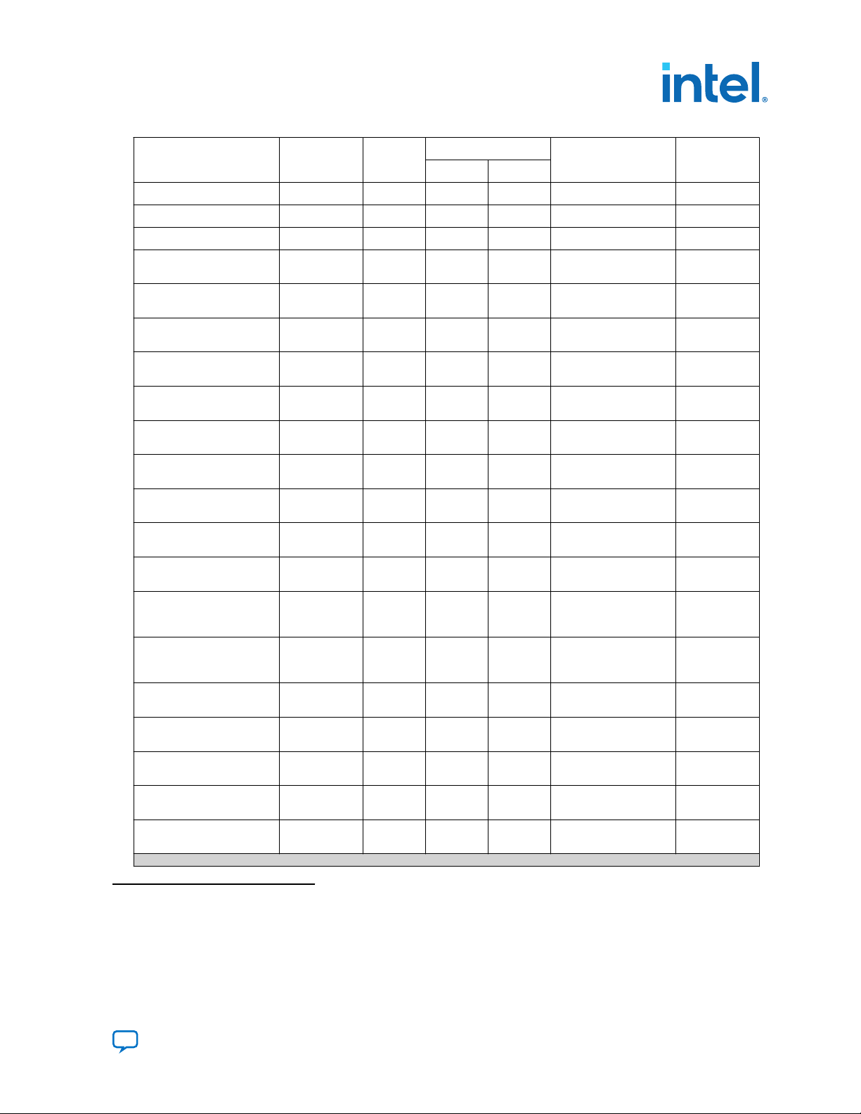
Table 3. Supported I/O Standards in Intel MAX 10 Devices
The voltage-referenced I/O standards are not supported in the following I/O banks of these device packages:
• All I/O banks of V36 package of 10M02.
• All I/O banks of V81 package of 10M08.
• Banks 1A and 1B of E144 package of 10M50.
I/O Standard
3.3 V LVTTL/3.3 V
LVCMOS
3.0 V LVTTL/3.0 V
LVCMOS
2.5 V LVCMOS Single-ended All Yes Yes General purpose JESD8-5
1.8 V LVCMOS Single-ended All Yes Yes General purpose JESD8-7
1.5 V LVCMOS Single-ended All Yes Yes General purpose JESD8-11
1.2 V LVCMOS Single-ended All Yes Yes General purpose JESD8-12
1.0 V LVCMOS
3.0 V PCI Single-ended All Yes Yes General purpose PCI Rev. 2.2
3.3 V Schmitt Trigger Single-ended All Yes — General purpose —
(1)
Available only for the following devices: 10M02SCU324C8G, 10M04SCU324C8G,
(1)
Type Device
Single-ended All Yes Yes General purpose JESD8-B
Single-ended All Yes Yes General purpose JESD8-B
Single-ended Specific
Support
devices
(1)
Direction Application Standard
Input Output
Yes Yes General purpose —
continued...
Support
10M08SCU324C8G, 10M16SCU324C8G, 10M16SCU169C8G, 10M16SAU169C8G,
10M16DCF484C8G, 10M16DAF484C8G, 10M25DCF484C8G, 10M25DAF484C8G,
10M40DCF484C8G, 10M40DAF484C8G, 10M50DCF484C8G, and 10M50DAF484C8G.
Intel Corporation. All rights reserved. Agilex, Altera, Arria, Cyclone, eASIC, Intel, the Intel logo, MAX, Nios,
Quartus and Stratix words and logos are trademarks of Intel Corporation or its subsidiaries in the U.S. and/or
other countries. Intel warrants performance of its FPGA and semiconductor products to current specifications in
accordance with Intel's standard warranty, but reserves the right to make changes to any products and services
at any time without notice. Intel assumes no responsibility or liability arising out of the application or use of any
information, product, or service described herein except as expressly agreed to in writing by Intel. Intel
customers are advised to obtain the latest version of device specifications before relying on any published
information and before placing orders for products or services.
*Other names and brands may be claimed as the property of others.
ISO
9001:2015
Registered
Page 7
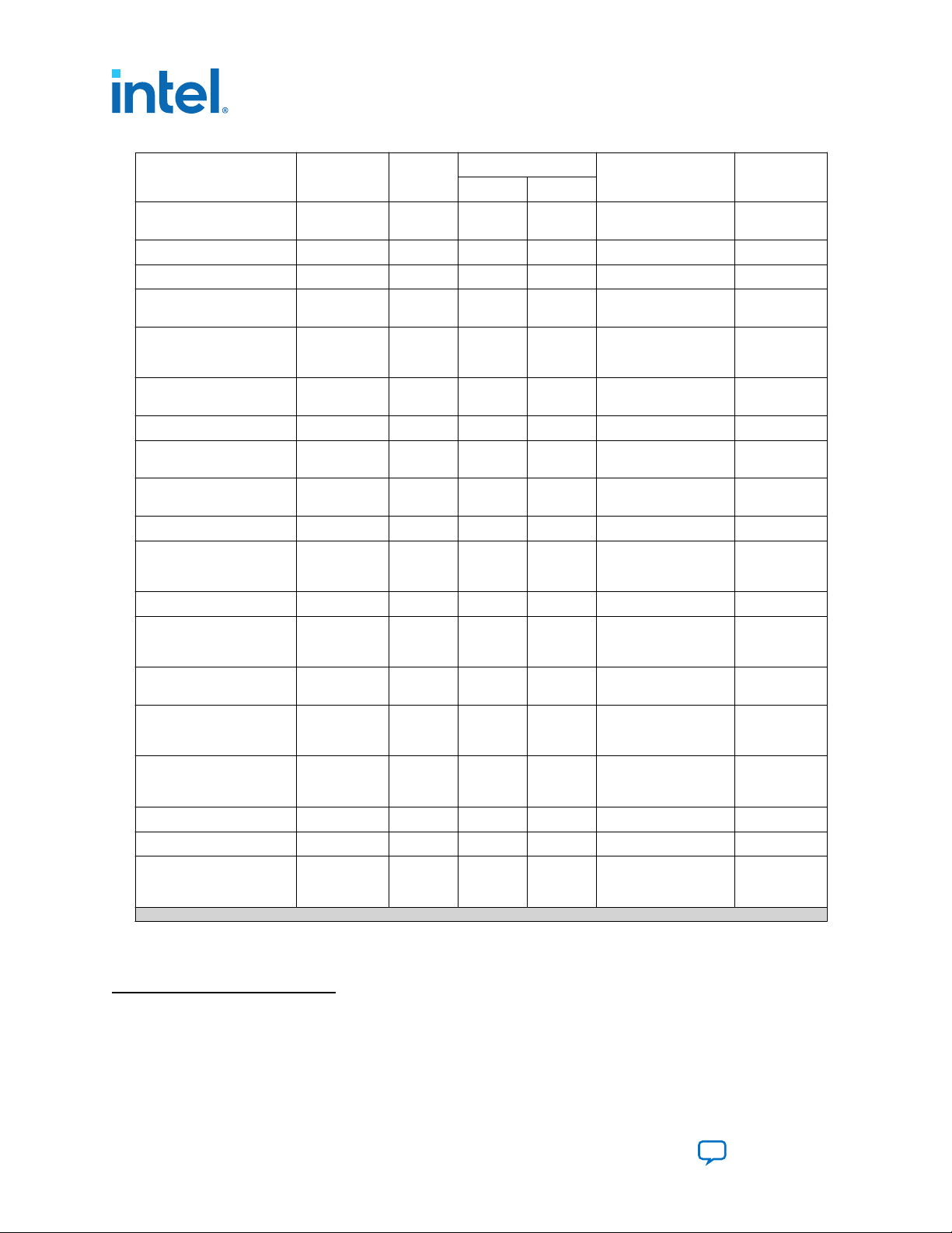
2. Intel MAX 10 I/O Architecture and Features
UG-M10GPIO | 2021.04.27
I/O Standard Type Device
Support
Direction Application Standard
Input Output
Support
2.5 V Schmitt Trigger Single-ended All Yes — General purpose —
1.8 V Schmitt Trigger Single-ended All Yes — General purpose —
1.5 V Schmitt Trigger Single-ended All Yes — General purpose —
SSTL-2 Class I Voltage-
All Yes Yes DDR1 JESD8-9B
referenced
SSTL-2 Class II Voltage-
All Yes Yes DDR1 JESD8-9B
referenced
SSTL-18 Class I Voltage-
All Yes Yes DDR2 JESD8-15
referenced
SSTL-18 Class II Voltage-
All Yes Yes DDR2 JESD8-15
referenced
SSTL-15 Class I Voltage-
All Yes Yes DDR3 —
referenced
SSTL-15 Class II Voltage-
All Yes Yes DDR3 —
referenced
(2)
SSTL-15
Voltage-
All Yes Yes DDR3 JESD79-3D
referenced
SSTL-135
(2)
Voltage-
All Yes Yes DDR3L —
referenced
1.8 V HSTL Class I Voltagereferenced
1.8 V HSTL Class II Voltagereferenced
1.5 V HSTL Class I Voltagereferenced
All Yes Yes DDR II+, QDR II+,
and RLDRAM 2
All Yes Yes DDR II+, QDR II+,
and RLDRAM 2
All Yes Yes DDR II+, QDR II+,
QDR II, and
JESD8-6
JESD8-6
JESD8-6
RLDRAM 2
1.5 V HSTL Class II Voltagereferenced
All Yes Yes DDR II+, QDR II+,
QDR II, and
JESD8-6
RLDRAM 2
1.2 V HSTL Class I Voltage-
All Yes Yes General purpose JESD8-16A
referenced
1.2 V HSTL Class II Voltage-
All Yes Yes General purpose JESD8-16A
referenced
HSUL-12
(2)
Voltage-
All Yes Yes LPDDR2 —
referenced
Differential SSTL-2 Class I
Differential All Yes
(3)
Yes
(4)
DDR1 JESD8-9B
and II
Differential SSTL-18 Class
Differential All Yes
(3)
Yes
(4)
DDR2 JESD8-15
I and Class II
continued...
(2)
Available in Intel MAX 10 16, 25, 40, and 50 devices only.
(3)
The inputs treat differential inputs as two single-ended inputs and decode only one of them.
(4)
The outputs use two single-ended output buffers with the second output buffer programmed
as inverted.
Send Feedback
Intel® MAX® 10 General Purpose I/O User Guide
7
Page 8
2. Intel MAX 10 I/O Architecture and Features
UG-M10GPIO | 2021.04.27
I/O Standard Type Device
Differential SSTL-15 Class
Differential All Yes
Support
Direction Application Standard
Input Output
(3)
Yes
(4)
DDR3 —
Support
I and Class II
Differential SSTL-15 Differential All Yes
Differential SSTL-135 Differential All Yes
Differential 1.8 V HSTL
Differential All Yes
Class I and Class II
Differential 1.5 V HSTL
Differential All Yes
Class I and Class II
(3)
(3)
(3)
(3)
Yes
Yes
Yes
Yes
(4)
(4)
(4)
(4)
DDR3 JESD79-3D
DDR3L —
DDR II+, QDR II+,
and RLDRAM 2
DDR II+, QDR II+,
QDR II, and
JESD8-6
JESD8-6
RLDRAM 2
Differential 1.2 V HSTL
Differential All Yes
(3)
Yes
(4)
General purpose JESD8-16A
Class I and Class II
Differential HSUL-12 Differential All Yes
LVDS (dedicated)
(5)
Differential All Yes Yes — ANSI/TIA/
(3)
Yes
(4)
LPDDR2 —
EIA-644
LVDS (emulated, external
resistors)
Mini-LVDS (dedicated)
(5)
Mini-LVDS (emulated,
external resistor)
Differential All — Yes — ANSI/TIA/
EIA-644
Differential All — Yes — —
Differential Dual
— Yes — —
supply
devices
RSDS (dedicated)
RSDS (emulated, external
resistor, 1R)
(5)
Differential All — Yes — —
Differential Dual
— Yes — —
supply
devices
RSDS (emulated, external
Differential All — Yes — —
resistors, 3R)
PPDS (dedicated)
(5)
Differential Dual
— Yes — —
supply
devices
PPDS (emulated, external
resistor)
Differential Dual
supply
— Yes — —
devices
LVPECL Differential All Yes — — —
Bus LVDS Differential All Yes Yes
TMDS Differential Dual
Yes — — —
(6)
— —
supply
devices
continued...
(5)
You can use dedicated LVDS transmitters only on the bottom I/O banks. You can use LVDS
receivers on all I/O banks.
(6)
The outputs use two single-ended output buffers with the second output buffer programmed
as inverted. A single series resistor is required.
Intel® MAX® 10 General Purpose I/O User Guide
8
Send Feedback
Page 9
2. Intel MAX 10 I/O Architecture and Features
UG-M10GPIO | 2021.04.27
I/O Standard Type Device
Support
Sub-LVDS Differential Dual
supply
devices
SLVS Differential Dual
supply
devices
HiSpi Differential Dual
supply
devices
Direction Application Standard
Input Output
Yes Yes
Yes Yes
Yes — — —
(7)
(8)
— —
— —
Related Information
• Intel MAX 10 I/O Buffers on page 17
Provides more information about available I/O buffer types and supported I/O
standards.
• LVDS Transmitter I/O Termination Schemes, Intel MAX 10 High-Speed LVDS I/O
User Guide
Provides the required external termination schemes and resistor values for the
emulated LVDS, Sub-LVDS, SLVS, emulated RSDS, emulated mini-LVDS, and
emulated PPDS I/O standards.
2.1.1. Intel MAX 10 I/O Standards Voltage and Pin Support
Table 4. Intel MAX 10 I/O Standards Voltage Levels and Pin Support
Support
Note: The I/O standards that each pin type supports depends on the I/O standards that the pin's
I/O Standard V
3.3 V LVTTL/3.3 V
LVCMOS
3.0 V LVTTL/3.0 V
LVCMOS
2.5 V LVCMOS 3.0/2.5 2.5 — Yes Yes Yes Yes Yes
1.8 V LVCMOS 1.8/1.5 1.8 — Yes Yes Yes Yes Yes
1.5 V LVCMOS 1.8/1.5 1.5 — Yes Yes Yes Yes Yes
1.2 V LVCMOS 1.2 1.2 — Yes Yes Yes Yes Yes
1.0 V LVCMOS 1.0
(7)
Requires external termination resistors.
(8)
The outputs uses two single-ended output buffers as emulated differential outputs. Requires
I/O bank supports. For example, only the bottom I/O banks support the LVDS (dedicated)
I/O standard. You can use the LVDS (dedicated) I/O standard for the PLL_CLKOUT pin only if
the pin is available in your device's bottom I/O banks. To determine the pin's I/O bank
locations for your device, check your device's pin out file.
(V) V
CCIO
Input Output
3.3/3.0/2.
5
3.0/2.5 3.0 — Yes Yes Yes Yes Yes
(9)
3.3 — Yes Yes Yes Yes Yes
(9)
1.0
(V) Pin Type Support
REF
PLL_CLKOUTMEM_CLK CLK DQS
— — — Yes — Yes
continued...
external termination resistors.
User
I/O
Send Feedback
Intel® MAX® 10 General Purpose I/O User Guide
9
Page 10

2. Intel MAX 10 I/O Architecture and Features
UG-M10GPIO | 2021.04.27
I/O Standard V
Input Output
(V) V
CCIO
(V) Pin Type Support
REF
PLL_CLKOUTMEM_CLK CLK DQS
User
I/O
3.0 V PCI 3.0 3.0 — Yes Yes Yes Yes Yes
3.3 V Schmitt Trigger 3.3 — — — — Yes Yes
2.5 V Schmitt Trigger 2.5 — — — — Yes Yes
1.8 V Schmitt Trigger 1.8 — — — — Yes Yes
1.5 V Schmitt Trigger 1.5 — — — — Yes Yes
(10)
(10)
(10)
(10)
Yes
Yes
Yes
Yes
SSTL-2 Class I 2.5 2.5 1.25 Yes Yes Yes Yes Yes
SSTL-2 Class II 2.5 2.5 1.25 Yes Yes Yes Yes Yes
SSTL-18 Class I 1.8 1.8 0.9 Yes Yes Yes Yes Yes
SSTL-18 Class II 1.8 1.8 0.9 Yes Yes Yes Yes Yes
SSTL-15 Class I 1.5 1.5 0.75 Yes Yes Yes Yes Yes
SSTL-15 Class II 1.5 1.5 0.75 Yes Yes Yes Yes Yes
SSTL-15 1.5 1.5 0.75 Yes Yes Yes Yes Yes
SSTL-135 1.35 1.35 0.675 Yes Yes Yes Yes Yes
1.8 V HSTL Class I 1.8 1.8 0.9 Yes Yes Yes Yes Yes
1.8 V HSTL Class II 1.8 1.8 0.9 Yes Yes Yes Yes Yes
1.5 V HSTL Class I 1.5 1.5 0.75 Yes Yes Yes Yes Yes
1.5 V HSTL Class II 1.5 1.5 0.75 Yes Yes Yes Yes Yes
1.2 V HSTL Class I 1.2 1.2 0.6 Yes Yes Yes Yes Yes
1.2 V HSTL Class II 1.2 1.2 0.6 Yes Yes Yes Yes Yes
HSUL-12 1.2 1.2 0.6 Yes Yes Yes Yes Yes
Differential SSTL-2 Class
I and II
Differential SSTL-18
Class I and Class II
Differential SSTL-15
Class I and Class II
— 2.5 — Yes Yes — Yes —
2.5 — 1.25 — — Yes Yes —
— 1.8 — Yes Yes — Yes —
1.8 — 0.9 — — Yes Yes —
— 1.5 — Yes Yes — Yes —
1.5 — 0.75 — — Yes Yes —
Differential SSTL-15 — 1.5 — Yes Yes — Yes —
1.5 — 0.75 — — Yes Yes —
Differential SSTL-135 — 1.35 — Yes Yes — Yes —
1.35 — 0.675 — — Yes Yes —
Differential 1.8 V HSTL
— 1.8 — Yes Yes — Yes —
Class I and Class II
continued...
(9)
Not supported on bank 1B and bank 8.
(10)
Bidirectional—use Schmitt Trigger input with LVTTL output.
Intel® MAX® 10 General Purpose I/O User Guide
10
Send Feedback
Page 11

2. Intel MAX 10 I/O Architecture and Features
UG-M10GPIO | 2021.04.27
I/O Standard V
Input Output
1.8 — 0.9 — — Yes Yes —
Differential 1.5 V HSTL
Class I and Class II
Differential 1.2 V HSTL
Class I and Class II
Differential HSUL-12 — 1.2 — Yes Yes — Yes —
LVDS (dedicated) 2.5 2.5 — Yes Yes Yes — Yes
LVDS (emulated,
external resistors)
Mini-LVDS (dedicated) — 2.5 — Yes Yes — — Yes
Mini-LVDS (emulated,
external resistor)
RSDS (dedicated) — 2.5 — Yes Yes — — Yes
RSDS (emulated,
external resistor, 1R)
RSDS (emulated,
external resistors, 3R)
PPDS (dedicated) — 2.5 — Yes Yes — — Yes
PPDS (emulated,
external resistor)
LVPECL 2.5 — — — — Yes — —
Bus LVDS 2.5 2.5 — — — — — Yes
TMDS 2.5 — — — — Yes — Yes
Sub-LVDS 2.5 1.8 — Yes Yes Yes — Yes
SLVS 2.5 2.5 — Yes Yes Yes — Yes
HiSpi 2.5 — — — — Yes — Yes
1.5 — 0.75 — — Yes Yes —
1.2 — 0.6 — — Yes Yes —
1.2 — 0.6 — — Yes Yes —
(V) V
CCIO
— 1.5 — Yes Yes — Yes —
— 1.2 — Yes Yes — Yes —
— 2.5 — Yes Yes — — Yes
— 2.5 — Yes Yes — — Yes
— 2.5 — Yes Yes — — Yes
— 2.5 — Yes Yes — — Yes
— 2.5 — Yes Yes — — Yes
(V) Pin Type Support
REF
PLL_CLKOUTMEM_CLK CLK DQS
User
I/O
Related Information
• Intel MAX 10 Device Pin-Out Files
• Intel MAX 10 I/O Standards Support on page 6
• Intel MAX 10 I/O Banks Locations on page 14
• Intel MAX 10 LVDS SERDES I/O Standards Support
• Intel MAX 10 High-Speed LVDS I/O Location
Send Feedback
Intel® MAX® 10 General Purpose I/O User Guide
11
Page 12

2.2. Intel MAX 10 I/O Elements
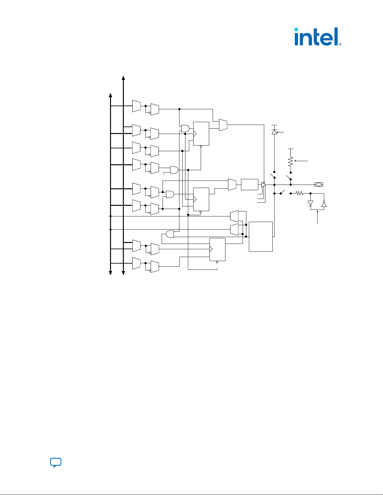
The Intel MAX 10 I/O elements (IOEs) contain a bidirectional I/O buffer and five
registers for registering input, output, output-enable signals, and complete embedded
bidirectional single data rate (SDR) and double data rate (DDR) transfer.
The I/O buffers are grouped into groups of four I/O modules per I/O bank:
•
The Intel MAX 10 devices share the user I/O pins with the VREF, RUP, RDN,
CLKPIN, PLLCLKOUT, configuration, and test pins.
• Schmitt Trigger input buffer is available in all I/O buffers.
• When the Intel MAX 10 device is blank or erased, the I/Os are tri-stated.
Each IOE contains one input register, two output registers, and two output-enable
(OE) registers:
• The two output registers and two OE registers are used for DDR applications.
• You can use the input registers for fast setup times and output registers for fast
clock-to-output times.
• You can use the OE registers for fast clock-to-output enable times.
You can use the IOEs for input, output, or bidirectional data paths. The I/O pins
support various single-ended and differential I/O standards.
2. Intel MAX 10 I/O Architecture and Features
UG-M10GPIO | 2021.04.27
Intel® MAX® 10 General Purpose I/O User Guide
12
Send Feedback
Page 13
D Q
ENA
D Q
ENA
V
CCIO
V
CCIO
Optional
PCI Clamp
Programmable
Pull-Up
Resistor
Bus Hold
Input Pin to
Input Register
Delay
or Input Pin to
Logic Array
Delay
Output
Pin Delay
clkin
oe_in
data_in0
data_in1
sclr/
preset
Chip-Wide Reset
aclr/prn
oe_out
clkout
OE
OE Register
Current Strength Control
Open-Drain Out
Column
or Row
Interconnect
io_clk[5..0]
Slew Rate Control
ACLR/PRN
ACLR/PRN
Output Register
D Q
ENA
ACLR/PRN
Input Register
2. Intel MAX 10 I/O Architecture and Features
UG-M10GPIO | 2021.04.27
Figure 2. IOE Structure in Bidirectional Configuration
Related Information
• Intel MAX 10 Power Management User Guide
Provides more information about the I/O buffers in different power cycles and
hot socketing.
• Schmitt-Trigger Input Buffer on page 17
2.2.1. Intel MAX 10 I/O Banks Architecture
Send Feedback
The I/O elements are located in a group of four modules per I/O bank:
• High speed DDR3 I/O banks—supports various I/O standards and protocols
including DDR3. These I/O banks are available only on the right side of the device.
• High speed I/O banks—supports various I/O standards and protocols except
DDR3. These I/O banks are available on the top, left, and bottom sides of the
device.
• Low speed I/O banks—lower speeds I/O banks that are located at the top left side
of the device.
For more information about I/O pins support, refer to the pinout files for your device.
Intel® MAX® 10 General Purpose I/O User Guide
13
Page 14

Related Information
Intel MAX 10 Device Pin-Out Files
2.2.2. Intel MAX 10 I/O Banks Performance
The performance of the I/O banks differs for different I/O standards and I/O bank
types. You must ensure that the frequency you specified passes timing check in the
Intel Quartus Prime software.
The low speed I/O banks have lower maximum frequency than other I/O banks
because of longer propagation delays. However, the delays do not affect the timing
parameters such as slew rate, rise time, and fall time.
For details about the location of the high speed and low speed I/O banks, refer to the
device pinout files.
Related Information
• High-Speed I/O Specifications
Provides the performance information for different I/O standards in the lowspeed and high-speed I/O banks.
• IBIS Models for Intel Devices
• SPICE Models for Altera Devices
2. Intel MAX 10 I/O Architecture and Features
UG-M10GPIO | 2021.04.27
2.2.3. Intel MAX 10 I/O Banks Locations
The I/O banks are located at the periphery of the device.
For more details about the modular I/O banks available in each device package, refer
to the relevant device pin-out file.
Intel® MAX® 10 General Purpose I/O User Guide
14
Send Feedback
Page 15

1
2
5
6
3
8
VREF1
VCCIO8VREF8
VCCIO1
VCCIO5VCCIO2
VCCIO3 VREF3
VCCIO6
VREF6
VREF2
VREF5
Low Speed I/O
High Speed I/O
1A
1B
2
5
6
3 4
8 7
VCCIO5VCCIO2
VCCIO3 VREF3 VREF4VCCIO4
VCCIO7VCCIO8
VCCIO1B
VCCIO1A
VCCIO6
VREF6
VREF1
VREF2
VREF8 VREF7
VREF5
Low Speed I/O
High Speed I/O
2. Intel MAX 10 I/O Architecture and Features
UG-M10GPIO | 2021.04.27
Figure 3. I/O Banks for 10M02 Devices (Except Single Power Supply U324 Package)
Figure 4. I/O Banks for 10M02 (Single Power Supply U324 Package), 10M04, and
10M08 Devices
Send Feedback
Intel® MAX® 10 General Purpose I/O User Guide
15
Page 16

1A
1B
2
5
6
3 4
8 7
VCCIO5VCCIO2
VCCIO3 VREF3 VREF4VCCIO4
VCCIO7VCCIO8
VCCIO1B
VCCIO1A
VCCIO6
VREF6
VREF1
VREF2
VREF8 VREF7
VREF5
Low Speed I/O
High Speed I/O
High Speed DDR3 I/O
OCT
2. Intel MAX 10 I/O Architecture and Features
Figure 5. I/O Banks for 10M16, 10M25 , 10M40, and 10M50 Devices
UG-M10GPIO | 2021.04.27
Related Information
• Intel MAX 10 Device Pin-Out Files
• High-Speed I/O Specifications
Provides the performance information for different I/O standards in the lowspeed and high-speed I/O banks.
Intel® MAX® 10 General Purpose I/O User Guide
16
Send Feedback
Page 17

2. Intel MAX 10 I/O Architecture and Features
UG-M10GPIO | 2021.04.27
2.3. Intel MAX 10 I/O Buffers
The general purpose I/Os (GPIOs) in Intel MAX 10 devices consist of LVDS I/O and
DDR I/O buffers.
Table 5. Types of GPIO Buffers in Intel MAX 10 Devices
LVDS I/O Buffers DDR I/O Buffers
• Support differential and single-ended I/O standards.
• Available only on I/O banks at the bottom side of the
device.
• For LVDS, the bottom I/O banks support LVDS
transmitter, emulated LVDS transmitter, and LVDS
receiver buffers.
Related Information
• Intel MAX 10 I/O Standards Support on page 6
• LVDS Transmitter I/O Termination Schemes, Intel MAX 10 High-Speed LVDS I/O
User Guide
Provides the required external termination schemes and resistor values for the
emulated LVDS, Sub-LVDS, SLVS, emulated RSDS, emulated mini-LVDS, and
emulated PPDS I/O standards.
• Support differential and single-ended I/O standards.
• Available on I/O banks at the left, right, and top sides of
the device.
• For LVDS, the DDR I/O buffers support only LVDS
receiver and emulated LVDS transmitter buffers.
• For DDR, only the DDR I/O buffers on the right side of
the device supports DDR3 external memory interfaces.
DDR3 support is only available for Intel MAX 10 16, 25,
40, and 50 devices.
2.3.1. Schmitt-Trigger Input Buffer
The Intel MAX 10 devices feature selectable Schmitt trigger input buffer on all I/O
banks.
The Schmitt trigger input buffer has similar VIL and VIH as the LVTTL I/O standard but
with better noise immunity. The Schmitt trigger input buffers are used as default input
buffers during configuration mode.
Related Information
Intel MAX 10 Device Datasheet
2.3.2. Programmable I/O Buffer Features
The Intel MAX 10 I/O buffers support a range of programmable features. These
features increase the flexibility of I/O utilization and provide an alternative to reduce
the usage of external discrete components such as a pull-up resistor and a diode.
Table 6. Summary of Supported Intel MAX 10 Programmable I/O Buffer Features and
Settings
Feature Setting Condition Assignment Name Supported I/O Standards
Open Drain On, Off (default) To enable this
feature, use
the OPNDRN
primitive.
— • 3.0 V and 3.3 V LVTTL
• 1.0 V, 1.2 V, 1.5 V, 1.8 V, 2.5 V,
3.0 V, and 3.3 V LVCMOS
• SSTL-2, SSTL-18, SSTL-15, and
SSTL-135
continued...
Send Feedback
Intel® MAX® 10 General Purpose I/O User Guide
17
Page 18

2. Intel MAX 10 I/O Architecture and Features
UG-M10GPIO | 2021.04.27
Feature Setting Condition Assignment Name Supported I/O Standards
• 1.2 V, 1.5 V, and 1.8 V HSTL
• HSUL-12
• 3.0 V PCI
Bus-Hold On, Off (default) Disabled if you
Pull-up Resistor On, Off (default) Disabled if you
Slew Rate
Control
PCI Clamp
Diode
Pre-Emphasis 0 (disabled), 1
Differential
Output Voltage
0 (Slow), 1 (Medium),
2 (Fast). Default is 2.
On (default for input
pins),
Off (default for output
pins, except 3.0 V PCI)
(enabled). Default is 1.
0 (low), 1 (medium), 2
(high). Default is 2.
use the weak
pull-up resistor
feature.
use the bushold feature.
Disabled if you
use OCT.
— PCI I/O • 3.0 V and 3.3 V LVTTL
— Programmable Pre-
— Programmable
Enable Bus-Hold
Circuitry
Weak Pull-Up
Resistor
Slew Rate • 3.0 V LVTTL
emphasis
Differential Output
Voltage (VOD)
• 3.0 V and 3.3 V LVTTL
• 1.2 V, 1.5 V, 1.8 V, 2.5 V, 3.0 V,
and 3.3 V LVCMOS
• SSTL-2, SSTL-18, SSTL-15, and
SSTL-135
• 1.2 V, 1.5 V, and 1.8 V HSTL
• HSUL-12
• 3.0 V PCI
• 1.2 V, 1.5 V, 1.8 V, 2.5 V, and
3.0 V LVCMOS
• SSTL-2, SSTL-18, and SSTL-15
• 1.2 V, 1.5 V, and 1.8 V HSTL
• Differential SSTL-2, Differential
SSTL-18, and Differential SSTL-15
• Differential 1.2 V, 1.5 V, and
1.8 V HSTL
• 2.5 V, 3.0 V, and 3.3 V LVCMOS
• 3.0 V PCI
• 2.5 V, 3.0 V, and 3.3 V Schmitt
Trigger
• LVDS
• RSDS
• PPDS
• Mini-LVDS
2.3.2.1. Programmable Open Drain
The optional open-drain output for each I/O pin is equivalent to an open collector
output. If it is configured as an open drain, the logic value of the output is either highZ or logic low.
Use an external resistor to pull the signal to a logic high.
2.3.2.2. Programmable Bus Hold
Each I/O pin provides an optional bus-hold feature that is active only after
configuration. When the device enters user mode, the bus-hold circuit captures the
value that is present on the pin by the end of the configuration.
The bus-hold circuitry holds the signal on an I/O pin at its last-driven state until the
next input signal is present. Because of this, you do not require an external pull-up or
pull-down resistor to hold a signal level when the bus is tri-stated.
User I/O pins can be in either the default weak pull-up state or tri-state during
configuration. With the bus-hold feature, if you do not drive the I/O pin externally
when it enters user mode from configuration mode:
Intel® MAX® 10 General Purpose I/O User Guide
18
Send Feedback
Page 19

2. Intel MAX 10 I/O Architecture and Features
UG-M10GPIO | 2021.04.27
• The I/O pin state is weak pull-up during configuration—the I/O pin retains the high
value when the device enters user mode.
• The I/O pin is tri-stated during configuration—the I/O pin value can be high or low
when the device enters user mode.
For each I/O pin, you can individually specify that the bus-hold circuitry pulls nondriven pins away from the input threshold voltage—where noise can cause unintended
high-frequency switching. To prevent over-driving signals, the bus-hold circuitry drives
the voltage level of the I/O pin lower than the V
If you enable the bus-hold feature, you cannot use the programmable pull-up option.
To configure the I/O pin for differential signals, disable the bus-hold feature.
2.3.2.3. Programmable Pull-Up Resistor
Each I/O pin provides an optional programmable pull-up resistor during user mode.
The pull-up resistor weakly holds the I/O to the V
If you enable the weak pull-up resistor, you cannot use the bus-hold feature.
2.3.2.4. Programmable Current Strength
You can use the programmable current strength to mitigate the effects of high signal
attenuation that is caused by a long transmission line or a legacy backplane.
CCIO
CCIO
level.
level.
Table 7. Programmable Current Strength Settings for Intel MAX 10 Devices
The output buffer for each Intel MAX 10 device I/O pin has a programmable current strength control for the I/O
standards listed in this table.
I/O Standard
3.3 V LVCMOS 2
3.3 V LVTTL 8, 4
3.0 V LVTTL/3.0 V LVCMOS 16, 12, 8, 4
2.5 V LVTTL/2.5 V LVCMOS 16, 12, 8, 4
1.8 V LVTTL/1.8 V LVCMOS 16, 12, 10, 8, 6, 4, 2
1.5 V LVCMOS 16, 12, 10, 8, 6, 4, 2
1.2 V LVCMOS 12, 10, 8, 6, 4, 2
SSTL-2 Class I 12, 8
SSTL-2 Class II 16
SSTL-18 Class I 12, 10, 8
SSTL-18 Class II 16, 12
SSTL-15 Class I 12, 10, 8
SSTL-15 Class II 16
1.8 V HSTL Class I 12, 10, 8
1.8 V HSTL Class II 16
1.5 V HSTL Class I 12, 10, 8
IOH / IOL Current Strength Setting (mA)
(Default setting in bold)
continued...
Send Feedback
Intel® MAX® 10 General Purpose I/O User Guide
19
Page 20

2. Intel MAX 10 I/O Architecture and Features
UG-M10GPIO | 2021.04.27
I/O Standard IOH / IOL Current Strength Setting (mA)
(Default setting in bold)
1.5 V HSTL Class II 16
1.2 V HSTL Class I 12, 10, 8
1.2 V HSTL Class II 14
BLVDS 16, 12, 8
SLVS 16, 12, 8
Sub-LVDS 12, 8, 4
Note: Intel recommends that you perform IBIS or SPICE simulations to determine the best
current strength setting for your specific application.
Related Information
• IBIS Models for Intel Devices
• SPICE Models for Altera Devices
2.3.2.5. Programmable Output Slew Rate Control
You have the option of three settings for programmable slew rate control—0, 1, and 2
with 2 as the default setting. Setting 0 is the slow slew rate and 2 is the fast slew rate.
• Fast slew rate—provides high-speed transitions for high-performance systems.
• Slow slew rate—reduces system noise and crosstalk but adds a nominal delay to
the rising and falling edges.
Table 8. Programmable Output Slew Rate Control for Intel MAX 10 Devices
This table lists the single-ended I/O standards and current strength settings that support programmable output
slew rate control. For I/O standards and current strength settings that do not support programmable slew rate
control, the default slew rate setting is 2 (fast slew rate).
I/O Standard
3.0 V LVTTL/3.0 V LVCMOS 16, 12, 8
2.5 V LVTTL/2.5 V LVCMOS 16, 12, 8
1.8 V LVTTL/1.8 V LVCMOS 16, 12, 8
1.5 V LVCMOS 16, 12, 10, 8
1.2 V LVCMOS 12, 10, 8
SSTL-2 Class I 12, 8
SSTL-2 Class II 16
SSTL-18 Class I 12, 10, 8
SSTL-18 Class II 16, 12
SSTL-15 Class I 12, 10, 8
SSTL-15 Class II 16
1.8 V HSTL Class I 12, 10, 8
1.8 V HSTL Class II 16
IOH / IOL Current Strength Supporting Slew Rate
Control
continued...
Intel® MAX® 10 General Purpose I/O User Guide
20
Send Feedback
Page 21

2. Intel MAX 10 I/O Architecture and Features
UG-M10GPIO | 2021.04.27
I/O Standard IOH / IOL Current Strength Supporting Slew Rate
1.5 V HSTL Class I 12, 10, 8
1.5 V HSTL Class II 16
1.2 V HSTL Class I 12, 10, 8
1.2 V HSTL Class II 14
Control
You can specify the slew rate on a pin-by-pin basis because each I/O pin contains a
slew rate control. The slew rate control affects both the rising and falling edges.
Note: Intel recommends that you perform IBIS or SPICE simulations to determine the best
slew rate setting for your specific application.
2.3.2.6. Programmable IOE Delay
You can activate the programmable IOE delays to ensure zero hold times, minimize
setup times, increase clock-to-output times, or delay the clock input signal. This
feature helps read and write timing margins because it minimizes the uncertainties
between signals in the bus.
Each pin can have a different delay value to ensure signals within a bus have the same
delay going into or out of the device.
Table 9. Programmable Delay Chain
Programmable Delays Intel Quartus Prime Logic Option
Input pin-to-logic array delay Input delay from pin to internal cells
Input pin-to-input register delay Input delay from pin to input register
Output pin delay Delay from output register to output pin
Dual-purpose clock input pin delay Input delay from dual-purpose clock pin to fan-out destinations
There are two paths in the IOE for an input to reach the logic array. Each of the two
paths can have a different delay. This allows you to adjust delays from the pin to the
internal logic element (LE) registers that reside in two different areas of the device.
You must set the two combinational input delays with the input delay from pin to
internal cells logic option in the Intel Quartus Prime software for each path. If the pin
uses the input register, one of the delays is disregarded and the delay is set with the
input delay from pin to input register logic option in the Intel Quartus Prime software.
The IOE registers in each I/O block share the same source for the preset or clear
features. You can program preset or clear for each individual IOE, but you cannot use
both features simultaneously. You can also program the registers to power-up high or
low after configuration is complete. If programmed to power-up low, an asynchronous
clear can control the registers. If programmed to power-up high, an asynchronous
preset can control the registers. This feature prevents the inadvertent activation of the
active-low input of another device upon power up. If one register in an IOE uses a
preset or clear signal, all registers in the IOE must use that same signal if they require
preset or clear. Additionally, a synchronous reset signal is available for the IOE
registers.
Related Information
• Intel MAX 10 Device Datasheet
Send Feedback
Intel® MAX® 10 General Purpose I/O User Guide
21
Page 22

• Timing Closure and Optimization chapter, Volume 2: Design Implementation and
Optimization, Intel Quartus Prime Handbook
Provides more information about the input and output pin delay settings.
2.3.2.7. PCI Clamp Diode
The Intel MAX 10 devices are equipped with optional PCI clamp diode that you can
enable for the input and output of each I/O pin. You can use this diode to protect I/O
pins during voltage overshoot.
The PCI clamp diode is available in the Intel Quartus Prime software for the following
I/O standards:
• 3.3 V LVTTL/3.3 V LVCMOS
• 3.0 V LVTTL/3.0 V LVCMOS
• 2.5 V LVTTL/2.5 V LVCMOS
• 3.0 V PCI
• 3.3 V Schmitt Trigger
• 2.5 V Schmitt Trigger
Dual-purpose configuration pins support the diode in user mode if you do not use the
pins as configuration pins for the selected configuration scheme. The dedicated
configuration pins do not support the on-chip diode.
2. Intel MAX 10 I/O Architecture and Features
UG-M10GPIO | 2021.04.27
Related Information
• Guidelines: Enable Clamp Diode for LVTTL/LVCMOS Input Buffers on page 31
• Guideline: Use Internal PCI Clamp Diode on the Pin, AN 447: Interfacing Intel
FPGA Devices with 3.3/3.0/2.5 V LVTTL/LVCMOS I/O Systems
2.3.2.8. Programmable Pre-Emphasis
The differential output voltage (VOD) setting and the output impedance of the driver
set the output current limit of a high-speed transmission signal. At a high frequency,
the slew rate may not be fast enough to reach the full VOD level before the next edge,
producing pattern-dependent jitter. Pre-emphasis momentarily boosts the output
current during switching to increase the output slew rate.
Pre-emphasis increases the amplitude of the high-frequency component of the output
signal. This increase compensates for the frequency-dependent attenuation along the
transmission line.
The overshoot introduced by the extra current occurs only during change of state
switching. This overshoot increases the output slew rate but does not ring, unlike the
overshoot caused by signal reflection. The amount of pre-emphasis required depends
on the attenuation of the high-frequency component along the transmission line.
Intel® MAX® 10 General Purpose I/O User Guide
22
Send Feedback
Page 23

OUT
OUT
V
OD
V
P
V
P
Voltage boost
from pre-emphasis
Differential output
voltage (peak–peak)
Single-Ended Waveform
Positive Channel (p)
Negative Channel (n)
Ground
Differential Waveform
p - n = 0 V
V
CM
V
OD
V
OD
V
OD
VOD (diff peak - peak) = 2 x VOD (single-ended)
2. Intel MAX 10 I/O Architecture and Features
UG-M10GPIO | 2021.04.27
Figure 6. LVDS Output with Programmable Pre-Emphasis
Table 10. Intel Quartus Prime Software Assignment for Programmable Pre-Emphasis
Field Assignment
To
Assignment name Programmable Pre-emphasis
Allowed values 0 (disabled), 1 (enabled). Default is 1.
tx_out
2.3.2.9. Programmable Differential Output Voltage
The programmable VOD settings allow you to adjust the output eye opening to
optimize the trace length and power consumption. A higher VOD swing improves
voltage margins at the receiver end, and a smaller VOD swing reduces power
consumption.
Figure 7. Differential V
This figure shows the VOD of the differential LVDS output.
OD
You can statically adjust the VOD of the differential signal by changing the VOD settings
in the Intel Quartus Prime software Assignment Editor.
Send Feedback
Intel® MAX® 10 General Purpose I/O User Guide
23
Page 24

2. Intel MAX 10 I/O Architecture and Features
UG-M10GPIO | 2021.04.27
Table 11. Intel Quartus Prime Software Assignment Editor—Programmable V
Field Assignment
To
Assignment name Programmable Differential Output Voltage (VOD)
Allowed values 0 (low), 1 (medium), 2 (high). Default is 2.
tx_out
2.3.2.10. Programmable Emulated Differential Output
The Intel MAX 10 devices support emulated differential output where a pair of singleended output drives out a differential signal.
The emulated differential output feature is supported for the following I/O standards:
• Differential SSTL-2 Class I and II
• Differential SSTL-18 Class I and II
• Differential SSTL-15 Class I and II
• Differential SSTL-15
• Differential SSTL-135
• Differential 1.8 V HSTL Class I and II
• Differential 1.5 V HSTL Class I and II
• Differential 1.2 V HSTL Class I and II
• Differential HSUL-12
• LVDS 3R
• Mini-LVDS 3R
• PPDS 3R
• RSDS 1R and 3R
• BLVDS
• SLVS
• Sub-LVDS
OD
2.3.2.11. Programmable Dynamic Power Down
The Intel MAX 10 16, 25, 40, and 50 devices feature programmable dynamic power
down for several I/O standards to reduce the static power consumption.
In these devices, you can apply the programmable dynamic power down feature to the
I/O buffers for the following I/O standards:
• Input buffer—SSTL, HSTL, HSUL, LVDS
• Output buffer—LVDS
Related Information
Intel MAX 10 Power Management User Guide
Provides more information about using the programmable dynamic power down
feature.
Intel® MAX® 10 General Purpose I/O User Guide
24
Send Feedback
Page 25

HSTL Class I
HSTL Class II
External
On-Board
Termination
OCT with
and without
Calibration
VTT
50 Ω
50 Ω
VTT
50 Ω
VTT
50 Ω
Transmitter TransmitterReceiver Receiver
VTT
50 Ω
Transmitter Receiver
VTT
50 Ω
VTT
50 Ω
Transmitter Receiver
Series OCT
50 Ω
Series OCT
25 Ω
V
REF
V
REF
V
REF
V
REF
Termination
50 Ω
50 Ω
50 Ω
2. Intel MAX 10 I/O Architecture and Features
UG-M10GPIO | 2021.04.27
2.4. I/O Standards Termination
Voltage-referenced and differential I/O standards requires different termination
schemes.
According to JEDEC standards, the following I/O standards do not specify a
recommended termination scheme:
• 3.3-V LVTTL
• 3.0 V LVTTL/3.0 V LVCMOS
• 2.5 V LVTTL/2.5 V LVCMOS
• 1.8 V LVTTL/1.8 V LVCMOS
• 1.5 V LVCMOS
• 1.2 V LVCMOS
• 1.0 V LVCMOS
• 3.0-V PCI
2.4.1. Voltage-Referenced I/O Standards Termination
Voltage-referenced I/O standards require an input reference voltage (V
termination voltage (VTT). The reference voltage of the receiving device tracks the
termination voltage of the transmitting device.
Figure 8. HSTL I/O Standard Termination
REF
) and a
Send Feedback
Intel® MAX® 10 General Purpose I/O User Guide
25
Page 26

Figure 9. SSTL I/O Standard Termination
SSTL Class I SSTL Class II
External
On-Board
Termination
OCT with
and without
Calibration
VTT
50 Ω
25 Ω
VTT
50 Ω
25 Ω
VTT
50 Ω
Transmitter TransmitterReceiver Receiver
VTT
50 Ω
50 Ω
Transmitter Receiver
Series OCT
50 Ω
VTT
50 Ω
25 Ω
50 Ω
VTT
50 Ω
Transmitter Receiver
Series OCT
V
REF
V
REF
V
REF
V
REF
Termination
50 Ω
50 Ω
External
On-Board
Termination
OCT
Series OCT
50 Ω
Differential HSTLTermination
Receiver
Receiver
50 Ω
50 Ω 50 Ω
50 Ω 50 Ω
50 Ω
50 Ω
50 Ω
Transmitter
Transmitter
V
TT
V
TT
V
TT
V
TT
2.4.2. Differential I/O Standards Termination
Differential I/O standards typically require a termination resistor between the two
signals at the receiver. The termination resistor must match the differential load
impedance of the bus.
2. Intel MAX 10 I/O Architecture and Features
UG-M10GPIO | 2021.04.27
Figure 10. Differential HSTL I/O Standard Termination
Intel® MAX® 10 General Purpose I/O User Guide
26
Send Feedback
Page 27

Differential SSTL Class I Differential SSTL Class II
External
On-Board
Termination
OCT
Transmitter Receiver
50 Ω
50 Ω 50 Ω
50 Ω
VTT VTT
25 Ω
25 Ω
Transmitter Receiver
50 Ω
50 Ω 50 Ω
50 Ω
VTT V
TT
25 Ω
25 Ω
50 Ω 50 Ω
V
TT
VTT
Transmitter
Receiver
50 Ω
50 Ω 50 Ω
50 Ω
VTT V
TT
50 Ω 50 Ω
V
TT
V
TT
Series OCT
25 Ω
Transmitter Receiver
50 Ω
50 Ω 50 Ω
50 Ω
VTT VTT
50 Ω
Series OCT
Termination
R
S
Z0 = 50 Ω
Driver
Series Termination
Receiving
Device
V
REF
2. Intel MAX 10 I/O Architecture and Features
UG-M10GPIO | 2021.04.27
Figure 11. Differential SSTL I/O Standard Termination
Related Information
Intel MAX 10 High-Speed LVDS I/O User Guide
Provides more information about differential I/O external termination.
2.4.3. Intel MAX 10 On-Chip I/O Termination
The on-chip termination (OCT) block in Intel MAX 10 devices provides I/O impedance
matching and termination capabilities. OCT maintains signal quality, saves board
space, and reduces external component costs.
The Intel MAX 10 devices support serial (RS) OCT for single-ended output pins and
bidirectional pins. For bidirectional pins, OCT is active for output only.
Figure 12. Single-ended I/O Termination (RS)
This figure shows the single-ended termination scheme supported in Intel MAX 10 device.
Send Feedback
Intel® MAX® 10 General Purpose I/O User Guide
27
Page 28

2. Intel MAX 10 I/O Architecture and Features
Table 12. OCT Schemes Supported in Intel MAX 10 Devices
Direction OCT Schemes Device Support I/O Bank Support
Output RS OCT with calibration Intel MAX 10 16, 25,
RS OCT without calibration All Intel MAX 10
40, and 50 devices
devices
2.4.3.1. OCT Calibration
The OCT calibration circuit compares the total impedance of the output buffer to the
external resistors connected to the RUP and RDN pins. The circuit dynamically adjusts
the output buffer impedance until it matches the external resisters.
Each calibration block comes with a pair of RUP and RDN pins.
During calibration, the RUP and RDN pins are each connected through an external 25
Ω, 34 Ω, 40 Ω, 48 Ω, or 50 Ω resistor for respective on-chip series termination value
of 25 Ω, 34 Ω, 40 Ω, 48 Ω, and 50 Ω:
•
RUP—connected to VCCIO.
•
RDN—connected to GND.
UG-M10GPIO | 2021.04.27
Right bank only
All I/O banks
The OCT calibration circuit compares the external resistors to the internal resistance
using comparators. The OCT calibration block uses the comparators' output to
dynamically adjust buffer impedance.
During calibration, the resistance of the RUP and RDN pins varies. To estimate of the
maximum possible current through the external calibration resistors, assume a
minimum resistance of 0 Ω on the RUP and RDN pins.
2.4.3.2. RS OCT in Intel MAX 10 Devices
Table 13. Selectable I/O Standards for RS OCT
This table lists the output termination settings for RS OCT with and without calibration on different I/O
standards.
• RS OCT with calibration—supported only on the right side I/O banks of the Intel MAX 10 16, 25, 40, and
50 devices.
• RS OCT without calibration—supported on all I/O banks of all Intel MAX 10 devices.
I/O Standard
3.0 V LVTTL/3.0V LVCMOS 25, 50 25, 50
2.5 V LVTTL/2.5 V LVCMOS 25, 50 25, 50
1.8 V LVTTL/1.8 V LVCMOS 25, 50 25, 50
1.5 V LVCMOS 25, 50 25, 50
1.2 V LVCMOS 25, 50 25, 50
SSTL-2 Class I 50 50
SSTL-2 Class II 25 25
Calibrated OCT (Output) Uncalibrated OCT (Output)
RS (Ω) RS (Ω)
continued...
Intel® MAX® 10 General Purpose I/O User Guide
28
Send Feedback
Page 29

2. Intel MAX 10 I/O Architecture and Features
UG-M10GPIO | 2021.04.27
I/O Standard Calibrated OCT (Output) Uncalibrated OCT (Output)
RS (Ω) RS (Ω)
SSTL-18 Class I 50 50
SSTL-18 Class II 25 25
SSTL-15 Class I 50 50
SSTL-15 Class II 25 25
SSTL-15 34, 40 34, 40
SSTL-135 34, 40 34, 40
1.8 V HSTL Class I 50 50
1.8 V HSTL Class II 25 25
1.5 V HSTL Class I 50 50
1.5 V HSTL Class II 25 25
1.2 V HSTL Class I 50 50
1.2 V HSTL Class II 25 25
HSUL-12 34, 40, 48 34, 40, 48
Differential SSTL-2 Class I 50 50
Differential SSTL-2 Class I 25 25
Differential SSTL-18 Class I 50 50
Differential SSTL-18 Class II 25 25
Differential SSTL-15 Class I 50 50
Differential SSTL-15 Class II 25 25
Differential SSTL-15 34, 40 34, 40
Differential SSTL-135 34, 40 34, 40
Differential 1.8 V HSTL Class I 50 50
Differential 1.8 V HSTL Class II 25 25
Differential 1.5 V HSTL Class I 50 50
Differential 1.5 V HSTL Class II 25 25
Differential 1.2 V HSTL Class I 50 50
Differential 1.2 V HSTL Class II 25 25
Differential HSUL-12 34, 40, 48 34, 40, 48
Send Feedback
Intel® MAX® 10 General Purpose I/O User Guide
29
Page 30

UG-M10GPIO | 2021.04.27
Send Feedback
3. Intel MAX 10 I/O Design Considerations
There are several considerations that require your attention to ensure the success of
your designs. Unless noted otherwise, these design guidelines apply to all variants of
this device family.
Related Information
Intel MAX 10 I/O Overview on page 3
3.1. Guidelines: V
There are several V
and I/O bank location.
• Banks 1 and 8 have I/O pins with configuration function. The configuration
function of these pins support only 1.5 V to 3.3 V. If you want to access the
configuration function of these pins during user mode (run time), for example
JTAG pins, the V
want to use I/O standards with 1.2 V to 1.35 V in bank 1 or 8 during user mode,
do not use the configuration function of the bank's I/O pins.
• For devices with banks 1A and 1B:
—
If you use the VREF pin or the ADC, you must supply a common V
to banks 1A and 1B.
—
If you do not use the VREF pin or the ADC, you can supply separate V
voltages to banks 1A and 1B.
• If you plan to migrate from devices that has banks 1A and 1B to devices that has
only bank 1, ensure that the V
• For the V36 package of the 10M02 device, the V
must be the same:
— Group 1—banks 1, 2 and 8
— Group 2—banks 3, 5, and 6
• For the V81 package of the 10M08 device, the V
must be the same:
— Group 1—banks 1A, 1B, and 2
— Group 2—banks 5 and 6
Range Considerations
CCIO
range considerations because of I/O pin configuration function
CCIO
of the pin's bank is limited to a range of 1.5 V to 3.3 V. If you
CCIO
CCIO
of bank 1A and 1B are the same.
of these groups of I/O banks
CCIO
of these groups of I/O banks
CCIO
CCIO
voltage
CCIO
Intel Corporation. All rights reserved. Agilex, Altera, Arria, Cyclone, eASIC, Intel, the Intel logo, MAX, Nios,
Quartus and Stratix words and logos are trademarks of Intel Corporation or its subsidiaries in the U.S. and/or
other countries. Intel warrants performance of its FPGA and semiconductor products to current specifications in
accordance with Intel's standard warranty, but reserves the right to make changes to any products and services
at any time without notice. Intel assumes no responsibility or liability arising out of the application or use of any
information, product, or service described herein except as expressly agreed to in writing by Intel. Intel
customers are advised to obtain the latest version of device specifications before relying on any published
information and before placing orders for products or services.
*Other names and brands may be claimed as the property of others.
ISO
9001:2015
Registered
Page 31

3. Intel MAX 10 I/O Design Considerations
UG-M10GPIO | 2021.04.27
3.2. Guidelines: Voltage-Referenced I/O Standards Restriction
These restrictions apply if you use the V
•
If you use a shared VREF pin as an I/O, all voltage-reference input buffers (SSTL,
REF
pin.
HSTL, and HSUL) are disabled.
•
If you use a shared VREF pin as a voltage reference, you must enable the input
buffer of specific I/O pin to use the voltage-reference I/O standards.
• The voltage-referenced I/O standards are not supported in the following I/O banks
of these device packages:
— All I/O banks of V36 package of 10M02.
— All I/O banks of V81 package of 10M08.
— Banks 1A and 1B of E144 package of 10M50.
•
For devices with banks 1A and 1B, if you use the VREF pin, you must supply a
common V
•
Maximum number of voltage-referenced inputs for each VREF pin is 75% of total
to banks 1A and 1B.
CCIO
number of I/O pads. The Intel Quartus Prime software will provide a warning if
you exceed the maximum number.
• Except for I/O pins that you used for static signals, all non-voltage-referenced
output must be placed two pads away from a VREF pin. The Intel Quartus Prime
software will output an error message if this rule is violated.
Related Information
Intel MAX 10 I/O Standards Support on page 6
3.3. Guidelines: Enable Clamp Diode for LVTTL/LVCMOS Input Buffers
If the input voltage to the LVTTL/LVCMOS input buffers is higher than the V
I/O bank, Intel recommends that you enable the clamp diode.
• 3.3 V LVCMOS/LVTTL input buffers—enable clamp diode if V
of the I/O bank is
CCIO
3.0 V.
• 3.3 V or 3.0 V LVCMOS/LVTTL input buffers—enable clamp diode if V
bank is 2.5 V.
By enabling the clamp diode under these conditions, you limit overshoot. However,
this does not comply with hot socket current specification.
If you do not enable the clamp diode under these conditions, the signal integrity for
the I/O pin is impacted and there will be overshoot problem. In this situation, you
must ensure that your board design conforms to the overshoot specifications.
CCIO
CCIO
of the
of the I/O
Send Feedback
Intel® MAX® 10 General Purpose I/O User Guide
31
Page 32

3. Intel MAX 10 I/O Design Considerations
UG-M10GPIO | 2021.04.27
Table 14. Voltage Tolerance Maximum Ratings for 3.3 V or 3.0 V
This table lists the voltage tolerance specifications. Ensure that your board design conforms to these
specifications if you do not want to follow the clamp diode recommendation.
Voltage Minimum (V) Maximum (V)
V
= 3.3 V 3.135 3.45
CCIO
V
= 3.0 V 2.85 3.15
CCIO
VIH (AC) — 4.1
VIH (DC) — 3.6
VIL (DC) –0.3 0.8
Related Information
• PCI Clamp Diode on page 22
• Guideline: Use Internal PCI Clamp Diode on the Pin, AN 447: Interfacing Intel
FPGA Devices with 3.3/3.0/2.5 V LVTTL/LVCMOS I/O Systems
3.4. Guidelines: Adhere to the LVDS I/O Restrictions Rules
For LVDS applications, adhere to the I/O restriction pin connection guidelines to avoid
excessive jitter on the LVDS transmitter output pins. The Intel Quartus Prime software
generates a critical warning if these rules are violated.
3.5. Guidelines: I/O Restriction Rules
For different I/O standards and conditions, you must limit the number of I/O pins. This
I/O restriction rule is applicable if you use LVDS transmitters or receivers. Apply this
restriction if one or more LVDS I/O standards reside in the I/O bank.
Table 15. Maximum Percentage of I/O Pins Allowed for Specific I/O Standards in an
I/O Bank
This table lists the maximum number of general purpose output pins recommended in a bank in terms of
percentage to the total number of I/O pins available in an I/O bank if you use these combinations of I/O
standards and conditions.
I/O Standard
2.5 V LVTTL/LVCMOS 16 mA current strength or 25 Ω OCT 25
12 mA current strength 30
8 mA current strength or 50 Ω OCT 45
4 mA current strength 65
2.5 V SSTL — 100
Related Information
Guidelines: Placement Restrictions for 1.0 V I/O Pin on page 33
Condition Max Output Pins Per
Bank (%)
Intel® MAX® 10 General Purpose I/O User Guide
32
Send Feedback
Page 33

3. Intel MAX 10 I/O Design Considerations
UG-M10GPIO | 2021.04.27
3.6. Guidelines: Placement Restrictions for 1.0 V I/O Pin
To minimize the impact of simultaneous switching noise (SSN) on the I/O pins, ensure
that the total mutual inductance (Lm) of the I/O pins in usage surrounding the
1.0 V I/O does not exceed the guidelines in the following table.
Table 16. Total Lm Guidelines for Pins Surrounding the 1.0 V Pin
I/O Standard of
Surrounding Pins
1.0 V Within the same bank The total Lm of the surrounding pins in the bank must not exceed
Other than 1.0 V In an adjacent bank The total Lm of the surrounding pins in the adjacent bank must
Locations Relative to 1.0 V
In an adjacent bank The total Lm of the surrounding pins in the adjacent bank must
Within the same bank and in an
adjacent bank
Pin
7.41 nH.
not exceed 7.41 nH.
The sum of the total Lm of the surrounding pins in both banks
must not exceed 7.41 nH.
not exceed 1 nH.
Total Lm of Surrounding Pins
Example scenarios where the 1.0 V pin is in bank 3 and surrounding pins are in banks
3 and 4:
• Bank 3 and 4 are both 1.0 V—total Lm of all surrounding pins in both banks must
not exceed 7.41 nH.
• Bank 3 is 1.0 V but bank 4 is 2.5 V—total Lm of surrounding pins in bank 3 must
not exceed 7.41 nH and total Lm in bank 4 must not exceed 1 nH.
Related Information
• Intel MAX 10 Mutual Coupling (max10-1v-mutual-coupling.zip)
Provides spreadsheet files that list the mutual inductance values for 1.0 V I/O
for the following Intel MAX 10 devices: 10M02SCU324C8G, 10M04SCU324C8G,
10M08SCU324C8G, 10M16SCU324C8G, 10M16SCU169C8G,
10M16SAU169C8G, 10M16DCF484C8G, 10M16DAF484C8G,
10M25DCF484C8G, 10M25DAF484C8G, 10M40DCF484C8G,
10M40DAF484C8G, 10M50DCF484C8G, and 10M50DAF484C8G.
• Calculating the Total Inductance for 1.0 V Pin Placement on page 33
3.6.1. Calculating the Total Inductance for 1.0 V Pin Placement
You can calculate the total inductance of the surrouding pins by using mutual
inductance values in the max10-1v-mutual-coupling.zip file.
1.
Download the max10-1v-mutual-coupling.zip file and extract the relevant
mutual inductance spreadsheet for your device.
2. In the mutual inductance spreadsheet, identify the pins in use.
3. Calculate the total mutual inductance of the pin and surrounding pins in use to
ensure that the placement adheres to the 1.0 V pin placement guideline.
4. If the total inductance is above the guideline restriction, update your design to use
other I/O pins that contribute less mutual inductance.
Send Feedback
Intel® MAX® 10 General Purpose I/O User Guide
33
Page 34

Example 1. Total Mutual Inductance Calculation
Table 17. Total Mutual Inductance Examples
The examples in this table refer to Table 18 on page 34.
Example Condition Type Example Result
Pin F5 is assigned with the 1 V I/O standard. The surrounding
pins, F4, H3, and H4 are in the same I/O bank and are also
assigned with the 1.0 V I/O standard.
Pin F5 is assigned with the 1 V I/O standard. The surrounding
pins, F4, H3, and H4 are in an adjacent I/O bank and are
assigned with the 1.0 V I/O standard.
Pin F5 is assigned with the 1 V I/O standard. The surrounding
pins, F4, H3, and H4 are in an adjacent I/O bank and are
assigned with the 2.5 V I/O standard.
Table 18. Example Mutual Inductance Values
Pin Name Mutual Coupling Pin Mutual Inductance (nH)
F5 F5 3.496
F5 F4 1.378
F5 H3 0.273
F5 J4 0.263
F5 K4 0.222
F5 E4 0.194
F5 F3 0.176
F5 H4 0.175
F5 E3 0.174
F5 G3 0.167
F5 G4 0.161
3. Intel MAX 10 I/O Design Considerations
Intrabank, all
1.0 V
Interbank, all
1.0 V
Interbank,
mixed
voltages
UG-M10GPIO | 2021.04.27
Total Lm of F4, H3, and H4 does not
exceed 7.4 nH. The placement does not
violate the restriction.
Total Lm of F4, H3, and H4does not
exceed 7.4 nH. The placement does not
violate the restriction.
Total Lm of F4, H3, and H4 exceeds
1.0 nH. Update your design to use
other I/O pins with smaller mutual
inductance.
(11)
Related Information
• Intel MAX 10 Mutual Coupling (max10-1v-mutual-coupling.zip)
Provides spreadsheet files that list the mutual inductance values for 1.0 V I/O
for the following Intel MAX 10 devices: 10M02SCU324C8G, 10M04SCU324C8G,
10M08SCU324C8G, 10M16SCU324C8G, 10M16SCU169C8G,
10M16SAU169C8G, 10M16DCF484C8G, 10M16DAF484C8G,
10M25DCF484C8G, 10M25DAF484C8G, 10M40DCF484C8G,
10M40DAF484C8G, 10M50DCF484C8G, and 10M50DAF484C8G.
• Guidelines: Placement Restrictions for 1.0 V I/O Pin on page 33
(11)
Self inductance for pin F5. Omit this value from the Lm calculation.
Intel® MAX® 10 General Purpose I/O User Guide
34
Send Feedback
Page 35

3. Intel MAX 10 I/O Design Considerations
UG-M10GPIO | 2021.04.27
3.7. Guidelines: Analog-to-Digital Converter I/O Restriction
These restrictions are applicable if you use the analog-to-digital converter (ADC)
block.
The Intel Quartus Prime software uses physics-based rules to define the number of
I/Os allowed in a particular bank based on the I/O's drive strength. These rules are
based on noise calculation to analyze accurately the impact of I/O placement on the
ADC performance.
The physics-based rules are available for the following devices starting from these
Intel Quartus Prime software versions:
• From Intel Quartus Prime version 14.1—Intel MAX 10 10M04, 10M08, 10M40, and
10M50 devices.
• From Intel Quartus Prime version 15.0.1—Intel MAX 10 10M02, 10M16, and
10M25 devices.
Geometry-Based Rules for Design Estimation
Intel highly recommends that you use the following geometry-based rules to ensure
ADC performance. These guidelines help you to estimate the resources available and
prevent additional critical warning from versions of the Intel Quartus Prime software
that implements the physics-based rules.
Table 19. Geometry-Based I/O Restrictions Related to ADC Usage
This table lists the I/O restrictions by Intel MAX 10 device package if you use one of the following features in
your design:
•
You use the dedicated analog input (ANAIN1 or ANAIN2) or any dual function ADC I/O pins as ADC
channel inputs.
• You use the built-in temperature sensing diode (TSD).
Package
All Disable all JTAG operation during ADC sampling. The ADC signal-to-noise and distortion ratio
M153
U169
U324
F256
F484
F672
E144 • Bank 1A, 1B, 2, and 8—you cannot use GPIO pins in these banks.
(SINAD) is not guaranteed during JTAG operation.
• Banks 1A and 1B—you cannot use GPIO pins in these banks.
• Banks 2, 3, 4, 5, 6, and 7—you can use GPIO pins located in these banks.
• Bank 8—you can use a percentage of the GPIO pins in this bank based on drive strength:
— For an example listing the percentage of GPIO pins allowed in bank 8 for the F484
package, refer to Table 20 on page 36
— Use low drive strength (8 mA and below) and differential I/O standards.
—
You can use static pins such as RESET or CONTROL.
Note: The GPIO pins in bank 8 are constrained by physics-based rules. The Intel Quartus Prime
software will issue a critical warning if the I/O settings violate any of the I/O physicsbased rule. Table 20 on page 36 only provides an example for your reference.
• Banks 4 and 6—you can use GPIO pins located in these banks.
• Banks 3, 5, and 7—you can use a percentage of the GPIO pins in this bank based on drive
strength:
— For the percentage of GPIO pins allowed, refer to Table 21 on page 36.
— Use low drive strength (8 mA and below) and differential I/O standards.
Restriction/Guideline
(12)
.
continued...
(12)
For all device packages, the software displays a warning message if the number of GPIO pins
in bank 8 is more than the allowed percentage.
Send Feedback
Intel® MAX® 10 General Purpose I/O User Guide
35
Page 36

3. Intel MAX 10 I/O Design Considerations
UG-M10GPIO | 2021.04.27
Package Restriction/Guideline
Note: The GPIO pins in banks 3, 5, and 7 are constrained by physics-based rules. The Intel
Quartus Prime software will issue a critical warning if the I/O settings violate any of the
I/O physics-based rule. Table 21 on page 36 only provides an example for your
reference.
Table 20. I/O Usage Restriction for Bank 8 in Intel MAX 10 F484 Package
This table lists the percentage of I/O pins available in I/O bank 8 if you use the dedicated analog input
(ANAIN1 or ANAIN2) or any dual function ADC I/O pins as ADC channel. Refer to Table 22 on page 36 for the
list of I/O standards in each group.
I/O Standards
Group 1 18 18 36 100
Group 2 16 16 32 89
Group 3 7 11 18 50
Group 4 5 7 12 33
Group 5 4 6 10 28
Group 6 4 4 8 22
Group 7 0 8 8 22
TX RX Total Availability (%)
Table 21. I/O Usage Restriction for Banks 3, 5, and 7 in Intel MAX 10 E144 Package
This table lists the percentage of I/O pins available in banks 3, 5, and 7 if you use the dedicated analog input
(ANAIN1 or ANAIN2) or any dual function ADC I/O pins as ADC channel inputs. Refer to Table 22 on page 36
for the list of I/O standards in each group.
I/O Standards
TX RX Availability
Group 1 7 8 88 6 6 100 4 3 100 54
Group 2 7 8 88 6 6 100 4 3 100 54
Group 3 4 5 50 6 6 100 2 0 29 45
Group 4 3 4 39 5 5 83 0 0 0 39
Group 5 2 3 28 5 5 83 0 0 0 37
Group 6 1 2 17 5 5 83 0 0 0 35
Group 7 0 0 0 5 5 83 0 0 0 32
Bank 3 Bank 5 Bank 7 Device I/O
(%)
TX RX Availability
(%)
TX RX Availability
(%)
Availability
(%)
Table 22. I/O Standards Groups Categorized According to Drive Strengths
I/O Standard Group I/O Standards Name and Drive Strength
Group 1 • 2.5 V LVDS
• 2.5 V RSDS
• BLVDS at 4 mA
• SLVS at 4 mA
Group 2 • BLVDS at 8 mA
• SLVS at 8 mA
• Sub-LVDS at 8 mA
• 1.8 V, 1.5 V, and 1.2 V HSTL Class I at 8 mA
• SSTL-15 at 34 Ω or 40 Ω
continued...
Intel® MAX® 10 General Purpose I/O User Guide
36
Send Feedback
Page 37

3. Intel MAX 10 I/O Design Considerations
UG-M10GPIO | 2021.04.27
I/O Standard Group I/O Standards Name and Drive Strength
• SSTL-135 at 34 Ω or 40 Ω
• HSUL-12 at 34 Ω or 40 Ω
• SSTL-2 Class I at 8 mA
• SSTL-18 Class I at 8 mA
• SSTL-15 Class I at 8 mA
• 2.5 V and 1.8 V LVTTL at 4 mA
• 2.5 V, 1.8 V, 1.5 V, and 1.2 V LVCMOS at 4 mA
• 1.8 V LVTTL at 2 mA
• 1.8 V, 1.5 V, and 1.2 V LVCMOS at 2 mA
Group 3 • BLVDS at 12 mA
• SLVS at 12 mA
• Sub-LVDS at 12 mA
• SSTL-2 Class I at 10 mA or 12 mA
• SSTL-18 Class I at 10 mA or 12 mA
• SSTL-15 Class I at 10 mA or 12 mA
• 1.8 V, 1.5 V, and 1.2 V HSTL Class I at 10 mA or 12 mA
• SSTL-2 at 50 Ω
• SSTL-18 at 50 Ω
• SSTL-15 at 50 Ω
• 1.8 V, 1.5 V and 1.2 V HSTL at 50 Ω
• HSUL-12 at 48 Ω
• 2.5 V and 1.8 V LVTTL at 50 Ω
• 2.5 V, 1.8 V, 1.5 V, and 1.2 V LVCMOS at 50 Ω
• 1.8 V LVTTL at 6 mA or 8 mA
• 1.8 V, 1.5 V, and 1.2 V LVCMOS at 6 mA or 8 mA
• 1.0 V LVCMOS
• 3.0 V LVTTL at 4 mA
• 3.0 V LVCMOS at 4 mA
Group 4 • SSTL-18 Class II at 12 mA
• 3.0 V LVTTL at 50 Ω
• 3.0 V LVCMOS at 50 Ω
• 2.5 V LVTTL at 8 mA
• 2.5 V LVCMOS at 8 mA
• 1.8 V LVTTL at 10 mA or 12 mA
• 1.8 V, 1.5 V, and 1.2 V LVCMOS at 10 mA or 12 mA
• 3.3 V LVCMOS at 2 mA
Group 5 • SSTL-2 Class II at 16 mA
• SSTL-18 Class II at 16 mA
• SSTL-15 Class II at 16 mA
• 1.8 V and 1.5 V HSTL Class II at 16 mA
• 1.2 V HSTL Class II at 14 mA
• SSTL-18 at 25 Ω
• SSTL-15 at 25 Ω
• SSTL-2 at 25 Ω
• 1.8 V, 1.5 V, and 1.2 V HSTL at 25 Ω
• 2.5 V and 1.8 V LVTTL at 25 Ω
• 2.5 V, 1.8 V, 1.5 V, and 1.2 LVCMOS at 25 Ω
• 1.8 V LVTTL at 16 mA
• 1.8 V and 1.5 V LVCMOS at 16 mA
• 2.5 V LVCMOS at 12 mA
• 2.5 V LVTTL at 12 mA
continued...
Send Feedback
Intel® MAX® 10 General Purpose I/O User Guide
37
Page 38

3. Intel MAX 10 I/O Design Considerations
UG-M10GPIO | 2021.04.27
I/O Standard Group I/O Standards Name and Drive Strength
• 3.0 V LVCMOS at 8 mA
• 3.0 V LVTTL at 8 mA
• 3.3 V LVTTL at 4 mA or 8 mA
Group 6 • 2.5 V LVTTL at 16 mA
• 2.5 V LVCMOS at 16 mA
• 3.0 V LVTTL at 12 mA
• 3.0 V LVCMOS at 12 mA
• 3.0 V LVTTL at 25 Ω
• 3.0 V LVCMOS at 25 Ω
Group 7 • 3.0 V LVTTL at 16 mA
• 3.0 V LVCMOS at 16 mA
3.8. Guidelines: External Memory Interface I/O Restrictions
These I/O rules are applicable if you use external memory interfaces in your design.
Two GPIOs Adjacent to DQ Pin Is Disabled
This limitation is applicable to Intel MAX 10 10M16, 10M25, 10M40, and 10M50
devices, and only if you use DDR3 and LPDDR2 SDRAM memory standards.
Table 23. DDR3 and LPDDR2 Memory Interface Widths and Device Packages Where
Two GPIOs Adjacent to DQ Pins Are Disabled
This table lists the combination of Intel MAX 10 10M16, 10M25, 10M40, and 10M50 device packages, and
DDR3 and LPDDR2 memory interface widths where you cannot use two GPIO pins that are adjacent to the DQ
pins.
Device Package
U324 x8
F484 x8, x16, x24
F672 x8, x16, x24
Memory Interface Width (DDR3 and LPPDR2 only)
Total I/O Utilization in Bank Must Be 75 Percent or Less in Some Devices
If you use DDR3 or LPDDR2 SDRAM memory interface standards, you can generally
use a maximum of 75 percent of the total number of I/O pins available in a bank. This
restriction differs from device to device. In some devices packages you can use all 100
percent of the I/Os. The Intel Quartus Prime software will output an error message if
the I/O usage per bank of that device is affected by this rule.
If you use DDR2 memory interface standards, you can assign 25 percent of the I/O
pins as input pins only.
3.9. Guidelines: Dual-Purpose Configuration Pin
To use configuration pins as user I/O pins in user mode, you have to adhere to the
following guidelines.
Intel® MAX® 10 General Purpose I/O User Guide
38
Send Feedback
Page 39

3. Intel MAX 10 I/O Design Considerations
UG-M10GPIO | 2021.04.27
Table 24. Dual-Purpose Configuration Pin Guidelines for Intel MAX 10 Devices
Guidelines Pins
Configuration pins during initialization:
• Tri-state the external I/O driver and drive an external pull-up resistor
• Use the external I/O driver to drive the pins to the state same as the external weak pull-up
resistor
JTAG pins:
• If you intend to switch back and forth between user I/O pins and JTAG pin functions using the
JTAGEN pin, all JTAG pins must be assigned as single-ended I/O pins or voltage-referenced I/O
pins. Schmitt trigger input is the recommended input buffer.
• JTAG pins cannot perform as JTAG pins in user mode if you assign any of the JTAG pin as a
differential I/O pin.
• You must use the JTAG pins as dedicated pins and not as user I/O pins during JTAG programming.
• Do not toggle JTAG pin during the initialization stage.
•
Put the test access port (TAP) controller in reset state by driving the TDI and TMS pins high and
toggle the TCK pin for at least 5 clock cycles before the initialization.
• The Signal Tap logic analyzer IP, JTAG-to-Avalon® master bridge IP, and other JTAG-related IPs
cannot be used if you enable the JTAG pin sharing feature in your design.
(13)
or
•
nCONFIG
•
nSTATUS
•
CONF_DONE
•
TDO
•
TMS
•
TCK
•
TDI
Attention: Assign all JTAG pins as single-ended I/O pins or voltage-referenced I/O pins if you
enable JTAG pin sharing feature.
Related Information
Intel MAX 10 FPGA Configuration User Guide
Provides more information about the dual-purpose I/O pins in configuration and
user modes.
3.10. Guidelines: Clock and Data Input Signal for Intel MAX 10 E144 Package
There is strong inductive coupling on the Intel MAX 10 E144 lead frame package.
Glitch may occur on an input pin when an aggressor pin with strong drive strength
toggles directly adjacent to it.
PLL Clock Input Pins
The PLL clock input pins are sensitive to SSN jitter. To avoid the PLL from losing lock,
do not use the output pins directly on the left and right of the PLL clock input pins.
Data Input Pins
Potential glitch on the data input pin, leading to input read signal failure, can occur in
the following conditions:
• The output pin directly adjacent to the data input pin is assigned an unterminated
I/O standard, such as LVTTL and LVCMOS, with drive strength of 8 mA or higher.
• The output pin directly adjacent to the data input pin is assigned a terminated I/O
standard, such as SSTL, with drive strength of 8 mA or higher.
(13)
If you intend to remove the external weak pull-up resistor, Intel recommends that you remove
it after the device enters user mode.
Send Feedback
Intel® MAX® 10 General Purpose I/O User Guide
39
Page 40

3. Intel MAX 10 I/O Design Considerations
UG-M10GPIO | 2021.04.27
Intel recommends that you implement these guidelines to reduce jitter on the data
input pin:
• For unterminated I/O standards, implement one of these guidelines:
— For the directly-adjacent output pin with these unterminated I/O standards,
reduce the drive strength as follows:
• 2.5 V, 3.0 V, and 3.3 V—reduce to 4 mA or below
• 1.2 V, 1.5 V, and 1.8 V—reduce to 6 mA or below
— Assign the pins directly on the left and right of the data input pin to a non-
toggling signal.
— Change the data input pin to a Schmitt Trigger input buffer for better noise
immunity. If you are using Schmitt Trigger input buffer on the data input pin,
you can use the directly-adjacent output pin with unterminated I/O standard
at a maximum drive strength of 8 mA.
• For terminated I/O standard, you can use only one pin directly on the left or right
of the data input pin as toggling signal, provided that you set the slew rate setting
of this pin to “0” (slow slew rate). Otherwise, assign the pins directly on the left
and right of the data input pin to a non-toggling signal.
Intel® MAX® 10 General Purpose I/O User Guide
40
Send Feedback
Page 41

Buffer
OEIN[1:0]
DATAIN[3:0]
Output
Path
GPIO
OE
Path
Input
Path
DATAOUT[3:0]
Core
UG-M10GPIO | 2021.04.27
Send Feedback
4. Intel MAX 10 I/O Implementation Guides
You can implement your I/O design in the Intel Quartus Prime software. The software
contains tools for you to create and compile your design, and configure your device.
The Intel Quartus Prime software allows you to prepare for device migration, set pin
assignments, define placement restrictions, setup timing constraints, and customize IP
cores. For more information about using the Intel Quartus Prime software, refer to the
related information.
Related Information
Intel MAX 10 I/O Overview on page 3
4.1. GPIO Lite Intel FPGA IP
The GPIO Lite IP core supports the Intel MAX 10 GPIO components. To implement the
GPIOs in your design, you can customize the GPIO Lite IP core to suit your
requirements and instantiate it in your design.
GPIOs are I/Os used in non-transceiver general applications, memory-like interfaces
or LVDS applications. The GPIO Lite IP core features the following components:
• Double data rate input/output (DDIO)—A digital component that doubles the datarate of a communication channel.
• I/O buffers—connect the pads to the FPGA.
Figure 13. High Level View of Single-Ended GPIO
Related Information
• Introduction to Intel FPGA IP Cores
Provides general information about all Intel FPGA IP cores, including
parameterizing, generating, upgrading, and simulating IP cores.
Intel Corporation. All rights reserved. Agilex, Altera, Arria, Cyclone, eASIC, Intel, the Intel logo, MAX, Nios,
Quartus and Stratix words and logos are trademarks of Intel Corporation or its subsidiaries in the U.S. and/or
other countries. Intel warrants performance of its FPGA and semiconductor products to current specifications in
accordance with Intel's standard warranty, but reserves the right to make changes to any products and services
at any time without notice. Intel assumes no responsibility or liability arising out of the application or use of any
information, product, or service described herein except as expressly agreed to in writing by Intel. Intel
customers are advised to obtain the latest version of device specifications before relying on any published
information and before placing orders for products or services.
*Other names and brands may be claimed as the property of others.
ISO
9001:2015
Registered
Page 42

• Creating Version-Independent IP and Qsys Simulation Scripts
Create simulation scripts that do not require manual updates for software or IP
version upgrades.
• Project Management Best Practices
Guidelines for efficient management and portability of your project and IP files.
4.1.1. GPIO Lite Intel FPGA IP Data Paths
Table 25. GPIO Lite IP Core Data Path Modes
Data Path Mode
Bypass Single Register DDR
Input Data goes from the delay
element to the core, bypassing
all double data rate I/Os
(DDIOs).
Output Data goes from the core straight
to the delay element, bypassing
all DDIOs.
Bidirectional The output buffer drives both an
output pin and an input buffer.
The full-rate DDIO operates as a
single register.
The full-rate DDIO operates as a
single register.
The full-rate DDIO operates as a
single register. The output buffer
drives both an output pin and an
input buffer.
4. Intel MAX 10 I/O Implementation Guides
UG-M10GPIO | 2021.04.27
The full-rate DDIO operates as a
regular DDIO.
The full-rate DDIO operates as a
regular DDIO.
The full-rate DDIO operates as a
regular DDIO. The output buffer
drives both an output pin and an
input buffer. The input buffer
drives a set of three flip-flops.
If you use asynchronous clear and preset signals, all DDIOs share these same signals.
4.1.1.1. DDR Input Path
The pad sends data to the input buffer and the input buffer feeds the delay element.
From the delay element, the data is fed to the DDIO stage, which consists of three
registers:
•
RegAi samples the data from pad_in at the positive clock edge.
•
RegBi samples the data from pad_in at the negative clock edge.
•
RegCi samples the data from RegAi at the negative clock edge.
Intel® MAX® 10 General Purpose I/O User Guide
42
Send Feedback
Page 43

Delay
Element
pad_in
Input
Buffer
RegAi RegCi
RegBi
inclk
IO_DATAIN0
IO_DATAIN1
DDIO_IN
D
Q
D
Q
D
Q
D0 D1 D2 D3 D4 D5 D6 D7
D0 D2 D4 D6
D1 D3 D5 D7
D0 D2 D4 D6
pad_in
inclk
Output from RegAi
Output from RegBi
Output from RegCi
High Z High Z
Delay
Element
Output DDR
RegCo
RegDo
DDIO_OUT
OE
outclock
D
Q
1
0
D
Q
QB
1
4. Intel MAX 10 I/O Implementation Guides
UG-M10GPIO | 2021.04.27
Figure 14. Simplified View of GPIO Lite IP Core DDR Input Path
Figure 15. GPIO Lite IP Core Input Path Timing Diagram
4.1.1.2. DDR Output Path with Output Enable
Figure 16. Simplified View of GPIO Lite IP Core DDR Output Path with Output Enable
Send Feedback
Intel® MAX® 10 General Purpose I/O User Guide
43
Page 44

D0IO_DATAOUT1
IO_DATAOUT0
outclock
RegDo QB Output
Output DDR
D2 D4 D6
D1 D3 D5 D7
D1 D3 D5 D7
D0 D2 D4 D6
D0 D1 D2 D3 D4 D5 D6 D7
RegCo Q Output
OE
4. Intel MAX 10 I/O Implementation Guides
•
RegCo samples the data from IO_DATAOUT0 at the positive clock edge.
•
RegDo samples the data from IO_DATAOUT1 when outclock value is 0.
•
Output DDR samples the data from RegCo at the positive clock edge, and from
RegDo at the negative clock edge.
Figure 17. GPIO Lite IP Core Output Path Timing Diagram
•
The IP core feeds the first bit, D0, through IO_DATAOUT1 to RegDo. The IP core
clocks out this bit at the RegDo QB port on a negative clock edge. At the next
positive clock edge, the IP core produces the same bit at the multiplexer output.
•
The IP core feeds the second bit, D1, through IO_DATAOUT0 to RegCo. The IP
core clocks out this bit at the RegCo Q port on a positive clock edge. At the next
negative clock edge, the IP core produces the same bit at the multiplexer output.
UG-M10GPIO | 2021.04.27
4.2. Verifying Pin Migration Compatibility
You can use the Pin Migration View window in the Intel Quartus Prime software Pin
Planner to assist you in verifying whether your pin assignments migrate to a different
device successfully.
You can vertically migrate to a device with a different density while using the same
device package, or migrate between packages with different densities and ball counts.
1.
Open Assignments ➤ Pin Planner and create pin assignments.
2. If necessary, perform one of the following options to populate the Pin Planner with
the node names in the design:
— Analysis & Elaboration
— Analysis & Synthesis
— Fully compile the design
3.
Then, on the menu in Pin Planner, click View ➤ Pin Migration Window.
4. To select or change migration devices:
a. Click Device to open the Device dialog box.
b. Click Migration Devices.
5. To show more information about the pins:
a. Right-click anywhere in the Pin Migration View window and select Show
Columns.
b. Then, click the pin feature you want to display.
Intel® MAX® 10 General Purpose I/O User Guide
44
Send Feedback
Page 45

4. Intel MAX 10 I/O Implementation Guides
UG-M10GPIO | 2021.04.27
6. If you want to view only the pins, in at least one migration device, that have a
different feature than the corresponding pin in the migration result, turn on Show
migration differences.
7. Click Pin Finder to open the Pin Finder dialog box and find and highlight pins
with specific functionality.
If you want to view only the pins found and highlighted by the most recent query
in the Pin Finder dialog box, turn on Show only highlighted pins.
8. To export the pin migration information to a Comma-Separated Value File (.csv),
click Export.
Related Information
Intel MAX 10 I/O Vertical Migration Support on page 5
Send Feedback
Intel® MAX® 10 General Purpose I/O User Guide
45
Page 46

UG-M10GPIO | 2021.04.27
Send Feedback
5. GPIO Lite Intel FPGA IP References
You can set various parameter settings for the GPIO Lite IP core to customize its
behaviors, ports, and signals.
The Intel Quartus Prime software generates your customized GPIO Lite IP core
according to the parameter options that you set in the parameter editor.
Related Information
Intel MAX 10 I/O Overview on page 3
5.1. GPIO Lite Intel FPGA IP Parameter Settings
You can set the parameter settings for the GPIO Lite IP core in the Intel Quartus Prime
software. There are three groups of options: General, Buffer, and Registers.
Table 26. GPIO Lite Parameters - General
Parameter Condition Allowed Values Description
Data direction — • input
• output
• bidir
Data width — 1 to 128 Specifies the data width.
Specifies the data direction for the GPIO.
Table 27. GPIO Lite Parameters - Buffer
Parameter Condition Allowed Values Description
Use true differential buffer Data direction = input or
Use pseudo differential
buffer
Use bus-hold circuitry Data direction = input or
output
Data direction = output or
bidir
output
• On
• Off
• On
• Off
• On
• Off
If turned on, enables true differential I/O
buffers and disables pseudo differential I/O
buffers.
• If turned on in output mode—enables
pseudo differential output buffers and
disables true differential I/O buffers.
• If turned on in bidir mode—enables true
differential input buffer and pseudo
differential output buffer.
If turned on, the bus hold circuitry can
weakly hold the signal on an I/O pin at its
last-driven state where the output buffer
state will be 1 or 0 but not high-impedance.
continued...
Intel Corporation. All rights reserved. Agilex, Altera, Arria, Cyclone, eASIC, Intel, the Intel logo, MAX, Nios,
Quartus and Stratix words and logos are trademarks of Intel Corporation or its subsidiaries in the U.S. and/or
other countries. Intel warrants performance of its FPGA and semiconductor products to current specifications in
accordance with Intel's standard warranty, but reserves the right to make changes to any products and services
at any time without notice. Intel assumes no responsibility or liability arising out of the application or use of any
information, product, or service described herein except as expressly agreed to in writing by Intel. Intel
customers are advised to obtain the latest version of device specifications before relying on any published
information and before placing orders for products or services.
*Other names and brands may be claimed as the property of others.
ISO
9001:2015
Registered
Page 47

5. GPIO Lite Intel FPGA IP References
UG-M10GPIO | 2021.04.27
Parameter Condition Allowed Values Description
Use open drain output Data direction = output or
Enable oe port Data direction = output • On
Enable nsleep port (only
available in selected
devices)
bidir
Data direction = input or
bidir
• On
• Off
• Off
• On
• Off
Table 28. GPIO Lite Parameters - Registers
Parameter Condition Allowed Values Description
Register mode — • bypass
• single-
• ddr
Enable aclr port • Register mode = ddr • On
• Off
Enable aset port • Data direction =
Set registers to power up
high (when aclr and aset
ports are not used)
Enable inclocken/
outclocken ports
Invert din • Data direction =
Invert DDIO inclock • Data direction = input
output or bidir
• Register mode = ddr
• Set registers to power
up high (when aclr and
aset ports are not
used) = off
• Register mode = ddr
• Enable aclr port = off
• Enable aset port = off
• Enable sclr port = off
Register mode = ddr • On
output
• Register mode = ddr
or bidir
• Register mode = ddr
• On
• Off
• On
• Off
• Off
• On
• Off
• On
• Off
register
If turned on, the open drain output enables
the device to provide system-level control
signals such as interrupt and write enable
signals that can be asserted by multiple
devices in your system.
If turned on, enables user input to the OE
port. This option is automatically turned on
for bidirectional mode.
If turned on, enables the nsleep port.
This option is available for the 10M16,
10M25, 10M40, and 10M50 devices.
Specifies the register mode for the GPIO Lite
IP core:
• bypass—specifies a simple wire
connection from/to the buffer.
• single-register—specifies that the DDIO
is used as a simple register in single datarate mode (SDR). The Fitter may pack this
register in the I/O.
• ddr— specifies that the IP core uses the
DDIO.
If turned on, enables the ACLR port for
asynchronous clears.
If turned on, enables the ASET port for
asynchronous preset.
If you are not using the ACLR and ASET
ports:
• On—specifies that registers power up
HIGH.
• Off—specifies that registers power up
LOW.
• On—exposes the clock enable port to
allow you to control when data is clocked
in or out. This signal prevents data from
being passed through without your
control.
• Off—clock enable port is not exposed and
data always pass through the register
automatically.
If turned on, inverts the data out output port.
• On—captures the first data bit on the
falling edge of the input clock.
• Off—captures the first data bit on the
rising edge of the input clock.
continued...
Send Feedback
Intel® MAX® 10 General Purpose I/O User Guide
47
Page 48

5. GPIO Lite Intel FPGA IP References
Parameter Condition Allowed Values Description
Use a single register to
drive the output enable
(oe) signal at the I/O
buffer
Use DDIO registers to
drive the output enable
(oe) signal at the I/O
buffer
Implement DDIO input
registers in hard
implementation (Only
available in certain
devices)
• Data direction =
output or bidir
• Register mode =
single-register or ddr
• Use DDIO registers to
drive the output
enable (oe) signal at
the I/O buffer = off
• Data direction =
output or bidir
• Register mode = ddr
• Use a single register to
drive the output
enable (oe) signal at
the I/O buffer = off
• Data direction = input
or bidir
• Register mode = ddr
• On
• Off
• On
• Off
• On
• Off
If turned on, specifies that a single register
drives the OE signal at the output buffer.
If turned on, specifies that the DDR I/O
registers drive the OE signal at the output
buffer. The output pin is held at high
impedance for an extra half clock cycle after
the OE port goes high.
• On—implements the DDIO input registers
using hard block at the I/O edge.
• Off—implements the DDIO input registers
as soft implementation using registers in
the FPGA core fabric.
This option is applicable only for Intel MAX 10
16, 25, 40, and 50 devices because the DDIO
input registers hard block is available only in
these devices. To avoid Fitter error, turn this
option off for other Intel MAX 10 devices.
UG-M10GPIO | 2021.04.27
5.2. GPIO Lite Intel FPGA IP Interface Signals
Depending on parameter settings you specify, different interface signals are available
for the GPIO Lite IP core.
Table 29. Pad Interface Signals
The pad interface connects the GPIO Lite IP core to the pads.
Signal Name
pad_in
pad_in_b
pad_out
pad_out_b
pad_io
pad_io_b
Table 30. Data Interface Signals
The data interface is an input or output interface from the GPIO Lite IP core to the FPGA core.
Signal Name
din
Direction Description
Input Input pad port if you use the input path.
Input Input negative pad port if you use the input path and enable the true
or pseudo differential buffers.
Output Output pad port if you use the output path.
Output Output negative pad port if you use the output path and enable the
true of pseudo differential buffers.
Bidirectional Bidirectional pad port if you use bidirectional paths.
Bidirectional Bidirectional negative pad port if you use bidirectional paths and
enable true or pseudo differential buffers.
Direction Description
Input Data received from the input pin.
continued...
Intel® MAX® 10 General Purpose I/O User Guide
48
Send Feedback
Page 49

5. GPIO Lite Intel FPGA IP References
UG-M10GPIO | 2021.04.27
Signal Name Direction Description
dout
oe
nsleep
Output Data to send out through the output pin.
Input Control signal that enables the output buffer. This signal is active
Input Control signal that enables the input buffer. This signal is active LOW.
Table 31. Clock Interface Signals
The clock interface is an input clock interface. It consists of different signals, depending on the configuration.
The GPIO Lite IP core can have zero, one, two, or four clock inputs. Clock ports appear differently in different
configurations to reflect the actual function performed by the clock signal.
Signal Name Direction Description
inclock
inclocken
outclock
ouctlocken
Input Input clock that clocks the registers in the input path.
Input Control signal that controls when data is clocked in. This signal is
Input Input clock that clocks the registers in the output path.
Input Control signal that controls when data is clocked out. This signal is
Signal width for each input pin:
• DDR mode—2
• Other modes—1
Signal width for each output pin:
• DDR mode—2
• Other modes—1
HIGH.
This signal is available for the 10M16, 10M25, 10M40, and 10M50
devices.
active HIGH.
active HIGH.
Table 32. Reset Interface Signals
The reset interface connects the GPIO Lite IP core to the DDIOs.
Signal Name
aclr
aset
sclr
Direction Description
Input Control signal for asynchronous clear that sets the register output
Input Control signal for asynchronous preset that sets the register output
Input Control signal for synchronous clear that sets the register output to
state to 0. This signal is active HIGH.
state to 1. This signal is active HIGH.
0. This signal is active HIGH.
Send Feedback
Intel® MAX® 10 General Purpose I/O User Guide
49
Page 50

UG-M10GPIO | 2021.04.27
Send Feedback
6. Intel MAX 10 General Purpose I/O User Guide Archives
If an IP core version is not listed, the user guide for the previous IP core version applies.
IP Core Version User Guide
18.1 MAX 10 General Purpose I/O User Guide
17.1 MAX 10 General Purpose I/O User Guide
16.0 MAX 10 General Purpose I/O User Guide
15.1 MAX 10 General Purpose I/O User Guide
15.0 MAX 10 General Purpose I/O User Guide
14.1 MAX 10 General Purpose I/O User Guide
Intel Corporation. All rights reserved. Agilex, Altera, Arria, Cyclone, eASIC, Intel, the Intel logo, MAX, Nios,
Quartus and Stratix words and logos are trademarks of Intel Corporation or its subsidiaries in the U.S. and/or
other countries. Intel warrants performance of its FPGA and semiconductor products to current specifications in
accordance with Intel's standard warranty, but reserves the right to make changes to any products and services
at any time without notice. Intel assumes no responsibility or liability arising out of the application or use of any
information, product, or service described herein except as expressly agreed to in writing by Intel. Intel
customers are advised to obtain the latest version of device specifications before relying on any published
information and before placing orders for products or services.
*Other names and brands may be claimed as the property of others.
ISO
9001:2015
Registered
Page 51

UG-M10GPIO | 2021.04.27
Send Feedback
7. Document Revision History for Intel MAX 10 General Purpose I/O User Guide
Document Version Intel Quartus
Prime Version
2021.04.27 20.1 Updated the guidelines in the table listing the geometry-based I/O
restrictions related to ADC usage.
2020.11.05 20.1 Updated the guidelines for JTAG pins in table Dual-Purpose Configuration
Pin Guidelines for Intel MAX 10 Devices.
2020.09.22 20.1 Updated the clamp diode for LVTTL/LVCMOS input buffers guidelines to
remove references to "undershoot". The clamp diode manages overshoot
voltages only.
2020.08.24 20.1 Updated the table in the I/O restriction rules guideline topic to improve
clarity.
2020.06.30 20.1 • Added support for 1.0 V LVCMOS I/O standard.
• Added placement restriction guideline for 1.0 V I/O pins.
2019.01.01 18.1 Removed support for 1.0 V LVCMOS I/O standard.
2018.12.20 18.1 • Updated introductory statements about GPIO usage to improve clarity.
• Added support for 1.0 V LVCMOS I/O standard for commercial grade
devices only.
• Added link to the list of Intel MAX 10 develoment kits and boards.
• Added statement to clarify that when the Intel MAX 10 device is blank
or erased, the I/Os are tri-stated.
• Updated the guideline for V
• Updated the topic about the PCI clamp diode and added links to related
information.
• Updated the topic about programmable emulated differential output to
improve clarity.
Changes
range to improve clarity.
CCIO
Date Version Changes
December 2017 2017.12.15 • Added the U324 package for the Intel MAX 10 single power supply
devices.
• Updated the I/O vertical migration figure.
• Added a topic about the different I/O banks performance.
• Updated the GPIO Lite DDR output path figure, timing diagram, and
added descriptions to improve clarity.
• Updated the description in the guideline topic about I/O restrictions to
improve clarity.
• Updated the guideline topic about the clock and data input signal for
the E144 package to improve clarity.
• Updated the guideline topic about the ADC I/O restriction to clarify that
the guidelines are geometry-based rules for design estimation purpose.
continued...
Intel Corporation. All rights reserved. Agilex, Altera, Arria, Cyclone, eASIC, Intel, the Intel logo, MAX, Nios,
Quartus and Stratix words and logos are trademarks of Intel Corporation or its subsidiaries in the U.S. and/or
other countries. Intel warrants performance of its FPGA and semiconductor products to current specifications in
accordance with Intel's standard warranty, but reserves the right to make changes to any products and services
at any time without notice. Intel assumes no responsibility or liability arising out of the application or use of any
information, product, or service described herein except as expressly agreed to in writing by Intel. Intel
customers are advised to obtain the latest version of device specifications before relying on any published
information and before placing orders for products or services.
*Other names and brands may be claimed as the property of others.
ISO
9001:2015
Registered
Page 52

7. Document Revision History for Intel MAX 10 General Purpose I/O User Guide
UG-M10GPIO | 2021.04.27
Date Version Changes
• Removed all "Preliminary" markers.
• Updated the topic about the PCI clamp diode to remove the sentence
that mention the active serial (AS) configuration scheme. Intel MAX 10
devices do not support the AS configuration scheme.
• Updated the guideline topic about enabling the clamp diode for the
LVTTL/LVCMOS input buffers to improve clarity.
February 2017 2017.02.21 Rebranded as Intel.
May 2016 2016.05.02 • Updated the list of supported I/O standards to specify I/O standards
that are supported only in dual power supply Intel MAX 10 devices.
• Updated the names of emulated differential I/O standards to improve
clarity.
• Updated the topic about the I/O standards voltage and pin support to
clarify that the I/O standards that a pin type supports depends on pin's
I/O bank.
• Updated the setting information for PCI clamp diode:
— On by default for input pins for all supported I/O standards
— Off by default for output pins for all supported I/O standards, except
3.0 V PCI
• Updated the topic about the ADC I/O restriction:
— Added the list of devices with physics-based rules support from Intel
Quartus Prime version 15.0.1.
— Clarified that the table listing the percentage of GPIOs allowed in
bank 8 is an example for the F484 package. For all packages, the
Intel Quartus Prime software displays a warning message if you
exceed the allowed GPIO percentage.
November 2015 2015.11.02 • Added PCI clamp diode support for the 3.3 V and 2.5 V Schmitt Trigger
I/O standards.
• Added a table that summarizes the programmable I/O buffer features
and settings.
• Updated the topics about V
standards restriction with guidelines for using different V
bank 1A and bank 1B.
range consideration and VREF I/O
CCIO
supplies in
CCIO
• Added guidelines topic about using the clock and input pins in the E144
package.
• Added the Enable nsleep port parameter option.
• Removed the topics about the IP catalog and parameter editor,
generating IP cores, and the files generated by the IP core, and added
a link to Introduction to Intel IP Cores.
• Changed instances of Quartus II to Quartus Prime.
June 2015 2015.06.10 • Added related link to the Intel MAX 10 device pin-outs in topic about
I/O banks locations. The device pin-out files provide more information
about available I/O pins in each I/O bank.
• Updated the ADC I/O restriction guidelines topic.
May 2015 2015.05.04 • Removed the F672 package of the Intel MAX 10 10M25 device.
• Updated footnote for LVDS (dedicated) in the table listing the
supported I/O standards to clarify that you can use LVDS receivers on
all I/O banks.
• Added missing footnote number for the DQS column of the 3.3 V
Schmitt Trigger row in the table that lists the I/O standards voltage
levels and pin support.
• Added a table listing the I/O standards and current strength settings
that support programmable output slew rate control.
• Updated the topic about external memory interface I/O restrictions to
add x24 memory interface width to the F484 package.
• Added topic about the programmable differential output voltage.
continued...
Intel® MAX® 10 General Purpose I/O User Guide
52
Send Feedback
Page 53

7. Document Revision History for Intel MAX 10 General Purpose I/O User Guide
UG-M10GPIO | 2021.04.27
Date Version Changes
• Updated the guidelines for voltage-referenced I/O standards to add a
list of device packages that do not support voltage-referenced I/O
standards.
• Updated the topic about the I/O restriction rules to remove statements
about the differential pad placement rules.
•
Renamed the input_ena signal name to nsleep and updated the
relevant description.
• Updated the description for the Invert DDIO inclock parameter of the
GPIO Lite IP core.
December 2014 2014.12.15 Updated the topic about the ADC I/O restriction:
• Added information about implementation of physics-based rules in the
Intel Quartus Prime software.
• Updated the list of I/O standards groups for the ADC I/O restriction.
September 2014 2014.09.22 Initial release.
Send Feedback
Intel® MAX® 10 General Purpose I/O User Guide
53
 Loading...