

Page 1
查询M80C186XL10供应商
16-BIT HIGH-INTEGRATION EMBEDDED PROCESSOR
M80C186XL20, 16, 12, 10
Y
Low Power, Full Static Version of
M80C186
Y
Operation Modes:
Ð Enhanced Mode
Ð DRAM Refresh Control Unit
Ð Power-Save Mode
Ð Direct Interface to 80C187
Ð Compatible Mode
Ð NMOS 80186 Pin-for-Pin
Replacement for Non-Numerics
Applications
Y
Integrated Feature Set
Ð Static, Modular CPU
Ð Clock Generator
Ð 2 Independent DMA Channels
Ð Programmable Interrupt Controller
Ð 3 Programmable 16-Bit Timers
Ð Dynamic RAM Refresh Control Unit
Ð Programmable Memory and
Peripheral Chip Select Logic
Ð Programmable Wait State Generator
Ð Local Bus Controller
Ð Power-Save Mode
Ð System-Level Testing Support (High
Impedance Test Mode)
The Intel M80C186XL is a Modular Core re-implementation of the M80C186 microprocessor. It offers higher
speed and lower power consumption than the standard M80C186 but maintains 100% clock-for-clock functional compatibility. Packaging and pinout are also identical.
Y
Completely Object Code Compatible
with Existing 8086/8088 Software and
Has 10 Additional Instructions over
8086/8088
Y
Speed Versions Available
Ð 20 MHz (M80C186XL20)
Ð 16 MHz (M80C186XL16)
Ð 12.5 MHz (M80C186XL12)
Ð 10 MHz (M80C186XL)
Y
Direct Addressing Capability to
1 MByte Memory and 64 Kbyte I/O
Y
Complete System Development
Support
Ð All 8086 and 80C186 Software
Development Tools Can Be Used for
M80C186XL System Development
Ð ASM 86 Assembler, PL/M-86,
Pascal-86, Fortran-86, iC-86 and
System Utilities
Ð In-Circuit-Emulator (ICE
Y
Available in 68-Pin:
TM
Ð Ceramic Pin Grid Array (PGA)
Y
Military Temperature Range:
b
Ð
55§Ctoa125§C(TC)
-186)
271276– 1
*Other brands and names are the property of their respective owners.
Information in this document is provided in connection with Intel products. Intel assumes no liability whatsoever, including infringement of any patent or
copyright, for sale and use of Intel products except as provided in Intel’s Terms and Conditions of Sale for such products. Intel retains the right to make
changes to these specifications at any time, without notice. Microcomputer Products may have minor variations to this specification known as errata.
March 1995COPYRIGHT©INTEL CORPORATION, 1996 Order Number: 271276-002
Page 2

M80C186XL20, 16, 12, 10
16-BIT HIGH INTEGRATION EMBEDDED PROCESSOR
CONTENTS PAGE
INTRODUCTION ААААААААААААААААААААААААА 10
M80C186XL BASE ARCHITECTURE ААААА 10
M80C186XL Clock Generator ААААААААААААА 10
Bus Interface Unit ААААААААААААААААААААААААА 11
M80C186XL PERIPHERAL
ARCHITECTURE ААААААААААААААААААААААА 11
Chip-Select/Ready Generation Logic АААААА 11
DMA Unit ААААААААААААААААААААААААААААААААА 12
Timer/Counter Unit ААААААААААААААААААААААА 12
Interrupt Control Unit АААААААААААААААААААААА 12
Enhanced Mode Operation АААААААААААААААА 12
Queue-Status Mode ААААААААААААААААААААААА 12
DRAM Refresh Control Unit ААААААААААААААА 13
Power-Save Control ААААААААААААААААААААААА 13
Interface for 80C187 Math
Coprocessor АААААААААААААААААААААААААААА 13
ONCE Test Mode ААААААААААААААААААААААААА 13
ABSOLUTE MAXIMUM RATINGS АААААААА 14
DC CHARACTERISTICS ААААААААААААААААА 14
CONTENTS PAGE
AC CHARACTERISTICS ААААААААААААААААА 16
Major Cycle Timings (Read Cycle) ААААААААА 16
Major Cycle Timings (Write Cycle) ААААААААА 18
Major Cycle Timings (Interrupt
Acknowledge Cycle) АААААААААААААААААААА 20
Software Halt Cycle Timings ААААААААААААААА 22
Clock Timings ААААААААААААААААААААААААААААА 23
Ready, Peripheral and Queue Status
Timings
Reset and Hold/HLDA Timings АААААААААААА 27
AC TIMING WAVEFORMS ААААААААААААААА 33
EXPLANATION OF THE AC
SYMBOLS АААААААААААААААААААААААААААААА 36
DERATING CURVES ААААААААААААААААААААА 37
M80C186XL EXECUTION TIMINGS АААААА 38
INSTRUCTION SET SUMMARY АААААААААА 39
FOOTNOTES ААААААААААААААААААААААААААААА 44
ААААААААААААААААААААААААААААААААА 25
2
Page 3

M80C186XL
271276– 2
Figure 1. M80C186XL Block Diagram
3
Page 4
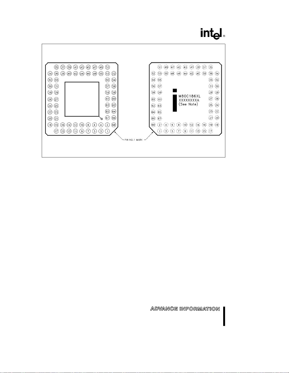
M80C186XL
Pins Facing Up Pins Facing Down
NOTE:
XXXXXXXXA indicates the Intel FPO number.
Figure 2. M80C186XL Pinout Diagrams
Ceramic Pin Grid Array
271276– 3
4
Page 5
M80C186XL
Table 1. M80C186XL Pin Description
Symbol
V
CC
V
SS
RESET 57 O RESET Output indicates that the M80C186XL CPU is being reset, and
X1 59 I Crystal Inputs X1 and X2 provide external connections for a
X2 58 O
CLKOUT 56 O Clock Output provides the system with a 50% duty cycle waveform.
RES 24 I An active RES causes the M80C186XL to immediately terminate its
TEST/BUSY 47 I/O The TEST pin is sampled during and after reset to determine whether
PGA
Pin No.
Type Name and Function
9 I System Power:a5 volt power supply.
43 I
26 I System Ground.
60 I
can be used as a system reset. It is active HIGH, synchronized with
the processor clock, and lasts an integer number of clock periods
corresponding to the length of the RES
clockout periods after RES
goes inactive. When tied to the TEST/
BUSY pin, RESET forces the M80C186XL into enhanced mode.
RESET is not floated during bus hold.
fundamental mode or third overtone parallel resonant crystal for the
internal oscillator. X1 can connect to an external clock instead of a
crystal. In this case, minimize the capacitance on X2. The input or
oscillator frequency is internally divided by two to generate the clock
signal (CLKOUT).
All device pin timings are specified relative to CLKOUT. CLKOUT is
active during reset and bus hold.
present activity, clear the internal logic, and enter a dormant state.
This signal may be asynchronous to the M80C186XL clock. The
M80C186XL begins fetching instructions approximately 6(/2 clock
cycles after RES
is returned HIGH. For proper initialization, VCCmust
be within specifications and the clock signal must be stable for more
than 4 clocks with RES
held LOW. RES is internally synchronized.
This input is provided with a Schmitt-trigger to facilitate power-on RES
generation via an RC network.
the M80C186XL is to enter Compatible or Enhanced Mode. Enhanced
Mode requires TEST
to be HIGH on the rising edge of RES and LOW
four CLKOUT cycles later. Any other combination will place the
M80C186XL in Compatible Mode. During power-up, active RES is
required to configure TEST
/BUSY as an input. A weak internal pullup
ensures a HIGH state when the input is not externally driven.
ÐIn Compatible Mode this pin is configured to operate as TEST.
TEST
This pin is examined by the WAIT instruction. If the TEST
HIGH when WAIT execution begins, instruction execution will
suspend. TEST
will be resampled every five clocks until it goes LOW,
at which time execution will resume. If interrupts are enabled while the
M80C186XL is waiting for TEST
BUSYÐIn Enhanced Mode, this pin is configured to operate as
BUSY. The BUSY input is used to notify the M80C186XL of Math
Coprocessor activity. Floating point instructions executing in the
M80C186XL sample the BUSY pin to determine when the Math
Coprocessor is ready to accept a new command. BUSY is active
HIGH.
signal. Reset goes inactive 2
input is
, interrupts will be serviced.
5
Page 6
M80C186XL
Table 1. M80C186XL Pin Description (Continued)
Symbol
TMR IN 0 20 I Timer Inputs are used either as clock or control signals,
TMR IN 1 21 I
TMR OUT 0 22 O Timer outputs are used to provide single pulse or continous
TMR OUT 1 23 O
DRQ0 18 I DMA Request is asserted HIGH by an external device when it is
DRQ1 19 I
NMI 46 I The Non-Maskable Interrupt input causes a Type 2 interrupt. An
INT0 45 I Maskable Interrupt Requests can be requested by activating one
INT1/SELECT
INT2/INTA0
INT3/INTA1
/IRQ 41 I/O
A19/S6 65 O Address Bus Outputs (16 –19) and Bus Cycle Status (3 –6)
A18/S5 66 O
A17/S4 67 O
A16/S3 68 O During T
AD15 1 I/O Address/Data Bus (0 –15) signals constitute the time multiplexed
AD14 3 I/O
AD13 5 I/O
AD12 7 I/O
AD11 10 I/O
AD10 12 I/O
AD9 14 I/O
AD8 16 I/O
AD7 2 I/O
AD6 4 I/O
AD5 6 I/O
AD4 8 I/O
AD3 11 I/O
AD2 13 I/O
AD1 15 I/O
AD0 17 I/O
PGA
Pin No.
44 I
42 I/O
Type Name and Function
depending upon the programmed timer mode. These inputs are
active HIGH (or LOW-to-HIGH transitions are counted) and
internally synchronized. Timer Inputs must be tied HIGH when
not being used as clock or retrigger inputs.
waveform generation, depending upon the timer mode selected.
These outputs are not floated during a bus hold.
ready for DMA Channel 0 or 1 to perform a transfer. These
signals are level-triggered and internally synchronized.
NMI transition from LOW to HIGH is latched and synchronized
internally, and initiates the interrupt at the next instruction
boundary. NMI must be asserted for at least one CLKOUT period.
The Non-Maskable Interrupt cannot be avoided by programming.
of these pins. When configured as inputs, these pins are active
HIGH. Interrupt Requests are synchronized internally. INT2 and
INT3 may be configured to provide active-LOW interruptacknowledge output signals. All interrupt inputs may be
configured to be either edge- or level-triggered. To ensure
recognition, all interrupt requests must remain active until the
interrupt is acknowledged. When Slave Mode is selected, the
function of these pins changes (see Interrupt Controller section
of this data sheet).
indicate the four most significant address bits during T
signals are active HIGH.
2,T3,TW
initiated bus cycle or HIGH to indicate a DMA-initiated or refresh
and T4, the S6 pin is LOW to indicate a CPU-
bus cycle. During the same T-states, S3, S4 and S5 are always
LOW. These outputs are floated during bus hold or reset.
memory or I/O address (T
The bus is active HIGH. A
byte of the data bus, pins D
when a byte is to be transferred onto the lower portion of the bus
) and data (T2,T3,TWand T4) bus.
1
is analogous to BHE for the lower
0
through D0. It is LOW during T
7
in memory or I/O operations. These pins are floated during a bus
hold or reset.
. These
1
1
6
Page 7
M80C186XL
Table 1. M80C186XL Pin Description (Continued)
Symbol
BHE 64 O The BHE (Bus High Enable) signal is analogous to A0 in that it is used
ALE/QS0 61 O Address Latch Enable/Queue Status 0 is provided by the M80C186XL
WR/QS1 63 O Write Strobe/Queue Status 1 indicates that the data on the bus is to be
RD/QSMD 62 O/I Read Strobe is an active LOW signal which indicates that the
ARDY 55 I Asynchronous Ready informs the M80C186XL that the addressed
SRDY 49 I Synchronous Ready informs the M80C186XL that the addressed
PGA
Pin No.
Type Name and Function
to enable data on to the most significant half of the data bus, pins D15–
D8. BHE
will remain LOW through T
BHE
will be LOW during T1when the upper byte is transferred and
AND TW. BHE does not need to be latched.
will float during HOLD or RESET.
3
In Enhanced Mode, BHE will also be used to signify DRAM refresh
cycles. A refresh cycle is indicated by both BHE
BHE and A0 Encodings
BHE A0
Value Value
Function
0 0 Word Transfer
0 1 Byte Transfer on upper half of data bus (D15–D8)
1 0 Byte Transfer on lower half of data bus (D
1 1 Refresh
to latch the address. ALE is active HIGH, with addresses guaranteed
valid on the trailing edge.
written into a memory or an I/O device. It is active LOW, and floats
during bus hold or reset. When the M80C186XL is in Queue Status
Mode, the ALE/QS0 and WR
/QS1 pins provide information about
processor/instruction queue interaction.
QS1 QS0 Queue Operation
0 0 No queue operation
0 1 First opcode byte fetched from the queue
1 1 Subsequent byte fetched from the queue
1 0 Empty the queue
M80C186XL is performing a memory or I/O read cycle. It is guaranteed
not to go LOW before the A/D bus is floated. An internal pull-up
ensures that RD
/QSMD is HIGH during RESET. Following RESET the
pin is sampled to determine whether the M80C186XL is to provide ALE,
RD
, and WR, or queue status information. To enable Queue Status
Mode, RD
must be connected to GND. RD will float during bus HOLD.
memory space or I/O device will complete a data transfer. The ARDY
pin accepts a rising edge that is asynchronous to CLKOUT and is active
HIGH. The falling edge of ARDY must be synchronized to the
M80C186XL clock. Connecting ARDY HIGH will always assert the
ready condition to the CPU. If this line is unused, it should be tied LOW
to yield control to the SRDY pin.
memory space or I/O device will complete a data transfer. The SRDY
pin accepts an active-HIGH input synchronized to CLKOUT. The use of
SRDY allows a relaxed system timing over ARDY. This is accomplished
by elimination of the one-half clock cycle required to internally
synchonize the ARDY input signal. Connecting SRDY high will always
assert the ready condition to the CPU. If this line is unused, it should be
tied LOW to yield control to the ARDY pin.
and A0 being HIGH.
7–D0
)
7
Page 8
M80C186XL
Table 1. M80C186XL Pin Description (Continued)
Symbol
LOCK 48 O LOCK output indicates that other system bus masters are not to gain
S0 52 O Bus cycle status S0 –S2
S1
S2 54 O
HOLD 50 I HOLD indicates that another bus master is requesting the local bus. The
HLDA 51 O
UCS 34 O/I Upper Memory Chip Select is an active LOW output whenever a memory
LCS 33 O/I Lower Memory Chip Select is active LOW whenever a memory reference is
PGA
Pin No.
53 O
Type Name and Function
control of the system bus. LOCK
requested by the LOCK prefix instruction and is activated at the beginning
of the first data cycle associated with the instruction immediately following
the LOCK prefix. It remains active until the completion of that instruction.
No instruction prefetching will occur while LOCK is asserted. LOCK floats
during bus hold or reset.
information:
M80C186XL Bus Cycle Status Information
S2 S1 S0 Bus Cycle Initiated
0 0 0 Interrupt Acknowledge
0 0 1 Read I/O
0 1 0 Write I/O
0 1 1 Halt
1 0 0 Instruction Fetch
1 0 1 Read Data from Memory
1 1 0 Write Data to Memory
1 1 1 Passive (no bus cycle)
The status pins float during HOLD.
S2
may be used as a logical M/IO indicator, and S1 as a DT/R indicator.
HOLD input is active HIGH. The M80C186XL generates HLDA (HIGH) in
response to a HOLD request. Simultaneous with the issuance of HLDA,
the M80C186XL will float the local bus and control lines. After HOLD is
detected as being LOW, the M80C186XL will lower HLDA. When the
M80C186XL needs to run another bus cycle, it will again drive the local bus
and control lines.
In Enhanced Mode, HLDA will go low when a DRAM refresh cycle is
pending in the M80C186XL and an external bus master has control of the
bus. It will be up to the external master to relinquish the bus by lowering
HOLD so that the M80C186XL may execute the refresh cycle.
reference is made to the defined upper portion (1K – 256K block) of
memory. UCS
is software programmable.
UCS
UCS and LCS are sampled upon the rising edge of RES. If both pins are
held low, the M80C186XL will enter ONCE Mode. In ONCE Mode all pins
assume a high impedance state and remain so until a subsequent RESET.
UCS has a weak internal pullup that is active during RESET to ensure that
the M80C186XL does not enter ONCE Mode inadvertently.
made to the defined lower portion (1K –256K) of memory. LCS
float during bus HOLD. The address range activating LCS
programmable.
does not float during bus hold. The address range activating
is active LOW. The LOCK signal is
are encoded to provide bus-transaction
does not
is software
8
Page 9
M80C186XL
Table 1. M80C186XL Pin Description (Continued)
Symbol
LCS UCS and LCS are sampled upon the rising edge of RES. If both
(Continued)
MCS0/PEREQ 38 O/I Mid-Range Memory Chip Select signals are active LOW when a
MCS1
/ERROR 37 O/I
MCS2
MCS3
/NPS 35 O
PCS0 25 O Peripheral Chip Select signals 0–4 are active LOW when a
PCS1
PCS2
PCS3
PCS4
PCS5/A1 31 O Peripheral Chip Select 5 or Latched A1 may be programmed to
PCS6/A2 32 O Peripheral Chip Select 6 or Latched A2 may be programmed to
DT/R 40 O Data Transmit/Receive controls the direction of data flow through
DEN 39 O Data Enable is provided as a data bus transceiver output enable.
N.C. Ð Ð Not connected. To maintain compatibility with future products, do
PGA
Pin No.
36 O
27 O
28 O
29 O
30 O
Type Name and Function
pins are held low, the M80C186XL will enter ONCE Mode. In ONCE
Mode all pins assume a high impedance state and remain so until a
subsequent RESET. LCS
only during RESET to ensure that the M80C186XL does not enter
ONCE mode inadvertently.
memory reference is made to the defined mid-range portion of
memory (8K –512K). These lines do not float during bus HOLD. The
address ranges activating MCS0 – 3
In Enhanced Mode, MCS0
Extension Request). When connected to the Math Coprocessor,
this input is used to signal the M80C186XL when to make numeric
data transfers to and from the coprocessor. MCS3
(Numeric Processor Select) which may only be activated by
communication to the 80C187. MCS1
Enhanced Mode and is used to signal numerics coprocessor errors.
MCS0
/PEREQ and MCS1/ERROR have weak internal pullups
which are active during reset.
reference is made to the defined peripheral area (64K byte I/O or 1
MByte memory space). These lines do not float during bus HOLD.
The address ranges activating PCS0–4
programmable.
provide a sixth peripheral chip select, or to provide an internally
latched A1 signal. The address range activating PCS5 is softwareprogrammable. PCS5
programmed to provide latched A1, this pin will retain the previously
latched value during HOLD.
provide a seventh peripheral chip select, or to provide an internally
latched A2 signal. The address range activating PCS6
programmable. PCS6/A2 does not float during bus HOLD. When
programmed to provide latched A2, this pin will retain the previously
latched value during HOLD.
an external data bus transceiver. When LOW, data is transferred to
the M80C186XL. When HIGH the M80C186XL places write data on
the data bus. DT/R
DEN
is active LOW during each memory and I/O access (including
80C187 access). DEN
During RESET, DEN
DEN
also floats during HOLD.
not connect to these pins.
has a weak internal pullup that is active
are software programmable.
becomes a PEREQ input (Processor
becomes ERROR in
are software
/A1 does not float during bus HOLD. When
floats during a bus hold or reset.
is HIGH whenever DT/R changes state.
is driven HIGH for one clock, then floated.
becomes NPS
is software-
9
Page 10
M80C186XL
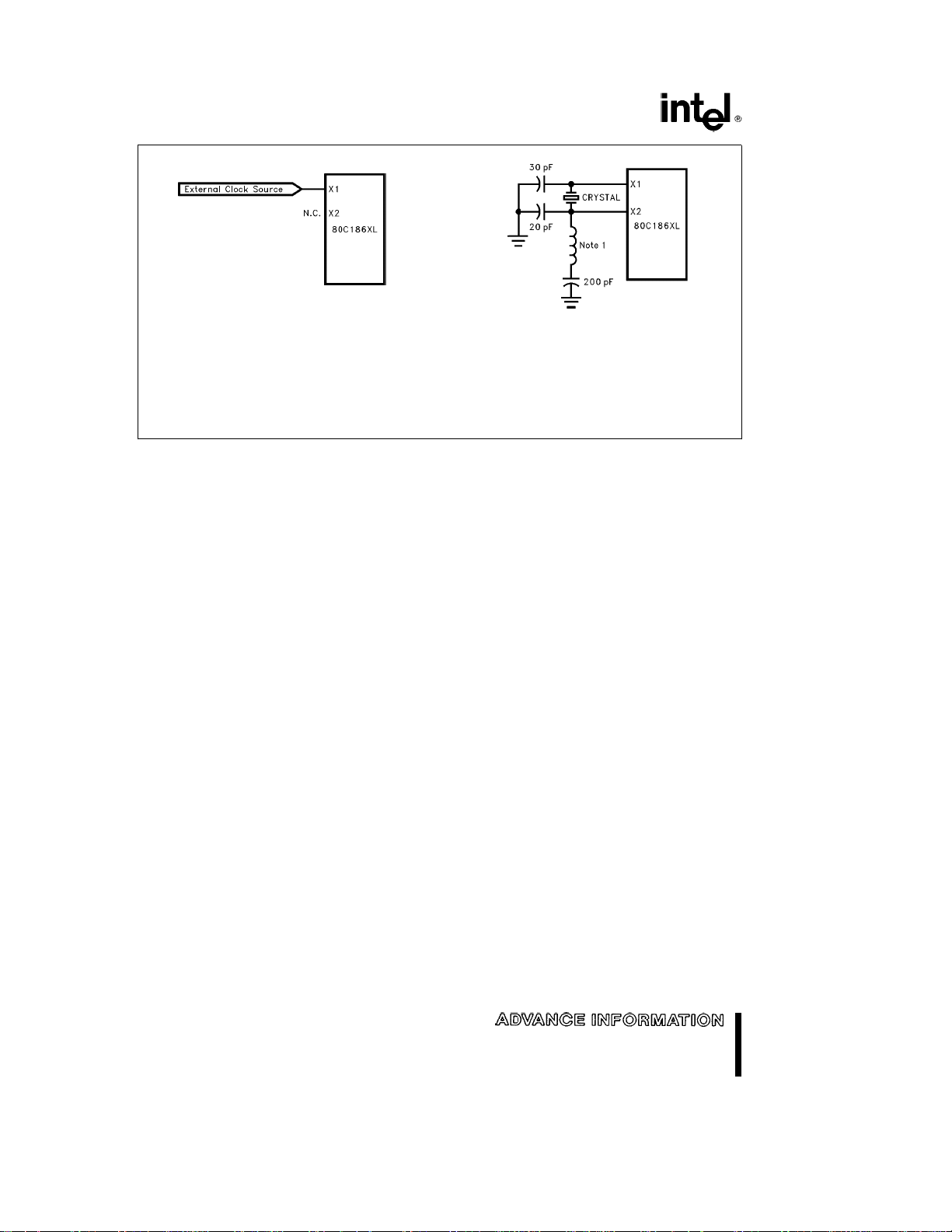
(3a)
271276– 4
Figure 3. M80C186XL Oscillator Configurations (see text)
INTRODUCTION
The following Functional Description describes the
base architecture of the M80C186XL. The
M80C186XL is a very high integration 16-bit microprocessor. It combines 15 –20 of the most common
microprocessor system components onto one chip.
The M80C186XL is object code compatible with the
8086/8088 microprocessors and adds 10 new instruction types to the 8086/8088 instruction set.
The M80C186XL has two major modes of operation,
Compatible and Enhanced. In Compatible Mode the
M80C186XL is completely compatible with NMOS
80186, with the exception of 8087 support. The Enhanced mode adds three new features to the system
design. These are Power-Save control, Dynamic
RAM refresh, and an asynchronous Numerics Coprocessor interface.
271276– 5
(3b)
Note 1:
XTAL Frequency L1 Value
20 MHz 12.0 mH
25 MHz 8.2 mH
32 MHz 4.7 mH
40 MHz 3.0 mH
LC network is only required when using a third
overtone crystal.
g
20%
g
20%
g
20%
g
20%
third-overtone mode crystal, depending upon the
frequency range of the application. This is used as
the time base for the M80C186XL.
The output of the oscillator is not directly available
outside the M80C186XL. The recommended crystal
configuration is shown in Figure 3b. When used in
third-overtone mode, the tank circuit is recommended for stable operation. Alternately, the oscillator
may be driven from an external source as shown in
Figure 3a.
The crystal or clock frequency chosen must be twice
the required processor operating frequency due to
the internal divide by two counter. This counter is
used to drive all internal phase clocks and the external CLKOUT signal. CLKOUT is a 50% duty cycle
processor clock and can be used to drive other system components. All AC Timings are referenced to
CLKOUT.
M80C186XL BASE ARCHITECTURE
M80C186XL Clock Generator
The M80C186XL provides an on-chip clock generator for both internal and external clock generation.
The clock generator features a crystal oscillator, a
divide-by-two counter, synchronous and asynchronous ready inputs, and reset circuitry.
The M80C186XL oscillator circuit is designed to be
used either with a parallel resonant fundamental or
10
Intel recommends the following values for crystal selection parameters.
Temperature Range: Application Specific
ESR (Equivalent Series Resistance): 60X max
C
(Shunt Capacitance of Crystal): 7.0 pF max
0
C1(Load Capacitance): 20 pFg5pF
Drive Level: 2 mW max
Page 11
M80C186XL
Bus Interface Unit
The M80C186XL provides a local bus controller to
generate the local bus control signals. In addition, it
employs a HOLD/HLDA protocol for relinquishing
the local bus to other bus masters. It also provides
outputs that can be used to enable external buffers
and to direct the flow of data on and off the local
bus.
The bus controller is responsible for generating 20
bits of address, read and write strobes, bus cycle
status information and data (for write operations) information. It is also responsible for reading data
from the local bus during a read operation. Synchronous and asynchronous ready input pins are provided to extend a bus cycle beyond the minimum four
states (clocks).
The M80C186XL bus controller also generates two
control signals (DEN
external transceiver chips. This capability allows the
addition of transceivers for simple buffering of the
multiplexed address/data bus.
During RESET the local bus controller will perform
the following action:
Drive DEN
#
cle, then float them.
Drive S0–S2 to the inactive state (all HIGH) and
#
then float.
Drive LOCK HIGH and then float.
#
Float AD0–15, A16 – 19, BHE, DT/R.
#
Drive ALE LOW
#
Drive HLDA LOW.
#
RD
/QSMD, UCS, LCS, MCS0/PEREQ, MCS1/
ERROR
and TEST/BUSY pins have internal pullup
devices which are active while RES
cessive loading or grounding certain of these pins
causes the M80C186XL to enter an alternative
mode of operation:
RD/QSMD low results in Queue Status Mode.
#
UCS and LCS low results in ONCE Mode.
#
TEST/BUSY low (and high later) results in En-
#
hanced Mode.
and DT/R) when interfacing to
,RDand WR HIGH for one clock cy-
is applied. Ex-
Chip-Select/Ready Generation Logic
The M80C186XL contains logic which provides programmable chip-select generation for both memories and peripherals. In addition, it can be programmed to provide READY (or WAIT state) generation. It can also provide latched address bits A1 and
A2. The chip-select lines are active for all memory
and I/O cycles in their programmed areas, whether
they be generated by the CPU or by the integrated
DMA unit.
The M80C186XL provides 6 memory chip select outputs for 3 address areas; upper memory, lower
memory, and midrange memory. One each is provided for upper memory and lower memory, while four
are provided for midrange memory.
OFFSET
Relocation Register FEH
DMA Descriptors Channel 1
DMA Descriptors Channel 0
Chip-Select Control Registers
Time 2 Control Registers
Time 1 Control Registers
Time 0 Control Registers
Interrupt Controller Registers
DAH
D0H
CAH
C0H
A8H
A0H
66H
60H
5EH
58H
56H
50H
3EH
20H
M80C186XL PERIPHERAL
ARCHITECTURE
All the M80C186XL integrated peripherals are controlled by 16-bit registers contained within an internal 256-byte control block. The control block may be
mapped into either memory or I/O space. Internal
logic will recognize control block addresses and respond to bus cycles. An offset map of the 256-byte
control register block is shown in Figure 4.
Figure 4. Internal Register Map
The M80C186XL provides a chip select, called UCS
for the top of memory. The top of memory is usually
used as the system memory because after reset the
M80C186XL begins executing at memory location
FFFF0H.
11
,
Page 12

M80C186XL
The M80C186XL provides a chip select for low
memory called LCS
tains the interrupt vector table, starting at location
00000H.
The M80C186XL provides four MCS lines which are
active within a user-locatable memory block. This
block can be located within the M80C186XL 1 Mbyte
memory address space exclusive of the areas defined by UCS
size of this memory block are programmable.
The M80C186XL can generate chip selects for up to
seven peripheral devices. These chip selects are active for seven contiguous blocks of 128 bytes above
a programmable base address. The base address
may be located in either memory or I/O space.
The M80C186XL can generate a READY signal internally for each of the memory or peripheral CS
lines. The number of WAIT states to be inserted for
each peripheral or memory is programmable to provide 0–3 wait states for all accesses to the area for
which the chip select is active. In addition, the
M80C186XL may be programmed to either ignore
external READY for each chip-select range individually or to factor external READY with the integrated
ready generator.
Upon RESET, the Chip-Select/Ready Logic will perform the following actions:
All chip-select outputs will be driven HIGH.
#
Upon leaving RESET, the UCS line will be pro-
#
grammed to provide chip selects to a 1K block
with the accompanying READY control bits set at
011 to insert 3 wait states in conjunction with external READY (i.e., UMCS resets to FFFBH).
No other chip select or READY control registers
#
have any predefined values after RESET. They
will not become active until the CPU accesses
their control registers.
. The bottom of memory con-
and LCS. Both the base address and
DMA Unit
The M80C186XL DMA controller provides two independent high-speed DMA channels. Data transfers
can occur between memory and I/O spaces (e.g.,
Memory to I/O) or within the same space (e.g.,
Memory to Memory or I/O to I/O). Data can be
transferred either in bytes (8 bits) or in words (16
bits) to or from even or odd addresses. Each DMA
channel maintains both a 20-bit source and destination pointer which can be optionally incremented or
decremented after each data transfer (by one or two
depending on byte or word transfers). Each data
transfer consumes 2 bus cycles (a minimum of 8
clocks), one cycle to fetch data and the other to
store data.
Timer/Counter Unit
The M80C186XL provides three internal 16-bit programmable timers. Two of these are highly flexible
and are connected to four external pins (2 per timer).
They can be used to count external events, time external events, generate nonrepetitive waveforms,
etc. The third timer is not connected to any external
pins, and is useful for real-time coding and time delay applications. In addition, the third timer can be
used as a prescaler to the other two, or as a DMA
request source.
Interrupt Control Unit
The M80C186XL can receive interrupts from a number of sources, both internal and external. The
M80C186XL has 5 external and 2 internal interrupt
sources (Timer/Couners and DMA). The internal interrupt controller serves to merge these requests on
a priority basis, for individual service by the CPU.
Enhanced Mode Operation
In Compatible Mode the M80C186XL operates with
all the features of the NMOS 80186, with the exception of 8087 support (i.e. no math coprocessing is
possible in Compatible Mode). Queue-Status information is still available for design purposes other
than 8087 support.
All the Enhanced Mode features are completely
masked when in Compatible Mode. A write to any of
the Enhanced Mode registers will have no effect,
while a read will not return any valid data.
In Enhanced Mode, the M80C186XL will operate
with Power-Save, DRAM refresh, and numerics coprocessor support in addition to all the Compatible
Mode features.
If connected to a math coprocessor, this mode will
be invoked automatically. Without an NPX, this
mode can be entered by tying the RESET output
signal from the M80C186XL to the TEST
put.
/BUSY in-
Queue-Status Mode
The queue-status mode is entered by strapping the
RD
pin low. RD is sampled at RESET and if LOW,
the M80C186XL will reconfigure the ALE and WR
pins to be QS0 and QS1 respectively. This mode is
available on the M80C186XL in both Compatible
and Enhanced Modes.
12
Page 13
M80C186XL
DRAM Refresh Control Unit
The Refresh Control Unit (RCU) automatically generates DRAM refresh bus cycles. The RCU operates
only in Enhanced Mode. After a programmable period of time, the RCU generates a memory read request to the BIU. If the address generated during a
refresh bus cycle is within the range of a properly
programmed chip select, that chip select will be activated when the BIU executes the refresh bus cycle.
Power-Save Control
The M80C186XL, when in Enhanced Mode, can enter a power saving state by internally dividing the
processor clock frequency by a programmable factor. This divided frequency is also available at the
CLKOUT pin.
All internal logic, including the Refresh Control Unit
and the timers, have their clocks slowed down by
the division factor. To maintain a real time count or a
fixed DRAM refresh rate, these peripherals must be
re-programmed when entering and leaving the power-save mode.
Interface for 80C187 Math
Coprocessor
In Enhanced Mode, three of the mid-range memory
chip selects are redefined according to Table 2 for
use with the 80C187. The fourth chip select, MCS2
functions as in compatible mode, and may be pro-
grammed for activity with ready logic and wait states
accordingly. As in Compatible Mode, MCS2
tion for one-fourth a programmed block size.
Table 2. MCS
Compatible
Mode
MCS0 PEREQ Processor Extension Request
MCS1
MCS2
MCS3
ERROR NPX Error
MCS2 Mid-Range Chip Select
NPS Numeric Processor Select
Assignments
Enhanced Mode
will func-
ONCE Test Mode
To facilitate testing and inspection of devices when
fixed into a target system, the M80C186XL has a
test mode available which allows all pins to be
placed in a high-impedance state. ONCE stands for
‘‘ON Circuit Emulation’’. When placed in this mode,
the M80C186XL will put all pins in the high-impedance state until RESET.
The ONCE mode is selected by tying the UCS
the LCS
pled on the low-to-high transition of the RES
The UCS
up resistors similar to the RD
to guarantee ONCE Mode is not entered inadvertently during normal operation. LCS
be held low at least one clock after RES
to guarantee entrance into ONCE Mode.
LOW during RESET. These pins are sam-
and the LCS pins have weak internal pull-
and TEST/BUSY pins
and UCS must
and
pin.
goes high
13
Page 14
M80C186XL
ABSOLUTE MAXIMUM RATINGS*
Case Temperature under Bias ÀÀÀb55§Ctoa125§C
Storage Temperature ААААААААААb65§Ctoa150§C
Voltage on Any Pin with
Respect to Ground АААААААААААА
/Package Power Dissipation АААААААААААААААААА1W
Not to exceed the maximum allowable die temperature based on thermal resistance of the package.
b
1.0V toa7.0V
NOTICE: This data sheet contains information on
products in the sampling and initial production phases
of development. It is valid for the devices indicated in
the revision history. The specifications are subject to
change without notice.
*
WARNING: Stressing the device beyond the ‘‘Absolute
Maximum Ratings’’ may cause permanent damage.
These are stress ratings only. Operation beyond the
‘‘Operating Conditions’’ is not recommended and extended exposure beyond the ‘‘Operating Conditions’’
may affect device reliability.
NOTICE: The specifications are subject to change
without notice.
DC CHARACTERISTICS T
eb
55§Ctoa125§C, V
C
CC
e
5Vg10%
Symbol Parameter Min Max Units Test Conditions
V
V
V
V
V
V
V
I
Input Low Voltage (Except X1)
IL
Clock Input Low Voltage (X1)
IL1
Input High Voltage 0.2 V
IH
(All except X1 and RES
Input High Voltage (RES) 3.0 V
IH1
Clock Input High Voltage (X1) 3.9 V
IH2
Output Low Voltage 0.45 V I
OL
Output High Voltage 2.4 V
OH
Power Supply Current 100 mA@20 MHz,b55§C
CC
)
b
0.5 0.2 V
b
0.5 0.6 V
a
0.9 V
CC
b
V
0.5 V
CC
CC
CC
CC
CC
a
a
a
CC
CC
b
0.3 V
0.5 V
0.5 V
0.5 V
OL
I
OL
VI
OH
VI
OH
V
CC
e
2.5 mA (S0, 1, 2)
e
2.0 mA (others)
eb
2.4 mA@2.4V
eb
200 mA@V
(3)
e
5.5V
CC
90 mA@16 MHz,b55§C
(3)
e
V
5.5V
CC
80 mA@12.5 MHz,b55§C
(3)
e
5.5V
V
CC
70 mA@10 MHz,b55§C
(3)
e
V
5.5V
CC
I
I
V
Input Leakage Current
LI
Output Leakage Current
LO
Clock Output Low 0.45 V I
CLO
g
10 mA@0.5 MHz,
0.45V
g
10 mA@0.5 MHz,
0.45VsV
CLO
s
e
V
IN
OUT
4.0 mA
s
V
CC
s
V
CC
(1)
(4)
b
0.5
(4)
14
Page 15

M80C186XL
DC CHARACTERISTICS (Continued) T
eb
55§Ctoa125§C, V
C
CC
e
5Vg10%
Symbol Parameter Min Max Units Test Conditions
V
CHO
C
IN
C
IO
NOTES:
1. Pins being floated during HOLD or by invoking the ONCE Mode.
2. Characterization conditions are a) Frequency
parameter is not tested.
3. Current is measured with the device in RESET with X1 and X2 driven and all other non-power pins open.
/QSMD, UCS, LCS, MCS0/PEREQ, MCS1/ERROR and TEST/BUSY pins have internal pullup devices. Loading some
4. RD
of these pins above I
on Local Bus Controller and Reset for details.
Clock Output High V
Input Capacitance 10 pF
Output or I/O Capacitance 20 pF
e
eb
200 mA can cause the M80C186XL to go into alternative modes of operation. See the section
OH
b
0.5 V I
CC
1 MHz; b) Unmeasured pins at GND; c) VINata5.0V or 0.45V. This
CHO
@
@
eb
1 MHz
1 MHz
(2)
(2)
500 mA
15
Page 16

M80C186XL
AC CHARACTERISTICS
MAJOR CYCLE TIMINGS (READ CYCLE)
eb
T
All timings are measured at 1.5V and 100 pF loading on CLKOUT unless otherwise noted.
55§Ctoa125§C, V
C
All output test conditions are with C
For AC tests, input V
IL
Symbol Parameter M80C186XL M80C186XL12 Unit
M80C186XL GENERAL TIMING REQUIREMENTS (Listed More Than Once)
T
DVCL
T
CLDX
Data in Setup (A/D) 15 15 ns
Data in Hold (A/D) 3 3 ns
M80C186XL GENERAL TIMING RESPONSES (Listed More Than Once)
T
CHSV
T
CLSH
T
CLAV
T
CLAX
T
CLDV
T
CHDX
T
CHLH
T
LHLL
T
CHLL
T
AVLL
T
LLAX
T
AVCH
T
CLAZ
T
CLCSV
T
CXCSX
T
CHCSX
T
DXDL
T
CVCTV
T
CVDEX
T
CHCTV
T
CLLV
Status Active Delay 3 45 3 35 ns
Status Inactive Delay 3 46 3 35 ns
Address Valid Delay 3 44 3 36 ns
Address Hold 0 0 ns
Data Valid Delay 3 40 3 36 ns
Status Hold Time 10 10 ns
ALE Active Delay 30 25 ns
ALE Width T
ALE Inactive Delay 30 25 ns
Address Valid to ALE Low T
Address Hold from ALE T
Inactive Loading
Address Valid to Clock High 0 0 ns
Address Float Delay T
Chip-Select Active Delay 3 42 3 33 ns
Chip-Select Hold from T
Command Inactive Loading
Chip-Select Inactive Delay 3 35 3 30 ns
DEN Inactive to DT/R Low 0 0 ns Equal
Control Active Delay 1 3 44 3 37 ns
DEN Inactive Delay 3 44 3 37 ns
Control Active Delay 2 3 44 3 37 ns
LOCK Valid/Invalid Delay 3 40 3 37 ns
M80C186XL TIMING RESPONSES (Read Cycle)
T
AZRL
T
CLRL
T
RLRH
T
CLRH
T
RHLH
T
RHAV
Address Float to RD Active 0 0 ns
RD Active Delay 3 44 3 37 ns
RD Pulse Width 2T
RD Inactive Delay 3 44 3 37 ns
RD Inactive to ALE High T
RD Inactive to Address T
Active Loading
CC
e
0.45V and V
e
5Vg10%
L
e
50 pF.
e
2.4V except at X1 where V
IH
Min Max Min Max
b
15 T
CLCL
b
CLAX
CLCL
b
b
b
b
b
18 T
15 T
10 T
30 2T
14 T
15 T
CLCH
CHCL
CLCH
CLCH
CLCL
Values
CLCL
CLCH
CHCL
30 T
CLCH
CLCL
CLCH
CLCL
e
b
V
CC
0.5V.
25 ns
IH
b
15 ns
b
15 ns Equal
b
15 ns Equal
CLAX
b
10 ns Equal
b
25 ns
b
14 ns Equal
b
15 ns Equal
Test
Conditions
Loading
Loading
Loading
16
Page 17

AC CHARACTERISTICS
MAJOR CYCLE TIMINGS (READ CYCLE)
eb
T
All timings are measured at 1.5V and 100 pF loading on CLKOUT unless otherwise noted.
55§Ctoa125§C, V
C
All output test conditions are with C
For AC tests, input V
IL
Symbol Parameter M80C186XL16 M80C186XL20 Unit
M80C186XL GENERAL TIMING REQUIREMENTS (Listed More Than Once)
T
DVCL
T
CLDX
Data in Setup (A/D) 15 10 ns
Data in Hold (A/D) 3 3 ns
M80C186XL GENERAL TIMING RESPONSES (Listed More Than Once)
T
CHSV
T
CLSH
T
CLAV
T
CLAX
T
CLDV
T
CHDX
T
CHLH
T
LHLL
T
CHLL
T
AVLL
T
LLAX
T
AVCH
T
CLAZ
T
CLCSV
T
CXCSX
T
CHCSX
T
DXDL
T
CVCTV
T
CVDEX
T
CHCTV
T
CLLV
Status Active Delay 1 31 1 25 ns
Status Inactive Delay 1 30 1 25 ns
Address Valid Delay 1 33 1 27 ns
Address Hold 0 0 ns
Data Valid Delay 1 33 1 27 ns
Status Hold Time 10 10 ns
ALE Active Delay 20 20 ns
ALE Width T
ALE Inactive Delay 20 20 ns
Address Valid to ALE Low T
Address Hold from ALE T
Inactive Loading
Address Valid to Clock High 0 0 ns
Address Float Delay T
Chip-Select Active Delay 1 30 1 25 ns
Chip-Select Hold from t
Command Inactive Loading
Chip-Select Inactive Delay 1 25 1 20 ns
DEN Inactive to DT/R Low 0 0 ns Equal
Control Active Delay 1 1 31 1 22 ns
DEN Inactive Delay 1 31 1 22 ns
Control Active Delay 2 1 31 1 22 ns
LOCK Valid/Invalid Delay 1 35 1 22 ns
M80C186XL TIMING RESPONSES (Read Cycle)
T
AZRL
T
CLRL
T
RLRH
T
CLRH
T
RHLH
T
RHAV
Address Float to RD Active 0 0 ns
RD Active Delay 1 31 1 27 ns
RD Pulse Width 2T
RD Inactive Delay 1 31 1 27 ns
RD Inactive to ALE High T
RD Inactive to Address T
Active Loading
CC
e
0.45V and V
e
5Vg10%
L
e
50 pF.
e
2.4V except at X1 where V
IH
Min Max Min Max
b
15 T
CLCL
b
CLAX
CLCL
b
b
b
b
b
15 T
15 T
10 T
25 2T
14 T
15 T
CLCH
CHCL
CLCH
CLCH
CLCL
Values
CLCL
CLCH
CHCL
20 T
CLCH
CLCL
CLCH
CLCL
e
b
V
CC
0.5V.
20 ns
IH
b
15 ns
b
10 ns Equal
b
10 ns Equal
CLAX
b
10 ns Equal
b
20 ns
b
14 ns Equal
b
15 ns Equal
M80C186XL
Test
Conditions
Loading
Loading
Loading
17
Page 18

M80C186XL
AC CHARACTERISTICS
MAJOR CYCLE TIMINGS (WRITE CYCLE)
eb
T
All timings are measured at 1.5V and 100 pF loading on CLKOUT unless otherwise noted.
55§Ctoa125§C, V
C
All output test conditions are with C
For AC tests, input V
IL
Symbol Parameter M80C186XL M80C186XL12 Unit
M80C186XL GENERAL TIMING RESPONSES (Listed More Than Once)
T
CHSV
T
CLSH
T
CLAV
T
CLAX
T
CLDV
T
CHDX
T
CHLH
T
LHLL
T
CHLL
T
AVLL
T
LLAX
Status Active Delay 3 45 3 35 ns
Status Inactive Delay 3 46 3 35 ns
Address Valid Delay 3 44 3 36 ns
Address Hold 0 0 ns
Data Valid Delay 3 40 3 36 ns
Status Hold Time 10 10 ns
ALE Active Delay 30 25 ns
ALE Width T
ALE Inactive Delay 30 25 ns
Address Valid to ALE Low T
Address Hold from ALE T
Inactive Loading
T
AVCH
T
CLDOX
T
CVCTV
T
CVCTX
T
CLCSV
T
CXCSX
Address Valid to Clock High 0 0 ns
Data Hold Time 3 3 ns
Control Active Delay 1 3 44 3 37 ns
Control Inactive Delay 3 44 3 37 ns
Chip-Select Active Delay 3 42 3 33 ns
Chip-Select Hold from T
Command Inactive Loading
T
CHCSX
T
DXDL
T
CLLV
Chip-Select Inactive Delay 3 35 3 30 ns
DEN Inactive to DT/R Low 0 0 ns Equal
LOCK Valid/Invalid Delay 3 40 3 37 ns
M80C186XL TIMING RESPONSES (Write Cycle)
T
WLWH
T
WHLH
T
WHDX
T
WHDEX
WR Pulse Width 2T
WR Inactive to ALE High T
Data Hold after WR T
WR Inactive to DEN Inactive T
CC
e
0.45V and V
e
5Vg10%
L
e
50 pF.
e
2.4V except at X1 where V
IH
Min Max Min Max
b
15 T
CLCL
b
CLCL
CLCL
18 T
b
15 T
b
10 T
b
30 2T
b
14 T
b
34 T
b
10 T
CLCH
CHCL
CLCH
CLCH
CLCH
Values
e
b
V
CC
0.5V.
IH
b
15 ns
CLCL
b
15 ns Equal
CLCH
b
15 ns Equal
CHCL
b
10 ns Equal
CLCH
b
25 ns
CLCL
b
14 ns Equal
CLCH
b
20 ns Equal
CLCL
b
10 ns Equal
CLCH
Test
Conditions
Loading
Loading
Loading
Loading
Loading
18
Page 19

AC CHARACTERISTICS
MAJOR CYCLE TIMINGS (WRITE CYCLE)
eb
T
All timings are measured at 1.5V and 100 pF loading on CLKOUT unless otherwise noted.
55§Ctoa125§C, V
C
All output test conditions are with C
For AC tests, input V
IL
Symbol Parameter M80C186XL16 M80C186XL20 Unit
M80C186XL GENERAL TIMING RESPONSES (Listed More Than Once)
T
CHSV
T
CLSH
T
CLAV
T
CLAX
T
CLDV
T
CHDX
T
CHLH
T
LHLL
T
CHLL
T
AVLL
T
LLAX
T
AVCH
T
CLDOX
T
CVCTV
T
CVCTX
T
CLCSV
T
CXCSX
T
CHCSX
T
DXDL
T
CLLV
Status Active Delay 1 31 1 25 ns
Status Inactive Delay 1 30 1 25 ns
Address Valid Delay 1 33 1 27 ns
Address Hold 0 0 ns
Data Valid Delay 1 33 1 27 ns
Status Hold Time 10 10 ns
ALE Active Delay 20 20 ns
ALE Width T
ALE Inactive Delay 20 20 ns
Address Valid to ALE Low T
Address Hold from ALE T
Inactive Loading
Address Valid to Clock High 0 0 ns
Data Hold Time 1 1 ns
Control Active Delay 1 1 31 1 25 ns
Control Inactive Delay 1 31 1 25 ns
Chip-Select Active Delay 1 30 1 25 ns
Chip-Select Hold from T
Command Inactive Loading
Chip-Select Inactive Delay 1 25 1 20 ns
DEN Inactive to DT/R Low 0 0 ns Equal
LOCK Valid/Invalid Delay 1 35 1 22 ns
M80C186XL TIMING RESPONSES (Write Cycle)
T
WLWH
T
WHLH
T
WHDX
T
WHDEX
WR Pulse Width 2T
WR Inactive to ALE High T
Data Hold after WR T
WR Inactive to DEN Inactive T
CC
e
0.45V and V
e
5Vg10%
L
e
50 pF.
e
2.4V except at X1 where V
IH
Min Max Min Max
b
15 T
CLCL
b
CLCL
CLCL
15 T
b
15 T
b
10 T
b
25 2T
b
14 T
b
20 T
b
10 T
CLCH
CHCL
CLCH
CLCH
CLCH
Values
e
b
V
CC
0.5V.
IH
b
15 ns
CLCL
b
10 ns Equal
CLCH
b
10 ns Equal
CHCL
b
10 ns Equal
CLCH
b
20 ns
CLCL
b
14 ns Equal
CLCH
b
15 ns Equal
CLCL
b
10 ns Equal
CLCH
M80C186XL
Test
Conditions
Loading
Loading
Loading
Loading
Loading
19
Page 20

M80C186XL
AC CHARACTERISTICS
MAJOR CYCLE TIMINGS (INTERRUPT ACKNOWLEDGE CYCLE)
eb
T
All timings are measured at 1.5V and 100 pF loading on CLKOUT unless otherwise noted.
55§Ctoa125§C, V
C
All output test conditions are with C
For AC tests, input V
IL
Symbol Parameter M80C186XL M80C186XL12 Unit
M80C186XL GENERAL TIMING REQUIREMENTS (Listed More Than Once)
T
T
DVCL
CLDX
Data in Setup (A/D) 15 15 ns
Data in Hold (A/D) 3 3 ns
M80C186XL GENERAL TIMING RESPONSES (Listed More Than Once)
T
T
T
T
T
T
T
T
T
T
T
T
CHSV
CLSH
CLAV
AVCH
CLAX
CLDV
CHDX
CHLH
LHLL
CHLL
AVLL
LLAX
Status Active Delay 3 45 3 35 ns
Status Inactive Delay 3 46 3 35 ns
Address Valid Delay 3 44 3 36 ns
Address Valid to Clock High 0 0 ns
Address Hold 0 0 ns
Data Valid Delay 3 40 3 36 ns
Status Hold Time 10 10 ns
ALE Active Delay 30 25 ns
ALE Width T
ALE Inactive Delay 30 25 ns
Address Valid to ALE Low T
Address Hold to ALE T
Inactive Loading
T
CLAZ
T
CVCTV
T
CVCTX
T
DXDL
T
CHCTV
T
CVDEX
Address Float Delay T
Control Active Delay 1 3 44 3 37 ns
Control Inactive Delay 3 44 3 37 ns
DEN Inactive to DT/R Low 0 0 ns Equal
Control Active Delay 2 3 44 3 37 ns
DEN Inactive Delay 3 44 3 37 ns
(Non-Write Cycles)
T
CLLV
LOCK Valid/Invalid Delay 3 40 3 37 ns
CC
e
0.45V and V
e
5Vg10%
L
e
50 pF.
e
2.4V except at X1 where V
IH
Min Max Min Max
b
15 T
CLCL
b
CLCH
CHCL
18 T
b
15 T
CLAX
Values
CLCL
CLCH
CHCL
30 T
e
b
V
CC
25 ns
0.5V.
IH
b
15 ns
b
15 ns Equal
b
15 ns Equal
CLAX
Test
Conditions
Loading
Loading
20
Page 21

AC CHARACTERISTICS
MAJOR CYCLE TIMINGS (INTERRUPT ACKNOWLEDGE CYCLE)
eb
T
All timings are measured at 1.5V and 100 pF loading on CLKOUT unless otherwise noted.
55§Ctoa125§C, V
C
All output test conditions are with C
For AC tests, input V
IL
Symbol Parameter M80C186XL16 M80C186XL20 Unit
M80C186XL GENERAL TIMING REQUIREMENTS (Listed More Than Once)
T
T
DVCL
CLDX
Data in Setup (A/D) 15 10 ns
Data in Hold (A/D) 1 1 ns
M80C186XL GENERAL TIMING RESPONSES (Listed More Than Once)
T
T
T
T
T
T
T
T
T
T
T
T
CHSV
CLSH
CLAV
AVCH
CLAX
CLDV
CHDX
CHLH
LHLL
CHLL
AVLL
LLAX
Status Active Delay 1 31 1 25 ns
Status Inactive Delay 1 30 1 25 ns
Address Valid Delay 1 33 1 27 ns
Address Valid to Clock High 0 0 ns
Address Hold 0 0 ns
Data Valid Delay 1 33 1 27 ns
Status Hold Time 10 10 ns
ALE Active Delay 20 20 ns
ALE Width T
ALE Inactive Delay 20 20 ns
Address Valid to ALE Low T
Address Hold to ALE T
Inactive Loading
T
CLAZ
T
CVCTV
T
CVCTX
T
DXDL
T
CHCTV
T
CVDEX
Address Float Delay T
Control Active Delay 1 1 31 1 25 ns
Control Inactive Delay 1 31 1 25 ns
DEN Inactive to DT/R Low 0 0 ns Equal
Control Active Delay 2 1 31 1 22 ns
DEN Inactive Delay 1 31 1 22 ns
(Non-Write Cycles)
T
CLLV
LOCK Valid/Invalid Delay 1 35 1 22 ns
CC
e
0.45V and V
e
5Vg10%
L
e
50 pF.
e
2.4V except at X1 where V
IH
Min Max Min Max
b
15 T
CLCL
b
CLCH
CHCL
15 T
b
15 T
CLAX
Values
CLCL
CLCH
CHCL
20 T
e
b
V
CC
20 ns
0.5V.
IH
b
15 ns
b
10 ns Equal
b
10 ns Equal
CLAX
M80C186XL
Test
Conditions
Loading
Loading
21
Page 22
M80C186XL
AC CHARACTERISTICS
SOFTWARE HALT CYCLE TIMINGS
eb
T
All timings are measured at 1.5V and 100 pF loading on CLKOUT unless otherwise noted.
55§Ctoa125§C, V
C
All output test conditions are with C
For AC tests, input V
IL
Symbol Parameter M80C186XL M80C186XL12 Unit
M80C186XL GENERAL TIMING REQUIREMENTS (Listed More Than Once)
T
CHSV
T
CLSH
T
CLAV
T
CHLH
T
LHLL
T
CHLL
T
DXDL
T
CHCTV
Status Active Delay 3 45 3 35 ns
Status Inactive Delay 3 46 3 35 ns
Address Valid Delay 3 44 3 36 ns
ALE Active Delay 30 25 ns
ALE Width T
ALE Inactive Delay 30 25 ns
DEN Inactive to DT/R Low 0 0 ns Equal
Control Active Delay 2 3 44 3 37 ns
CC
e
0.45V and V
e
5Vg10%
L
e
50 pF.
e
2.4V except at X1 where V
IH
Min Max Min Max
b
15 T
CLCL
Values
CLCL
IH
b
e
b
V
0.5V.
CC
15 ns
Test
Conditions
Loading
Values
Symbol ParameterTarget M80C186XL16 M80C186XL20 Unit
Min Max Min Max
M80C186XL GENERAL TIMING RESPONSES (Listed More Than Once)
T
CHSV
T
CLSH
T
CLAV
T
CHLH
T
LHLL
T
CHLL
T
DXDL
T
CHCTV
Status Active Delay 3 31 3 25 ns
Status Inactive Delay 3 30 3 25 ns
Address Valid Delay 3 33 3 27 ns
ALE Active Delay 20 20 ns
ALE Width T
CLCL
b
15 T
CLCL
b
15 ns
ALE Inactive Delay 20 20 ns
DEN Inactive to DT/R Low 0 0 ns Equal
Control Active Delay 2 3 31 3 22 ns
Test
Conditions
Loading
22
Page 23

AC CHARACTERISTICS
CLOCK TIMINGS
eb
T
All timings are measured at 1.5V and 100 pF loading on CLKOUT unless otherwise noted.
55§Ctoa125§C, V
C
All output test conditions are with C
For AC tests, input V
IL
Symbol Parameter M80C186XL M80C186XL12 Unit
M80C186XL CLKIN REQUIREMENTS
T
T
T
T
T
CKIN
CLCK
CHCK
CKHL
CKLH
CLKIN Period 50
CLKIN Low Time 20
CLKIN High Time 20
CLKIN Fall Time 5 5 ns 3.5 to 1.0V
CLKIN Rise Time 5 5 ns 1.0 to 3.5V
M80C186XL CLKOUT TIMING
T
CICO
T
CLCL
T
CLCH
T
CHCL
T
CH1CH2
T
CL2CL1
NOTES:
1. External clock applied to X1 and X2 not connected.
2. T
CLCK
3. Tested under worst case conditions: V
4. Tested under worst case conditions: V
CLKIN to CLKOUT Skew 25 21 ns
CLKOUT Period 100
CLKOUT Low Time 0.5 T
CLKOUT High Time 0.5 T
CLKOUT Rise Time 10 10 ns 1.0 to 3.5V
CLKOUT Fall Time 10 10 ns 3.5 to 1.0V
and T
(CLKIN Low and High times) should not have a duration less than 40% of T
CHCK
CC
e
0.45V and V
e
5Vg10%
L
CC
CC
e
50 pF.
e
2.4V except at X1 where V
IH
Values
Min Max Min Max
(1)
%
%
%
%
b
6 0.5 T
e
e
CLCL
CLCL
5.5V T
4.5V T
b
6 0.5 T
ea
125§C.
C
eb
55§C.
C
CLCL
CLCL
e
b
V
CC
%
%
%
%
0.5V.
ns
ns 1.5V
ns 1.5V
ns
CKIN
IH
40
16
16
80
b
5nsC
b
5nsC
M80C186XL
Conditions
e
L
e
L
.
Test
(2)
(2)
100 pF
100 pF
(3)
(4)
23
Page 24

M80C186XL
AC CHARACTERISTICS
CLOCK TIMINGS
eb
T
All timings are measured at 1.5V and 100 pF loading on CLKOUT unless otherwise noted.
55§Ctoa125§C, V
C
All output test conditions are with C
For AC tests, input V
IL
Symbol Parameter M80C186XL16 M80C186XL20 Unit
M80C186XL CLKIN REQUIREMENTS
T
T
T
T
T
CKIN
CLCK
CHCK
CKHL
CKLH
CLKIN Period 31.25
CLKIN Low Time 13
CLKIN High Time 13
CLKIN Fall Time 5 5 ns 3.5 to 1.0V
CLKIN Rise Time 5 5 ns 1.0 to 3.5V
M80C186XL CLKOUT TIMING
T
CICO
T
CLCL
T
CLCH
T
CHCL
T
CH1CH2
T
CL2CL1
NOTES:
1. External clock applied to X1 and X2 not connected.
2. T
CLCK
3. Tested under worst case conditions: V
4. Tested under worst case conditions: V
CLKIN to CLKOUT Skew 17 17 ns
CLKOUT Period 62.5 50 ns
CLKOUT Low Time 0.5 T
CLKOUT High Time 0.5 T
CLKOUT Rise Time 10 8 ns 1.0 to 3.5V
CLKOUT Fall Time 10 8 ns 3.5 to 1.0V
and T
(CLKIN Low and High times) should not have a duration less than 40% of T
CHCK
CC
e
0.45V and V
e
5Vg10%
L
CC
CC
e
50 pF.
e
2.4V except at X1 where V
IH
Values
Min Max Min Max
(1)
%
%
%
b
5 0.5 T
e
e
CLCL
CLCL
5.5V. T
4.5V. T
b
5 0.5 T
ea
125§C.
C
eb
55§C.
C
CLCL
CLCL
e
b
V
CC
%
%
%
0.5V.
ns
ns 1.5V
ns 1.5V
CKIN
IH
25
10
10
b
5nsC
b
5nsC
Conditions
L
L
.
Test
(2)
(2)
e
100 pF
e
100 pF
(3)
(4)
24
Page 25

AC CHARACTERISTICS
READY, PERIPHERAL AND QUEUE STATUS TIMINGS
eb
T
All timings are measured at 1.5V and 100 pF loading on CLKOUT unless otherwise noted.
55§Ctoa125§C, V
C
All output test conditions are with C
For AC tests, input V
IL
Symbol Parameter M80C186XL M80C186XL12 Unit
M80C186XL READY AND PERIPHERAL TIMING REQUIREMENTS (Listed More Than Once)
T
SRYCL
Synchronous Ready (SRDY) 15 15 ns
Transition Setup Time
T
CLSRY
T
ARYCH
SRDY Transition Hold Time
ARDY Resolution Transition 15 15 ns
Setup Time
T
CLARX
T
ARYCHL
T
ARYLCL
ARDY Active Hold Time
ARDY Inactive Holding Time 15 15 ns
Asynchronous Ready 25 25 ns
(ARDY) Setup Time
T
INVCH
INTx, NMI, TEST/BUSY, 15 15 ns
TMR IN Setup Time
T
INVCL
DRQ0, DRQ1 Setup Time
M80C186XL PERIPHERAL AND QUEUE STATUS TIMING RESPONSES
T
CLTMV
T
CHQSV
NOTES:
1. To guarantee proper operation.
2. To guarantee recognition at clock edge.
Timer Output Delay 40 33 ns
Queue Status Delay 37 32 ns
CC
e
0.45V and V
(2)
e
5Vg10%
L
(1)
(1)
(2)
e
50 pF.
e
2.4V except at X1 where V
IH
Min Max Min Max
(1)
15 15 ns
(1)
(2)
15 15 ns
15 15 ns
Values
e
b
V
CC
0.5V.
IH
M80C186XL
Test
Conditions
25
Page 26
M80C186XL
AC CHARACTERISTICS
READY, PERIPHERAL, AND QUEUE STATUS TIMINGS
eb
T
All timings are measured at 1.5V and 100 pF loading on CLKOUT unless otherwise noted.
55§Ctoa125§C, V
C
All output test conditions are with C
For AC tests, input V
IL
Symbol Parameter M80C186XL16 M80C186XL20 Unit
M80C186XL READY AND PERIPHERAL TIMING REQUIREMENTS
T
SRYCL
Synchronous Ready (SRDY) 15 10 ns
Transition Setup Time
T
CLSRY
T
ARYCH
SRDY Transition Hold Time
ARDY Resolution Transition 15 10 ns
Setup Time
T
CLARX
T
ARYCHL
T
ARYLCL
ARDY Active Hold Time
ARDY Inactive Holding Time 15 10 ns
Asynchronous Ready 25 15 ns
(ARDY) Setup Time
T
INVCH
INTx, NMI, TEST/BUSY, 15 10 ns
TMR IN Setup Time
T
INVCL
DRQ0, DRQ1 Setup Time
M80C186XL PERIPHERAL AND QUEUE STATUS TIMING RESPONSES
T
CLTMV
T
CHQSV
NOTES:
1. To guarantee proper operation.
2. To guarantee recognition at clock edge.
Timer Output Delay 27 22 ns
Queue Status Delay 30 27 ns
CC
e
0.45V and V
(2)
e
5Vg10%
L
(1)
(1)
(2)
e
50 pF.
e
2.4V except at X1 where V
IH
Min Max Min Max
(1)
15 10 ns
(1)
(2)
15 10 ns
15 10 ns
Values
e
b
V
CC
0.5V.
IH
Test
Conditions
26
Page 27

AC CHARACTERISTICS
RESET AND HOLD/HLDA TIMINGS
eb
T
All timings are measured at 1.5V and 100 pF loading on CLKOUT unless otherwise noted.
55§Ctoa125§C, V
C
All output test conditions are with C
For AC tests, input V
IL
Symbol Parameter M80C186XL M80C186XL12 Unit
M80C186XL RESET AND HOLD/HLDA TIMING REQUIREMENTS
T
RESIN
T
HVCL
RES Setup 15 15 ns
HOLD Setup
M80C186XL GENERAL TIMING RESPONSES (Listed More Than Once)
T
T
CLAZ
CLAV
Address Float Delay T
Address Valid Delay 3 44 3 36 ns
M80C186XL RESET AND HOLD/HLDA TIMING RESPONSES
T
CLRO
T
CLHAV
T
CHCZ
T
CHCV
Reset Delay 40 33 ns
HLDA Valid Delay 3 40 3 33 ns
Command Lines Float Delay 40 33 ns
Command Lines Valid Delay
(after Float)
CC
e
0.45V and V
(1)
e
5Vg10%
L
e
50 pF.
e
2.4V except at X1 where V
IH
Values
Min Max Min Max
15 15 ns
CLAX
30 T
44 36 ns
CLAX
IH
e
V
b
0.5V.
CC
25 ns
M80C186XL
Test
Conditions
NOTE:
1. To guarantee recognition at next clock.
27
Page 28

M80C186XL
AC CHARACTERISTICS
RESET AND HOLD/HLDA TIMINGS
eb
T
All timings are measured at 1.5V and 100 pF loading on CLKOUT unless otherwise noted.
55§Ctoa125§C, V
C
All output test conditions are with C
For AC tests, input V
IL
Symbol Parameter M80C186XL16 M80C186XL20 Unit
M80C186XL RESET AND HOLD/HLDA TIMING REQUIREMENTS
T
RESIN
T
HVCL
RES Setup 15 15 ns
HOLD Setup
M80C186XL GENERAL TIMING RESPONSES (Listed More Than Once)
T
T
CLAZ
CLAV
Address Float Delay T
Address Valid Delay 1 33 1 22 ns
M80C186XL RESET AND HOLD/HLDA TIMING RESPONSES
T
CLRO
T
CLHAV
T
CHCZ
T
CHCV
Reset Delay 27 22 ns
HLDA Valid Delay 1 25 1 22 ns
Command Lines Float Delay 28 25 ns
Command Lines Valid Delay 32 26 ns
(after Float)
CC
e
0.45V and V
(1)
e
5Vg10%
L
e
50 pF.
e
2.4V except at X1 where V
IH
Values
Min Max Min Max
15 10 ns
CLAX
20 T
CLAX
IH
e
V
b
0.5V.
CC
20 ns
Test
Conditions
NOTE:
1. To guarantee recognition at next clock.
28
Page 29

AC CHARACTERISTICS
M80C186XL
NOTES:
1. Status inactive in state preceding T
2. If latched A
3. For write cycle followed by read cycle.
of next bus cycle.
4. T
1
5. Changes in T-state preceding next bus cycle if followed by write.
and A2are selected instead of PCS5 and PCS6, only T
1
.
4
Figure 5. Read Cycle Waveforms
CLCSV
271276– 7
is applicable.
29
Page 30

M80C186XL
AC CHARACTERISTICS
NOTES:
1. Status inactive in state preceding T
2. If latched A
3. For write cycle followed by read cycle.
4. T1of next bus cycle.
5. Changes in T-state preceding next bus cycle if followed by read, INTA, or halt.
and A2are selected instead of PCS5 and PCS6, only T
1
.
4
CLCSV
Figure 6. Write Cycle Waveforms
30
271276– 8
is applicable.
Page 31

AC CHARACTERISTICS
M80C186XL
NOTES:
1. Status inactive in state preceding T
2. The data hold time lasts only until INTA
occurs one clock later in Slave Mode.
3. INTA
4. For write cycle followed by interrupt acknowledge cycle.
is active upon T1of the first interrupt acknowledge cycle and inactive upon T2of the second interrupt acknowl-
5. LOCK
edge cycle.
6. Changes in T-state preceding next bus cycle if followed by write.
.
4
goes inactive, even if the INTA transition occurs prior to T
Figure 7. Interrupt Acknowledge Cycle Waveforms
CLDX
271276– 9
(min).
31
Page 32

M80C186XL
AC CHARACTERISTICS
NOTE:
1. For write cycle followed by halt cycle.
271276– 10
Figure 8. Software Halt Cycle Waveforms
32
Page 33

WAVEFORMS
M80C186XL
271276– 11
Figure 9. Clock Waveforms
Figure 10. Reset Waveforms
Figure 11. Synchronous Ready (SRDY) Waveforms
271276– 12
271276– 13
33
Page 34

M80C186XL
AC CHARACTERISTICS
Figure 12. Asynchronous Ready (ARDY) Waveforms
271276– 19
34
271276– 14
Figure 13. Peripheral and Queue Status Waveforms
Page 35

AC CHARACTERISTICS
Figure 14. HOLD/HLDA Waveforms (Entering Hold)
M80C186XL
271276– 20
Figure 15. HOLD/HLDA Waveforms (Leaving Hold)
271276– 15
35
Page 36

M80C186XL
EXPLANATION OF THE AC SYMBOLS
Each timing symbol has from 5 to 7 characters. The first character is always a ‘T’ (stands for time). The other
characters, depending on their positions, stand for the name of a signal or the logical status of that signal. The
following is a list of all the characters and what they stand for.
A: Address
ARY: Asynchronous Ready Input
C: Clock Output
CK: Clock Input
CS: Chip Select
CT: Control (DT/R
D: Data Input
DE: DEN
H: Logic Level High
OUT: Input (DRQ0, TIM0, . . . )
L: Logic Level Low or ALE
O: Output
QS: Queue Status (QS1, QS2)
R: RD Signal, RESET Signal
S: Status (S0
SRY: Synchronous Ready Input
V: Valid
W: WR Signal
X: No Longer a Valid Logic Level
Z: Float
Examples:
T
T
T
Ð Time from Clock low to Address valid
CLAV
Ð Time from Clock high to ALE high
CHLH
Ð Time from Clock low to Chip Select valid
CLCSV
, DEN,...)
,S1,S2)
36
Page 37

DERATING CURVES
M80C186XL
Typical Output Delay Capacitive Derating
271276– 16
Figure 16. Capacitive Derating Curve
Typical Rise and Fall Times for TTL Voltage Levels
271276– 17
Figure 17. TTL Level Rise and Fall Times for Output Buffers
Typical Rise and Fall Times for CMOS Voltage Levels
271276– 18
Figure 18. CMOS Level Rise and Fall Times for Output Buffers
37
Page 38

M80C186XL
M80C186XL EXECUTION TIMINGS
A determination of M80C186XL program execution
timing must consider the bus cycles necessary to
prefetch instructions as well as the number of execution unit cycles necessary to execute instructions.
The following instruction timings represent the minimum execution time in clock cycles for each instruction. The timings given are based on the following
assumptions:
The opcode, along with any data or displacement
#
required for execution of a particular instruction,
has been prefetched and resides in the queue at
the time it is needed.
No wait states or bus HOLDs occur.
#
All word-data is located on even-address bound-
#
aries.
All jumps and calls include the time required to fetch
the opcode of the next instruction at the destination
address.
All instructions which involve memory accesses can
require one or two additional clocks above the minimum timings shown due to the asynchronous handshake between the bus interface unit (BIU) and execution unit.
With a 16-bit BIU, the M80C186XL has sufficient bus
performance to ensure that an adequate number of
prefetched bytes will reside in the queue most of the
time. Therefore, actual program execution time will
not be substantially greater than that derived from
adding the instruction timings shown.
38
Page 39

M80C186XL
INSTRUCTION SET SUMMARY
Function Format
DATA TRANSFER
e
MOV
Move:
Register to Register/Memory 1000100w modreg r/m 2/12
Register/memory to register 1000101w modreg r/m 2/9
Immediate to register/memory 1100011w mod000 r/m data data if we1 12 –13 8/16-bit
Immediate to register 1011w reg data data if we1 3 –4 8/16-bit
Memory to accumulator 1010000w addr-low addr-high 8
Accumulator to memory 1010001w addr-low addr-high 9
Register/memory to segment register 10001110 mod0reg r/m 2/9
Segment register to register/memory 10001100 mod0reg r/m 2/11
PUSHePush:
Memory 11111111 mod110 r/m 16
Register 01010 reg 10
Segment register 000reg110 9
Immediate 011010s0 data data if se010
PUSHAePush All 01100000 36
POPePop:
Memory 10001111 mod000 r/m 20
Register 01011 reg 10
Segment register 000reg111 (regi01) 8
POPAePopAll 01100001 51
XCHGeExchange:
Register/memory with register 1000011w modreg r/m 4/17
Register with accumulator 10010 reg 3
INeInput from:
Fixed port 1110010w port 10
Variable port 1110110w 8
OUTeOutput to:
Fixed port 1110011w port 9
Variable port 1110111w 7
XLATeTranslate byte to AL 11010111 11
LEAeLoad EA to register 10001101 modreg r/m 6
LDSeLoad pointer to DS 11000101 modreg r/m (modi11) 18
LESeLoad pointer to ES 11000100 modreg r/m (modi11) 18
LAHFeLoad AH with flags 10011111 2
SAHFeStore AH into flags 10011110 3
PUSHFePush flags 10011100 9
POPFePop flags 10011101 8
Shaded areas indicate instructions not available in 8086/8088 microsystems.
Clock
Cycles
Comments
39
Page 40

M80C186XL
INSTRUCTION SET SUMMARY (Continued)
Function Format
DATA TRANSFER (Continued)
SEGMENT
CS 00101110 2
SS 00110110 2
DS 00111110 2
ES 00100110 2
ARITHMETIC
ADD
Reg/memory with register to either 000000dw modreg r/m 3/10
Immediate to register/memory 100000sw mod000 r/m data data if s we01 4/16
Immediate to accumulator 0000010w data data if we1 3/4 8/16-bit
ADCeAdd with carry:
Reg/memory with register to either 000100dw modreg r/m 3/10
Immediate to register/memory 100000sw mod010 r/m data data if s we01 4/16
Immediate to accumulator 0001010w data data if we1 3/4 8/16-bit
INCeIncrement:
Register/memory 1111111w mod000 r/m 3/15
Register 01000 reg 3
SUBeSubtract:
Reg/memory and register to either 001010dw modreg r/m 3/10
Immediate from register/memory 100000sw mod101 r/m data data if s we01 4/16
Immediate from accumulator 0010110w data data if we1 3/4 8/16-bit
SBBeSubtract with borrow:
Reg/memory and register to either 000110dw modreg r/m 3/10
Immediate from register/memory 100000sw mod011 r/m data data if s we01 4/16
Immediate from accumulator 0001110w data data if we1 3/4 8/16-bit
DECeDecrement
Register/memory 1111111w mod001 r/m 3/15
Register 01001 reg 3
CMPeCompare:
Register/memory with register 0011101w modreg r/m 3/10
Register with register/memory 0011100w modreg r/m 3/10
Immediate with register/memory 100000sw mod111 r/m data data if s we01 3/10
Immediate with accumulator 0011110w data data if we1 3/4 8/16-bit
NEGeChange sign register/memory 1111011w mod011 r/m 3/10
AAAeASCII adjust for add 00110111 8
DAAeDecimal adjust for add 00100111 4
AASeASCII adjust for subtract 00111111 7
DASeDecimal adjust for subtract 00101111 4
MULeMultiply (unsigned): 1111011w mod100 r/m
Register-Byte 26–28
Register-Word 35–37
Memory-Byte 32–34
Memory-Word 41–43
e
e
Add:
Segment Override:
Shaded areas indicate instructions not available in 8086/8088 microsystems.
Clock
Cycles
Comments
40
Page 41

M80C186XL
INSTRUCTION SET SUMMARY (Continued)
Function Format
ARITHMETIC (Continued)
IMULeInteger multiply (signed): 1111011w mod101 r/m
Register-Byte 25–28
Register-Word 34–37
Memory-Byte 31–34
Memory-Word 40–43
IMULeInteger Immediate multiply 011010s1 modreg r/m data data if se0 22 – 25/
(signed)
DIVeDivide (unsigned): 1111011w mod110 r/m
Register-Byte 29
Register-Word 38
Memory-Byte 35
Memory-Word 44
IDIVeInteger divide (signed): 1111011w mod111 r/m
Register-Byte 44–52
Register-Word 53–61
Memory-Byte 50–58
Memory-Word 59–67
AAMeASCII adjust for multiply 11010100 00001010 19
AADeASCII adjust for divide 11010101 00001010 15
CBWeConvert byte to word 10011000 2
CWDeConvert word to double word 10011001 4
LOGIC
Shift/Rotate Instructions:
Register/Memory by 1 1101000w modTTTr/m 2/15
Register/Memory by CL 1101001w modTTTr/m 5an/17an
Register/Memory by Count 1100000w modTTTr/m count 5an/17an
TTT Instruction
000 ROL
001 ROR
010 RCL
011 RCR
1 0 0 SHL/SAL
101 SHR
e
And:
AND
Reg/memory and register to either 001000dw modreg r/m 3/10
Immediate to register/memory 1000000w mod100 r/m data data if we1 4/16
Immediate to accumulator 0010010w data data if we1 3/4 8/16-bit
TESTeAnd function to flags, no result:
Register/memory and register 1000010w modreg r/m 3/10
Immediate data and register/memory 1111011w mod000 r/m data data if we1 4/10
Immediate data and accumulator 1010100w data data if we1 3/4 8/16-bit
OReOr:
Reg/memory and register to either 000010dw modreg r/m 3/10
Immediate to register/memory 1000000w mod001 r/m data data if we1 4/16
Immediate to accumulator 0000110w data data if we1 3/4 8/16-bit
111 SAR
Shaded areas indicate instructions not available in 8086/8088 microsystems.
Clock
Cycles
29–32
Comments
41
Page 42

M80C186XL
INSTRUCTION SET SUMMARY (Continued)
Function Format
LOGIC (Continued)
e
XOR
Exclusive or:
Reg/memory and register to either 001100dw modreg r/m 3/10
Immediate to register/memory 1000000w mod110 r/m data data if we1 4/16
Immediate to accumulator 0011010w data data if we1 3/4 8/16-bit
NOTeInvert register/memory 1111011w mod010 r/m 3/10
STRING MANIPULATION
MOVSeMove byte/word 1010010w 14
CMPSeCompare byte/word 1010011w 22
SCASeScan byte/word 1010111w 15
LODSeLoad byte/wd to AL/AX 1010110w 12
STOSeStore byte/wd from AL/AX 1010101w 10
INSeInput byte/wd from DX port 0110110w 14
OUTSeOutput byte/wd to DX port 0110111w 14
Repeated by count in CX (REP/REPE/REPZ/REPNE/REPNZ)
MOVSeMove string 11110010 1010010w 8a8n
CMPSeCompare string 1111001z 1010011w 5a22n
SCASeScan string 1111001z 1010111w 5a15n
LODSeLoad string 11110010 1010110w 6a11n
STOSeStore string 11110010 1010101w 6a9n
INSeInput string 11110010 0110110w 8a8n
OUTSeOutput string 11110010 0110111w 8a8n
CONTROL TRANSFER
e
Call:
CALL
Direct within segment 11101000 disp-low disp-high 15
Register/memory 11111111 mod010 r/m 13/19
indirect within segment
Direct intersegment 10011010 segment offset 23
segment selector
Indirect intersegment 11111111 mod011 r/m (modi11) 38
JMPeUnconditional jump:
Short/long 11101011 disp-low 14
Direct within segment 11101001 disp-low disp-high 14
Register/memory 11111111 mod100 r/m 11/17
indirect within segment
Direct intersegment 11101010 segment offset 14
segment selector
Indirect intersegment 11111111 mod101 r/m (modi11) 26
Shaded areas indicate instructions not available in 8086/8088 microsystems.
Clock
Cycles
Comments
42
Page 43

M80C186XL
INSTRUCTION SET SUMMARY (Continued)
Function Format
CONTROL TRANSFER (Continued)
e
RET
Return from CALL:
Within segment 11000011 16
Within seg adding immed to SP 11000010 data-low data-high 18
Intersegment 11001011 22
Intersegment adding immediate to SP 11001010 data-low data-high 25
JE/JZeJump on equal/zero 01110100 disp 4/13 JMP not
JL/JNGEeJump on less/not greater or equal 01111100 disp 4/13
JLE/JNGeJump on less or equal/not greater 01111110 disp 4/13
JB/JNAEeJump on below/not above or equal 01110010 disp 4/13
JBE/JNAeJump on below or equal/not above 01110110 disp 4/13
JP/JPEeJump on parity/parity even 01111010 disp 4/13
JOeJump on overflow 01110 000 disp 4/13
JSeJump on sign 01111000 disp 4/13
JNE/JNZeJump on not equal/not zero 01110101 disp 4/13
JNL/JGEeJump on not less/greater or equal 01111101 disp 4/13
JNLE/JGeJump on not less or equal/greater 01111111 disp 4/13
JNB/JAEeJump on not below/above or equal 01110011 disp 4/13
JNBE/JAeJump on not below or equal/above 01110111 disp 4/13
JNP/JPOeJump on not par/par odd 01111011 disp 4/13
JNOeJump on not overflow 01110001 disp 4/13
JNSeJump on not sign 01111001 disp 4/13
JCXZeJump on CX zero 11100011 disp 5/15
LOOPeLoop CX times 11100010 disp 6/16 LOOP not
LOOPZ/LOOPEeLoop while zero/equal 11100001 disp 6/16
LOOPNZ/LOOPNEeLoop while not zero/equal 11100000 disp 6/16
ENTEReEnter Procedure 11001000 data-low data-high L
Le0 15
e
L
1 25
l
L
1 22a16(nb1)
LEAVEeLeave Procedure 11001001 8
INTeInterrupt:
Type specified 11001101 type 47
Type 3 11001100 45 ifINT. taken/
INTOeInterrupt on overflow 11001110 48/4
Clock
Cycles
Comments
taken/JMP
taken
taken/LOOP
taken
if INT. not
taken
IRETeInterrupt return 11001111 28
BOUNDeDetect value out of range 01100010 modreg r/m 33–35
Shaded areas indicate instructions not available in 8086/8088 microsystems.
43
Page 44

M80C186XL
INSTRUCTION SET SUMMARY (Continued)
Function Format
PROCESSOR CONTROL
CLCeClear carry 11111000 2
CMCeComplement carry 11110101 2
STCeSet carry 11111001 2
CLDeClear direction 11111100 2
STDeSet direction 11111101 2
CLIeClear interrupt 11111010 2
STIeSet interrupt 11111011 2
HLTeHalt 11110100 2
WAITeWait 10011011 6 ifTESTe0
LOCKeBus lock prefix 11110000 2
NOPeNo Operation 10010000 3
(TTT LLL are opcode to processor extension)
Shaded areas indicate instructions not available in 8086/8088 microsystems.
Clock
Cycles
Comments
FOOTNOTES
The Effective Address (EA) of the memory operand
is computed according to the mod and r/m fields:
if mod
if mod
if mod
if mod
if r/m
if r/m
if r/m
if r/m
if r/m
if r/m
if r/m
if r/m
DISP follows 2nd byte of instruction (before data if
required)
*except if mod
disp-high: disp-low.
EA calculation time is 4 clock cycles for all modes,
and is included in the execution times given whenever appropriate.
e
11 then r/m is treated as a REG field
e
00 then DISPe0*, disp-low and disphigh are absent
e
01 then DISPedisp-low sign-extended to 16-bits, disp-high is absent
e
10 then DISPedisp-high: disp-low
e
000 then EAe(BX)a(SI)aDISP
e
001 then EAe(BX)a(DI)aDISP
e
010 then EAe(BP)a(SI)aDISP
e
011 then EAe(BP)a(DI)aDISP
e
100 then EAe(SI)aDISP
e
101 then EAe(DI)aDISP
e
110 then EAe(BP)aDISP*
e
111 then EAe(BX)aDISP
e
00 and r/me110 then EA
Segment Override Prefix
0 0 1 reg 1 1 0
e
reg is assigned according to the following:
Segment
reg Register
00 ES
01 CS
10 SS
11 DS
REG is assigned according to the following table:
16-Bit (w
e
1) 8-Bit (we0)
000 AX 000 AL
001 CX 001 CL
010 DX 010 DL
011 BX 011 BL
100 SP 100 AH
101 BP 101 CH
110 SI 110 DH
111 DI 111 BH
The physical addresses of all operands addressed
by the BP register are computed using the SS segment register. The physical addresses of the destination operands of the string primitive operations
(those addressed by the DI register) are computed
using the ES segment, which may not be overridden.
INTEL CORPORATION, 2200 Mission College Blvd., Santa Clara, CA 95052; Tel. (408) 765-8080
Printed in U.S.A./TP118/0296/2.5K/PE SM
 Loading...