

Page 1

查询DJIXEEAD0QE000供应商
Intel® LXT9785 and Intel® LXT9785E
Advanced 8-Port 10/100 Mbps PHY
Transceivers
The Intel® LXT9785 and Intel® LXT9785E are 8-port Fast Ethernet PHY Transceivers
supporting IEEE 802.3 physical layer applications at 10 Mbps and 100 Mbps. These devices
provide Serial/Source Synchronous Serial Media Independent Interfaces (SMII/SS-SMII) and
Reduced Media Independent Interface (RMII) for switching and other independent port
applications. The LXT9785 and LXT9785E are identical except for the IP telephony features
included in the LXT9785E transceiver. The LXT9785E is an enhanced version of the LXT9785
that detects Data Terminal Equipment (DTE) requiring power from the switch over a CAT5
cable. The system uses the information collected by the LXT97985E to apply power if the DTE
at the far end requires power over the cable, such as an IP telephone.
Datasheet
Each network port can provide a twisted-pair (TP) or Low-Voltage Positive Emitter Coupled
Logic (LVPECL) interface. The twisted-pair interface supports 10 Mbps and 100 Mbps
(10BASE-T and 100BASE-TX) Ethernet over twisted-pair. The LVPECL interface supports
100 Mbps (100BASE-FX) Ethernet over fiber-optic media.
The LXT9785/LXT9785E provides three discrete LED driver outputs for each port. The devices
support both half-duplex and full-duplex operation at 10 Mbps and 100 Mbps and require only a
single 2.5 V power supply.
Applications
Enterprise switches
IP telephony switches
Storage Area Networks
Multi-port Network Interface Cards (NICs)
Product Features
Eight IEEE 802.3-compliant 10BASE-T or
100BASE-TX ports with integrated filters.
100BASE-FX fiber-optic capability on all
ports.
2.5 V operation.
Low power consumption; 250 mW per port
typical.
Multiple RMII or SMII/SS-SMII ports for
independent PHY port operation.
Auto MDI/MDIX crossover capability.
Proprietary Optimal Signal Processing™
architecture improves SNR by 3 dB over
ideal analog filters.
Optimized for dual-high stacked RJ-45
applications.
MDIO sectionalization into 2x4 or 1x8
configurations.
Supports both auto-negotiation systems and
legacy systems without auto-negotiation
capability.
Robust baseline wander correction.
Configurable through the MDIO port or
external control pins.
JTAG boundary scan.
208-pin PQFP: LXT9785HC,
LXT9785EHC, LXT9785HE.
241-ball BGA: LXT9785BC,
LXT9785EBC.
196-ball BGA: LXT9785MBC
DTE detection for remote powering
applications (LXT9785E only).
Extended temperature operation of -40
o
+85
C (LXT9785HE).
o
C to
Document Number: 249241
Revision Number: 007
Revision Date: August 28, 2003
Page 2

INFORMATION IN THIS DOCUMENT IS PROVIDED IN CONNECTION WITH INTEL® PRODUCTS. NO LICENSE, EXPRESS OR IMPLIED, BY
ESTOPPEL OR OTHERWISE, TO ANY INTELLECTUAL PROPERTY RIGHTS IS GRANTED BY THIS DOCUMENT. EXCEPT AS PROVIDED IN
INTEL'S TERMS AND CONDITIONS OF SALE FOR SUCH PRODUCTS, INTEL ASSUMES NO LIABILITY WHATSOEVER, AND INTEL DISCLAIMS
ANY EXPRESS OR IMPLIED WARRANTY, RELATING TO SALE AND/OR USE OF INTEL PRODUCTS INCLUDING LIABILITY OR WARRANTIES
RELATING TO FITNESS FOR A PARTICULAR PURPOSE, MERCHANTABILITY, OR INFRINGEMENT OF ANY PATENT, COPYRIGHT OR OTHER
INTELLECTUAL PROPERTY RIGHT. Intel products are not intended for use in medical, life saving, life sustaining applications.
Intel may make changes to specifications and product descriptions at any time, without notice.
Designers must not rely on the absence or characteristics of any features or instructions marked “reserved” or “undefined.” Intel reserves these for
future definition and shall have no responsibility whatsoever for conflicts or incompatibilities arising from future changes to them.
®
The Intel
published specifications. Current characterized errata are available on request.
Contact your local Intel sales office or your distributor to obtain the latest specifications and before placing your product order.
Copies of documents which have an ordering number and are referenced in this document, or other Intel literature may be obtained by calling
1-800-548-4725 or by visiting Intel's website at http://www.intel.com.
AnyPoint, AppChoice, BoardWatch, BunnyPeople, CablePort, Celeron, Chips, CT Media, Dialogic, DM3, EtherExpress, ETOX, FlashFile, i386, i486,
i960, iCOMP, InstantIP, Intel, Intel Centrino, Intel logo, Intel386, Intel486, Intel740, IntelDX2, IntelDX4, IntelSX2, Intel Create & Share, Intel GigaBlade,
Intel InBusiness, Intel Inside, Intel Inside logo, Intel NetBurst, Intel NetMerge, Intel NetStructure, Intel Play, Intel Play logo, Intel SingleDriver, Intel
SpeedStep, Intel StrataFlash, Intel TeamStation, Intel Xeon, Intel XScale, IPLink, Itanium, MCS, MMX, MMX logo, Optimizer logo, OverDrive,
Paragon, PC Dads, PC Parents, PDCharm, Pentium, Pentium II Xeon, Pentium III Xeon, Performance at Your Command, RemoteExpress, SmartDie,
Solutions960, Sound Mark, StorageExpress, The Computer Inside., The Journey Inside, TokenExpress, VoiceBrick, VTune, and Xircom are
trademarks or registered trademarks of Intel Corporation or its subsidiaries in the United States and other countries.
*Other names and brands may be claimed as the property of others.
Copyright © 2003, Intel Corporation
LXT9785 and Intel® LXT9785E may contain design defects or errors known as errata which may cause the product to deviate from
2 Datasheet
Document Number: 249241
Revision Number: 007
Revision Date: August 28, 2003
Page 3

Contents
Contents
1.0 Introduction.................................................................................................................................. 18
1.1 What You Will Find in This Document ................................................................................ 18
1.2 Related Documents ............................................................................................................18
2.0 Block Diagram ............................................................................................................................. 19
3.0 Pin/Ball Assignments and Signal Descriptions........................................................................ 20
3.1 PQFP Pin Assignments ...................................................................................................... 20
3.1.1 PQFP Pin Assignments – RMII Configuration ....................................................... 21
3.1.2 PQFP Pin Assignments – SMII Configuration........................................................ 26
3.1.3 PQFP Pin Assignments – SS-SMII Configuration.................................................. 31
3.2 PQFP Signal Descriptions .................................................................................................. 36
3.2.1 Signal Name Conventions ..................................................................................... 36
3.2.2 PQFP Signal Descriptions – RMII, SMII, and SS-SMII Configurations.................. 36
3.3 BGA23 Ball Assignments.................................................................................................... 51
3.3.1 RMII BGA23 Ball List ............................................................................................. 52
3.3.2 SMII BGA23 Ball List ............................................................................................. 62
3.3.3 SS-SMII BGA23 Ball List ....................................................................................... 72
3.4 BGA23 Signal Descriptions ................................................................................................ 82
3.4.1 Signal Name Conventions ..................................................................................... 82
3.4.2 Signal Descriptions – RMII, SMII, and SS-SMII Configurations............................. 82
3.5 BGA15 Ball Assignments.................................................................................................... 98
3.5.1 BGA15 Ball List...................................................................................................... 99
3.6 BGA15 Signal Descriptions .............................................................................................. 109
3.6.1 Signal Name Conventions ................................................................................... 109
3.6.2 Signal Descriptions – SMII and SS-SMII Configurations ..................................... 109
4.0 Functional Description..............................................................................................................116
4.1 Introduction ....................................................................................................................... 116
4.1.1 OSP™ Architecture .............................................................................................116
4.1.2 Comprehensive Functionality .............................................................................. 117
4.1.2.1 Sectionalization.................................................................................... 117
4.2 Interface Descriptions .......................................................................................................117
4.2.1 10/100 Network Interface..................................................................................... 117
4.2.1.1 Twisted-Pair Interface .......................................................................... 118
4.2.1.2 MDI Crossover (MDIX)......................................................................... 119
4.2.1.3 Fiber Interface......................................................................................119
4.3 Media Independent Interface (MII) Interfaces................................................................... 119
4.3.1 Global MII Mode Select .......................................................................................119
4.3.2 Internal Loopback ................................................................................................ 120
4.3.3 RMII Data Interface..............................................................................................120
4.3.4 Serial Media Independent Interface (SMII) and Source Synchronous-
Serial Media Independent Interface (SS-SMII) .................................................... 121
4.3.4.1 SMII Interface....................................................................................... 121
4.3.4.2 Source Synchronous-Serial Media Independent Interface ..................121
4.3.5 Configuration Management Interface .................................................................. 121
4.3.6 MII Isolate ............................................................................................................ 121
Datasheet 3
Document Number: 249241
Revision Number: 007
Revision Date: August 28, 2003
Page 4

Contents
4.3.7 MDIO Management Interface .............................................................................. 121
4.3.8 MII Sectionalization.............................................................................................. 123
4.3.9 MII Interrupts........................................................................................................ 123
4.3.10 Global Hardware Control Interface ...................................................................... 124
4.3.11 FIFO Initial Fill Values.......................................................................................... 124
4.4 Operating Requirements................................................................................................... 125
4.4.1 Power Requirements ........................................................................................... 125
4.4.2 Clock/SYNC Requirements ................................................................................. 125
4.4.2.1 Reference Clock .................................................................................. 125
4.4.2.2 TxCLK Signal (SS-SMII only)............................................................... 125
4.4.2.3 TxSYNC Signal (SMII/SS-SMII)........................................................... 125
4.4.2.4 RxSYNC Signal (SS-SMII only) ........................................................... 125
4.4.2.5 RxCLK Signal (SS-SMII only) .............................................................. 126
4.5 Initialization ....................................................................................................................... 126
4.5.1 MDIO Control Mode............................................................................................. 126
4.5.2 Hardware Control Mode....................................................................................... 126
4.5.3 Power-Down Mode .............................................................................................. 127
4.5.3.1 Global (Hardware) Power Down .......................................................... 128
4.5.3.2 Port (Software) Power Down ............................................................... 128
4.5.4 Reset ................................................................................................................... 128
4.5.5 Hardware Configuration Settings......................................................................... 129
4.6 Link Establishment............................................................................................................ 129
4.6.1 Auto-Negotiation.................................................................................................. 129
4.6.1.1 Base Page Exchange .......................................................................... 129
4.6.1.2 Manual Next Page Exchange .............................................................. 130
4.6.1.3 Controlling Auto-Negotiation................................................................ 130
4.6.1.4 Link Criteria.......................................................................................... 130
4.6.1.5 Parallel Detection................................................................................. 131
4.6.1.6 Reliable Link Establishment While Auto MDI/MDIX is
Enabled in Forced Speed Mode .......................................................... 131
4.7 Serial MII Operation.......................................................................................................... 132
4.7.1 SMII Reference Clock .......................................................................................... 135
4.7.2 TxSYNC Pulse (SMII/SS-SMII)............................................................................ 135
4.7.3 Transmit Data Stream.......................................................................................... 135
4.7.3.1 Transmit Enable................................................................................... 135
4.7.3.2 Transmit Error ...................................................................................... 135
4.7.4 Receive Data Stream........................................................................................... 136
4.7.4.1 Carrier Sense....................................................................................... 136
4.7.4.2 Receive Data Valid .............................................................................. 136
4.7.4.3 Receive Error ....................................................................................... 136
4.7.4.4 Receive Status Encoding..................................................................... 136
4.7.5 Collision ............................................................................................................... 136
4.7.6 Source Synchronous-Serial Media Independent Interface .................................. 137
4.8 RMII Operation ................................................................................................................. 141
4.8.1 RMII Reference Clock.......................................................................................... 141
4.8.2 Transmit Enable................................................................................................... 142
4.8.3 Carrier Sense & Data Valid.................................................................................. 142
4.8.4 Receive Error ....................................................................................................... 142
4.8.5 Out-of-Band Signaling ......................................................................................... 142
4.8.6 4B/5B Coding Operations .................................................................................... 142
4.9 100 Mbps Operation ......................................................................................................... 145
4 Datasheet
Document Number: 249241
Revision Number: 007
Revision Date: August 28, 2003
Page 5

Contents
4.9.1 100BASE-X Network Operations ......................................................................... 145
4.9.2 100BASE-X Protocol Sublayer Operations.......................................................... 145
4.9.2.1 PCS Sublayer ...................................................................................... 145
4.9.3 PMA Sublayer ......................................................................................................147
4.9.3.1 Link ......................................................................................................148
4.9.3.2 Link Failure Override............................................................................ 148
4.9.3.3 Carrier Sense/Data Valid (RMII) .......................................................... 148
4.9.3.4 Carrier Sense (SMII) ............................................................................148
4.9.3.5 Receive Data Valid (SMII).................................................................... 148
4.9.3.6 Twisted-Pair PMD Sublayer ................................................................. 149
4.9.3.7 Fiber PMD Sublayer............................................................................. 149
4.10 10 Mbps Operation ...........................................................................................................150
4.10.1 Preamble Handling .............................................................................................. 150
4.10.2 Dribble Bits .......................................................................................................... 151
4.10.3 Link Test ..............................................................................................................151
4.10.3.1 Link Failure .......................................................................................... 151
4.10.4 Jabber.................................................................................................................. 151
4.11 DTE Discovery Process.................................................................................................... 152
4.11.1 Definitions ............................................................................................................ 152
4.11.2 Interaction between Processor, MAC, and PHY .................................................. 153
4.11.3 Management Interface and Control .....................................................................153
4.11.4 DTE Discovery Process Flow .............................................................................. 154
4.11.5 DTE Discovery Behavior...................................................................................... 155
4.12 Monitoring Operations ......................................................................................................157
4.12.1 Monitoring Auto-Negotiation ................................................................................ 157
4.12.2 Per-Port LED Driver Functions ............................................................................ 157
4.12.3 Out-of-Band Signaling ......................................................................................... 158
4.12.4 Boundary Scan Interface ..................................................................................... 159
4.12.5 State Machine...................................................................................................... 159
4.12.6 Instruction Register .............................................................................................. 159
4.12.7 Boundary Scan Register......................................................................................159
4.13 Cable Diagnostics Overview ............................................................................................. 160
4.13.1 Features............................................................................................................... 160
4.13.2 Operation ............................................................................................................. 160
4.13.2.1 Short and Long Cable Testing Requirements...................................... 160
4.13.2.2 Precision ..............................................................................................160
4.13.3 Implementation Considerations ........................................................................... 161
4.13.4 Basic Implementation .......................................................................................... 161
4.14 Link Hold-Off Overview.....................................................................................................162
4.14.1 Features............................................................................................................... 162
4.14.2 Operation ............................................................................................................. 163
5.0 Application Information ............................................................................................................ 164
5.1 Design Recommendations................................................................................................ 164
5.2 General Design Guidelines...............................................................................................164
5.2.1 Power Supply Filtering ......................................................................................... 164
5.2.2 Power and Ground Plane Layout Considerations................................................165
5.2.2.1 Chassis Ground ................................................................................... 165
5.2.3 MII Terminations .................................................................................................. 165
5.2.4 Twisted-Pair Interface .......................................................................................... 165
5.2.4.1 Magnetic Requirements ....................................................................... 166
Datasheet 5
Document Number: 249241
Revision Number: 007
Revision Date: August 28, 2003
Page 6

Contents
5.2.5 The Fiber Interface .............................................................................................. 166
5.2.6 LED Circuit........................................................................................................... 167
5.3 Typical Application Circuits............................................................................................... 168
6.0 Test Specifications.................................................................................................................... 173
7.0 Register Definitions................................................................................................................... 199
8.0 Package Specifications............................................................................................................. 221
9.0 Ordering Information................................................................................................................. 227
Figures
1 Intel® LXT9785/LXT9785E Block Diagram ................................................................................. 19
2 Intel
3 Intel
4 Intel
5 Intel® LXT9785/LXT9785E 241-Ball BGA23 Assignments (Top View) ...................................... 51
6 Intel
7 Intel
8 Intel
9 Intel
10 Intel
11 Intel
12 Intel
13 Intel
14 Intel
15 Intel
16 Intel
17 Intel
18 Intel
19 Intel
20 Intel
21 Intel
22 Intel
23 Intel
24 Intel
25 Intel
26 Intel
27 Intel
28 Intel
29 Typical IP Telephone System Connection................................................................................ 152
30 Intel
31 Intel
32 Intel
33 LED Circuit ............................................................................................................................... 167
34 Intel
35 Intel
36 Recommended Intel
37 Recommended Intel
38 ON Semiconductor Triple PECL-to-LVPECL Translator .......................................................... 172
®
LXT9785 and Intel® LXT9785E RMII 208-Pin PQFP Assignments .................................. 21
®
LXT9785/LXT9785E SMII 208-Pin PQFP Assignments ................................................... 26
®
LXT9785/LXT9785E SS-SMII 208-Pin PQFP Assignments ............................................. 31
®
LXT9785MBC 196-Ball BGA15 Assignments (Top View) ................................................ 98
®
LXT9785/LXT9785E Interfaces ...................................................................................... 118
®
LXT9785/LXT9785E Internal Loopback.......................................................................... 120
®
LXT9785/LXT9785E Management Interface Read Frame Structure.............................. 122
®
LXT9785/LXT9785E Management Interface Write Frame Structure .............................. 122
®
LXT9785/LXT9785E Port Address Scheme ................................................................... 123
®
LXT9785/LXT9785E Interrupt Logic ............................................................................... 124
®
LXT9785/LXT9785E Initialization Sequence .................................................................. 127
®
LXT9785/LXT9785E Auto-Negotiation Operation........................................................... 131
®
LXT9785/LXT9785E Typical SMII Interface Diagram ..................................................... 133
®
LXT9785/LXT9785E Typical SMII Quad Sectionalization Diagram ................................ 134
®
LXT9785/LXT9785E 100 Mbps Serial MII Data Flow ..................................................... 135
®
LXT9785/LXT9785E Serial MII Transmit Synchronization ............................................. 136
®
LXT9785/LXT9785E Serial MII Receive Synchronization .............................................. 137
®
LXT9785/LXT9785E Typical SS-SMII Interface Diagram ............................................... 139
®
LXT9785/LXT9785E Typical SS-SMII Quad Sectionalization Diagram .......................... 140
®
LXT9785/LXT9785E SS-SMII Transmit Timing .............................................................. 141
®
LXT9785/LXT9785E SS-SMII Receive Timing ............................................................... 141
®
LXT9785/LXT9785E RMII Data Flow ............................................................................. 142
®
LXT9785/LXT9785E Typical RMII Interface Diagram..................................................... 143
®
LXT9785/LXT9785E Typical RMII Quad Sectionalization Diagram................................ 144
®
LXT9785/LXT9785E 100BASE-X Frame Format ...........................................................145
®
LXT9785/LXT9785E Protocol Sublayers ........................................................................ 146
®
LXT9785E Negotiation Flow Chart ................................................................................. 156
®
LXT9785/LXT9785E LED Pulse Stretching .................................................................... 158
®
LXT9785/LXT9785E RMII Programmable Out-of-Band Signaling.................................. 158
®
LXT9785/LXT9785E Power and Ground Supply Connections ....................................... 168
®
LXT9785/LXT9785E Typical Twisted-Pair Interface ....................................................... 169
®
LXT9785/LXT9785E-to-3.3 V Fiber Transceiver Interface Circuitry...... 170
®
LXT9785/LXT9785E-to-5 V Fiber Transceiver Interface Circuitry......... 171
6 Datasheet
Document Number: 249241
Revision Number: 007
Revision Date: August 28, 2003
Page 7

Contents
39 Intel® LXT9785/LXT9785E SMII - 100BASE-TX Receive Timing.............................................178
40 Intel
41 Intel
42 Intel
43 Intel
44 Intel
45 Intel
46 Intel
47 Intel
48 Intel
49 Intel
50 Intel
51 Intel
52 Intel
53 Intel
54 Intel
55 Intel
56 Intel
57 Intel
58 Intel
59 Intel
60 Intel
61 Intel
62 Intel
®
LXT9785/LXT9785E SMII - 100BASE-TX Transmit Timing............................................ 179
®
LXT9785/LXT9785E SMII - 100BASE-FX Receive Timing.............................................180
®
LXT9785/LXT9785E SMII - 100BASE-FX Transmit Timing............................................ 181
®
LXT9785/LXT9785E SMII - 10BASE-T Receive Timing ................................................. 182
®
LXT9785/LXT9785E SMII - 10BASE-T Transmit Timing ................................................ 183
®
LXT9785/LXT9785E SS-SMII - 100BASE-TX Receive Timing....................................... 184
®
LXT9785/LXT9785E SS-SMII - 100BASE-TX Transmit Timing...................................... 185
®
LXT9785/LXT9785E SS-SMII - 100BASE-FX Receive Timing....................................... 186
®
LXT9785/LXT9785E SS-SMII - 100BASE-FX Transmit Timing...................................... 187
®
LXT9785/LXT9785E SS-SMII - 10BASE-T Receive Timing ........................................... 188
®
LXT9785/LXT9785E SS-SMII - 10BASE-T Transmit Timing ..........................................189
®
LXT9785/LXT9785E RMII - 100BASE-TX Receive Timing ............................................190
®
LXT9785/LXT9785E RMII - 100BASE-TX Transmit Timing ...........................................191
®
LXT9785/LXT9785E RMII - 100BASE-FX Receive Timing ............................................192
®
LXT9785/LXT9785E RMII - 100BASE-FX Transmit Timing ...........................................193
®
LXT9785/LXT9785E RMII - 10BASE-T Receive Timing................................................. 194
®
LXT9785/LXT9785E RMII - 10BASE-T Transmit Timing................................................ 195
®
LXT9785/LXT9785E Auto-Negotiation and Fast Link Pulse Timing ...............................196
®
LXT9785/LXT9785E Fast Link Pulse Timing .................................................................. 196
®
LXT9785/LXT9785E MDIO Write Timing (MDIO Sourced by MAC) ............................... 197
®
LXT9785/LXT9785E MDIO Read Timing (MDIO Sourced by PHY) ...............................197
®
LXT9785/LXT9785E Power-Up Timing........................................................................... 198
®
LXT9785/LXT9785E Reset Recovery Timing ................................................................. 198
63 PHY Identifier Bit Mapping........................................................................................................203
64 Intel
65 Intel
66 Intel
67 Intel
®
LXT9785/LXT9785E 208-Pin PQFP Plastic Package Specification ...............................221
®
LXT9785/LXT9785E 241-Ball BGA23 Package Specs - Top/Side View (LXT9785BC) .222
®
LXT9785/LXT9785E 241-Ball BGA23 Package Specs - Bottom View (LXT9785BC) ....223
®
LXT9785MBC 196-Ball BGA15 Package Specs - Top/Side View (LXT9785MBC) ........225
68 Ordering Information - Sample .................................................................................................228
Tables
1 Intel® LXT9785/LXT9785E Signal Type Descriptions.................................................................20
2 Intel
3 Intel
4 Intel
5 Intel
6 Intel
7 Intel
8 Intel
9 Intel
10 Intel
11 Intel
12 Intel
13 Intel
14 Intel
15 Intel
16 Intel
17 Intel
Datasheet 7
Document Number: 249241
Revision Number: 007
Revision Date: August 28, 2003
®
LXT9785/LXT9785E RMII PQFP Pin List ......................................................................... 22
®
LXT9785/LXT9785E SMII PQFP Pin List ......................................................................... 27
®
LXT9785/LXT9785 SS-SMII PQFP Pin List......................................................................32
®
LXT9785/LXT9785E RMII Signal Descriptions – PQFP ................................................... 36
®
LXT9785/LXT9785E SMII / SS-SMII Common Signal Descriptions – PQFP ................... 39
®
LXT9785/LXT9785E SMII Specific Signal Descriptions – PQFP...................................... 39
®
LXT9785/LXT9785E SS-SMII Specific Signal Descriptions – PQFP ................................ 40
®
LXT9785/LXT9785E MDIO Control Interface Signals – PQFP ......................................... 41
®
LXT9785/LXT9785E Signal Detect – PQFP ..................................................................... 42
®
LXT9785/LXT9785E Network Interface Signal Descriptions – PQFP............................... 42
®
LXT9785/LXT9785E JTAG Test Signal Descriptions – PQFP..........................................43
®
LXT9785/LXT9785E Miscellaneous Signal Descriptions – PQFP .................................... 43
®
LXT9785/LXT9785E LED Signal Descriptions – PQFP.................................................... 47
®
LXT9785/LXT9785E Power Supply Signal Descriptions – PQFP..................................... 48
®
LXT9785/LXT9785E Unused/Reserved Pins – PQFP ...................................................... 50
®
LXT9785/LXT9785E Receive FIFO Depth Considerations............................................... 50
Page 8

Contents
18 Intel® LXT9785/LXT9785E RMII BGA23 Ball List in Alphanumeric Order by Signal Name ...... 52
19 Intel® LXT9785/LXT9785E RMII BGA23 Ball List in Alphanumeric Order by Ball Location ...... 57
20 Intel® LXT9785/LXT9785E SMII BGA23 Ball List in Alphanumeric Order by Signal Name....... 62
21 Intel® LXT9785/LXT9785E SMII BGA23 Ball List in Alphanumeric Order by Ball Location....... 67
22 Intel® LXT9785/LXT9785E SS-SMII BGA23 Ball List in Alphanumeric Order by Signal Name.72
23 Intel® LXT9785/LXT9785E SS-SMII BGA23 Ball List in Alphanumeric Order by Ball Location. 77
24 Intel
25 Intel
26 Intel
27 Intel
28 Intel
29 Intel
30 Intel
31 Intel
32 Intel
33 Intel
34 Intel
35 Intel
36 Intel
®
LXT9785/LXT9785E RMII Signal Descriptions – BGA23 ................................................. 82
®
LXT9785/LXT9785E SMII / SS-SMII Common Signal Descriptions – BGA23 ................. 85
®
LXT9785/LXT9785E SMII Specific Signal Descriptions – BGA23 .................................... 85
®
LXT9785/LXT9785E SS-SMII Specific Signal Descriptions – BGA23 .............................. 86
®
LXT9785/LXT9785E MDIO Control Interface Signals – BGA23 ....................................... 87
®
LXT9785/LXT9785E Signal Detect – BGA23 ................................................................... 88
®
LXT9785/LXT9785E Network Interface Signal Descriptions – BGA23............................. 88
®
LXT9785/LXT9785E JTAG Test Signal Descriptions – BGA23........................................ 89
®
LXT9785/LXT9785E Miscellaneous Signal Descriptions – BGA23 .................................. 90
®
LXT9785/LXT9785E LED Signal Descriptions – BGA23 .................................................. 94
®
LXT9785/LXT9785E Power Supply Signal Descriptions – BGA23................................... 95
®
LXT9785/LXT9785E Unused/Reserved Pins – BGA23 .................................................... 97
®
LXT9785/LXT9785E Receive FIFO Depth Configurations ............................................... 97
37 Intel® LXT9785MBC BGA15 Ball List in Alphanumeric Order by Signal Name ......................... 99
38 Intel® LXT9785MBC BGA15 Ball List in Alphanumeric Order by Ball Location
(SMII/SS-SMII) ......................................................................................................................... 103
39 Intel
40 Intel
41 Intel
42 Intel
43 Intel
44 Intel
45 Intel
®
LXT9785 BGA15 Signal Descriptions ............................................................................ 109
®
LXT9785/LXT9785E MDIX Selection ............................................................................. 119
®
LXT9785/LXT9785E MII Mode Select ............................................................................ 120
®
LXT9785/9785E Global Hardware Configuration Settings ............................................. 129
®
LXT9785/LXT9785E SMII Signal Summary ................................................................... 132
®
LXT9785/LXT9785E RX Status Encoding Bit Definitions ............................................... 137
®
LXT9785/LXT9785E SS-SMII ......................................................................................... 138
46 4B/5B Coding ........................................................................................................................... 147
47 Next Page Message #5 Code Word Definitions ....................................................................... 155
48 BSR Mode of Operation ........................................................................................................... 159
49 Supported JTAG Instructions ...................................................................................................159
50 Intel
51 Intel
52 Intel
53 Intel
54 Intel
55 Intel
56 Intel
57 Intel
58 Intel
59 Intel
60 Intel
61 Intel
62 Intel
63 Intel
64 Intel
65 Intel
66 Intel
®
LXT9785/LXT9785E Magnetics Requirements .............................................................. 166
®
LXT9785/LXT9785E Absolute Maximum Ratings .......................................................... 173
®
LXT9785/LXT9785E Operating Conditions .................................................................... 173
®
LXT9785/LXT9785E Digital I/O DC Electrical Characteristics (VCCIO = 2.5 V +/- 5%) . 174
®
LXT9785/LXT9785E Digital I/O DC Electrical Characteristics (VCCIO = 3.3 V +/- 5%) . 175
®
LXT9785/LXT9785E Digital I/O DC Electrical Characteristics – SD Pins ....................... 175
®
LXT9785/LXT9785E Required Clock Characteristics ..................................................... 175
®
LXT9785/LXT9785E 100BASE-TX Transceiver Characteristics ....................................176
®
LXT9785/LXT9785E 100BASE-FX Transceiver Characteristics ....................................176
®
LXT9785/LXT9785E 10BASE-T Transceiver Characteristics......................................... 177
®
LXT9785/LXT9785E SMII - 100BASE-TX Receive Timing Parameters......................... 178
®
LXT9785/LXT9785E SMII - 100BASE-TX Transmit Timing Parameters ........................ 179
®
LXT9785/LXT9785E SMII - 100BASE-FX Receive Timing Parameters......................... 180
®
LXT9785/LXT9785E SMII - 100BASE-FX Transmit Timing Parameters ........................ 181
®
LXT9785/LXT9785E SMII - 10BASE-T Receive Timing Parameters .............................182
®
LXT9785/LXT9785E SMII-10BASE-T Transmit Timing Parameters ..............................183
®
LXT9785/LXT9785E SS-SMII - 100BASE-TX Receive Timing Parameters................... 184
8 Datasheet
Document Number: 249241
Revision Number: 007
Revision Date: August 28, 2003
Page 9

Contents
67 Intel® LXT9785/LXT9785E SS-SMII - 100BASE-TX Transmit Timing...................................... 185
68 Intel
69 Intel
70 Intel
71 Intel
72 Intel
73 Intel
74 Intel
75 Intel
76 Intel
77 Intel
78 Intel
79 Intel
80 Intel
81 Intel
82 Intel
®
LXT9785/LXT9785E SS-SMII - 100BASE-FX Receive Timing Parameters ................... 186
®
LXT9785/LXT9785E SS-SMII - 100BASE-FX Transmit Timing Parameters ..................187
®
LXT9785/LXT9785E SS-SMII - 10BASE-T Receive Timing Parameters .......................188
®
LXT9785/LXT9785E SS-SMII - 10BASE-T Transmit Timing Parameters ......................189
®
LXT9785/LXT9785E RMII - 100BASE-TX Receive Timing Parameters......................... 190
®
LXT9785/LXT9785E RMII - 100BASE-TX Transmit Timing Parameters........................ 191
®
LXT9785/LXT9785E RMII - 100BASE-FX Receive Timing Parameters......................... 192
®
LXT9785/LXT9785E RMII - 100BASE-FX Transmit Timing Parameters........................ 193
®
LXT9785/LXT9785E RMII - 10BASE-T Receive Timing Parameters .............................194
®
LXT9785/LXT9785E RMII - 10BASE-T Transmit Timing Parameters ............................195
®
LXT9785/LXT9785E Auto-Negotiation and Fast Link Pulse Timing Parameters............196
®
LXT9785/LXT9785E MDIO Timing Parameters..............................................................197
®
LXT9785/LXT9785E Power-Up Timing Parameters ....................................................... 198
®
LXT9785/LXT9785E Reset Recovery Timing Parameters .............................................198
®
LXT9785/LXT9785E Register Set................................................................................... 199
83 Control Register (Address 0) ....................................................................................................200
84 Status Register (Address 1)......................................................................................................201
85 PHY Identification Register 1 (Address 2) ................................................................................203
86 PHY Identification Register 2 (Address 3) ................................................................................203
87 Auto-Negotiation Advertisement Register (Address 4) .............................................................204
88 Auto-Negotiation Link Partner Base Page Ability Register (Address 5) ................................... 205
89 Auto-Negotiation Expansion Register (Address 6) ...................................................................206
90 Auto-Negotiation Next Page Transmit Register (Address 7) .................................................... 206
91 Auto-Negotiation Link Partner Next Page Receive Register (Address 8) ................................. 207
92 Port Configuration Register (Address 16, Hex 10) ................................................................... 207
93 Quick Status Register (Address 17, Hex 11) ............................................................................ 209
94 Interrupt Enable Register (Address 18, Hex 12).......................................................................211
95 Interrupt Status Register (Address 19, Hex 13)........................................................................212
96 LED Configuration Register (Address 20, Hex 14) ................................................................... 213
97 Receive Error Count Register (Address 21, Hex 15)................................................................ 214
98 RMII Out-of-Band Signaling Register (Address 25, Hex 19) .................................................... 215
99 Trim Enable Register (Address 27, Hex 1B)............................................................................. 216
100 Cable Diagnostics Register (Address 29, Hex 1D) ................................................................... 217
101 Intel
®
LXT9785/LXT9785E Register Bit Map............................................................................219
102 Intel® LXT9785MBC 196-Ball BGA15 Package Dimensions ................................................... 226
103 Product Information .................................................................................................................. 227
Datasheet 9
Document Number: 249241
Revision Number: 007
Revision Date: August 28, 2003
Page 10
Contents
Revision History
Page Description
21 Modified Figure 2 “Intel® LXT9785 and Intel® LXT9785E RMII 208-Pin PQFP Assignments”.
22 Modified Table 2 “Intel® LXT9785/LXT9785E RMII PQFP Pin List”.
26 Modified Figure 3 “Intel® LXT9785/LXT9785E SMII 208-Pin PQFP Assignments”.
27 Modified Table 3 “Intel® LXT9785/LXT9785E SMII PQFP Pin List”.
31 Modified Figure 4 “Intel® LXT9785/LXT9785E SS-SMII 208-Pin PQFP Assignments”.
32 Modified Table 4 “Intel® LXT9785/LXT9785 SS-SMII PQFP Pin List”.
36 Modified Table 5 “Intel® LXT9785/LXT9785E RMII Signal Descriptions – PQFP”.
40 Modified Table 8 “Intel® LXT9785/LXT9785E SS-SMII Specific Signal Descriptions – PQFP”.
43 Modified Table 13 “Intel® LXT9785/LXT9785E Miscellaneous Signal Descriptions – PQFP”.
50 Modified Table 16 “Intel® LXT9785/LXT9785E Unused/Reserved Pins – PQFP”.
Replaced old Figures 5, 6, and 7 with Figure 5 “Intel® LXT9785/LXT9785E 241-Ball BGA23
51
Assignments (Top View)”.
Modified Table 18 “Intel® LXT9785/LXT9785E RMII BGA23 Ball List in Alphanumeric Order by
52
Signal Name”.
Modified Table 19 “Intel® LXT9785/LXT9785E RMII BGA23 Ball List in Alphanumeric Order by Ball
57
Location”.
Modified Table 20 “Intel® LXT9785/LXT9785E SMII BGA23 Ball List in Alphanumeric Order by
62
Signal Name”.
Modified Table 21 “Intel® LXT9785/LXT9785E SMII BGA23 Ball List in Alphanumeric Order by Ball
67
Location”
Modified Table 22 “Intel® LXT9785/LXT9785E SS-SMII BGA23 Ball List in Alphanumeric Order by
72
Signal Name”.
Modified Table 23 “Intel® LXT9785/LXT9785E SS-SMII BGA23 Ball List in Alphanumeric Order by
77
Ball Location”.
Modified Table 23 “Intel® LXT9785/LXT9785E SS-SMII BGA23 Ball List in Alphanumeric Order by
82
Ball Location”.
86 Modified Table 27 “Intel® LXT9785/LXT9785E SS-SMII Specific Signal Descriptions – BGA23”.
90 Modified Table 32 “Intel® LXT9785/LXT9785E Miscellaneous Signal Descriptions – BGA23”.
97 Modified Table 35 “Intel® LXT9785/LXT9785E Unused/Reserved Pins – BGA23”.
Added Section 3.5, “BGA15 Ball Assignments” (including Figure 6 “Intel® LXT9785MBC 196-Ball
98
BGA15 Assignments (Top View)”, Table 37 “Intel® LXT9785MBC BGA15 Ball List in Alphanumeric
Order by Signal Name” through Table 39 “Intel® LXT9785 BGA15 Signal Descriptions”.
116 Added second paragraph under Section 4.1, “Introduction”.
117 Added note under Section 4.1.2.1, “Sectionalization”.
119 Added note under Table 40 “Intel® LXT9785/LXT9785E MDIX Selection”.
119 Added note under Section 4.3, “Media Independent Interface (MII) Interfaces”.
120 Added note to Table 41 “Intel® LXT9785/LXT9785E MII Mode Select”.
Revision Number: 007
Revision Date: August 28, 2003
10 Datasheet
Document Number: 249241
Revision Number: 007
Revision Date: August 28, 2003
Page 11

Contents
Revision Number: 007
Revision Date: August 28, 2003
Page Description
120 Modified/added text under Section 4.3.2, “Internal Loopback”.
121 Modified text under Section 4.3.6, “MII Isolate”.
Section 4.3.7, “MDIO Management Interface”:
121
Added note under second paragraph.
Added last paragraph.
123 Added note under Section 4.3.8, “MII Sectionalization”.
124 Added new Section 4.3.11, “FIFO Initial Fill Values”
125 Modified paragraph three under Section 4.4.1, “Power Requirements”.
127 Added notes under second and last paragraphs under Section 4.5.3, “Power-Down Mode”.
128 Modified last bullet under Section 4.5.3.1, “Global (Hardware) Power Down”.
128 Added last paragraph to Section 4.5.4, “Reset”.
129 Modified Table 42 “Intel® LXT9785/9785E Global Hardware Configuration Settings”.
130 Change heading and modified last line under Section 4.6.1.2, “Manual Next Page Exchange”.
Section 4.6.1.4, “Link Criteria”:
Changed scrambler to descrambler in first line.
130
Modified second paragraph.
Added two new paragraphs.
131 Added second paragraph under Section 4.6.1.5, “Parallel Detection”.
Modified paragraphs under Section 4.6.1.6, “Reliable Link Establishment While Auto MDI/MDIX is
131
Enabled in Forced Speed Mode”.
136 Changed “1110” to “0101” under Section 4.7.4.3, “Receive Error”.
141 Added note under first paragraph of Section 4.8, “RMII Operation”
Changed “asynchronously” to “synchronously” in second paragraph under Section 4.9.3.3, “Carrier
148
Sense/Data Valid (RMII)”.
148 Modified last sentence in first paragraph under Section 4.9.3.4, “Carrier Sense (SMII)”.
149 Modified paragraph under Section 4.9.3.6.3, “Polarity Correction”.
149 Added note under Section 4.9.3.7, “Fiber PMD Sublayer”.
149 Added second paragraph under Section 4.9.3.7.1, “Far End Fault Indications”.
150 Modified/added text under Section 4.10.1, “Preamble Handling”.
151 Modified text under Section 4.10.4, “Jabber”.
152 Modified first paragraph under Section 4.11, “DTE Discovery Process”.
153 Modified Item 1 of Section 4.11.2, “Interaction between Processor, MAC, and PHY”.
154 Modified second paragraph under Section 4.11.4, “DTE Discovery Process Flow”.
155 Added Section 4.11.5, “DTE Discovery Behavior”
Added BGA15 information into first paragraph under Section 4.12.2, “Per-Port LED Driver
157
Functions”.
Added last sentence to first paragraph and note under first paragraph under Section 4.12.3, “Out-of-
158
Band Signaling”.
160 Added Section 4.13, “Cable Diagnostics Overview”.
161 Modified/added text under Section 4.13.3, “Implementation Considerations”.
Datasheet 11
Document Number: 249241
Revision Number: 007
Revision Date: August 28, 2003
Page 12

Contents
Revision Number: 007
Revision Date: August 28, 2003
Page Description
162 Added Section 4.14, “Link Hold-Off Overview”.
173 Modified Table 52 “Intel® LXT9785/LXT9785E Operating Conditions”
176 Modified Table 58 “Intel® LXT9785/LXT9785E 100BASE-FX Transceiver Characteristics”
178-
Added note to Table 60 “Intel® LXT9785/LXT9785E SMII - 100BASE-TX Receive Timing
Parameters” through Table 77 “Intel® LXT9785/LXT9785E RMII - 10BASE-T Transmit Timing
195
Parameters”.
Added table note to Table 60 “Intel® LXT9785/LXT9785E SMII - 100BASE-TX Receive Timing
178
Parameters”.
Added table note to Table 66 “Intel® LXT9785/LXT9785E SS-SMII - 100BASE-TX Receive Timing
184
Parameters”.
Added table note to Table 72 “Intel® LXT9785/LXT9785E RMII - 100BASE-TX Receive Timing
190
Parameters”
Added software power-down and note to Table 80 “Intel® LXT9785/LXT9785E Power-Up Timing
198
Parameters”.
199 Modified paragraphs and added last paragraph under Section 7.0, “Register Definitions”.
199 Modified Table 82 “Intel® LXT9785/LXT9785E Register Set”.
200 Modified Table 83 “Control Register (Address 0)”.
201 Modified Table 84 “Status Register (Address 1)”.
203 Modified Table 85 “PHY Identification Register 1 (Address 2)”.
203 Modified Table 86 “PHY Identification Register 2 (Address 3)”
204 Modified Table 87 “Auto-Negotiation Advertisement Register (Address 4)”
205 Modified Table 88 “Auto-Negotiation Link Partner Base Page Ability Register (Address 5)”.
206 Modified Table 89 “Auto-Negotiation Expansion Register (Address 6)”.
206 Modified Table 90 “Auto-Negotiation Next Page Transmit Register (Address 7)”.
206 Modified Table 91 “Auto-Negotiation Link Partner Next Page Receive Register (Address 8)”.
207 Modified Table 92 “Port Configuration Register (Address 16, Hex 10)”. (Register bits 16.6, 16.4:3)
209 Modified Table 93 “Quick Status Register (Address 17, Hex 11)”. (Register bit 17.8)
211 Modified Table 94 “Interrupt Enable Register (Address 18, Hex 12)”
212 Modified Table 95 “Interrupt Status Register (Address 19, Hex 13)”
213 Modified Table 96 “LED Configuration Register (Address 20, Hex 14)”
214 Modified Table 97 “Receive Error Count Register (Address 21, Hex 15)”.
215 Modified Table 98 “RMII Out-of-Band Signaling Register (Address 25, Hex 19)”.
216 Modified Table 99 “Trim Enable Register (Address 27, Hex 1B)”. (Register bit 27.6)
217 Added Table 100 “Cable Diagnostics Register (Address 29, Hex 1D)”.
219 Modified Table 101 “Intel® LXT9785/LXT9785E Register Bit Map”.
226 Added Figure 102 “Intel® LXT9785MBC 196-Ball BGA15 Package Dimensions”
227 Modified table and figure under Section 9.0, “Ordering Information”.
12 Datasheet
Document Number: 249241
Revision Number: 007
Revision Date: August 28, 2003
Page 13

Contents
Revision Number: 006 (INTERNAL RELEASE)
Page Description
Changed "pseudo-ECL (PECL)" to "Low Voltage Positive Emitter Coupled Logic (LVPECL)" in the
1
second paragraph, front page.
Modified Table 5 “Intel® LXT9785/LXT9785E RMII Signal Descriptions – PQFP”. Added last
36
sentence to RXER0 through RXER7 signal description.
42 Modified Table 10 “Intel® LXT9785/LXT9785E Signal Detect – PQFP”.
42 Modified Table 11 “Intel® LXT9785/LXT9785E Network Interface Signal Descriptions – PQFP”,
Modified Table 13 “Intel® LXT9785/LXT9785E Miscellaneous Signal Descriptions – PQFP”. Added
43
note to PREASEL signal description.
Modified Section 4.1, “Introduction”. Changed "Pseudo-ECL (PECL)" to "Low Voltage PECL
116
(LVPECL)" in the first paragraph, second sentence.
119 Replace text under Section 4.2.1.3, “Fiber Interface”.
120 Modified Section 4.3.2, “Internal Loopback”.
130 Modified last sentence under Section 4.6.1.4, “Link Criteria”.
131 Modified text under Section 4.6.1.5, “Parallel Detection”. Added second paragraph.
136 Modified text under Section 4.7.4.3, “Receive Error”.
Changed "PECL" to "LVPECL in third paragraph, first sentence under Section 4.9.1, “100BASE-X
145
Network Operations”.
146 Modified
Modified Section 4.9.3.3, “Carrier Sense/Data Valid (RMII)”. Changed “asynchronously to
148
“synchronously.”
148 Modified text under Section 4.9.3.4, “Carrier Sense (SMII)”. Revised last sentence in first paragraph.
149 Modified paragraph under Section 4.9.3.6.3, “Polarity Correction”.
149 Replaced text under Section 4.9.3.7, “Fiber PMD Sublayer”.
150 Modified Section 4.10.1, “Preamble Handling”. Added text to last paragraph.
151 Modified first sentence under Section 4.10.4, “Jabber”.
152 Modified first paragraph of Section 4.11, “DTE Discovery Process”.
153 Modified Item 1 of Section 4.11.2, “Interaction between Processor, MAC, and PHY”.
158 Modified Section 4.12.3, “Out-of-Band Signaling”. Added sentence to end of first paragraph.
166 Replaced text under Section 5.2.5, “The Fiber Interface”.
Replaced Figure 36 “Recommended Intel® LXT9785/LXT9785E-to-3.3 V Fiber Transceiver
170
Interface Circuitry”.
Replaced Figure 37 “Recommended Intel® LXT9785/LXT9785E-to-5 V Fiber Transceiver Interface
171
Circuitry”.
173 Modified Table 52 “Intel® LXT9785/LXT9785E Operating Conditions”.
Modified Table 53 “Intel® LXT9785/LXT9785E Digital I/O DC Electrical Characteristics (VCCIO =
174
2.5 V +/- 5%)”.
Modified Table 54 “Intel® LXT9785/LXT9785E Digital I/O DC Electrical Characteristics (VCCIO =
175
3.3 V +/- 5%)”.
175 Added Table 55 “Intel® LXT9785/LXT9785E Digital I/O DC Electrical Characteristics – SD Pins”.
176 Modified Table 58 “Intel® LXT9785/LXT9785E 100BASE-FX Transceiver Characteristics”.
Figure 28 “Intel® LXT9785/LXT9785E Protocol Sublayers”.
Revision Date: June 10, 2003
Datasheet 13
Document Number: 249241
Revision Number: 007
Revision Date: August 28, 2003
Page 14
Contents
Revision Number: 006 (INTERNAL RELEASE)
Page Description
200 Modified Table 83 “Control Register (Address 0)”.
201 Modified Table 84 “Status Register (Address 1)”.
204 Modified Table 87 “Auto-Negotiation Advertisement Register (Address 4)”.
205 Modified Table 88 “Auto-Negotiation Link Partner Base Page Ability Register (Address 5)”.
207 Modified Table 91 “Auto-Negotiation Link Partner Next Page Receive Register (Address 8)”.
207 Modified Table 92 “Port Configuration Register (Address 16, Hex 10)”.
209 Modified Table 93 “Quick Status Register (Address 17, Hex 11)”.
211 Modified Table 94 “Interrupt Enable Register (Address 18, Hex 12)”
Modified Table 95 “Interrupt Status Register (Address 19, Hex 13)”. Changed all references of RO/
212
SC to R/LH.
214 Modified Table 97 “Receive Error Count Register (Address 21, Hex 15)”.
Modified Table 98 “RMII Out-of-Band Signaling Register (Address 25, Hex 19)”. Added note to
215
Register bit 25.0.
216 Modified Table 99 “Trim Enable Register (Address 27, Hex 1B)”.
227 Modified Table 103 “Product Information”.
Revision Date: June 10, 2003
Revision Number: 005
Revision Date: January 2002
Page Description
1 Added bullet to Product Features
Modified Table 12 “Intel® LXT9785/LXT9785E Miscellaneous Signal Descriptions” (Added
49
FIFOSEL1 and FIFOSEL0)
Added Section 2.6.1.6, “Reliable Link Establishment While Auto MDI/MDIX is Enabled in Forced
70
Speed Mode”
109
110
111 Added Figure 40 “ON Semiconductor Triple PECL-to-LVPECL Translator”
112 Modified Table 28 “Absolute Maximum Ratings”
112 Modified Table 29 “Operating Conditions”
114
129
131
133
Modified Figure 38 “Recommended Intel® LXT9785/LXT9785E-to-3.3 V Fiber Transceiver
Interface Circuitry”
Added Figure 39 “Recommended Intel® LXT9785/LXT9785E-to-5 V Fiber Transceiver Interface
Circuitry”
Modified Table 31 “Digital I/O DC Electrical Characteristics (VCCIO = 3.3 V +/- 5%)”(Output low
voltage SD pins - Max)
Modified Figure 53 “RMII - 100BASE-TX Receive Timing” and Table 49 “RMII - 100BASE-TX
Receive Timing Parameters”
Modified Figure 55 “RMII - 100BASE-FX Receive Timing” and Table 51 “RMII - 100BASE-FX
Receive Timing Parameters”
Modified Figure 57 “RMII - 10BASE-T Receive Timing” and Table 53 “RMII - 10BASE-T Receive
Timing Parameters”
14 Datasheet
Document Number: 249241
Revision Number: 007
Revision Date: August 28, 2003
Page 15
Revision Number: 005
Revision Date: January 2002
Page Description
146 Modified Table 69 “Port Configuration Register (Address 16, Hex 10)” (Bits 16.5 and 16.6)
148 Modified Table 71 “Interrupt Enable Register (Address 18, Hex 12)”
168 Added product ordering table and diagram.
Revision Number: 003
Revision Date: April 2001
Page Description
1 Modified and added new language to front page.
61 Reset: Modified language in first paragraph.
85 Added new section on DTE discovery.
93 Supported JTAG Instructions table: replaced long hit streams with hex.
97 LED Circuit: Modified paragraph language.
97 LED Circuit diagram: Modified diagram.
99 Replaced Typical Fiber Interface diagram.
102
122 Auto-Negotiation and Fast Link Pulse Timing Parameters: FLP burst width under Typ = 2.
126 Control Register table: Modified table and table notes.
128 PHY Identification Register 2 (Address 3): Modified table.
128 PHY Identifier Bit Mapping: Modified diagram.
131 Auto-Negotiation Expansion: Modified table and table notes.
133 Port Configuration Register table: Modified table and table notes.
140 Trim Enable Register: Modified table (DTE Discovery).
141 Modified Register Bit Map table.
Required Clock Characteristics table: Replaced SMII Input frequency and RMII Input frequency
symbol with “f”.
Contents
Datasheet 15
Document Number: 249241
Revision Number: 007
Revision Date: August 28, 2003
Page 16
LXT9785 and LXT9785E Advanced 8-Port 10/100 Mbps PHY Transceivers
1.0 Introduction
This document contains information on the Intel® LXT9785/LXT9785E Advanced 8-port
10/100 Mbps Fast Ethernet transceivers.
1.1 What You Will Find in This Document
This document contains the following sections:
• Section 3.0, “Pin/Ball Assignments and Signal Descriptions” on page 20
This section contains pin/ball assignments and signal descriptions for the following:
— Section 3.1, “PQFP Pin Assignments” on page 20
— Section 3.2, “PQFP Signal Descriptions” on page 36
— Section 3.3, “BGA23 Ball Assignments” on page 51
— Section 3.4, “BGA23 Signal Descriptions” on page 82
— Section 3.5, “BGA15 Ball Assignments” on page 98
— Section 3.6, “BGA15 Signal Descriptions” on page 109
• Section 4.0, “Functional Description” on page 116
• Section 5.0, “Application Information” on page 164
• Section 6.0, “Test Specifications” on page 173
• Section 7.0, “Register Definitions” on page 199
• Section 8.0, “Package Specifications” on page 221
• Section 9.0, “Ordering Information” on page 227
1.2 Related Documents
Document
®
Intel
LXT9785/LXT9785E Design and Layout Guide 249509
®
LXT9785/LXT9785E Specification Update 249357
Intel
®
Intel
LXT9785/LXT9785E 100BASE-FX Fiber Optic Transceivers: Connecting a PECL/
LVPECL Interface
IP Telephony and DTE Discovery Using Intel Ethernet
Document
Number
250781
®
PHYs 249611
18 Datasheet
Document Number: 249241
Revision Date: August 28, 2003
Revision Number: 007
Page 17
LXT9785 and LXT9785E Advanced 8-Port 10/100 Mbps PHY Transceivers
2.0 Block Diagram
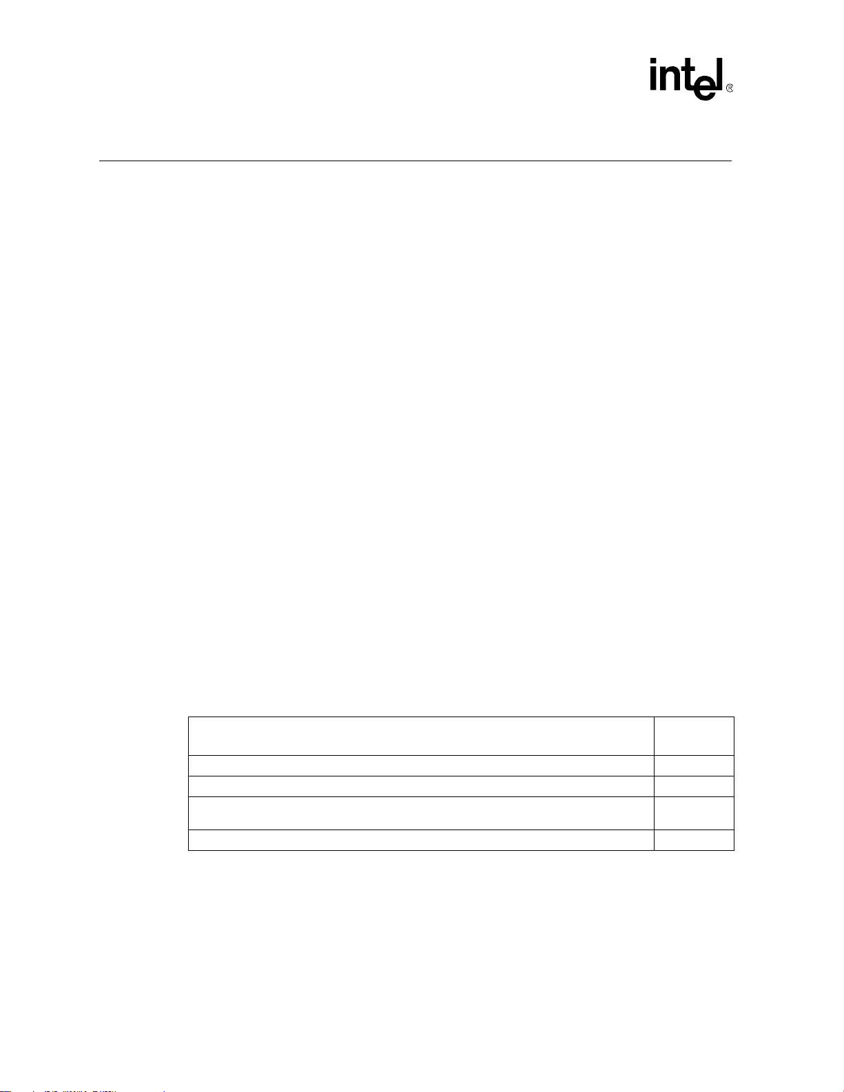
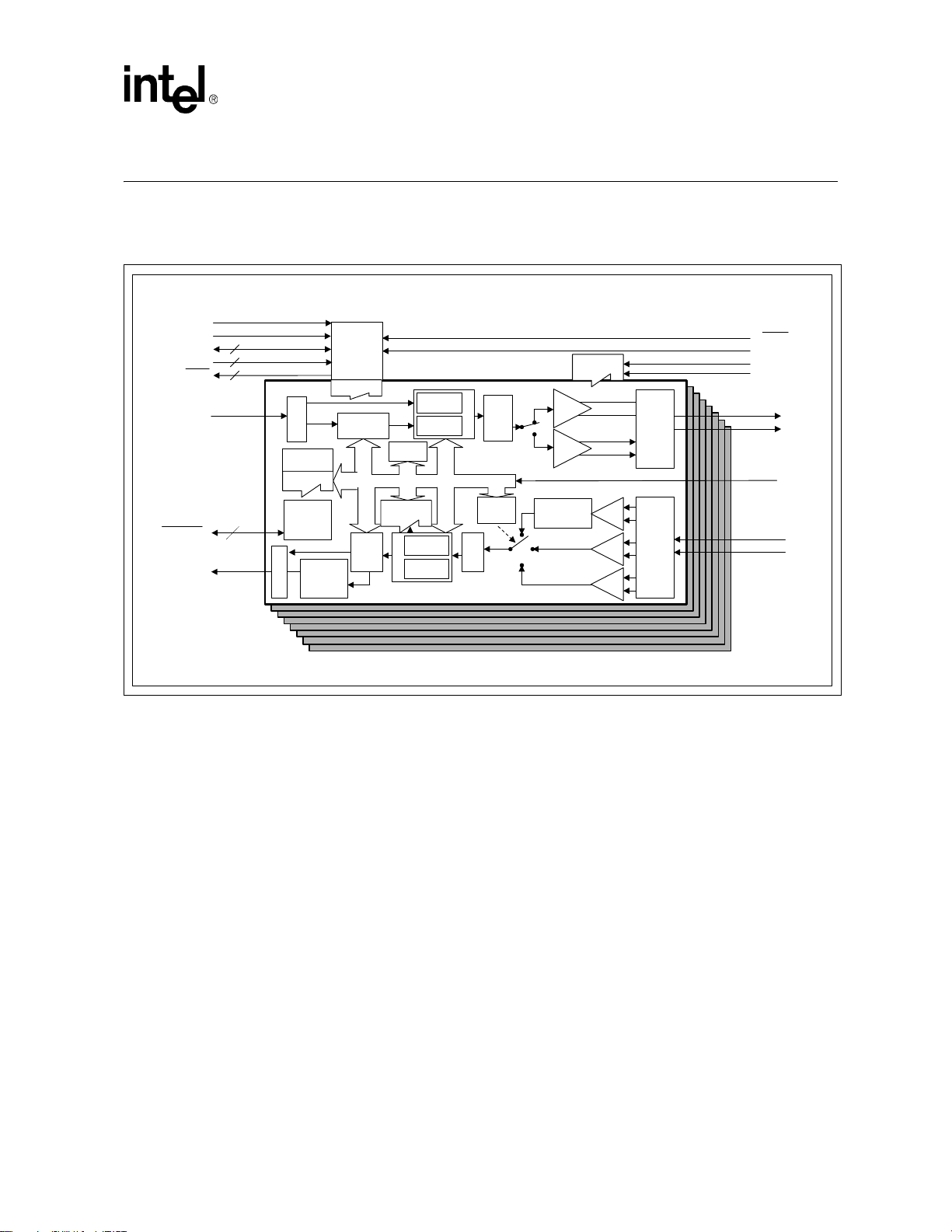
Figure 1 provides the LXT9785/LXT9785E block diagram.
Figure 1. Intel
®
LXT9785/LXT9785E Block Diagram
RMII/SMII Contr
ADD_<4:0>
MDIO
MDC
MDINT
TxDatan
LEDn_<2:0>
RxDatan
8-Port Global
Functions
Management /
TX PCS
Mgmt
Counters
Register Set
Port LED
Drivers
Carrier Sense
Data Valid
Error Detect
Mode Selec t
Logic & LED
Drivers
Register Set
Parallel/Serial
Converter
Serial to
Parallel
Converter
Manchester
Encoder
Scrambler
& Encoder
Auto
Negotiation
Clock Generator
Manchester
10
Decoder
Decoder &
100
Descrambler
Per-Port Functions
10
100
Slicer
Pulse
Shaper
Media
Select
TP
Driver
ECL
Driver
Adaptive EQ with BL
Wander Cancellation
PORT 0
PORT 1
PORT 2
PORT 3
Clock
Generator
+
-
+
-
PORT 4
PORT 5
PORT 6
100TX
100FX
10BT
PORT 7
+
-
+
-
+
-
TP /
Fiber
Out
TP /
Fiber In
2
2
2
3
RX PCS
RESET
PWRDN
REFCLK
SYNC (SMII only)
TPFOPn
TPFONn
Fiber
select n
TPFIPn
TPFINn
Datasheet 19
Document Number: 249241
Revision Number: 007
Revision Date: August 28, 2003
Page 18

Intel® LXT9785 and Intel® LXT9785E Advanced 8-Port 10/100 Mbps PHY Transceivers
3.0 Pin/Ball Assignments and Signal Descriptions
3.1 PQFP Pin Assignments
The following sections show PQFP pin assignments and signal descriptions:
• Section 3.1.1, “PQFP Pin Assignments – RMII Configuration” on page 21
• Section 3.1.2, “PQFP Pin Assignments – SMII Configuration” on page 26
• Section 3.1.3, “PQFP Pin Assignments – SS-SMII Configuration” on page 31
Table 1 lists the acronyms and descriptions for signal types.
Table 1. Intel
Acronym Description
®
LXT9785/LXT9785E Signal Type Descriptions
AI Analog Input
AO Analog Output
I Input
O Output
OD Open Drain Output
ST Schmitt Triggered Input
TS Three-State-able Output
SL Slew-rate Limited Output
IP Weak Internal Pull-Up
ID Weak Internal Pull-Down
20 Datasheet
Document Number: 249241
Revision Date: August 28, 2003
Revision Number: 007
Page 19
Intel® LXT9785 and Intel® LXT9785E Advanced 8-Port 10/100 Mbps PHY Transceivers
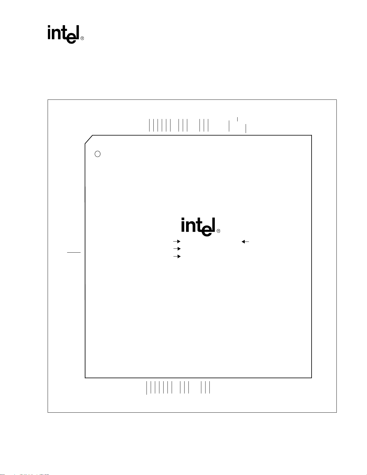
3.1.1 PQFP Pin Assignments – RMII Configuration
Figure 2 and Table 2, “Intel® LXT9785/LXT9785E RMII PQFP Pin List” on page 22 provide
LXT9785/LXT9785 RMII PQFP pin assignments.
Figure 2. Intel
CRS_DV6.......1
RxER6/LINKHOLD.. 2
TxEN6.......3
TxData6_0.......4
TxData6_1.......5
REFCLK1.......6
RxData5_1.......7
RxData5_0.......8
GNDIO.......9
CRS_DV5.......10
RxER5/FIFOSEL1.....11
TxEN5.......12
TxData5_0.......13
TxData5_1.......14
RxData4_1.......15
RxData4_0.......16
CRS_DV4.......17
VCCIO.......18
GNDIO.......19
RxER4/FIFOSEL0.....20
TxEN4.......21
TxData4_0.......22
TxData4_1.......23
MDC1.......24
MDIO1.......25
MDINT1.......26
RxData3_1.......27
RxData3_0.......28
VCCIO.......29
GNDIO.......30
CRS_DV3.......31
RxER3.......32
TxEN3.......33
TxData3_0.......34
TxData3_1.......35
RxData2_1.......36
RxData2_0.......37
GNDIO.......38
CRS_DV2.......39
RxER2/PREASEL .....40
TxEN2.......41
TxData2_0.......42
TxData2_1.......43
REFCLK0.......44
RxData1_1.......45
RxData1_0.......46
VCCIO.......47
GNDIO.......48
CRS_DV1.......49
RxER1/PAUSE.......50
TxEN1.......51
TxData1_0.......52
®
LXT9785 and Intel® LXT9785E RMII 208-Pin PQFP Assignments
208 ........ VCCIO
207 ........ GNDIO
206 ........ RxData6_0
205 ........ RxData6_1
204 ........ TxData7_1
203 ........ TxData7_0
202 ........ TxEN7
201 ........ RxER7
200 ........ CRS_DV7
199 ........ GNDIO
198 ........ RxData7_0
197 ........ RxData7_1
196 ........ VCCD
195 ........ GNDD
194 ........ LED7_3
193 ........ LED7_2
192 ........ LED7_1
191 ........ LED6_3
190 ........ LED6_2
189 ........ LED6_1
188 ........ GNDIO
187 ........ LED5_3
186 ........ LED5_2
185 ........ LED5_1
184 ........ VCCD
183 ........ GNDD
182 ........ LED4_3
181 ........ LED4_2
180 ........ LED4_1
179 ........ SGND
178 ........ ModeSel1
177 ........ ModeSel0
176 ........ Section
175 ........ RESET
Part #
LOT #
FPO #
LXT9785/9785E XX
XXXXXX
XXXXXXXX
174 ........ PWRDWN
173 ........ G_FX/TP
172 ........ N/C
171....... TRST
170 ........ TCK
169 ........ TMS
Rev #
168 ........ TDO
167 ........ TDI
166 ........ SD7
165 ........ SD6
164 ........ VCCPECL
163 ........ GNDPECL
162 ........ SD5
161 ........ SD4
160 ........ N/C
159 ........ N/C
158 ........ VCCR7
157 ........ TPFIP7
156 .........TPFIN7
155 .........GNDR7
154 .........TPFOP7
153 .........TPFON7
152 .........VCCT6/7
151 .........TPFON6
150 .........TPFOP6
149 .........GNDR6
148 .........GNDT6/7
147 .........TPFIN6
146 .........TPFIP6
145 .........VCCR6
144 .........VCCR5
143 .........TPFIP5
142 .........TPFIN5
141 .........GNDR5
140 .........TPFOP5
139 .........TPFON5
138 .........VCCT4/5
137 .........TPFON4
136 .........TPFOP4
135 .........GNDR4
134 .........GNDT4/5
133 .........TPFIN4
132 .........TPFIP4
131 .........VCCR4
130 .........VCCR3
129 .........TPFIP3
128 .........TPFIN3
127 .........GNDT2/3
126 .........GNDR3
125 .........TPFOP3
124 .........TPFON3
123 .........VCCT2/3
122 .........TPFON2
121 .........TPFOP2
120 .........GNDR2
119 .........TPFIN2
118 .........TPFIP2
117 .........VCCR2
116 .........VCCR1
115 .........TPFIP1
114 .........TPFIN1
113 .........GNDT0/1
112 .........GNDR1
111 .........TPFOP1
110 .........TPFON1
109 .........VCCT0/1
108 .........TPFON0
107 .........TPFOP0
106 .........GNDR0
105 .........TPFIN0
SD0 ...... 96
MDC0 ...... 63
VCCD ...... 65
TxEN0 ...... 60
VCCIO ...... 56
GNDIO ...... 57
TxData1_1 ...... 53
CRS_DV0 ...... 58
RxData0_1 ...... 54
RxData0_0 ...... 55
TxData0_0 ...... 61
RxER0/MDIX ...... 59
GNDD ...... 66
MDIO0 ...... 64
LED3_3 ......68
LED3_2 ......69
LED3_1 ......70
LED2_3 ......71
LED2_2 ......72
TxData0_1 ...... 62
MDINT0 ......67
LED2_1 ......73
VCCD ...... 78
GNDIO ...... 74
GNDD ...... 79
LED1_3 ......75
LED1_2 ......76
LED1_1 ......77
LED0_3 ......80
CFG_3 ...... 85
CFG_2 ...... 86
CFG_1 ...... 87
ADD_4 ......88
ADD_3 ......89
ADD_2 ......90
ADD_1 ......91
MDDIS ...... 84
LED0_2 ......81
LED0_1 ......82
AMDIX_EN ...... 83
ADD_0 ......92
SD1 ...... 97
SD_2P5V ...... 95
TxSlew_1 ...... 93
TxSlew_0 ...... 94
N/C ...... 102
SD2 ...... 100
SD3 ...... 101
TPFIP0 ...... 104
VCCPECL ...... 98
VCCR0 ...... 103
GNDPECL ...... 99
Datasheet 21
Document Number: 249241
Revision Number: 007
Revision Date: August 28, 2003
Page 20
Intel® LXT9785 and Intel® LXT9785E Advanced 8-Port 10/100 Mbps PHY Transceivers
Table 2. Intel® LXT9785/LXT9785E RMII PQFP Pin List
Pin Symbol Type
Reference for Full
Description
Pin Symbol Type
Reference for Full
Description
1 CRS_DV6
RxER6/
2
LINKHOLD
3 TxEN6 I, ID Table 5 (page 36)
4 TxData6_0 I, ID Table 5 (page 36)
5 TxData6_1 I, ID Table 5 (page 36)
6 REFCLK1 I Table 5 (page 36)
7 RxData5_1
8 RxData5_0 O, TS Table 5 (page 36)
9GNDIO – Table 15 (page 48)
10 CRS_DV5
RxER5 /
11
FIFOSEL1
12 TxEN5 I, ID Table 5 (page 36)
13 TxData5_0 I, ID Table 5 (page 36)
14 TxData5_1 I, ID Table 5 (page 36)
15 RxData4_1
16 RxData4_0 O, TS Table 5 (page 36)
17 CRS_DV4
18 VCCIO – Table 15 (page 48)
19 GNDIO – Table 15 (page 48)
RxER4 /
20
FIFOSEL0
21 TxEN4 I, ID Table 5 (page 36)
22 TxData4_0 I, ID Table 5 (page 36)
23 TxData4_1 I, ID Table 5 (page 36)
24 MDC1 I, ST, ID Table 8 (page 40)
25 MDIO1
26 MDINT1
27 RxData3_1
28 RxData3_0 O, TS Table 5 (page 36)
29 VCCIO – Table 15 (page 48)
O, TS,
SL
O, TS,
SL, ID,
I, ST
O, TS,
ID
O, TS,
SL
O, TS,
SL, ID,
I, ST
O,
TS,ID
O, TS,
SL
O, TS,
SL, ID,
I, ST
I/O, TS,
SL, IP
OD, TS,
SL, IP
O, TS,
ID
Table 5 (page 36)
Table 5 (page 36)
Table 5 (page 36)
Table 5 (page 36)
Table 5 (page 36)
Table 5 (page 36)
Table 5 (page 36)
Table 5 (page 36)
Table 8 (page 40)
Table 8 (page 40)
Table 5 (page 36)
30 GNDIO – Table 15 (page 48)
31 CRS_DV3
32 RxER3
33 TxEN3 I, ID Table 5 (page 36)
34 TxData3_0 I, ID Table 5 (page 36)
35 TxData3_1 I, ID Table 5 (page 36)
36 RxData2_1
37 RxData2_0 O, TS Table 5 (page 36)
38 GNDIO – Table 15 (page 48)
39 CRS_DV2
RxER2
40
(PREASEL)
41 TxEN2 I, ID Table 5 (page 36)
42 TxData2_0 I, ID Table 5 (page 36)
43 TxData2_1 I, ID Table 5 (page 36)
44 REFCLK0 I Table 5 (page 36)
45 RxData1_1
46 RxData1_0 O, TS Table 5 (page 36)
47 VCCIO – Table 15 (page 48)
48 GNDIO – Table 15 (page 48)
49 CRS_DV1
RxER1/
50
PAU SE
51 TxEN1 I, ID Table 5 (page 36)
52 TxData1_0 I, ID Table 5 (page 36)
53 TxData1_1 I, ID Table 5 (page 36)
54 RxData0_1
55 RxData0_0 O, TS Table 5 (page 36)
56 VCCIO – Table 15 (page 48)
57 GNDIO – Table 15 (page 48)
58 CRS_DV0
O, TS,
SL
O, TS,
SL, ID
O, TS,
ID
O, TS,
SL
O, TS,
SL, ID,
I, ST
O, TS,
ID
O, TS,
SL
O, TS,
SL, ID,
I, ST
O, TS,
ID
O, TS,
SL
Table 5 (page 36)
Table 5 (page 36)
Table 5 (page 36)
Table 5 (page 36)
Table 5 (page 36)
Table 5 (page 36)
Table 5 (page 36)
Table 5 (page 36)
Table 5 (page 36)
Table 5 (page 36)
22 Datasheet
Document Number: 249241
Revision Date: August 28, 2003
Revision Number: 007
Page 21

Intel® LXT9785 and Intel® LXT9785E Advanced 8-Port 10/100 Mbps PHY Transceivers
Pin Symbol Type
RxER0/
59
MDIX
60 TxEN0 I, ID Table 5 (page 36)
61 TxData0_0 I, ID Table 5 (page 36)
62 TxData0_1 I, ID Table 5 (page 36)
63 MDC0 I, ST, ID Table 8 (page 40)
64 MDIO0
65 VCCD – Table 15 (page 48)
66 GNDD – Table 15 (page 48)
67 MDINT0
68 LED3_3
69 LED3_2
70 LED3_1
71 LED2_3
72 LED2_2
73 LED2_1
74 GNDIO – Table 15 (page 48)
75 LED1_3
76 LED1_2
77 LED1_1
78 VCCD – Table 15 (page 48)
79 GNDD – Table 15 (page 48)
80 LED0_3
81 LED0_2
82 LED0_1
83 AMDIX_EN I, ST, IP Table 13 (page 43)
84 MDDIS I, ST, ID Table 9 (page 41)
85 CFG_3 I, ST, ID Table 13 (page 43)
86 CFG_2 I, ST, ID Table 13 (page 43)
O, TS,
SL, ID,
I, ST
I/O, TS,
SL, IP
OD, TS,
SL, IP
OD, TS,
SO, IP
OD, TS,
SL, IP
OD, TS,
SL, IP
OD, TS,
SL, IP
OD, TS,
SL, IP
OD, TS,
SL, IP
OD, TS,
SL, IP
OD, TS,
SL, IP
OD, TS,
SL, IP
OD, TS,
SL, IP
OD, TS,
SL, IP
OD, TS,
SL, IP
Reference for Full
Description
Table 5 (page 36)
Table 8 (page 40)
Table 8 (page 40)
Table 14 (page 47)
Table 14 (page 47)
Table 14 (page 47)
Table 14 (page 47)
Table 14 (page 47)
Table 14 (page 47)
Table 14 (page 47)
Table 14 (page 47)
Table 14 (page 47)
Table 14 (page 47)
Table 14 (page 47)
Table 14 (page 47)
Pin Symbol Type
87 CFG_1 I, ST, ID Table 13 (page 43)
88 ADD_4 I, ST, ID Table 13 (page 43)
89 ADD_3 I, ST, ID Table 13 (page 43)
90 ADD_2 I, ST, ID Table 13 (page 43)
91 ADD_1 I, ST, ID Table 13 (page 43)
92 ADD_0 I, ST, ID Table 13 (page 43)
93 TxSLEW_1 I, ST, ID Table 13 (page 43)
94 TxSLEW_0 I, ST, ID Table 13 (page 43)
95 SD_2P5V I, ST, ID Table 10 (page 42)
96 SD0 I Table 10 (page 42)
97 SD1 I Table 10 (page 42)
98 VCCPECL – Table 15 (page 48)
99 GNDPECL – Table 15 (page 48)
100 SD2 I Table 10 (page 42)
101 SD3 I Table 10 (page 42)
102 N/C – Table 17 (page 50)
103 VCCR0 – Table 15 (page 48)
104 TPFIP0 AO/AI Table 11 (page 42)
105 TPFIN0 AO/AI Table 11 (page 42)
106 GNDR0 – Table 15 (page 48)
107 TPFOP0 AO/AI Table 11 (page 42)
108 TPFON0 AO/AI Table 11 (page 42)
109 VCCT0/1 – Table 15 (page 48)
110 TPFON1 AO/AI Table 11 (page 42)
111 TPFOP1 AO/AI Table 11 (page 42)
112 GNDR1 – Table 15 (page 48)
113 GN DT0 /1 – Table 15 (page 48)
114 TPFIN1 AO/AI Table 11 (page 42)
115 TPFIP1 AO/AI Table 11 (page 42)
116 VCCR1 – Table 15 (page 48)
117 VCCR2 – Table 15 (page 48)
118 TPFIP2 AO/AI Table 11 (page 42)
119 TPFIN2 AO/AI Table 11 (page 42)
120 GNDR2 – Table 15 (page 48)
121 TPFOP2 AO/AI Table 11 (page 42)
122 TPFON2 AO/AI Table 11 (page 42)
123 VCCT2/3 – Table 15 (page 48)
124 TPFON3 AO/AI Table 11 (page 42)
Reference for Full
Description
Datasheet 23
Document Number: 249241
Revision Number: 007
Revision Date: August 28, 2003
Page 22
Intel® LXT9785 and Intel® LXT9785E Advanced 8-Port 10/100 Mbps PHY Transceivers
Pin Symbol Type
125 TPFOP3 AO/AI Table 11 (page 42)
126 GNDR3 – Table 15 (page 48)
127 GNDT2/3 – Table 15 (page 48)
128 TPFIN3 AO/AI Table 11 (page 42)
129 TPFIP3 AO/AI Table 11 (page 42)
130 VCCR3 – Table 15 (page 48)
131 VCCR4 – Table 15 (page 48)
132 TPFIP4 AO/AI Table 11 (page 42)
133 TPFIN4 AO/AI Table 11 (page 42)
134 GNDT4/5 – Table 15 (page 48)
135 GNDR4 – Table 15 (page 48)
136 TPFOP4 AO/AI Table 11 (page 42)
137 TPFON4 AO/AI Table 11 (page 42)
138 VCCT4/5 – Table 15 (page 48)
139 TPFON5 AO/AI Table 11 (page 42)
140 TPFOP5 AO/AI Table 11 (page 42)
141 GNDR5 – Table 15 (page 48)
142 TPFIN5 AO/AI Table 11 (page 42)
143 TPFIP5 AO/AI Table 11 (page 42)
144 VCCR5 – Table 15 (page 48)
145 VCCR6 – Table 15 (page 48)
146 TPFIP6 AO/AI Table 11 (page 42)
147 TPFIN6 AO/AI Table 11 (page 42)
148 GNDT6/7 – Table 15 (page 48)
149 GNDR6 – Table 15 (page 48)
150 TPFOP6 AO/AI Table 11 (page 42)
151 TPFON6 AO/AI Table 11 (page 42)
152 VCCT6/7 – Table 15 (page 48)
153 TPFON7 AO/AI Table 11 (page 42)
154 TPFOP7 AO/AI Table 11 (page 42)
155 GNDR7 – Table 15 (page 48)
156 TPFIN7 AO/AI Table 11 (page 42)
157 TPFIP7 AO/AI Table 11 (page 42)
158 VCCR7 – Table 15 (page 48)
159 N/C – Table 17 (page 50)
160 N/C – Table 17 (page 50)
161 SD4 I Table 10 (page 42)
162 SD5 I Table 10 (page 42)
Reference for Full
Description
Pin Symbol Type
163 GNDPECL – Table 15 (page 48)
164 VCCPECL – Table 15 (page 48)
165 SD6 I Table 10 (page 42)
166 SD7 I Table 10 (page 42)
167 TDI I, ST, IP Table 12 (page 43)
168 TDO O, TS Table 12 (page 43)
169 TMS I, ST, IP Table 12 (page 43)
170 TCK I, ST, ID Table 12 (page 43)
171 TRST
172 N/C – Table 17 (page 50)
173 G_FX/TP
174 PWRDWN I, ST, ID Table 13 (page 43)
175 RESET
176 SECTION I, ST, ID Table 13 (page 43)
177 ModeSel0 I, ST, ID Table 13 (page 43)
178 ModeSel1 I, ST, ID Table 13 (page 43)
179 SGND – Table 15 (page 48)
180 LED4_1
181 LED4_2
182 LED4_3
183 GNDD – Table 15 (page 48)
184 VCCD – Table 15 (page 48)
185 LED5_1
186 LED5_2
187 LED5_3
188 GNDIO – Table 15 (page 48)
189 LED6_1
190 LED6_2
191 LED6_3
192 LED7_1
193 LED7_2
I, ST, IP Table 12 (page 43)
I, ST, ID Table 13 (page 43)
I, ST, IP Table 13 (page 43)
OD, TS,
SL, IP
OD, TS,
SL, IP
OD, TS,
SL, IP
OD, TS,
SL, IP
OD, TS,
SL, IP
OD, TS,
SL, IP
OD, TS,
SL, IP
OD, TS,
SL, IP
OD, TS,
SL, IP
OD, TS,
SL, IP
OD, TS,
SL, IP
Reference for Full
Description
Table 14 (page 47)
Table 14 (page 47)
Table 14 (page 47)
Table 14 (page 47)
Table 14 (page 47)
Table 14 (page 47)
Table 14 (page 47)
Table 14 (page 47)
Table 14 (page 47)
Table 14 (page 47)
Table 14 (page 47)
24 Datasheet
Document Number: 249241
Revision Date: August 28, 2003
Revision Number: 007
Page 23
Intel® LXT9785 and Intel® LXT9785E Advanced 8-Port 10/100 Mbps PHY Transceivers
Pin Symbol Type
194 LED7_3
195 GNDD – Table 15 (page 48)
196 VCCD – Table 15 (page 48)
197 RxData7_1
198 RxData7_0 O, TS Table 5 (page 36)
199 GNDIO – Table 15 (page 48)
200 CRS_DV7
201 RxER7
202 TxEN7 I, ID Table 5 (page 36)
203 TxData7_0 I, ID Table 5 (page 36)
204 TxData7_1 I, ID Table 5 (page 36)
205 RxData6_1
206 RxData6_0 O, TS Table 5 (page 36)
207 GNDIO – Table 15 (page 48)
208 VCCIO – Table 15 (page 48)
OD, TS,
SL, IP
O, TS,
ID
O, TS,
SL
O, TS,
SL, ID
O, TS,
ID
Reference for Full
Description
Table 5 (page 36)
Table 5 (page 36)
Table 5 (page 36)
Table 5 (page 36)
Table 5 (page 36)
Datasheet 25
Document Number: 249241
Revision Number: 007
Revision Date: August 28, 2003
Page 24
Intel® LXT9785 and Intel® LXT9785E Advanced 8-Port 10/100 Mbps PHY Transceivers
3.1.2 PQFP Pin Assignments – SMII Configuration
Figure 3 and Table 3, “Intel® LXT9785/LXT9785E SMII PQFP Pin List” on page 27 provide the
LXT9785/LXT9785E SMII PQFP pin assignments.
Figure 3. Intel
LINKHOLD .......2
N/C.......1
N/C.......3
TxData6.......4
N/C.......5
REFCLK1.......6
N/C.......7
RxData5.......8
GNDIO.......9
N/C.......10
FIFOSEL1.......11
N/C.......12
TxData5.......13
N/C.......14
N/C.......15
RxData4.......16
N/C.......17
VCCIO.......18
GNDIO.......19
FIFOSEL0.......20
N/C.......21
TxData4.......22
N/C.......23
MDC1.......24
MDIO1.......25
MDINT1.......26
N/C.......27
RxData3.......28
VCCIO.......29
GNDIO.......30
N/C.......31
N/C.......32
N/C.......33
TxData3.......34
SYNC0.......35
N/C.......36
RxData2.......37
GNDIO.......38
N/C.......39
PREASEL.......40
N/C.......41
TxData2.......42
N/C.......43
REFCLK0.......44
N/C.......45
RxData1.......46
VCCIO.......47
GNDIO.......48
N/C.......49
PAUSE.......50
N/C.......51
TxData1.......52
®
LXT9785/LXT9785E SMII 208-Pin PQFP Assignments
208 ........ VCCIO
207 ........ GNDIO
206 ........ RxData6
205 ........ N/C
204 ........ SYNC1
203 ........ TxData7
202 ........ N/C
201 ........ N/C
200 ........ N/C
199 ........ GNDIO
198 ........ RxData7
197 ........ N/C
196 ........ VCCD
195 ........ GNDD
194 ........ LED7_3
193 ........ LED7_2
192 ........ LED7_1
191 ........ LED6_3
190 ........ LED6_2
189 ........ LED6_1
188 ........ GNDIO
187 ........ LED5_3
186 ........ LED5_2
185 ........ LED5_1
184 ........ VCCD
183 ........ GNDD
182 ........ LED4_3
181 ........ LED4_2
180 ........ LED4_1
179 ........ SGND
178 ........ ModeSel_1
177 ........ ModeSel_0
Part #
LOT #
FPO #
LXT9785/9785E XX
XXXXXX
XXXXXXXX
176 ........ Section
175 ........ RESET
174 ........ PWRDWN
173 ........ G_FX/TP
172 ........ N/C
171....... TRST
Rev #
170 ........ TCK
169 ........ TMS
168 ........ TDO
167 ........ TDI
166 ........ SD7
165 ........ SD6
164 ........ VCCPECL
163 ........ GNDPECL
162 ........ SD5
161 ........ SD4
160 ........ N/C
159 ........ N/C
158 ........ VCCR7
157 ........ TPFIP7
156 ........ TPFIN7
155 ........ GNDR7
154 ........ TPFOP7
153 ........ TPFON7
152 ........ VCCT6/7
151 ........ TPFON6
150 ........ TPFOP6
149 ........ GNDR6
148 ........ GNDT6/7
147 ........ TPFIN6
146 ........ TPFIP6
145 ........ VCCR6
144 ........ VCCR5
143 ........ TPFIP5
142 ........ TPFIN5
141 ........ GNDR5
140 ........ TPFOP5
139 ........ TPFON5
138 ........ VCCT4/5
137 ........ TPFON4
136 ........ TPFOP4
135 ........ GNDR4
134 ........ GNDT4/5
133 ........ TPFIN4
132 ........ TPFIP4
131 ........ VCCR4
130 ........ VCCR3
129 ........ TPFIP3
128 ........ TPFIN3
127 ........ GNDT2/3
126 ........ GNDR3
125 ........ TPFOP3
124 ........ TPFON3
123 ........ VCCT2/3
122 ........ TPFON2
121 ........ TPFOP2
120 ........ GNDR2
119 ........ TPFIN2
118 ........ TPFIP2
117 ........ VCCR2
116 ........ VCCR1
115 ........ TPFIP1
114 ........ TPFIN1
113 ........ GNDT0/1
112 ........ GNDR1
111 ........ TPFOP1
110 ........ TPFON1
109 ........ VCCT0/1
108 ........ TPFON0
107 ........ TPFOP0
106 ........ GNDR0
105 ........ TPFIN0
N/C ......53
N/C ......54
N/C ......58
N/C ......60
N/C ......62
MDIX ......59
MDC0 ......63
VCCD ......65
VCCIO ......56
GNDIO ......57
RxData0 ......55
TxData0 ......61
GNDD ......66
MDIO0 ......64
LED3_3 ......68
LED3_2 ......69
LED3_1 ......70
LED2_3 ......71
LED2_2 ......72
MDINT0 ......67
LED2_1 ......73
VCCD ......78
GNDIO ......74
GNDD ......79
LED1_3 ......75
LED1_2 ......76
LED1_1 ......77
LED0_3 ......80
CFG_3 ......85
CFG_2 ......86
CFG_1 ......87
ADD_4 ......88
ADD_3 ......89
ADD_2 ......90
MDDIS ......84
LED0_2 ......81
LED0_1 ......82
AMDIX_EN ......83
ADD_1 ......91
SD0 ......96
ADD_0 ......92
SD1 ......97
SD_2P5V ......95
TxSlew_1 ......93
TxSlew_0 ......94
N/C ......102
SD2 ......100
SD3 ......101
TPFIP0 ......104
VCCPECL ......98
VCCR0 ......103
GNDPECL ......99
26 Datasheet
Document Number: 249241
Revision Date: August 28, 2003
Revision Number: 007
Page 25

Intel® LXT9785 and Intel® LXT9785E Advanced 8-Port 10/100 Mbps PHY Transceivers
Table 3. Intel® LXT9785/LXT9785E SMII PQFP Pin List
Reference for Full
Pin Symbol Type
1
Description
Pin Symbol Type
Reference for Full
1
Description
1N/C – Table 16 (page 50)
N/C
2
(LINKHOLD)
–
I, ID,
Table 16 (page 50)
3N/C – Table 16 (page 50)
4 TxData6 I, ID Table 6 (page 39)
5N/C – Table 16 (page 50)
6 REFCLK1 I Table 5 (page 36)
7N/C – Table 16 (page 50)
8 RxData5 O, TS Table 6 (page 39)
9 GNDIO – Table 15 (page 48)
10 N/C – Table 16 (page 50)
11 F IFO SEL1
I, ID,
ST
Table 16 (page 50)
12 N/C – Table 16 (page 50)
13 TxData5 I, ID Table 6 (page 39)
14 N/C – Table 16 (page 50)
15 N/C – Table 16 (page 50)
16 RxData4 O, TS Table 6 (page 39)
17 N/C – Table 16 (page 50)
18 VCCIO – Table 15 (page 48)
19 GNDIO – Table 15 (page 48)
20 FIFOSEL0
I, ID,
ST
Table 16 (page 50)
21 N/C I, ID Table 16 (page 50)
22 TxData4 I, ID Table 6 (page 39)
23 N/C – Table 16 (page 50)
24 MDC1 I, ST, ID Table 9 (page 41)
25 MDIO1
I/O, TS,
SL, IP
Table 9 (page 41)
OD,
26 MDINT1
TS, SL, IPTable 9 (page 41)
27 N/C – Table 16 (page 50)
28 RxData3 O, TS Table 6 (page 39)
29 VCCIO – Table 15 (page 48)
30 GNDIO – Table 15 (page 48)
31 N/C – Table 16 (page 50)
32 N/C – Table 16 (page 50)
33 N/C – Table 16 (page 50)
34 TxData3 I, ID Table 6 (page 39)
35 SYNC0 I, ID Table 7 (page 39)
36 N/C – Table 16 (page 50)
37 RxData2 O, TS Table 6 (page 39)
38 GNDIO – Table 15 (page 48)
39 N/C – Table 16 (page 50)
40 PREASEL
I, ID,
ST
Table 16 (page 50)
41 N/C – Table 16 (page 50)
42 TxData2 I, ID Table 6 (page 39)
43 N/C – Table 16 (page 50)
44 REFCLK0 I Table 5 (page 36)
45 N/C – Table 16 (page 50)
46 RxData1 O, TS Table 6 (page 39)
47 VCCIO – Table 15 (page 48)
48 GNDIO – Table 15 (page 48)
49 N/C – Table 16 (page 50)
50 PAUSE
I, ID,
ST
Table 13 (page 43)
51 N/C – Table 16 (page 50)
52 TxData1 I, ID Table 6 (page 39)
53 N/C – Table 16 (page 50)
54 N/C – Table 16 (page 50)
55 RxData0 O, TS Table 6 (page 39)
56 VCCIO – Table 15 (page 48)
57 GNDIO – Table 15 (page 48)
58 N/C – Table 16 (page 50)
59 MDIX
I, ID,
ST
Table 13 (page 43)
60 N/C – Table 16 (page 50)
61 TxData0 I, ID Table 6 (page 39)
62 N/C – Table 16 (page 50)
63 MDC0 I, ST, ID Table 9 (page 41)
64 MDIO0
I/O, TS,
SL, IP
Table 9 (page 41)
65 VCCD – Table 15 (page 48)
66 GNDD – Table 15 (page 48)
OD,
67 MDINT0
TS, SL, IPTable 9 (page 41)
Datasheet 27
Document Number: 249241
Revision Number: 007
Revision Date: August 28, 2003
Page 26
Intel® LXT9785 and Intel® LXT9785E Advanced 8-Port 10/100 Mbps PHY Transceivers
Reference for Full
Pin Symbol Type
1
Description
OD,
TS,
68 LED3_3
Table 14 (page 47)
SO, IP
OD,
69 LED3_2
TS, SL, IPTable 14 (page 47)
OD,
70 LED3_1
TS, SL, IPTable 14 (page 47)
OD,
71 LED2_3
TS, SL, IPTable 14 (page 47)
OD,
72 LED2_2
TS, SL, IPTable 14 (page 47)
OD,
73 LED2_1
TS, SL, IPTable 14 (page 47)
74 GNDIO – Table 15 (page 48)
OD,
75 LED1_3
TS, SL, IPTable 14 (page 47)
OD,
76 LED1_2
TS, SL, IPTable 14 (page 47)
OD,
77 LED1_1
TS, SL, IPTable 14 (page 47)
78 VCCD – Table 15 (page 48)
79 GNDD – Table 15 (page 48)
OD,
80 LED0_3
TS, SL, IPTable 14 (page 47)
OD,
81 LED0_2
TS, SL, IPTable 14 (page 47)
OD,
82 LED0_1
TS, SL, IPTable 14 (page 47)
83 AMDIX_EN I, ST, IP Table 13 (page 43)
84 MDDIS I, ST, ID Table 8 (page 40)
85 CFG_3 I, ST, ID Table 13 (page 43)
86 CFG_2 I, ST, ID Table 13 (page 43)
87 CFG_1 I, ST, ID Table 13 (page 43)
88 ADD_4 I, ST, ID Table 13 (page 43)
89 ADD_3 I, ST, ID Table 13 (page 43)
90 ADD_2 I, ST, ID Table 13 (page 43)
91 ADD_1 I, ST, ID Table 13 (page 43)
Reference for Full
Pin Symbol Type
1
Description
92 ADD_0 I, ST, ID Table 13 (page 43)
93 TxSLEW_1 I, ST, ID Table 13 (page 43)
94 TxSLEW_0 I, ST, ID Table 13 (page 43)
95 SD_2P5V I, ST, ID Table 10 (page 42)
96 SD0 I Table 10 (page 42)
97 SD1 I Table 10 (page 42)
98 VCCPECL – Table 15 (page 48)
99 GNDPECL – Table 15 (page 48)
100 SD2 I Table 10 (page 42)
101 SD3 I Table 10 (page 42)
102 N/C – Table 17 (page 50)
103 VCCR0 – Table 15 (page 48)
104 TPFIP0 AI/AO Table 11 (page 42)
105 TPFIN0 AI/AO Table 11 (page 42)
106 GNDR0 – Table 15 (page 48)
107 TPFOP0 AO/AI Table 11 (page 42)
108 TPFON0 AO/AI Table 11 (page 42)
109 VCCT0/1 – Table 15 (page 48)
110 TPFON1 AO/AI Table 11 (page 42)
111 TPFOP1 AO/AI Table 11 (page 42)
112 GNDR1 – Table 15 (page 48)
113 G NDT0/1 – Table 15 (page 48)
114 TPFIN1 AI/AO Table 11 (page 42)
115 TPFIP1 AI/AO Table 11 (page 42)
116 VCCR1 – Table 15 (page 48)
117 VCCR2 – Table 15 (page 48)
118 TPFIP2 AI/AO Table 11 (page 42)
119 TPFIN2 AI/AO Table 11 (page 42)
120 GNDR2 – Table 15 (page 48)
121 TPFOP2 AO/AI Table 11 (page 42)
122 TPFON2 AO/AI Table 11 (page 42)
123 VCCT2/3 – Table 15 (page 48)
124 TPFON3 AO/AI Table 11 (page 42)
125 TPFOP3 AO/AI Table 11 (page 42)
126 GNDR3 – Table 15 (page 48)
127 GNDT2/3 – Table 15 (page 48)
128 TPFIN3 AI/AO Table 11 (page 42)
129 TPFIP3 AI/AO Table 11 (page 42)
28 Datasheet
Document Number: 249241
Revision Date: August 28, 2003
Revision Number: 007
Page 27

Intel® LXT9785 and Intel® LXT9785E Advanced 8-Port 10/100 Mbps PHY Transceivers
Reference for Full
Pin Symbol Type
1
Description
130 VCCR3 – Table 15 (page 48)
131 VCCR4 – Table 15 (page 48)
132 TPFIP4 AI/AO Table 11 (page 42)
133 TPFIN4 AI/AO Table 11 (page 42)
134 GNDT4/5 – Table 15 (page 48)
135 GNDR4 – Table 15 (page 48)
136 TPFOP4 AO/AI Table 11 (page 42)
137 TPFON4 AO/AI Table 11 (page 42)
138 VCCT4/5 – Table 15 (page 48)
139 TPFON5 AO/AI Table 11 (page 42)
140 TPFOP5 AO/AI Table 11 (page 42)
141 GNDR5 – Table 15 (page 48)
142 TPFIN5 AI/AO Table 11 (page 42)
143 TPFIP5 AI/AO Table 11 (page 42)
144 VCCR5 – Table 15 (page 48)
145 VCCR6 – Table 15 (page 48)
146 TPFIP6 AI/AO Table 11 (page 42)
147 TPFIN6 AI/AO Table 11 (page 42)
148 GNDT6/7 – Table 15 (page 48)
149 GNDR6 – Table 15 (page 48)
150 TPFOP6 AO/AI Table 11 (page 42)
151 TPFON6 AO/AI Table 11 (page 42)
152 VCCT6/7 – Table 15 (page 48)
153 TPFON7 AO/AI Table 11 (page 42)
154 TPFOP7 AO/AI Table 11 (page 42)
155 GNDR7 – Table 15 (page 48)
156 TPFIN7 AI/AO Table 11 (page 42)
157 TPFIP7 AI/AO Table 11 (page 42)
158 VCCR7 – Table 15 (page 48)
159 N/C – Table 17 (page 50)
160 N/C – Table 17 (page 50)
161 SD4 I Table 10 (page 42)
162 SD5 I Table 10 (page 42)
163 GNDPECL – Table 15 (page 48)
164 VCCPECL – Table 15 (page 48)
165 SD6 I Table 10 (page 42)
166 SD7 I Table 10 (page 42)
167 TDI I, ST, IP Table 12 (page 43)
Reference for Full
Pin Symbol Type
1
Description
168 TDO O, TS Table 12 (page 43)
169 TMS I, ST, IP Table 12 (page 43)
170 TCK I, ST, ID Table 12 (page 43)
171 TRST
I, ST, IP Table 12 (page 43)
172 N/C – Table 17 (page 50)
173 G_FX/TP
I, ST, ID Table 13 (page 43)
174 PWRDWN I, ST, ID Table 13 (page 43)
175 RESET
I, ST, IP Table 13 (page 43)
176 Section I, ST, ID Table 13 (page 43)
177 ModeSel0 I, ST, ID Table 13 (page 43)
178 ModeSel1 I, ST, ID Table 13 (page 43)
179 SGND – Table 15 (page 48)
OD,
180 LED4_1
TS, SL, IPTable 14 (page 47)
OD,
181 LED4_2
TS, SL, IPTable 14 (page 47)
OD,
182 LED4_3
TS, SL, IPTable 14 (page 47)
183 GNDD – Table 15 (page 48)
184 VCCD – Table 15 (page 48)
OD,
185 LED5_1
TS, SL, IPTable 14 (page 47)
OD,
186 LED5_2
TS, SL, IPTable 14 (page 47)
OD,
187 LED5_3
TS, SL, IPTable 14 (page 47)
188 GNDIO – Table 15 (page 48)
OD,
189 LED6_1
TS, SL, IPTable 14 (page 47)
OD,
190 LED6_2
TS, SL, IPTable 14 (page 47)
OD,
191 LED6_3
TS, SL, IPTable 14 (page 47)
OD,
192 LED7_1
TS, SL, IPTable 14 (page 47)
Datasheet 29
Document Number: 249241
Revision Number: 007
Revision Date: August 28, 2003
Page 28
Intel® LXT9785 and Intel® LXT9785E Advanced 8-Port 10/100 Mbps PHY Transceivers
Reference for Full
Pin Symbol Type
193 LED7_2
1
Description
OD,
TS, SL, IPTable 14 (page 47)
194 LED7_3
TS, SL, IPTable 5 (page 36)
195 GNDD – Table 15 (page 48)
196 VCCD – Table 15 (page 48)
OD,
197 N/C
O, TS,
ID
Table 16 (page 50)
198 RxData7 O, TS Table 6 (page 39)
199 GNDIO – Table 15 (page 48)
200 N/C – Table 16 (page 50)
201 N/C – Table 16 (page 50)
202 N/C – Table 16 (page 50)
203 TxData7 I, ID Table 6 (page 39)
204 SYNC1 I, ID Table 5 (page 36)
205 N/C – Table 16 (page 50)
206 RxData6 O, TS Table 6 (page 39)
207 GNDIO – Table 15 (page 48)
208 VCCIO – Table 15 (page 48)
30 Datasheet
Document Number: 249241
Revision Date: August 28, 2003
Revision Number: 007
Page 29
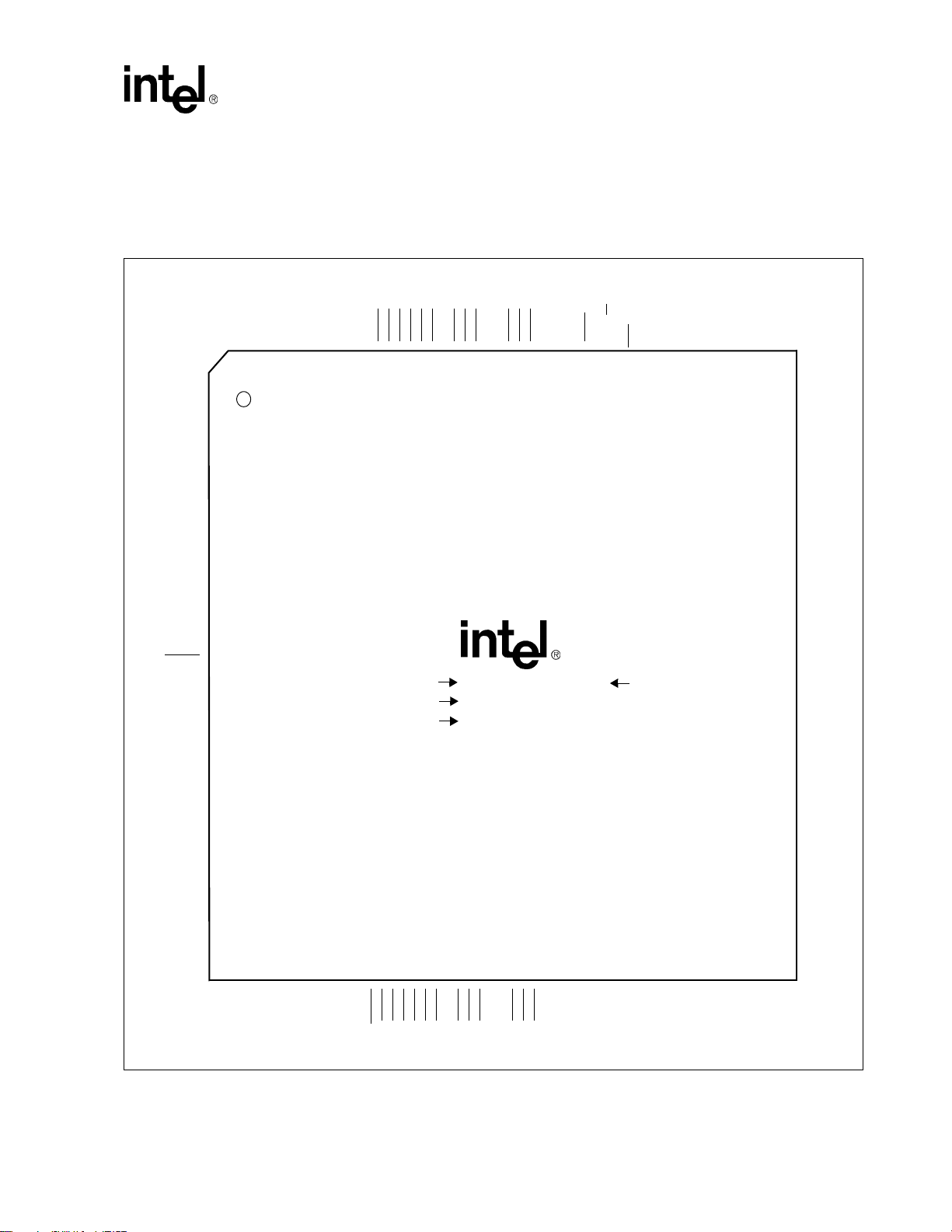
Intel® LXT9785 and Intel® LXT9785E Advanced 8-Port 10/100 Mbps PHY Transceivers
3.1.3 PQFP Pin Assignments – SS-SMII Configuration
Figure 4 and Table 4, “Intel® LXT9785/LXT9785 SS-SMII PQFP Pin List” on page 32 provide
the LXT9785/LXT9785E SS-SMII PQFP pin assignments.
Figure 4. Intel
N/CLINKHOLD ......2
N/C ......1
N/C ......3
TxData6 ......4
N/C ......5
REFCLK1 ......6
RxData5 ......7
N/C ......8
GNDIO ......9
N/C ......10
FIFOSEL1 ......11
N/C ......12
TxData5 ......13
N/C ......14
RxData4 ......15
N/C ......16
RxSYNC1 ......17
VCCIO ......18
GNDIO ......19
FIFOSEL0 ......20
RxCLK1 ......21
TxData4 ......22
N/C ......23
MDC1 ......24
MDIO1 ......25
MDINT1 ......26
RxData3 ......27
N/C ......28
VCCIO ......29
GNDIO ......30
N/C ......31
TxCLK0 ......32
N/C ......33
TxData3 ......34
TxSYNC0 ......35
RxData2 ......36
N/C ......37
GNDIO ......38
N/C ......39
PREASEL ......40
N/C ......41
TxData2 ......42
N/C ......43
REFCLK0 ......44
RxData1 ......45
N/C ......46
VCCIO ......47
GNDIO ......48
N/C ......49
PAUSE ......50
N/C ......51
TxData1 ......52
®
LXT9785/LXT9785E SS-SMII 208-Pin PQFP Assignments
208 ......... VCCIO
207 ......... GNDIO
206 ......... N/C
205 ......... RxData6
204 ......... TxSYNC1
203 ......... TxData7
202 ......... N/C
201 ......... TxCLK1
200 ......... N/C
199 ......... GNDIO
198 ......... N/C
197 ......... RxData7
196 .........VCCD
195 ......... GNDD
194 ......... LED7_3
193 ......... LED7_2
192 ......... LED7_1
191 ......... LED6_3
190 ......... LED6_2
189 ......... LED6_1
188 ......... GNDIO
187 ......... LED5_3
186 ......... LED5_2
185 ......... LED5_1
184 ......... VCCD
183 ......... GNDD
182 ......... LED4_3
181 ......... LED4_2
180 ......... LED4_1
179 ......... SGND
178 ......... ModeSel_1
177 ......... ModeSel_0
176 ......... Section
175 ......... RESET
174 ......... PWRDWN
Part #
LOT #
FPO #
LXT9785/9785E XX
XXXXXX
XXXXXXXX
173 ......... G_FX/TP
172 ......... N/C
Rev #
171....... TRST
170 ......... TCK
169 ......... TMS
168 ......... TDO
167 ......... TDI
166 ......... SD7
165 ......... SD6
164 ......... VCCPECL
163 ......... GNDPECL
162 ......... SD5
161 ......... SD4
160 ......... N/C
159 ......... N/C
158 ......... VCCR7
157 ......... TPFIP7
156......... TPFIN7
155......... GNDR7
154......... TPFOP7
153......... TPFON7
152......... VCCT6/7
151......... TPFON6
150......... TPFOP6
149......... GNDR6
148......... GNDT6/7
147......... TPFIN6
146......... TPFIP6
145......... VCCR6
144......... VCCR5
143......... TPFIP5
142......... TPFIN5
141......... GNDR5
140......... TPFOP5
139......... TPFON5
138......... VCCT4/5
137......... TPFON4
136......... TPFOP4
135......... GNDR4
134......... GNDT4/5
133......... TPFIN4
132......... TPFIP4
131......... VCCR4
130......... VCCR3
129......... TPFIP3
128......... TPFIN3
127......... GNDT2/3
126......... GNDR3
125......... TPFOP3
124......... TPFON3
123......... VCCT2/3
122......... TPFON2
121......... TPFOP2
120......... GNDR2
119......... TPFIN2
118......... TPFIP2
117......... VCCR2
116......... VCCR1
115......... TPFIP1
114......... TPFIN1
113......... GNDT0/1
112......... GNDR1
111......... TPFOP1
110......... TPFON1
109......... VCCT0/1
108......... TPFON0
107......... TPFOP0
106......... GNDR0
105......... TPFIN0
N/C...... 53
N/C...... 55
VCCIO...... 56
GNDIO...... 57
RxData0...... 54
N/C...... 62
MDIX...... 59
MDC0...... 63
VCCD...... 65
GNDD...... 66
MDIO0...... 64
LED3_3...... 68
LED3_2...... 69
LED3_1...... 70
LED2_3...... 71
LED2_2...... 72
TxData0...... 61
RxCLK0...... 60
RxSYNC0...... 58
MDINT0...... 67
LED2_1...... 73
VCCD...... 78
GNDIO...... 74
GNDD...... 79
LED1_3...... 75
LED1_2...... 76
LED1_1...... 77
LED0_3...... 80
CFG_3...... 85
CFG_2...... 86
CFG_1...... 87
ADD_4...... 88
ADD_3...... 89
ADD_2...... 90
MDDIS...... 84
LED0_2...... 81
LED0_1...... 82
AMDIX_EN...... 83
ADD_1...... 91
SD0...... 96
ADD_0...... 92
SD1...... 97
SD_2P5V...... 95
TxSlew_1...... 93
TxSlew_0...... 94
N/C...... 102
SD2...... 100
SD3...... 101
TPFIP0...... 104
VCCPECL...... 98
VCCR0...... 103
GNDPECL...... 99
Datasheet 31
Document Number: 249241
Revision Number: 007
Revision Date: August 28, 2003
Page 30
Intel® LXT9785 and Intel® LXT9785E Advanced 8-Port 10/100 Mbps PHY Transceivers
Table 4. Intel® LXT9785/LXT9785 SS-SMII PQFP Pin List
Pin Symbol Type
Reference for Full
1
Description
Pin Symbol Type
Reference for Full
1
Description
1N/C – Table 16 (page 50)
N/C
2
LINKHOLD
Table 13 (page 43)
3N/C – Table 16 (page 50)
4 TxData6 I, ID Table 6 (page 39)
5N/C I Table 16 (page 50)
6 REFCLK1 I Table 6 (page 39)
7 RxData5
O, TS,
ID
Table 8 (page 40)
8N/C – Table 16 (page 50)
9 GNDIO – Table 15 (page 48)
10 N/C – Table 16 (page 50)
11 FIFOSEL1 I, ID, ST Table 13 (page 43)
12 N/C – Table 16 (page 50)
13 TxData5 I, ID Table 6 (page 39)
14 N/C – Table 16 (page 50)
15 RxData4
O, TS,
ID
Table 8 (page 40)
16 N/C – Table 16 (page 50)
17 RxSYNC1
O, TS,
ID
Table 8 (page 40)
18 VCCIO – Table 15 (page 48)
19 GNDIO – Table 15 (page 48)
20 FIFOSEL0 I, ID, ST Table 13 (page 43)
21 RxCLK1
O, TS,
ID
Table 8 (page 40)
22 TxData4 I, ID Table 6 (page 39)
23 N/C – Table 16 (page 50)
24 MDC1 I, ST, ID Table 9 (page 41)
25 MDIO1
26 MDINT1
27 RxData3
I/O, TS,
SL, IP
OD, TS,
SL, IP
O, TS,
ID
Table 9 (page 41)
Table 9 (page 41)
Table 8 (page 40)
28 N/C – Table 16 (page 50)
29 VCCIO – Table 15 (page 48)
30 GNDIO – Table 15 (page 48)
31 N/C – Table 16 (page 50)
32 TxCLK0 I, ID Table 8 (page 40)
33 N/C – Table 16 (page 50)
34 TxData3 I, ID Table 6 (page 39)
35 TxSYNC0 I, ID Table 8 (page 40)
36 RxData2
O, TS,
ID
Table 8 (page 40)
37 N/C – Table 16 (page 50)
38 GNDIO – Table 15 (page 48)
39 N/C – Table 16 (page 50)
40 PREASEL I, ST Table 13 (page 43)
41 N/C – Table 16 (page 50)
42 TxData2 I, ID Table 6 (page 39)
43 N/C – Table 16 (page 50)
44 REFCLK0 I Table 6 (page 39)
45 RxData1
O, TS,
ID
Table 8 (page 40)
46 N/C – Table 16 (page 50)
47 VCCIO – Table 15 (page 48)
48 GNDIO – Table 15 (page 48)
49 N/C – Table 16 (page 50)
50 PAUSE I, ID, ST Table 13 (page 43)
51 N/C – Table 16 (page 50)
52 TxData1 I, ID Table 6 (page 39)
53 N/C – Table 16 (page 50)
54 RxData0
O, TS,
ID
Table 8 (page 40)
55 N/C – Table 16 (page 50)
56 VCCIO – Table 15 (page 48)
57 GNDIO – Table 15 (page 48)
58 RxSYNC0
O, TS,
ID
Table 8 (page 40)
59 MDIX I, ID, ST Table 13 (page 43)
60 RxCLK0 – Table 8 (page 40)
61 TxData0 I, ID Table 6 (page 39)
62 N/C – Table 16 (page 50)
63 MDC0 I, ST, ID Table 9 (page 41)
64 MDIO0
I/O, TS,
SL, IP
Table 9 (page 41)
65 VCCD – Table 15 (page 48)
66 GNDD – Table 15 (page 48)
32 Datasheet
Document Number: 249241
Revision Date: August 28, 2003
Revision Number: 007
Page 31

Intel® LXT9785 and Intel® LXT9785E Advanced 8-Port 10/100 Mbps PHY Transceivers
Reference for Full
Pin Symbol Type
67 MDINT0
68 LED3_3
69 LED3_2
70 LED3_1
71 LED2_3
72 LED2_2
73 LED2_1
1
OD, TS,
SL, IP
OD, TS,
SO, IP
OD, TS,
SL, IP
OD, TS,
SL, IP
OD, TS,
SL, IP
OD, TS,
SL, IP
OD, TS,
SL, IP
Description
Table 9 (page 41)
Table 14 (page 47)
Table 14 (page 47)
Table 14 (page 47)
Table 14 (page 47)
Table 14 (page 47)
Table 14 (page 47)
74 GNDIO – Table 15 (page 48)
75 LED1_3
76 LED1_2
77 LED1_1
OD, TS,
SL, IP
OD, TS,
SL, IP
OD, TS,
SL, IP
Table 14 (page 47)
Table 14 (page 47)
Table 14 (page 47)
78 VCCD – Table 15 (page 48)
79 GNDD – Table 15 (page 48)
80 LED0_3
81 LED0_2
82 LED0_1
OD, TS,
SL, IP
OD, TS,
SL, IP
OD, TS,
SL, IP
Table 14 (page 47)
Table 14 (page 47)
Table 14 (page 47)
83 AMDIX_EN I, ST, IP Table 13 (page 43)
84 MDDIS I, ST, ID Table 9 (page 41)
85 CFG_3 I, ST, ID Table 13 (page 43)
86 CFG_2 I, ST, ID Table 13 (page 43)
87 CFG_1 I, ST, ID Table 13 (page 43)
88 ADD_4 I, ST, ID Table 13 (page 43)
89 ADD_3 I, ST, ID Table 13 (page 43)
90 ADD_2 I, ST, ID Table 13 (page 43)
91 ADD_1 I, ST, ID Table 13 (page 43)
92 ADD_0 I, ST, ID Table 13 (page 43)
93 TxSLEW_1 I, ST, ID Table 13 (page 43)
94 TxSLEW_0 I, ST, ID Table 13 (page 43)
95 SD_2P5V I, ST, ID Table 10 (page 42)
96 SD0 I Table 10 (page 42)
Reference for Full
Pin Symbol Type
1
Description
97 SD1 I Table 10 (page 42)
98 VCCPECL – Table 15 (page 48)
99 GNDPECL – Table 15 (page 48)
100 SD2 I Table 10 (page 42)
101 SD3 I Table 10 (page 42)
102 N/C – Table 16 (page 50)
103 VCCR0 – Table 15 (page 48)
104 TPFIP0 AI/AO Table 11 (page 42)
105 TPFIN0 AI/AO Table 11 (page 42)
106 GNDR0 – Table 15 (page 48)
107 TPFOP0 AO/AI Table 11 (page 42)
108 TPFON0 AO/AI Table 11 (page 42)
109 VCCT0/1 – Table 15 (page 48)
110 TPFON1 AO/AI Table 11 (page 42)
111 TPFOP1 AO/AI Table 11 (page 42)
112 GNDR1 – Table 15 (page 48)
113 GNDT0/1 – Table 15 (page 48)
114 TPFIN1 AI/AO Table 11 (page 42)
115 TPFIP1 AI/AO Table 11 (page 42)
116 VCCR1 – Table 15 (page 48)
117 VCCR2 – Table 15 (page 48)
118 TPFIP2 AI/AO Table 11 (page 42)
119 TPFIN2 AI/AO Table 11 (page 42)
120 GNDR2 – Table 15 (page 48)
121 TPFOP2 AO/AI Table 11 (page 42)
122 TPFON2 AO/AI Table 11 (page 42)
123 VCCT2/3 – Table 15 (page 48)
124 TPFON3 AO/AI Table 11 (page 42)
125 TPFOP3 AO/AI Table 11 (page 42)
126 GNDR3 – Table 15 (page 48)
127 GNDT2/3 – Table 15 (page 48)
128 TPFIN3 AI/AO Table 11 (page 42)
129 TPFIP3 AI/AO Table 11 (page 42)
130 VCCR3 – Table 15 (page 48)
131 VCCR4 – Table 15 (page 48)
132 TPFIP4 AI/AO Table 11 (page 42)
133 TPFIN4 AI/AO Table 11 (page 42)
134 GNDT4/5 – Table 15 (page 48)
Datasheet 33
Document Number: 249241
Revision Number: 007
Revision Date: August 28, 2003
Page 32

Intel® LXT9785 and Intel® LXT9785E Advanced 8-Port 10/100 Mbps PHY Transceivers
Reference for Full
Pin Symbol Type
1
Description
135 GNDR4 – Table 15 (page 48)
136 TPFOP4 AO/AI Table 11 (page 42)
137 TPFON4 AO/AI Table 11 (page 42)
138 VCCT4/5 – Table 15 (page 48)
139 TPFON5 AO/AI Table 11 (page 42)
140 TPFOP5 AO/AI Table 11 (page 42)
141 GNDR5 – Table 15 (page 48)
142 TPFIN5 AI/AO Table 11 (page 42)
143 TPFIP5 AI/AO Table 11 (page 42)
144 VCCR5 – Table 15 (page 48)
145 VCCR6 – Table 15 (page 48)
146 TPFIP6 AI/AO Table 11 (page 42)
147 TPFIN6 AI/AO Table 11 (page 42)
148 GNDT6/7 – Table 15 (page 48)
149 GNDR6 – Table 15 (page 48)
150 TPFOP6 AO/AI Table 11 (page 42)
151 TPFON6 AO/AI Table 11 (page 42)
152 VCCT6/7 – Table 15 (page 48)
153 TPFON7 AO/AI Table 11 (page 42)
154 TPFOP7 AO/AI Table 11 (page 42)
155 GNDR7 – Table 15 (page 48)
156 TPFIN7 AI/AO Table 11 (page 42)
157 TPFIP7 AI/AO Table 11 (page 42)
158 VCCR7 – Table 15 (page 48)
159 N/C – Table 16 (page 50)
160 N/C – Table 16 (page 50)
161 SD4 I Table 10 (page 42)
162 SD5 I Table 10 (page 42)
163 GNDPECL – Table 15 (page 48)
164 VCCPECL – Table 15 (page 48)
165 SD6 I Table 10 (page 42)
166 SD7 I Table 10 (page 42)
167 TDI I, ST, IP Table 12 (page 43)
168 TDO O, TS Table 12 (page 43)
169 TMS I, ST, IP Table 12 (page 43)
170 TCK I, ST, ID Table 12 (page 43)
171 TRST
I, ST, IP Table 12 (page 43)
172 N/C – Table 16 (page 50)
Reference for Full
Pin Symbol Type
1
Description
173 G_FX/TP I, ST, ID Table 13 (page 43)
174 PWRDWN I, ST, ID Table 13 (page 43)
175 RESET
I, ST, IP Table 13 (page 43)
176 SECTION I, ST, ID Table 13 (page 43)
177 ModeSel0 I, ST, ID Table 13 (page 43)
178 ModeSel1 I, ST, ID Table 13 (page 43)
179 SGND – Table 15 (page 48)
180 LED4_1
181 LED4_2
182 LED4_3
OD, TS,
SL, IP
OD, TS,
SL, IP
OD, TS,
SL, IP
Table 14 (page 47)
Table 14 (page 47)
Table 14 (page 47)
183 GNDD – Table 15 (page 48)
184 VCCD – Table 15 (page 48)
185 LED5_1
186 LED5_2
187 LED5_3
OD, TS,
SL, IP
OD, TS,
SL, IP
OD, TS,
SL, IP
Table 14 (page 47)
Table 14 (page 47)
Table 14 (page 47)
188 GNDIO – Table 15 (page 48)
189 LED6_1
190 LED6_2
191 LED6_3
192 LED7_1
193 LED7_2
194 LED7_3
OD, TS,
SL, IP
OD, TS,
SL, IP
OD, TS,
SL, IP
OD, TS,
SL, IP
OD, TS,
SL, IP
OD, TS,
SL, IP
Table 14 (page 47)
Table 14 (page 47)
Table 14 (page 47)
Table 14 (page 47)
Table 14 (page 47)
Table 14 (page 47)
195 GNDD – Table 15 (page 48)
196 VCCD – Table 15 (page 48)
197 RxData7
O, TS,
ID
Table 8 (page 40)
198 N/C – Table 16 (page 50)
199 GNDIO – Table 15 (page 48)
200 N/C – Table 16 (page 50)
201 TxCLK1 I, ID Table 8 (page 40)
202 N/C – Table 16 (page 50)
34 Datasheet
Document Number: 249241
Revision Date: August 28, 2003
Revision Number: 007
Page 33

Intel® LXT9785 and Intel® LXT9785E Advanced 8-Port 10/100 Mbps PHY Transceivers
Reference for Full
Pin Symbol Type
203 TxData7 I, ID Table 6 (page 39)
204 TxSYNC1 I, ID Table 8 (page 40)
205 RxData6
206 N/C – Table 16 (page 50)
207 GNDIO – Table 15 (page 48)
208 VCCIO – Table 15 (page 48)
1
O, TS,
ID
Description
Table 8 (page 40)
Datasheet 35
Document Number: 249241
Revision Number: 007
Revision Date: August 28, 2003
Page 34

LXT9785 and LXT9785E Advanced 8-Port 10/100 Mbps PHY Transceivers
3.2 PQFP Signal Descriptions
3.2.1 Signal Name Conventions
Signal names may contain either a port designation or a serial designation, or a combination of the
two designations. Signal naming conventions are as follows:
• Port Number Only. Individual signals that apply to a particular port are designated by the
Signal Mnemonic, immediately followed by the Port Designation. For example, Transmit
Enable signals would be identified as TxEN0, TxEN1, and TxEN2.
• Serial Number Only. A set of signals which are not tied to any specific port are designated by
the Signal Mnemonic, followed by an underscore and a serial designation. For example, a set
of three Global Configuration signals would be identified as CFG_1, CFG_2, and CFG_3.
• Port and Serial Number. In cases where each port is assigned a set of multiple signals, each
signal is designated in the following order: Signal Mnemonic, Port Designation, an
underscore, and the serial designation. For example, a set of three Port Configuration signals
would be identified as RxData0_0 and RxData0_1, RxData1_0 and RxData1_1, and
RxData2_0 and RxData2_1.
3.2.2 PQFP Signal Descriptions – RMII, SMII, and SS-SMII Configurations
Table 5 through Table 17, “Intel® LXT9785/LXT9785E Receive FIFO Depth Considerations” on
page 50 provide PQFP signal descriptions. Ball designations are included for cross-reference.
Table 5. Intel
PQFP PBGA
1. Type Column Coding: I = Input, O = Output, OD = Open Drain output, ST = Schmitt Triggered input, TS =
2. The IP/ID resistors are disabled during H/W Power-Down mode. If a Pin is an output or an I/O, the IP/ID
3. RxData[0:7]_0, RxData[0:7]_1, CRS_DV[0:7] and RxER[0:7] outputs are three-stated in Isolation and H/W
®
LXT9785/LXT9785E RMII Signal Descriptions – PQFP (Sheet 1 of 3)
Pin-Ball
Designation
44
6
61
62
52
53
42
43
Three-State-able output, SL = Slew-rate Limited output, IP = weak Internal Pull-up, ID = weak Internal pullDown.
resistors are also disabled when the output is enabled.
Power-Down modes and during H/W reset.
E6,
E12
E2,
F4
C3,
D4
B5
A4
Symbol Type
REFCLK0
REFCLK1
TxData0_0
TxData0_1
TxData1_0
TxData1_1
TxData2_0
TxData2_1
I
I, ID
I, ID
I, ID
1
Signal Description
Reference Clock.
50 MHz RMII reference clock is always required. RMII
inputs are sampled on the rising edge of REFCLK,
RMII outputs are sourced on the falling edge. See
“Clock/SYNC Requirements” on page 125 for detailed
CLK requirements.
Transmit Data - Port 0.
Inputs containing 2-bit parallel di-bits to be transmitted
from port 0 are clocked in synchronously to REFCLK.
Transmit Data - Port 1.
Inputs containing 2-bit parallel di-bits to be transmitted
from port 1 are clocked in synchronously to REFCLK
Transmit Data - Port 2.
Inputs containing 2-bit parallel di-bits to be transmitted
from port 2 are clocked in synchronously to REFCLK.
2,3
36 Datasheet
Document Number: 249241
Revision Date: August 28, 2003
Revision Number: 007
Page 35

LXT9785 and LXT9785E Advanced 8-Port 10/100 Mbps PHY Transceivers
Table 5. Intel® LXT9785/LXT9785E RMII Signal Descriptions – PQFP (Sheet 2 of 3)
Pin-Ball
Designation
Symbol Type
PQFP PBGA
34
35
22
23
13
14
4
5
203
204
60
51
41
33
21
12
3
202
55
54
46
45
37
36
28
27
16
15
8
7
D8,
A6
A11,
C10
B13,
D11
D13,
A16
E14,
C16
E3,
B2,
C6,
A7,
B11,
A14,
C14,
D16
C2,
B1
A3,
B4
B6,
C7
D9,
B9
A13,
C12
B14,
B15
TxData3_0
TxData3_1
TxData4_0
TxData4_1
TxData5_0
TxData5_1
TxData6_0
TxData6_1
TxData7_0
TxData7_1
TxEN0
TxEN1
TxEN2
TxEN3
TxEN4
TxEN5
TxEN6
TxEN7
RxData0_0
RxData0_1
RxData1_0
RxData1_1
RxData2_0
RxData2_1
RxData3_0
RxData3_1
RxData4_0
RxData4_1
RxData5_0
RxData5_1
1. Type Column Coding: I = Input, O = Output, OD = Open Drain output, ST = Schmitt Triggered input, TS =
Three-State-able output, SL = Slew-rate Limited output, IP = weak Internal Pull-up, ID = weak Internal pullDown.
2. The IP/ID resistors are disabled during H/W Power-Down mode. If a Pin is an output or an I/O, the IP/ID
resistors are also disabled when the output is enabled.
3. RxData[0:7]_0, RxData[0:7]_1, CRS_DV[0:7] and RxER[0:7] outputs are three-stated in Isolation and H/W
Power-Down modes and during H/W reset.
1
I, ID
I, ID
I, ID
I, ID
I, ID
I, ID
O, TS
O, TS, ID
O, TS
O, TS, ID
O, TS
O, TS, ID
O, TS
O, TS, ID
O, TS
O, TS, ID
O, TS
O, TS, ID
Signal Description
2,3
Transmit Data - Port 3.
Inputs containing 2-bit parallel di-bits to be transmitted
from port 3 are clocked in synchronously to REFCLK.
Transmit Data - Port 4.
Inputs containing 2-bit parallel di-bits to be transmitted
from port 4 are clocked in synchronously to REFCLK.
Transmit Data - Port 5.
Inputs containing 2-bit parallel di-bits to be transmitted
from port 5 are clocked in synchronously to REFCLK.
Transmit Data - Port 6.
Inputs containing 2-bit parallel di-bits to be transmitted
from port 6 are clocked in synchronously to REFCLK.
Transmit Data - Port 7.
Inputs containing 2-bit parallel di-bits to be transmitted
from port 7 are clocked in synchronously to REFCLK.
Transmit Enable - Ports 0-7.
Active High input enables respective port transmitter.
This signal must be synchronous to the REFCLK.
Receive Data - Port 0.
Receive data signals (2-bit parallel di-bits) are driven
synchronously to REFCLK.
Receive Data - Port 1.
Receive data signals (2-bit parallel di-bits) are driven
synchronously to REFCLK.
Receive Data - Port 2.
Receive data signals (2-bit parallel di-bits) are driven
synchronously to REFCLK.
Receive Data - Port 3.
Receive data signals (2-bit parallel di-bits) are driven
synchronously to REFCLK.
Receive Data - Port 4.
Receive data signals (2-bit parallel di-bits) are driven
synchronously to REFCLK.
Receive Data - Port 5.
Receive data signals (2-bit parallel di-bits) are driven
synchronously to REFCLK.
Datasheet 37
Document Number: 249241
Revision Number: 007
Revision Date: August 28, 2003
Page 36

LXT9785 and LXT9785E Advanced 8-Port 10/100 Mbps PHY Transceivers
Table 5. Intel® LXT9785/LXT9785E RMII Signal Descriptions – PQFP (Sheet 3 of 3)
Pin-Ball
Designation
Symbol Type
PQFP PBGA
206
205
198
197
58
49
39
31
17
10
1
200
59
50
40
32
20
11
2
201
C15,
B17
E16,
F14
E4,
C4,
A5,
B8,
B12,
D12,
B16,
E15
D2,
D5,
D7,
C8,
A12,
A15,
A17,
D17
RxData6_0
RxData6_1
RxData7_0
RxData7_1
CRS_DV0
CRS_DV1
CRS_DV2
CRS_DV3
CRS_DV4
CRS_DV5
CRS_DV6
CRS_DV7
RxER0
RxER1
RxER2
RxER3
RxER4
RxER5
RxER6
RxER7
1. Type Column Coding: I = Input, O = Output, OD = Open Drain output, ST = Schmitt Triggered input, TS =
Three-State-able output, SL = Slew-rate Limited output, IP = weak Internal Pull-up, ID = weak Internal pullDown.
2. The IP/ID resistors are disabled during H/W Power-Down mode. If a Pin is an output or an I/O, the IP/ID
resistors are also disabled when the output is enabled.
3. RxData[0:7]_0, RxData[0:7]_1, CRS_DV[0:7] and RxER[0:7] outputs are three-stated in Isolation and H/W
Power-Down modes and during H/W reset.
1
O, TS
O, TS, ID
O, TS
O, TS, ID
O, TS, SL,
ID
O, TS, SL,
ID
Signal Description
2,3
Receive Data - Port 6.
Receive data signals (2-bit parallel di-bits) are driven
synchronously to REFCLK.
Receive Data - Port 7.
Receive data signals (2-bit parallel di-bits) are driven
synchronously to REFCLK.
Carrier Sense/Receive Data Valid - Ports 0-7.
On detection of valid carrier, these signals are
asserted asynchronously with respect to REFCLK.
CRS_DVn is de-asserted on loss of carrier,
synchronous to REFCLK.
Receive Error - Ports 0-7.
These signals are synchronous to the respective
REFCLK. Active High indicates that received code
group is invalid, or that PLL is not locked.
The RxER signals have the following additional
function pins:
RxER0 (MDIX)
RxER1 (PAUSE)
RxER2 (PREASEL)
RxER4 (FIFOSEL0)
RxER5 (FIFOSEL1)
RxER6 (LINKHOLD)
38 Datasheet
Document Number: 249241
Revision Date: August 28, 2003
Revision Number: 007
Page 37
LXT9785 and LXT9785E Advanced 8-Port 10/100 Mbps PHY Transceivers
Table 6. Intel® LXT9785/LXT9785E SMII / SS-SMII Common Signal Descriptions – PQFP
Pin/Ball
Designation
Symbol Type
PQFP PBGA
61
52
42
34
22
13
4
203
44
6
E2,
C3,
B5,
D8,
A11,
B13,
D13,
E14
E6,
E12
TxData0
TxData1
TxData2
TxData3
TxData4
TxData5
TxData6
TxData7
REFCLK0
REFCLK1
1. Type Column Coding: I = Input, O = Output, OD = Open Drain output, ST = Schmitt Triggered input, TS =
Three-State-able output, SL = Slew-rate Limited output, IP = weak Internal Pull-up, ID = weak Internal pullDown.
2. The IP/ID resistors are disabled during H/W Power-Down mode.
I, ID
I
1
Signal Description
2
Transmit Data - Ports 0-7.
These serial input streams provide data to be transmitted to
the network. The LXT9785/9785E clocks the data in
synchronously to REFCLK.
Reference Clock.
The LXT9785/9785E always requires a 125 MHz reference
clock input. Refer to Functional Description for detailed clock
requirements. REFCLK0 and REFCLK1 are always
connected regardless of sectionalization mode.
Table 7. Intel® LXT9785/LXT9785E SMII Specific Signal Descriptions – PQFP
Pin/Ball
Designation
Symbol Type
PQFP PBGA
35
204
55
46
37
28
16
8
206
198
A6,
C16
C2,
A3,
B6,
D9,
A13,
B14,
C15,
E16
SYNC0
SYNC1
RxData0
RxData1
RxData2
RxData3
RxData4
RxData5
RxData6
RxData7
1. Type Column Coding: I = Input, O = Output, OD = Open Drain output, ST = Schmitt Triggered input, TS =
Three-State-able output, SL = Slew-rate Limited output, IP = weak Internal Pull-up, ID = weak Internal pullDown.
2. The IP/ID resistors are disabled during H/W Power-Down mode.
3. RxData[0:7] outputs are three-stated in Isolation and hardware power-down modes and during hardware
reset.
I, ID
O, TS
1
Signal Description
SMII Synchronization.
The MAC must generate a SYNC pulse every 10 REFCLK
cycles to synchronize the SMII. SYNC0 is used when 1x8
port sectionalization is selected. SYNC0 and SYNC1 are
to be used when 2x4 port sectionalization is chosen.
Receive Data - Ports 0-7.
These serial output streams provide data received from
the network. The LXT9785/9785E drives the data out
synchronously to REFCLK.
2,3
Datasheet 39
Document Number: 249241
Revision Number: 007
Revision Date: August 28, 2003
Page 38

LXT9785 and LXT9785E Advanced 8-Port 10/100 Mbps PHY Transceivers
Table 8. Intel® LXT9785/LXT9785E SS-SMII Specific Signal Descriptions – PQFP
Pin/Ball
Designation
Symbol Type
PQFP PBGA
35
204
58
17
32
201
60
21
54
45
36
27
15
7
205
197
A6,
C16
E4,
B12
C8,
D17
E3,
B11
B1,
B4,
C7,
B9,
C12,
B15,
B17,
F14
TxSYNC0
TxSYNC1
RxSYNC0
RxSYNC1
TxCLK0
TxCLK1
RxCLK0
RxCLK1
RxData0
RxData1
RxData2
RxData3
RxData4
RxData5
RxData6
RxData7
1. Type Column Coding: I = Input, O = Output, OD = Open Drain output, ST = Schmitt Triggered input, TS =
Three-State-able output, SL = Slew-rate Limited output, IP = weak Internal Pull-up, ID = weak Internal pullDown.
2. The IP/ID resistors are disabled during H/W Power-Down mode. If a Pin is an output or an I/O, the IP/ID
resistors are also disabled when the output is enabled.
3. RxData[0:7], RxSYNC[0:1], and RxCLK[0:1] outputs are three-stated in Isolation and H/W Power-Down
modes and during H/W reset.
I, ID
O, TS,
ID
I, ID
O, TS,
ID
O, TS,
ID
1
Signal Description
2,3
SS-SMII Transmit Synchronization.
The MAC must generate a TxSYNC pulse every 10 TxCLK
cycles to mark the start of TxData segments. TxSYNC0 is
used when 1x8 port sectionalization is selected.
SS-SMII Receive Synchronization.
The LXT9785/9785E generates these pulses every 10
RxCLK cycles to mark the start of RxData segments for the
MAC. RxSYNC1 is used when 1x8 port sectionalization is
selected. RxSYNC0 may not be used. These outputs are
only enabled when SS-SMII mode is enabled.
SS-SMII Transmit Clock.
The MAC sources this 125 MHz clock as the timing
reference for TxData and TxSYNC. Only TxCLK0 is used
when 1x8 port sectionalization is selected. See “Clock/
SYNC Requirements” on page 125 for detailed clock
requirements.
SS-SMII Receive Clock.
The LXT9785/9785E generates these clocks, based on
REFCLK, to provide a timing reference for RxData and
RxSYNC to the MAC. RxCLK1 is used when 1x8 port
sectionalization is selected. RxCLK0 may not be used. See
“Clock/SYNC Requirements” on page 125 for detailed clock
requirements. These outputs are only enabled when SSSMII mode is enabled.
Receive Data - Ports 0-7.
These serial output streams provide data received from
the network. The LXT9785/9785E drives the data out
synchronously to REFCLK.
40 Datasheet
Document Number: 249241
Revision Date: August 28, 2003
Revision Number: 007
Page 39

LXT9785 and LXT9785E Advanced 8-Port 10/100 Mbps PHY Transceivers
Table 9. Intel® LXT9785/LXT9785E MDIO Control Interface Signals – PQFP
Pin/Ball
Designation
Symbol Type
PQFP PBGA
64
25
67
26
63
24
F3,
A10
F1,
C9
E1,
B10
MDIO0
MDIO1
MDINT0
MDINT1
MDC0
MDC1
84 L1 MDDIS I, ST, ID
1. Type Column Coding: I = Input, O = Output, OD = Open Drain output, ST = Schmitt Triggered input, TS =
Three-State-able output, SL = Slew-rate Limited output, IP = weak Internal Pull-up, ID = weak Internal pullDown.
2. The IP/ID resistors are disabled during H/W Power-Down mode. If a Pin is an output or an I/O, the IP/ID
resistors are also disabled when the output is enabled.
3. MDIO[0:1] and MDINT
[0:1] outputs are three-stated in H/W Power-Down mode and during H/W reset.
4. Supports the 802.3 MDIO register set. Specific bits in the registers are referenced using an “X.Y” notation,
where X is the register number (0-32) and Y is the bit number (0-15).
1
I/O, TS, SL,
IP
OD,TS, SL,
IP
I, ST, ID
Signal Description
2,3,4
Management Data Input/Output.
Bidirectional serial data channel for communication
between the PHY and MAC or switch ASIC. Only
MDIO0 is used when 1x8 port sectionalization is
selected. In 2x4 port sectionalization mode, MDIO0
accesses ports 0-3 and MDIO1 accesses ports 4-7.
Refer to Figure 21 on page 140.
Management Data Interrupt.
When Register bit 18.1 = 1, an active Low output on this
Pin indicates status change. Only MDINT0
1x8 port sectionalization is selected. In 2x4 port
sectionalization mode, MDINT0
0-3 and MDINT1
is associated with ports 4-7. Refer to
Figure 21 on page 140.
Management Data Clock.
Clock for the MDIO serial data channel. Maximum
frequency is 20 MHz. Only MDC0 is used when 1x8 port
sectionalization is selected. In 2x4 port
sectionalization mode, MDC0 clocks ports 0-3 register
accesses and MDC1 clocks ports 4-7 register accesses.
Refer to Figure 21 on page 140.
Management Disable.
When MDDIS is tied High, the MDIO port is completely
disabled and the Hardware Control Interface pins set
their respective bits at power up and reset.
When MDDIS is pulled Low at power up or reset, via the
internal pull-down resistor or by tieing it to ground, the
Hardware Control Interface Pins control only the initial
or “default” values of their respective register bits. After
the power-up/reset cycle is complete, bit control reverts
to the MDIO serial channel.
is used when
is associated with ports
Datasheet 41
Document Number: 249241
Revision Number: 007
Revision Date: August 28, 2003
Page 40

LXT9785 and LXT9785E Advanced 8-Port 10/100 Mbps PHY Transceivers
Table 10. Intel® LXT9785/LXT9785E Signal Detect – PQFP
Pin/Ball
Designation
Symbol Type
PQFP PBGA
95 P1 SD_2P5V I, ST, ID
96
97
100
101
161
162
165
166
P2,
N4,
P3,
N5,
P15,
P16,
P17,
N17
SD0
SD1
SD2
SD3
SD4
SD5
SD6
SD7
1. Type Column Coding: I = Input, O = Output, OD = Open Drain output, ST = Schmitt Triggered input, TS =
Three-State-able output, SL = Slew-rate Limited output, IP = weak Internal Pull-up, ID = weak Internal pullDown.
2. The IP/ID resistors are disabled during H/W Power-Down mode.
3. Tie SD[0:7] inputs to GNDPECL if unused.
1
Signal Description
2,3
Signal Detect 2.5 Volt Interface.
SD input threshold voltage select.
Tie to VCCPECL = Select 2.5 V LVPECL input levels
Float or Tie to GNDPECL = Select 3.3 V LVPECL input
levels
Signal Detect - Ports 0-7.
Signal Detect input from the fiber transceiver (these inputs
are only active for ports operating in fiber mode).
I
Logic High = Normal operation (the process of searching
for receive idles for the purpose of bringing link up is
initiated)
Logic Low = Link is declared lost
Table 11. Intel® LXT9785/LXT9785E Network Interface Signal Descriptions – PQFP
Pin/Ball Designation
Symbol Type
PQFP PBGA
107, 108
111, 110
121, 122
125, 124
136, 137
140, 139
150, 151
154, 153
104, 105
115, 114
118, 119
129, 128
132, 133
143, 142
146, 147
157, 156
T2, U1,
T3, R4,
T6, U5,
U7, T7,
T10, R10,
T11, U11,
T14,U15,
R14, T15
R2, T1,
U3, T4,
R6, T5,
T8, R8,
T9, U9,
U13, T12,
R12, T13,
R16, T16
TPFOP0, TPFON0
TPFOP1, TPFON1
TPFOP2, TPFON2
TPFOP3, TPFON3
TPFOP4, TPFON4
TPFOP5, TPFON5
TPFOP6, TPFON6
TPFOP7, TPFON7
TPFIP0, TPFIN0
TPFIP1, TPFIN1
TPFIP2, TPFIN2
TPFIP3, TPFIN3
TPFIP4, TPFIN4
TPFIP5, TPFIN5
TPFIP6, TPFIN6
TPFIP7, TPFIN7
1. Type Column Coding: AI = Analog Input, AO = Analog Output.
2. Switched to Inputs (see TPFIP/N description) when not in fiber mode and MDIX is not active [that is,
twisted-pair, non-crossover MDI mode].
3. Switched to Outputs (see TPFOP/N description) when not in fiber mode and MDIX is not active [that is,
twisted-pair, non-crossover MDI mode].
AO/AI
AI/AO
1
Signal Description
Twisted-Pair/Fiber Outputs
2
, Positive &
Negative, Ports 0-7.
During 100BASE-TX or 10BASE-T operation,
TPFO pins drive 802.3 compliant pulses onto
the line.
During 100BASE-FX operation, TPFO pins
produce differential LVPECL outputs for fiber
transceivers.
Twisted-Pair/Fiber Inputs
3
, Positive &
Negative, Ports 0-7.
During 100BASE-TX or 10BASE-T operation,
TPFI pins receive differential 100BASE-TX or
10BASE-T signals from the line.
During 100BASE-FX operation, TPFI pins
receive differential LVPECL inputs from fiber
transceivers.
42 Datasheet
Document Number: 249241
Revision Date: August 28, 2003
Revision Number: 007
Page 41

LXT9785 and LXT9785E Advanced 8-Port 10/100 Mbps PHY Transceivers
Table 12. Intel® LXT9785/LXT9785E JTAG Test Signal Descriptions – PQFP
Pin/Ball
Designation
Symbol Type
PQFP PBGA
167 N14 TDI I, ST, IP
168 N15 TDO O, TS
169 N16 TMS I, ST, IP Test Mode Select.
170 M16 TCK I, ST, ID
171 M17 TRST
1. Type Column Coding: I = Input, O = Output, OD = Open Drain, TS = Three-State-able output, SMT =
Schmitt Triggered input, SL = Slew-rate Limited output, IP = weak Internal Pull-up, ID = weak Internal pullDown.
2. The IP/ID resistors are disabled during H/W Power-Down mode. If a pin is an output or an I/O, the IP/ID
resistors are also disabled when the output is enabled.
3. TDO output is three-stated in H/W Power-Down mode and during H/W reset.
I, ST, IP
1
Signal Description
2,3
Test Data Input.
Test data sampled with respect to the rising edge of TCK.
Test Data Output.
Test data driven with respect to the falling edge of TCK.
Test Clock.
Clock input for JTAG test.
Test Reset.
Reset input for JTAG test.
Table 13. Intel® LXT9785/LXT9785E Miscellaneous Signal Descriptions – PQFP (Sheet 1 of 4)
Pin/Ball
Designation
Symbol Type
PQFP PBGA
94
93
N3,
M4
TxSLEW_0
TxSLEW_1
1. Type Column Coding: I = Input, O = Output, OD = Open Drain Output, ST = Schmitt Triggered Input, TS =
Three-State-able Output, SL = Slew-rate Limited Output, IP = Weak Internal Pull-Up, ID = Weak Internal
Pull-Down.
2. The IP/ID resistors are disabled during hardware power-down mode.
I, ST, ID
1
Signal Description
2
Tx Output Slew Controls 0 and 1 Defaults.
These pins are read at startup or reset. Their value at
that time is used to set the default state of Register bits
27.11:10 for all ports. These register bits can be read
and overwritten after startup / reset.
These pins select the TX output slew rate for all ports
(rise and fall time) as follows:
TxSLEW_1 TxSLEW_0
Slew Rate (Rise and Fall
Time)
0 0 3.3 ns
0 1 3.6 ns
1 0 3.9 ns
1 1 4.2 ns
Datasheet 43
Document Number: 249241
Revision Number: 007
Revision Date: August 28, 2003
Page 42

LXT9785 and LXT9785E Advanced 8-Port 10/100 Mbps PHY Transceivers
Table 13. Intel® LXT9785/LXT9785E Miscellaneous Signal Descriptions – PQFP (Sheet 2 of 4)
Pin/Ball
Designation
Symbol Type
PQFP PBGA
50 D5 PAUSE I, ID, ST
174 L14 PWRDWN I, ST, ID
175 M15 RESET
88
89
90
91
92
178
177
L4,
M2,
M3,
N1,
N2
L17,
L16
ADD_4
ADD_3
ADD_2
ADD_1
ADD_0
MODESEL_1
MODESEL_0
176 L15 SECTION I, ST, ID
1. Type Column Coding: I = Input, O = Output, OD = Open Drain Output, ST = Schmitt Triggered Input, TS =
Three-State-able Output, SL = Slew-rate Limited Output, IP = Weak Internal Pull-Up, ID = Weak Internal
Pull-Down.
2. The IP/ID resistors are disabled during hardware power-down mode.
I, ST, IP
I, ST, ID
I, ST, ID
1
Signal Description
2
Pause Default.
This pin is read at startup or reset. Its value at that time
is used to set the default state of Register bit 4.10 for
all ports. This register bit can be read and overwritten
after startup / reset.
When High, the LXT9785/9785E advertises Pause
capabilities on all ports during auto-negotiation.
This pin is shared with RMII-RxER1. An external pullup resistor (see applications section for value) can be
used to set Pause active while RxER1 is three-stated
during H/W reset. If no pull-up is used, the default
Pause state is set inactive via the internal pull-down
resistor.
Power-Down.
When High, forces the LXT9785/9785E into global
power-down mode.
Pin is not on JTAG chain.
Reset.
This active low input is ORed with the control register
Reset Register bit 0.15. When held Low, all outputs are
forced to inactive state.
Pin is not on JTAG chain.
Address <4:0>.
Sets base address. Each port adds its port number
(starting with 0) to this address to determine its PHY
address.
Port 0 Address = Base
Port 1 Address = Base + 1
Port 2 Address = Base + 2
Port 3 Address = Base + 3
Port 4 Address = Base + 4
Port 5 Address = Base + 5
Port 6 Address = Base + 6
Port 7 Address = Base + 7
Mode Select[1:0].
00 = RMII
01 = SMII
10 = SS-SMII
11 = Reserved
All ports are configured the same. Interfaces cannot be
mixed and must be all RMII, SMII, or SS-SMII.
Sectionalization Select.
This pin selects sectionalization into separate ports.
0 = 1x8 ports,
1 = 2x4 ports
44 Datasheet
Document Number: 249241
Revision Date: August 28, 2003
Revision Number: 007
Page 43

LXT9785 and LXT9785E Advanced 8-Port 10/100 Mbps PHY Transceivers
Table 13. Intel® LXT9785/LXT9785E Miscellaneous Signal Descriptions – PQFP (Sheet 3 of 4)
Pin/Ball
Designation
Symbol Type
PQFP PBGA
83 K1 AMDIX_EN I, ST, IP
59 D2 MDIX I, ID, ST
85
86
87
L2,
L3,
M1
CFG_3
CFG_2
CFG_1
173 M14 G_FX/TP
1. Type Column Coding: I = Input, O = Output, OD = Open Drain Output, ST = Schmitt Triggered Input, TS =
Three-State-able Output, SL = Slew-rate Limited Output, IP = Weak Internal Pull-Up, ID = Weak Internal
Pull-Down.
2. The IP/ID resistors are disabled during hardware power-down mode.
I, ST, ID
I, ST, ID
1
Signal Description
2
Auto MDIX Enable Default.
This pin is read at startup or reset. Its value at that time
is used to set the default state of Register bit 27.9 for
all ports. These register bits can be read and
overwritten after startup / reset. Refer to Table 40 on
page 119.
When active (High), automatic MDI crossover (MDIX)
(regardless of segmentation) is selected for all ports.
When inactive (Low) MDIX is selected according to the
MDIX pin.
MDIX Select Default.
This pin is read at startup or reset. Its value at that time
is used to set the default state of Register bit 27.8 for
all ports. These register bits can be read and
overwritten after startup / reset. Refer to Table 40,
“Intel® LXT9785/LXT9785E MDIX Selection” on
page 119.
When AMDIX_EN is active this pin is ignored.
When AMDIX_EN is inactive, all ports are forced to the
MDI or the MDIX function regardless of segmentation.
If this pin is active (high), MDI crossover (MDIX) is
selected. If this pin is inactive, non-crossover MDI
mode is set.
This pin is shared with RMII-RxER0. An external pullup resistor (see applications section for value) can be
used to set MDIX active while RxER0 is three-stated
during H/W reset. If no pull-up is used, the default
MDIX state is set inactive via the internal pull-down
resistor. Do not tie this pin directly to VCCIO (vs. using
a pull-up) in non-RMII modes.
Global Port Configuration Defaults 1-3.
These pins are read at startup or reset. Their value at
that time is used to set the default state of register bits
shown in Table 42, “Intel® LXT9785/9785E Global
Hardware Configuration Settings” on page 129 for all
ports. These register bits can be read and overwritten
after startup / reset.
When operating in Hardware Control Mode, these pins
provide configuration control options for all the ports
(refer to page 129 for details).
Global FX/TP
Enable Default.
This pin is read at startup or reset. Its value at that time
is used to set the default state of Register bit 16.0 for
all ports. These register bits can be read and
overwritten after startup / reset. Refer to Table 92, “Port
Configuration Register (Address 16, Hex 10)” on page 207.
This input selects whether all the ports are defaulted to
TP vs. FX mode.
Datasheet 45
Document Number: 249241
Revision Number: 007
Revision Date: August 28, 2003
Page 44

LXT9785 and LXT9785E Advanced 8-Port 10/100 Mbps PHY Transceivers
Table 13. Intel® LXT9785/LXT9785E Miscellaneous Signal Descriptions – PQFP (Sheet 4 of 4)
Pin/Ball
Designation
Symbol Type
PQFP PBGA
11
20
A15
A12
FIFOSEL1
FIFOSEL0
40 D7 PREASEL I, ID, ST
I, ID, ST
1
Signal Description
2
FIFO Select <1:0>.
These pins are read at startup or reset. Their value at
that time is used to set the default state of Register bits
18.15:14 for all ports. These register bits can be read
and overwritten after startup/reset.
These pins are shared with RMII-RxER<5:4>. An
external pull-up resistor (see applications section for
value) can be used to set FIFO Select<1:0> to active
while RxER<5:4> are three-stated during hardware
reset. If no pull-up is used, the default FIFO select
state is set via the internal pull-down resistors.
See Table 17, “Intel® LXT9785/LXT9785E Receive
FIFO Depth Considerations” on page 50.
Preamble Select.
This pin is read at startup or reset. Its value at that time
is used to set the default state of Register bit 16.5 for
all ports. This register bit can be read and overwritten
after startup/reset.
This pin is shared with RMII-RxER2. An external pullup resistor (see applications section for value) can be
used to set Preamble Select to active while RxER2 is
three-stated during hardware reset. If no pull-up is
used, the default Preamble Select state is set via the
internal pull-down resistors.
Note: Preamble select has no effect in 100 Mbps
operation.
LINKHOLD Default. This pin is read at startup or
reset. Its value at that time is used to set the default
state of Register bit 0.11 for all ports. This register bit
can be read and overwritten after startup / reset. When
2 A17 LINKHOLD ID
High, the LXT9785/9785E powers down all ports.
This pin is shared with RMII-RxER6. An external pullup resistor (see applications section for value) can be
used to set LINKHOLD active while RxER6 is tri-stated
during H/W reset. If no pull-up is used, the default
LINKHOLD state is set inactive via the internal pulldown resistor.
1. Type Column Coding: I = Input, O = Output, OD = Open Drain Output, ST = Schmitt Triggered Input, TS =
Three-State-able Output, SL = Slew-rate Limited Output, IP = Weak Internal Pull-Up, ID = Weak Internal
Pull-Down.
2. The IP/ID resistors are disabled during hardware power-down mode.
46 Datasheet
Document Number: 249241
Revision Date: August 28, 2003
Revision Number: 007
Page 45

LXT9785 and LXT9785E Advanced 8-Port 10/100 Mbps PHY Transceivers
Table 14. Intel® LXT9785/LXT9785E LED Signal Descriptions – PQFP (Sheet 1 of 2)
Pin/Ball
Designation
Symbol Type
PQFP PBGA
82
81
80
77
76
75
73
72
71
70
69
68
180
181
182
K3,
K2,
J1
J4,
J3,
H1
H2,
H3,
G1
F2,
G3,
G4
K16,
K17,
J17
LED0_1
LED0_2
LED0_3
LED1_1
LED1_2
LED1_3
LED2_1
LED2_2
LED2_3
LED3_1
LED3_2
LED3_3
LED4_1
LED4_2
LED4_3
1. Type Column Coding: I = Input, O = Output, OD = Open Drain output, ST = Schmitt Triggered input, TS =
Three-State-able output, SL = Slew-rate Limited output, IP = weak Internal Pull-up, ID = weak Internal pullDown.
2. The IP/ID resistors are disabled during H/W Power-Down mode. If a pin is an output or an I/O, the IP/ID
resistors are also disabled when the output is enabled.
3. The LED outputs are three-stated in H/W Power-Down mode and during H/W reset.
4.
1
OD, TS, SL,
IP
OD, TS, SL,
IP
OD, TS, SL,
IP
OD, TS, SL,
IP
OD, TS, SL,
IP
Signal Description
2,3
Port 0 LED Drivers 1-3.
These pins drive LED indicators for Port 0. Each LED
can display one of several available status conditions
as selected by the LED Configuration Register (refer
to Table 96, “LED Configuration Register (Address
20, Hex 14)” on page 213 for details).
Port 1 LED Drivers 1-3.
These pins drive LED indicators for Port 1. Each LED
can display one of several available status conditions
as selected by the LED Configuration Register (refer
to Table 96, “LED Configuration Register (Address
20, Hex 14)” on page 213 for details).
Port 2 LED Drivers 1-3.
These pins drive LED indicators for Port 2. Each LED
can display one of several available status conditions
as selected by the LED Configuration Register (refer
to Table 96, “LED Configuration Register (Address
20, Hex 14)” on page 213 for details).
Port 3 LED Drivers 1-3.
These pins drive LED indicators for Port 3. Each LED
can display one of several available status conditions
as selected by the LED Configuration Register (refer
to Table 96, “LED Configuration Register (Address
20, Hex 14)” on page 213 for details).
Port 4 LED Drivers 1-3.
These pins drive LED indicators for Port 4. Each LED
can display one of several available status conditions
as selected by the LED Configuration Register (refer
to Table 96, “LED Configuration Register (Address
20, Hex 14)” on page 213 for details).
Datasheet 47
Document Number: 249241
Revision Number: 007
Revision Date: August 28, 2003
Page 46

LXT9785 and LXT9785E Advanced 8-Port 10/100 Mbps PHY Transceivers
Table 14. Intel® LXT9785/LXT9785E LED Signal Descriptions – PQFP (Sheet 2 of 2)
Pin/Ball
Designation
PQFP PBGA
185
186
187
189
190
191
192
193
194
1. Type Column Coding: I = Input, O = Output, OD = Open Drain output, ST = Schmitt Triggered input, TS =
Three-State-able output, SL = Slew-rate Limited output, IP = weak Internal Pull-up, ID = weak Internal pullDown.
2. The IP/ID resistors are disabled during H/W Power-Down mode. If a pin is an output or an I/O, the IP/ID
resistors are also disabled when the output is enabled.
3. The LED outputs are three-stated in H/W Power-Down mode and during H/W reset.
4.
J15,
J16,
H17
H15,
H16,
G17
G15,
F17,
F16
Symbol Type
LED5_1
LED5_2
LED5_3
LED6_1
LED6_2
LED6_3
LED7_1
LED7_2
LED7_3
1
OD, TS, SL,
IP
OD, TS, SL,
IP
OD, TS, SL,
IP
Signal Description
Port 5 LED Drivers 1-3.
These pins drive LED indicators for Port 5. Each LED
can display one of several available status conditions
as selected by the LED Configuration Register (refer
to Table 96, “LED Configuration Register (Address
20, Hex 14)” on page 213 for details).
Port 6 LED Drivers 1-3.
These pins drive LED indicators for Port 6. Each LED
can display one of several available status conditions
as selected by the LED Configuration Register (refer
to Table 96, “LED Configuration Register (Address
20, Hex 14)” on page 213 for details).
Port 7 LED Drivers 1-3.
These pins drive LED indicators for Port 7. Each LED
can display one of several available status conditions
as selected by the LED Configuration Register (refer
to Table 96, “LED Configuration Register (Address
20, Hex 14)” on page 213 for details).
2,3
Table 15. Intel® LXT9785/LXT9785E Power Supply Signal Descriptions – PQFP (Sheet 1 of 2)
Pin/Ball Designation
PQFP PBGA
65, 78, 184,
196
18, 29, 47,
56, 208
98, 164 L13, L5 VCCPECL -
103, 116,
117, 130,
131, 144,
145, 158
1. Type Column Coding: I = Input, O = Output, OD = Open Drain output, ST = Schmitt Triggered input, TS =
Three-State-able output, SL = Slew-rate Limited output, IP = weak Internal Pull-up, ID = weak Internal pullDown.
G13, J14,
F5, J5
A2, A8,
C1, C11,
D14
N13, P4,
P7, P8,
P9, P10,
P11, P12
Symbol Type Signal Description
VCCD -
VCCIO -
VCCR -
Digital Power Supply - Core.
+2.5 V supply for core digital circuits.
Digital Power Supply - I/O Ring.
+2.5/3.3 V supply for digital I/O circuits. The digital
input circuits running off of this rail, having a TTL-level
threshold and over-voltage protection, may be
interfaced with 3.3/5.0 V, when the IO supply is 3.3 V,
and 2.5/3.3/5.0 V when 2.5 V.
Digital Power Supply - PECL Signal Detect Inputs.
+2.5/3.3 V supply for PECL Signal Detect input
circuits. If Fiber Mode is not used, tie these pins to
GNDPECL to save power.
Analog Power Supply - Receive.
+2.5 V supply for all analog receive circuits.
48 Datasheet
Document Number: 249241
Revision Date: August 28, 2003
Revision Number: 007
Page 47

LXT9785 and LXT9785E Advanced 8-Port 10/100 Mbps PHY Transceivers
Table 15. Intel® LXT9785/LXT9785E Power Supply Signal Descriptions – PQFP (Sheet 2 of 2)
Pin/Ball Designation
PQFP PBGA
109, 123,
138, 152
66, 79,
183, 195
9, 19, 30,
38, 48, 57,
74, 188,
199, 207
99, 163 M5, M13 GNDPECL -
106, 112,
120, 126,
135, 141,
149, 155
113, 127,
134, 148
179 K14 SGND -
1. Type Column Coding: I = Input, O = Output, OD = Open Drain output, ST = Schmitt Triggered input, TS =
Three-State-able output, SL = Slew-rate Limited output, IP = weak Internal Pull-up, ID = weak Internal pullDown.
N6, N7,
N9, N11,
N12
A1, A9,
B3, B7,
C5, C13,
C17, D1,
D3, D6,
D10, D15,
E5, E7,
E9, E11,
E13, E17,
F13, H8,
H9, H10,
J8, J9,
J10, K8,
K9, K10
P5, P6,
P13, R7,
R9, R11,
R13, U8
P14, R1,
R3, R5,
R15, R17,
T17, U2,
U4, U6,
U10, U12,
U14, U16,
U17
Symbol Type Signal Description
VCCT -
GNDD -
GNDIO -
GNDR -
GNDT -
Analog Power Supply - Transmit.
+2.5 V supply for all analog transmit circuits.
Digital Ground.
Ground return for core digital supplies (VCCD). All
ground pins can be tied together using a single ground
plane.
Digital GND - I/O Ring.
Ground return for digital I/O circuits (VCCIO).
Digital GND - PECL Signal Detect Inputs.
Ground return for PECL Signal Detect input circuits.
Analog Ground - Receive.
Ground return for receive analog supply. All ground
pins can be tied together using a single ground plane.
Analog Ground - Transmit.
Ground return for transmit analog supply. All ground
pins can be tied together using a single ground plane.
Substrate Ground.
Ground for chip substrate. All ground pins can be tied
together using a single ground plane.
Datasheet 49
Document Number: 249241
Revision Number: 007
Revision Date: August 28, 2003
Page 48

LXT9785 and LXT9785E Advanced 8-Port 10/100 Mbps PHY Transceivers
Table 16. Intel® LXT9785/LXT9785E Unused/Reserved Pins – PQFP
Pin/Ball Designation
PQFP PBGA
F15, G2,
G5, G14,
N/C
1. Type Column Coding: I = Input, O = Output, OD = Open Drain output, ST = Schmitt Triggered input, TS =
2.
G16, H4,
H14, J2,
J13, K4,
K15
Three-State-able output, SL = Slew-rate Limited output, IP = weak Internal Pull-up, ID = weak Internal pullDown.
Symbol Type
N/C – No Connection.
1
Signal Description
Table 17. Intel® LXT9785/LXT9785E Receive FIFO Depth Considerations
FIFOSEL1 FIFOSEL0
00 1 0
01 1 1
10 0 0
11 0 1
Register 18.15
Value
Register 18.14
Value
50 Datasheet
Document Number: 249241
Revision Date: August 28, 2003
Revision Number: 007
Page 49

LXT9785 and LXT9785E Advanced 8-Port 10/100 Mbps PHY Transceivers
3.3 BGA23 Ball Assignments
The following sections provide BGA23 ball location and signal description information for RMII,
SMII, and SS-SMII:
• Table 3.3.1 “RMII BGA23 Ball List” on page 52
• Table 3.3.2 “SMII BGA23 Ball List” on page 62
• Table 3.3.3 “SS-SMII BGA23 Ball List” on page 72
• Table 3.4 “BGA23 Signal Descriptions” on page 82
Figure 5 illustrates the LXT9785/LXT9785E 241-ball BGA23 ball locations for RMII, SMII, and
SS-SMII.
Figure 5. Intel® LXT9785/LXT9785E 241-Ball BGA23 Assignments (Top View)
1 2 3 4 5 6 7 8 9 10 11 12 13 14 15 16 17
A
B2
B
C
D
E9
E
F
G
H
J
K
L
M
N
P
R
T
U
G6G5G4G3G2G1
H6H5H4H3H2H1
J6J5J4J3J2J1
K6K5K4K3K2K1
L6L5L4L3L2L1
M6M5M4M3M2M1
N6N5N4N3N2N1
P6P5P4P3P2P1
R6R5R4R3R2R1
T6T5T4T3T2T1
U6U5U4U3U2U1
1 2 3 4 5 6 7 8 9 10 11 12 13 14 15 16 17
E8E7E6E5E4E3E2E1
G7 G8 G9 G10 G11 G12 G13 G14 G15 G16 G17
H7 H8 H9 H10 H11 H12 H13 H14 H15 H16 H17
J7
J8
J9
J10
J11
J12
J13
K7
K8
K9
K10
K11
K12
K13
L7
L8
L9
L10
L11
L12
L13
M7
M8
M9
M10
M11
M12
M13
N7
N8
N9
N10
N11
N12
N13
P7
P8
P9
P10
P11
P12
P13
R7
R8
R9
R10
R11
R12
R13
T7
T8
T9
T10
T11
T12
T13
U7
U8
U9
U10
U11
U12
U13
J14
K14
L14
M14
N14
P14
R14
T14
U14
J15
K15
L15
M15
N15
P15
R15
T15
U15
J16
K16
L16
M16
N16
P16
R16
T16
U16
A17A16A15A14A13A12A11A10A9A8A7A6A5A4A3A2A1
B17B16B15B14B13B12B11B10B9B8B7B6B5B4B3B1
C17C16C15C14C13C12C11C10C9C8C7C6C5C4C3C2C1
D17D16D15D14D13D12D11D10D9D8D7D6D5D4D3D2D1
E17E16E15E14E13E12E11E10
F17F16F15F14F13F12F11F10F9F8F7F6F5F4F3F2F1
J17
K17
L17
M17
N17
P17
R17
T17
U17
A
B
C
D
E
F
G
H
J
K
L
M
N
P
R
T
U
= No Ball
B1498-01
Datasheet 51
Document Number: 249241
Revision Number: 007
Revision Date: August 28, 2003
Page 50

LXT9785 and LXT9785E Advanced 8-Port 10/100 Mbps PHY Transceivers
3.3.1 RMII BGA23 Ball List
The following tables provide the RMII BGA23 ball locations and signal names arranged in
alphanumeric order as follows:
• Table 18 “Intel® LXT9785/LXT9785E RMII BGA23 Ball List in Alphanumeric Order by
Signal Name”
• Table 19 “Intel® LXT9785/LXT9785E RMII BGA23 Ball List in Alphanumeric Order by
Ball Location” on page 57
Table 18. Intel® LXT9785/LXT9785E RMII BGA23 Ball List in Alphanumeric Order by Signal
Name
Reference for
Signal Ball Type
ADD_0 N2 I, ST, ID Table 32 (page 90)
ADD_1 N1 I, ST, ID Table 32 (page 90)
ADD_2 M3 I, ST, ID Table 32 (page 90)
ADD_3 M2 I, ST, ID Table 32 (page 90)
ADD_4 L4 I, ST, ID Table 32 (page 90)
AMDIX_EN K1 I, ST, IP Table 32 (page 90)
CFG_1 M1 I, ST, ID Table 32 (page 90)
CFG_2 L3 I, ST, ID Table 32 (page 90)
CFG_3 L2 I, ST, ID Table 32 (page 90)
CRS_DV0 E4 O, TS, SL Table 24 (page 82)
CRS_DV1 C4 O, TS, SL Table 24 (page 82)
CRS_DV2 A5 O, TS, SL Table 24 (page 82)
CRS_DV3 B8 O, TS, SL Table 24 (page 82)
CRS_DV4 B12 O, TS, SL Table 24 (page 82)
CRS_DV5 D12 O, TS, SL Table 24 (page 82)
CRS_DV6 B16 O, TS, SL Table 24 (page 82)
CRS_DV7 E15 O, TS, SL Table 24 (page 82)
G_FX/TP
GNDD A1 – Table 34 (page 95)
GNDD A9 – Table 34 (page 95)
GNDD B3 – Table 34 (page 95)
GNDD B7 – Table 34 (page 95)
GNDD C5 – Table 34 (page 95)
GNDD C13 – Table 34 (page 95)
GNDD C17 – Table 34 (page 95)
GNDD D1 – Table 34 (page 95)
GNDD D3 – Table 34 (page 95)
GNDD D6 – Table 34 (page 95)
M14 I, ST, ID Table 32 (page 90)
1
Full Description
Reference for
Signal Ball Type
GNDD D10 – Table 34 (page 95)
GNDD D15 – Table 34 (page 95)
GNDD E5 – Table 34 (page 95)
GNDD E7 – Table 34 (page 95)
GNDD E9 – Table 34 (page 95)
GNDD E11 – Table 34 (page 95)
GNDD E13 – Table 34 (page 95)
GNDD E17 – Table 34 (page 95)
GNDD F13 – Table 34 (page 95)
GNDD H8 – Table 34 (page 95)
GNDD H9 – Table 34 (page 95)
GNDD H10 – Table 34 (page 95)
GNDD J8 – Table 34 (page 95)
GNDD J9 – Table 34 (page 95)
GNDD J10 – Table 34 (page 95)
GNDD K8 – Table 34 (page 95)
GNDD K9 – Table 34 (page 95)
GNDD K10 – Table 34 (page 95)
GNDPECL M5 – Table 34 (page 95)
GNDPECL M13 – Table 34 (page 95)
GNDR P5 – Table 34 (page 95)
GNDR P6 – Table 34 (page 95)
GNDR P13 – Table 34 (page 95)
GNDR R7 – Table 34 (page 95)
GNDR R9 – Table 34 (page 95)
GNDR R11 – Table 34 (page 95)
GNDR R13 – Table 34 (page 95)
GNDR U8 – Table 34 (page 95)
1
Full Description
52 Datasheet
Document Number: 249241
Revision Number: 007
Revision Date: August 28, 2003
Page 51
LXT9785 and LXT9785E Advanced 8-Port 10/100 Mbps PHY Transceivers
Reference for
Signal Ball Type
1
Full Description
GNDT P14 – Table 34 (page 95)
GNDT R1 – Table 34 (page 95)
GNDT R3 – Table 34 (page 95)
GNDT R5 – Table 34 (page 95)
GNDT R15 – Table 34 (page 95)
GNDT R17 – Table 34 (page 95)
GNDT T17 – Table 34 (page 95)
GNDT U2 – Table 34 (page 95)
GNDT U4 – Table 34 (page 95)
GNDT U6 – Table 34 (page 95)
GNDT U10 – Table 34 (page 95)
GNDT U12 – Table 34 (page 95)
GNDT U14 – Table 34 (page 95)
GNDT U16 – Table 34 (page 95)
GNDT U17 – Table 34 (page 95)
LED0_1
LED0_2
LED0_3
LED1_1
LED1_2
LED1_3
LED2_1
LED2_2
LED2_3
LED3_1
LED3_2
LED3_3
LED4_1
LED4_2
K3
K2
J1
J4
J3
H1
H2
H3
G1
F2
G3
G4
K16
K17
OD, TS,
SL, IP
OD, TS,
SL, IP
OD, TS,
SL, IP
OD, TS,
SL, IP
OD, TS,
SL, IP
OD, TS,
SL, IP
OD, TS,
SL, IP
OD, TS,
SL, IP
OD, TS,
SL, IP
OD, TS,
SL, IP
OD, TS,
SL, IP
OD, TS,
SO, IP
OD, TS,
SL, IP
OD, TS,
SL, IP
Table 33 (page 94)
Table 33 (page 94)
Table 33 (page 94)
Table 33 (page 94)
Table 33 (page 94)
Table 33 (page 94)
Table 33 (page 94)
Table 33 (page 94)
Table 33 (page 94)
Table 33 (page 94)
Table 33 (page 94)
Table 33 (page 94)
Table 33 (page 94)
Table 33 (page 94)
Reference for
Signal Ball Type
LED4_3 J17
LED5_1
LED5_2
LED5_3
LED6_1
LED6_2
LED6_3
LED7_1
LED7_2
LED7_3
J15
J16
H17
H15
H16
G17
G15
F17
F16
1
OD, TS,
SL, IP
OD, TS,
SL, IP
OD, TS,
SL, IP
OD, TS,
SL, IP
OD, TS,
SL, IP
OD, TS,
SL, IP
OD, TS,
SL, IP
OD, TS,
SL, IP
OD, TS,
SL, IP
OD, TS,
SL, IP
Full Description
Table 33 (page 94)
Table 33 (page 94)
Table 33 (page 94)
Table 33 (page 94)
Table 33 (page 94)
Table 33 (page 94)
Table 33 (page 94)
Table 33 (page 94)
Table 33 (page 94)
Table 33 (page 94)
MDC0 E1 I, ST, ID Table 28 (page 87)
MDC1 B10 I, ST, ID Table 28 (page 87)
MDDIS L1 I, ST, ID Table 28 (page 87)
MDINT0
MDINT1
MDIO0 F3
MDIO1 A10
F1
C9
OD, TS,
SL, IP
OD, TS,
SL, IP
I/O, TS,
SL, IP
I/O, TS,
SL, IP
Table 28 (page 87)
Table 28 (page 87)
Table 28 (page 87)
Table 28 (page 87)
ModeSel0 L16 I, ST, ID Table 32 (page 90)
ModeSel1 L17 I, ST, ID Table 32 (page 90)
N/C F15 – Table 35 (page 97)
N/C G2 – Table 35 (page 97)
N/C G5 – Table 35 (page 97)
N/C G14 – Table 35 (page 97)
N/C G16 – Table 35 (page 97)
N/C H4 – Table 35 (page 97)
N/C H14 – Table 35 (page 97)
N/C J2 – Table 35 (page 97)
N/C J13 – Table 35 (page 97)
N/C K4 – Table 35 (page 97)
N/C K15 – Table 35 (page 97)
Datasheet 53
Document Number: 249241
Revision Number: 007
Revision Date: August 28, 2003
Page 52

LXT9785 and LXT9785E Advanced 8-Port 10/100 Mbps PHY Transceivers
Signal Ball Type
1
No ball F6 – –
No ball F7 – –
No ball F8 – –
No Ball E8 – –
No Ball E10
No Ball F9 – –
No Ball F10 – –
No Ball F11 – –
No Ball F12 – –
No Ball G6 – –
No Ball G7 – –
No Ball G8 – –
No Ball G9 – –
No Ball G10 – –
No Ball G11 – –
No Ball G12 – –
No Ball H5 – –
No Ball H6 – –
No Ball H7 – –
No Ball H11 – –
No Ball H12 – –
No Ball H13 – –
No Ball J6 – –
No Ball J7 – –
No Ball J11 – –
No Ball J12 – –
No Ball K5 – –
No Ball K6 – –
No Ball K7 – –
No Ball K11 – –
No Ball K12 – –
No Ball K13 – –
No Ball L6 – –
No Ball L7 – –
No Ball L8 – –
No Ball L9 – –
No Ball L10 – –
No Ball L11 – –
Reference for
Full Description
Reference for
Signal Ball Type
1
Full Description
No Ball L11 – –
No Ball M6 – –
No Ball M7 – –
No Ball M8 – –
No Ball M9 – –
No Ball M10 – –
No Ball M11 – –
No Ball M12 – –
No Ball N8 – –
No Ball N10 – –
PWRDWN L14 I, ST, ID Table 32 (page 90)
REFCLK0 E6 I Table 24 (page 82)
REFCLK1 E12 I Table 24 (page 82)
RESET
M15 I, ST, IP Table 32 (page 90)
RxData0_0 C2 O, TS Table 24 (page 82)
RxData0_1 B1 O, TS, ID Table 24 (page 82)
RxData1_0 A3 O, TS Table 24 (page 82)
RxData1_1 B4 O, TS, ID Table 24 (page 82)
RxData2_0 B6 O, TS Table 24 (page 82)
RxData2_1 C7 O, TS, ID Table 24 (page 82)
RxData3_0 D9 O, TS Table 24 (page 82)
RxData3_1 B9 O, TS, ID Table 24 (page 82)
RxData4_0 A13 O, TS Table 24 (page 82)
RxData4_1 C12 O, TS,ID Table 24 (page 82)
RxData5_0 B14 O, TS Table 24 (page 82)
RxData5_1 B15 O, TS, ID Table 24 (page 82)
RxData6_0 C15 O, TS Table 24 (page 82)
RxData6_1 B17 O, TS, ID Table 24 (page 82)
RxData7_0 E16 O, TS Table 24 (page 82)
RxData7_1 F14 O, TS, ID Table 24 (page 82)
RxER0
(MDIX)
RxER1
(PAUSE)
RxER2
(PREASEL)
RxER3 C8
RxER4
(FIFOSEL0)
D2
D5
D7
A12
O, TS, SL,
ID, I, ST
O, TS, SL,
ID, I, ST
O, TS, SL,
ID, I, ST
O, TS, SL,
ID
O, TS, SL,
ID, I, ST
Table 32 (page 90)
Table 32 (page 90)
Table 24 (page 82)
Table 24 (page 82)
Table 24 (page 82)
54 Datasheet
Document Number: 249241
Revision Number: 007
Revision Date: August 28, 2003
Page 53
LXT9785 and LXT9785E Advanced 8-Port 10/100 Mbps PHY Transceivers
Reference for
Signal Ball Type
RxER5
(FIFOSEL1)
RxER6LINK
HOLD
A15
A17
RxER7 D17
1
O, TS, SL,
ID, I, ST
O, TS, SL,
ID
O, TS, SL,
ID
Full Description
Table 24 (page 82)
Table 24 (page 82)
Table 24 (page 82)
SD_2P5V P1 I, ST, ID Table 29 (page 88)
SD0 P2 I Table 29 (page 88)
SD1 N4 I Table 29 (page 88)
SD2 P3 I Table 29 (page 88)
SD3 N5 I Table 29 (page 88)
SD4 P15 I Table 29 (page 88)
SD5 P16 I Table 29 (page 88)
SD6 P17 I Table 29 (page 88)
SD7 N17 I Table 29 (page 88)
SECTION L15 I, ST, ID Table 32 (page 90)
SGND K14 – Table 34 (page 95)
TCK M16 I, ST, ID Table 31 (page 89)
TDI N14 I, ST, IP Table 31 (page 89)
TDO N15 O, TS Table 31 (page 89)
TMS N16 I, ST, IP Table 31 (page 89)
TPFIN0 T1 AO/AI Table 30 (page 88)
TPFIN1 T4 AO/AI Table 30 (page 88)
TPFIN2 T5 AO/AI Table 30 (page 88)
TPFIN3 R8 AO/AI Table 30 (page 88)
TPFIN4 U9 AO/AI Table 30 (page 88)
TPFIN5 T12 AO/AI Table 30 (page 88)
TPFIN6 T13 AO/AI Table 30 (page 88)
TPFIN7 T16 AO/AI Table 30 (page 88)
TPFIP0 R2 AO/AI Table 30 (page 88)
TPFIP1 U3 AO/AI Table 30 (page 88)
TPFIP2 R6 AO/AI Table 30 (page 88)
TPFIP3 T8 AO/AI Table 30 (page 88)
TPFIP4 T9 AO/AI Table 30 (page 88)
TPFIP5 U13 AO/AI Table 30 (page 88)
TPFIP6 R12 AO/AI Table 30 (page 88)
TPFIP7 R16 AO/AI Table 30 (page 88)
TPFON0 U1 AO/AI Table 30 (page 88)
TPFON1 R4 AO/AI Table 30 (page 88)
Reference for
Signal Ball Type
1
Full Description
TPFON2 U5 AO/AI Table 30 (page 88)
TPFON3 T7 AO/AI Table 30 (page 88)
TPFON4 R10 AO/AI Table 30 (page 88)
TPFON5 U11 AO/AI Table 30 (page 88)
TPFON6 U15 AO/AI Table 30 (page 88)
TPFON7 T15 AO/AI Table 30 (page 88)
TPFOP0 T2 AO/AI Table 30 (page 88)
TPFOP1 T3 AO/AI Table 30 (page 88)
TPFOP2 T6 AO/AI Table 30 (page 88)
TPFOP3 U7 AO/AI Table 30 (page 88)
TPFOP4 T10 AO/AI Table 30 (page 88)
TPFOP5 T11 AO/AI Table 30 (page 88)
TPFOP6 T14 AO/AI Table 30 (page 88)
TPFOP7 R14 AO/AI Table 30 (page 88)
TRST
M17 I, ST, IP Table 31 (page 89)
TxData0_0 E2 I, ID Table 24 (page 82)
TxData0_1 F4 I, ID Table 24 (page 82)
TxData1_0 C3 I, ID Table 24 (page 82)
TxData1_1 D4 I, ID Table 24 (page 82)
TxData2_0 B5 I, ID Table 24 (page 82)
TxData2_1 A4 I, ID Table 24 (page 82)
TxData3_0 D8 I, ID Table 24 (page 82)
TxData3_1 A6 I, ID Table 24 (page 82)
TxData4_0 A11 I, ID Table 24 (page 82)
TxData4_1 C10 I, ID Table 24 (page 82)
TxData5_0 B13 I, ID Table 24 (page 82)
TxData5_1 D11 I, ID Table 24 (page 82)
TxData6_0 D13 I, ID Table 24 (page 82)
TxData6_1 A16 I, ID Table 24 (page 82)
TxData7_0 E14 I, ID Table 24 (page 82)
TxData7_1 C16 I, ID Table 24 (page 82)
TxEN0 E3 I, ID Table 24 (page 82)
TxEN1 B2 I, ID Table 24 (page 82)
TxEN2 C6 I, ID Table 24 (page 82)
TxEN3 A7 I, ID Table 24 (page 82)
TxEN4 B11 I, ID Table 24 (page 82)
TxEN5 A14 I, ID Table 24 (page 82)
TxEN6 C14 I, ID Table 24 (page 82)
Datasheet 55
Document Number: 249241
Revision Number: 007
Revision Date: August 28, 2003
Page 54

LXT9785 and LXT9785E Advanced 8-Port 10/100 Mbps PHY Transceivers
Reference for
Signal Ball Type
TxEN7 D16 I, ID Table 24 (page 82)
TxSLEW_0 N3 I, ST, ID Table 32 (page 90)
TxSLEW_1 M4 I, ST, ID Table 32 (page 90)
VCCD F5 – Table 34 (page 95)
VCCD G13 – Table 34 (page 95)
VCCD J5 – Table 34 (page 95)
VCCD J14 – Table 34 (page 95)
VCCIO A2 – Table 34 (page 95)
VCCIO A8 – Table 34 (page 95)
VCCIO C1 – Table 34 (page 95)
VCCIO C11 – Table 34 (page 95)
VCCIO D14 – Table 34 (page 95)
VCCPECL L5 – Table 34 (page 95)
VCCPECL L13 – Table 34 (page 95)
VCCR N13 – Table 34 (page 95)
VCCR P4 – Table 34 (page 95)
VCCR P7 – Table 34 (page 95)
VCCR P8 – Table 34 (page 95)
VCCR P9 – Table 34 (page 95)
VCCR P10 – Table 34 (page 95)
VCCR P11 – Table 34 (page 95)
VCCR P12 – Table 34 (page 95)
VCCT N6 – Table 34 (page 95)
VCCT N7 – Table 34 (page 95)
VCCT N9 – Table 34 (page 95)
VCCT N11 – Table 34 (page 95)
VCCT N12 – Table 34 (page 95)
1
Full Description
56 Datasheet
Document Number: 249241
Revision Number: 007
Revision Date: August 28, 2003
Page 55

LXT9785 and LXT9785E Advanced 8-Port 10/100 Mbps PHY Transceivers
Table 19. Intel® LXT9785/LXT9785E RMII BGA23 Ball List in Alphanumeric Order by Ball
Location
Reference for
Ball Signal Type
A1 GNDD – Table 34 (page 95)
A2 VCCIO – Table 34 (page 95)
A3 RxData1_0 O, TS Table 24 (page 82)
A4 TxData2_1 I, ID Table 24 (page 82)
A5 CRS_DV2 O, TS, SL Table 24 (page 82)
A6 TxData3_1 I, ID Table 24 (page 82)
A7 TxEN3 I, ID Table 24 (page 82)
A8 VCCIO – Table 34 (page 95)
A9 GNDD – Table 34 (page 95)
A10 MDIO1
A11 TxData4_0 I, ID Table 24 (page 82)
RxER4
A12
(FIFOSEL0)
A13 RxData4_0 O, TS Table 24 (page 82)
A14 TxEN5 I, ID Table 24 (page 82)
RxER5
A15
(FIFOSEL1)
A16 TxData6_1 I, ID Table 24 (page 82)
RxER6LINK
A17
HOLD
B1 RxData0_1 O, TS, ID Table 24 (page 82)
B2 TxEN1 I, ID Table 24 (page 82)
B3 GNDD – Table 34 (page 95)
B4 RxData1_1 O, TS, ID Table 24 (page 82)
B5 TxData2_0 I, ID Table 24 (page 82)
B6 RxData2_0 O, TS Table 24 (page 82)
B7 GNDD – Table 34 (page 95)
B8 CRS_DV3 O, TS, SL Table 24 (page 82)
B9 RxData3_1 O, TS, ID Table 24 (page 82)
B10 MDC1 I, ST, ID Table 28 (page 87)
B11 TxEN4 I, ID Table 24 (page 82)
B12 CRS_DV4 O, TS, SL Table 24 (page 82)
B13 TxData5_0 I, ID Table 24 (page 82)
B14 RxData5_0 O, TS Table 24 (page 82)
B15 RxData5_1 O, TS, ID Table 24 (page 82)
B16 CRS_DV6 O, TS, SL Table 24 (page 82)
1
I/O, TS,
SL, IP
O, TS, SL,
ID, I, ST
O, TS, SL,
ID, I, ST
O, TS, SL,
ID
Full Description
Table 28 (page 87)
Table 24 (page 82)
Table 24 (page 82)
Table 24 (page 82)
Reference for
Ball Signal Type
B17 RxData6_1 O, TS, ID Table 24 (page 82)
C1 VCCIO – Table 34 (page 95)
C2 RxData0_0 O, TS Table 24 (page 82)
C3 TxData1_0 I, ID Table 24 (page 82)
C4 CRS_DV1 O, TS, SL Table 24 (page 82)
C5 GNDD – Table 34 (page 95)
C6 TxEN2 I, ID Table 24 (page 82)
C7 RxData2_1 O, TS, ID Table 24 (page 82)
C8 RxER3
C9 MDINT1
C10 TxData4_1 I, ID Table 24 (page 82)
C11 VCCIO – Table 34 (page 95)
C12 RxData4_1 O, TS,ID Table 24 (page 82)
C13 GNDD – Table 34 (page 95)
C14 TxEN6 I, ID Table 24 (page 82)
C15 RxData6_0 O, TS Table 24 (page 82)
C16 TxData7_1 I, ID Table 24 (page 82)
C17 GNDD – Table 34 (page 95)
D1 GNDD – Table 34 (page 95)
RxER0
D2
(MDIX)
D3 GNDD – Table 34 (page 95)
D4 TxData1_1 I, ID Table 24 (page 82)
RxER1
D5
(PAUSE)
D6 GNDD – Table 34 (page 95)
RxER2
D7
(PREASEL)
D8 TxData3_0 I, ID Table 24 (page 82)
D9 RxData3_0 O, TS Table 24 (page 82)
D10 GNDD – Table 34 (page 95)
D11 TxData5_1 I, ID Table 24 (page 82)
D12 CRS_DV5 O, TS, SL Table 24 (page 82)
D13 TxData6_0 I, ID Table 24 (page 82)
D14 VCCIO – Table 34 (page 95)
D15 GNDD – Table 34 (page 95)
1
O, TS, SL,
ID
OD, TS,
SL, IP
O, TS, SL,
ID, I, ST
O, TS, SL,
ID, I, ST
O, TS, SL,
ID, I, ST
Full Description
Table 24 (page 82)
Table 28 (page 87)
Table 32 (page 90)
Table 32 (page 90)
Table 24 (page 82)
Datasheet 57
Document Number: 249241
Revision Number: 007
Revision Date: August 28, 2003
Page 56

LXT9785 and LXT9785E Advanced 8-Port 10/100 Mbps PHY Transceivers
Reference for
Ball Signal Type
1
Full Description
D16 TxEN7 I, ID Table 24 (page 82)
D17 RxER7
O, TS, SL,
ID
Table 24 (page 82)
E1 MDC0 I, ST, ID Table 28 (page 87)
E2 TxData0_0 I, ID Table 24 (page 82)
E3 TxEN0 I, ID Table 24 (page 82)
E4 CRS_DV0 O, TS, SL Table 24 (page 82)
E5 GNDD – Table 34 (page 95)
E6 REFCLK0 I Table 24 (page 82)
E7 GNDD – Table 34 (page 95)
E8 No Ball – –
E9 GNDD – Table 34 (page 95)
E10 No Ball
E11 GNDD – Table 34 (page 95)
E12 REFCLK1 I Table 24 (page 82)
E13 GNDD – Table 34 (page 95)
E14 TxData7_0 I, ID Table 24 (page 82)
E15 CRS_DV7 O, TS, SL Table 24 (page 82)
E16 RxData7_0 O, TS Table 24 (page 82)
E17 GNDD – Table 34 (page 95)
F1 MDINT0
F2 LED3_1
F3 MDIO0
OD, TS,
SL, IP
OD, TS,
SL, IP
I/O, TS,
SL, IP
Table 28 (page 87)
Table 33 (page 94)
Table 28 (page 87)
F4 TxData0_1 I, ID Table 24 (page 82)
F5 VCCD – Table 34 (page 95)
F6 No ball – –
F7 No ball – –
F8 No ball – –
F9 No Ball – –
F10 No Ball – –
F11 No Ball – –
F12 No Ball – –
F13 GNDD – Table 34 (page 95)
F14 RxData7_1 O, TS, ID Table 24 (page 82)
F15 N/C – Table 35 (page 97)
F16 LED7_3
OD, TS,
SL, IP
Table 33 (page 94)
Reference for
Ball Signal Type
F17 LED7_2
G1 LED2_3
1
OD, TS,
SL, IP
OD, TS,
SL, IP
Full Description
Table 33 (page 94)
Table 33 (page 94)
G2 N/C – Table 35 (page 97)
G3 LED3_2
G4 LED3_3
OD, TS,
SL, IP
OD, TS,
SO, IP
Table 33 (page 94)
Table 33 (page 94)
G5 N/C – Table 35 (page 97)
G6 No Ball – –
G7 No Ball – –
G8 No Ball – –
G9 No Ball – –
G10 No Ball – –
G11 No Ball – –
G12 No Ball – –
G13 VCCD – Table 34 (page 95)
G14 N/C – Table 35 (page 97)
G15 LED7_1
OD, TS,
SL, IP
Table 33 (page 94)
G16 N/C – Table 35 (page 97)
G17 LED6_3
H1 LED1_3
H2 LED2_1
H3 LED2_2
OD, TS,
SL, IP
OD, TS,
SL, IP
OD, TS,
SL, IP
OD, TS,
SL, IP
Table 33 (page 94)
Table 33 (page 94)
Table 33 (page 94)
Table 33 (page 94)
H4 N/C – Table 35 (page 97)
H5 No Ball – –
H6 No Ball – –
H7 No Ball – –
H8 GNDD – Table 34 (page 95)
H9 GNDD – Table 34 (page 95)
H10 GNDD – Table 34 (page 95)
H11 No Ball – –
H12 No Ball – –
H13 No Ball – –
H14 N/C – Table 35 (page 97)
58 Datasheet
Document Number: 249241
Revision Number: 007
Revision Date: August 28, 2003
Page 57
LXT9785 and LXT9785E Advanced 8-Port 10/100 Mbps PHY Transceivers
Reference for
Ball Signal Type
H15 LED6_1
H16 LED6_2
H17 LED5_3
J1 LED0_3
1
OD, TS,
SL, IP
OD, TS,
SL, IP
OD, TS,
SL, IP
OD, TS,
SL, IP
Full Description
Table 33 (page 94)
Table 33 (page 94)
Table 33 (page 94)
Table 33 (page 94)
J2 N/C – Table 35 (page 97)
J3 LED1_2
J4 LED1_1
OD, TS,
SL, IP
OD, TS,
SL, IP
Table 33 (page 94)
Table 33 (page 94)
J5 VCCD – Table 34 (page 95)
J6 No Ball – –
J7 No Ball – –
J8 GNDD – Table 34 (page 95)
J9 GNDD – Table 34 (page 95)
J10 GNDD – Table 34 (page 95)
J11 No Ball – –
J12 No Ball – –
J13 N/C – Table 35 (page 97)
J14 VCCD – Table 34 (page 95)
J15 LED5_1
J16 LED5_2
J17 LED4_3
OD, TS,
SL, IP
OD, TS,
SL, IP
OD, TS,
SL, IP
Table 33 (page 94)
Table 33 (page 94)
Table 33 (page 94)
K1 AMDIX_EN I, ST, IP Table 32 (page 90)
K2 LED0_2
K3 LED0_1
OD, TS,
SL, IP
OD, TS,
SL, IP
Table 33 (page 94)
Table 33 (page 94)
K4 N/C – Table 35 (page 97)
K5 No Ball – –
K6 No Ball – –
K7 No Ball – –
K8 GNDD – Table 34 (page 95)
K9 GNDD – Table 34 (page 95)
K10 GNDD – Table 34 (page 95)
K11 No Ball – –
Reference for
Ball Signal Type
1
Full Description
K12 No Ball – –
K13 No Ball – –
K14 SGND – Table 34 (page 95)
K15 N/C – Table 35 (page 97)
K16 LED4_1
K17 LED4_2
OD, TS,
SL, IP
OD, TS,
SL, IP
Table 33 (page 94)
Table 33 (page 94)
L1 MDDIS I, ST, ID Table 28 (page 87)
L2 CFG_3 I, ST, ID Table 32 (page 90)
L3 CFG_2 I, ST, ID Table 32 (page 90)
L4 ADD_4 I, ST, ID Table 32 (page 90)
L5 VCCPECL – Table 34 (page 95)
L6 No Ball – –
L7 No Ball – –
L8 No Ball – –
L9 No Ball – –
L10 No Ball – –
L11 No Ball – –
L11 No Ball – –
L13 VCCPECL – Table 34 (page 95)
L14 PWRDWN I, ST, ID Table 32 (page 90)
L15 SECTION I, ST, ID Table 32 (page 90)
L16 ModeSel0 I, ST, ID Table 32 (page 90)
L17 ModeSel1 I, ST, ID Table 32 (page 90)
M1 CFG_1 I, ST, ID Table 32 (page 90)
M2 ADD_3 I, ST, ID Table 32 (page 90)
M3 ADD_2 I, ST, ID Table 32 (page 90)
M4 TxSLEW_1 I, ST, ID Table 32 (page 90)
M5 GNDPECL – Table 34 (page 95)
M6 No Ball – –
M7 No Ball – –
M8 No Ball – –
M9 No Ball – –
M10 No Ball – –
M11 No Ball – –
M12 No Ball – –
M13 GNDPECL – Table 34 (page 95)
M14 G_FX/TP
I, ST, ID Table 32 (page 90)
Datasheet 59
Document Number: 249241
Revision Number: 007
Revision Date: August 28, 2003
Page 58

LXT9785 and LXT9785E Advanced 8-Port 10/100 Mbps PHY Transceivers
Reference for
Ball Signal Type
1
Full Description
M15 RESET I, ST, IP Table 32 (page 90)
M16 TCK I, ST, ID Table 31 (page 89)
M17 TRST
I, ST, IP Table 31 (page 89)
N1 ADD_1 I, ST, ID Table 32 (page 90)
N2 ADD_0 I, ST, ID Table 32 (page 90)
N3 TxSLEW_0 I, ST, ID Table 32 (page 90)
N4 SD1 I Table 29 (page 88)
N5 SD3 I Table 29 (page 88)
N6 VCCT – Table 34 (page 95)
N7 VCCT – Table 34 (page 95)
N8 No Ball – –
N9 VCCT – Table 34 (page 95)
N10 No Ball – –
N11 VCCT – Table 34 (page 95)
N12 VCCT – Table 34 (page 95)
N13 VCCR – Table 34 (page 95)
N14 TDI I, ST, IP Table 31 (page 89)
N15 TDO O, TS Table 31 (page 89)
N16 TMS I, ST, IP Table 31 (page 89)
N17 SD7 I Table 29 (page 88)
P1 SD_2P5V I, ST, ID Table 29 (page 88)
P2 SD0 I Table 29 (page 88)
P3 SD2 I Table 29 (page 88)
P4 VCCR – Table 34 (page 95)
P5 GNDR – Table 34 (page 95)
P6 GNDR – Table 34 (page 95)
P7 VCCR – Table 34 (page 95)
P8 VCCR – Table 34 (page 95)
P9 VCCR – Table 34 (page 95)
P10 VCCR – Table 34 (page 95)
P11 VCCR – Table 34 (page 95)
P12 VCCR – Table 34 (page 95)
P13 GNDR – Table 34 (page 95)
P14 GNDT – Table 34 (page 95)
P15 SD4 I Table 29 (page 88)
P16 SD5 I Table 29 (page 88)
P17 SD6 I Table 29 (page 88)
R1 GNDT – Table 34 (page 95)
Reference for
Ball Signal Type
1
Full Description
R2 TPFIP0 AO/AI Table 30 (page 88)
R3 GNDT – Table 34 (page 95)
R4 TPFON1 AO/AI Table 30 (page 88)
R5 GNDT – Table 34 (page 95)
R6 TPFIP2 AO/AI Table 30 (page 88)
R7 GNDR – Table 34 (page 95)
R8 TPFIN3 AO/AI Table 30 (page 88)
R9 GNDR – Table 34 (page 95)
R10 TPFON4 AO/AI Table 30 (page 88)
R11 GNDR – Table 34 (page 95)
R12 TPFIP6 AO/AI Table 30 (page 88)
R13 GNDR – Table 34 (page 95)
R14 TPFOP7 AO/AI Table 30 (page 88)
R15 GNDT – Table 34 (page 95)
R16 TPFIP7 AO/AI Table 30 (page 88)
R17 GNDT – Table 34 (page 95)
T1 TPFIN0 AO/AI Table 30 (page 88)
T2 TPFOP0 AO/AI Table 30 (page 88)
T3 TPFOP1 AO/AI Table 30 (page 88)
T4 TPFIN1 AO/AI Table 30 (page 88)
T5 TPFIN2 AO/AI Table 30 (page 88)
T6 TPFOP2 AO/AI Table 30 (page 88)
T7 TPFON3 AO/AI Table 30 (page 88)
T8 TPFIP3 AO/AI Table 30 (page 88)
T9 TPFIP4 AO/AI Table 30 (page 88)
T10 TPFOP4 AO/AI Table 30 (page 88)
T11 TPFOP5 AO/AI Table 30 (page 88)
T12 TPFIN5 AO/AI Table 30 (page 88)
T13 TPFIN6 AO/AI Table 30 (page 88)
T14 TPFOP6 AO/AI Table 30 (page 88)
T15 TPFON7 AO/AI Table 30 (page 88)
T16 TPFIN7 AO/AI Table 30 (page 88)
T17 GNDT – Table 34 (page 95)
U1 TPFON0 AO/AI Table 30 (page 88)
U2 GNDT – Table 34 (page 95)
U3 TPFIP1 AO/AI Table 30 (page 88)
U4 GNDT – Table 34 (page 95)
U5 TPFON2 AO/AI Table 30 (page 88)
60 Datasheet
Document Number: 249241
Revision Number: 007
Revision Date: August 28, 2003
Page 59

LXT9785 and LXT9785E Advanced 8-Port 10/100 Mbps PHY Transceivers
Reference for
Ball Signal Type
U6 GNDT – Table 34 (page 95)
U7 TPFOP3 AO/AI Table 30 (page 88)
U8 GNDR – Table 34 (page 95)
U9 TPFIN4 AO/AI Table 30 (page 88)
U10 GNDT – Table 34 (page 95)
U11 TPFON5 AO/AI Table 30 (page 88)
U12 GNDT – Table 34 (page 95)
U13 TPFIP5 AO/AI Table 30 (page 88)
U14 GNDT – Table 34 (page 95)
U15 TPFON6 AO/AI Table 30 (page 88)
U16 GNDT – Table 34 (page 95)
U17 GNDT – Table 34 (page 95)
1
Full Description
Datasheet 61
Document Number: 249241
Revision Number: 007
Revision Date: August 28, 2003
Page 60

LXT9785 and LXT9785E Advanced 8-Port 10/100 Mbps PHY Transceivers
3.3.2 SMII BGA23 Ball List
The following tables provide the SMII ball locations and signal names arranged in alphanumeric
order as follows:
• Table 20 “Intel® LXT9785/LXT9785E SMII BGA23 Ball List in Alphanumeric Order by
Signal Name”
• Table 21 “Intel® LXT9785/LXT9785E SMII BGA23 Ball List in Alphanumeric Order by Ball
Location” on page 67
Table 20. Intel® LXT9785/LXT9785E SMII BGA23 Ball List in Alphanumeric Order by Signal
Name
Reference for
Signal Ball Type
ADD_0 N2 I, ST, ID Table 32 (page 90)
ADD_1 N1 I, ST, ID Table 32 (page 90)
ADD_2 M3 I, ST, ID Table 32 (page 90)
ADD_3 M2 I, ST, ID Table 32 (page 90)
ADD_4 L4 I, ST, ID Table 32 (page 90)
AMDIX_EN K1 I, ST, IP Table 32 (page 90)
CFG_1 M1 I, ST, ID Table 32 (page 90)
CFG_2 L3 I, ST, ID Table 32 (page 90)
CFG_3 L2 I, ST, ID Table 32 (page 90)
CRS_DV0 E4 O, TS, SL Table 24 (page 82)
CRS_DV1 C4 O, TS, SL Table 24 (page 82)
CRS_DV2 A5 O, TS, SL Table 24 (page 82)
CRS_DV3 B8 O, TS, SL Table 24 (page 82)
CRS_DV4 B12 O, TS, SL Table 24 (page 82)
CRS_DV5 D12 O, TS, SL Table 24 (page 82)
CRS_DV6 B16 O, TS, SL Table 24 (page 82)
CRS_DV7 E15 O, TS, SL Table 24 (page 82)
FIFOSEL0 A12
FIFOSEL1 A15
G_FX/TP
GNDD A1 – Table 34 (page 95)
GNDD A9 – Table 34 (page 95)
GNDD B3 – Table 34 (page 95)
GNDD B7 – Table 34 (page 95)
GNDD C5 – Table 34 (page 95)
GNDD C13 – Table 34 (page 95)
GNDD C17 – Table 34 (page 95)
M14 I, ST, ID Table 32 (page 90)
1
O, TS, SL,
ID, I, ST
O, TS, SL,
ID, I, ST
Full Description
Table 24 (page 82)
Table 24 (page 82)
Reference for
Signal Ball Type
GNDD D1 – Table 34 (page 95)
GNDD D3 – Table 34 (page 95)
GNDD D6 – Table 34 (page 95)
GNDD D10 – Table 34 (page 95)
GNDD D15 – Table 34 (page 95)
GNDD E5 – Table 34 (page 95)
GNDD E7 – Table 34 (page 95)
GNDD E9 – Table 34 (page 95)
GNDD E11 – Table 34 (page 95)
GNDD E13 – Table 34 (page 95)
GNDD E17 – Table 34 (page 95)
GNDD F13 – Table 34 (page 95)
GNDD H8 – Table 34 (page 95)
GNDD H9 – Table 34 (page 95)
GNDD H10 – Table 34 (page 95)
GNDD J8 – Table 34 (page 95)
GNDD J9 – Table 34 (page 95)
GNDD J10 – Table 34 (page 95)
GNDD K8 – Table 34 (page 95)
GNDD K9 – Table 34 (page 95)
GNDD K10 – Table 34 (page 95)
GNDPECL M5 – Table 34 (page 95)
GNDPECL M13 – Table 34 (page 95)
GNDR P5 – Table 34 (page 95)
GNDR P6 – Table 34 (page 95)
GNDR P13 – Table 34 (page 95)
GNDR R7 – Table 34 (page 95)
GNDR R9 – Table 34 (page 95)
1
Full Description
62 Datasheet
Document Number: 249241
Revision Number: 007
Revision Date: August 28, 2003
Page 61

LXT9785 and LXT9785E Advanced 8-Port 10/100 Mbps PHY Transceivers
Reference for
Signal Ball Type
1
Full Description
GNDR R11 – Table 34 (page 95)
GNDR R13 – Table 34 (page 95)
GNDR U8 – Table 34 (page 95)
GNDT P14 – Table 34 (page 95)
GNDT R1 – Table 34 (page 95)
GNDT R3 – Table 34 (page 95)
GNDT R5 – Table 34 (page 95)
GNDT R15 – Table 34 (page 95)
GNDT R17 – Table 34 (page 95)
GNDT T17 – Table 34 (page 95)
GNDT U2 – Table 34 (page 95)
GNDT U4 – Table 34 (page 95)
GNDT U6 – Table 34 (page 95)
GNDT U10 – Table 34 (page 95)
GNDT U12 – Table 34 (page 95)
GNDT U14 – Table 34 (page 95)
GNDT U16 – Table 34 (page 95)
GNDT U17 – Table 34 (page 95)
LED0_1
LED0_2
LED0_3
LED1_1
LED1_2
LED1_3
LED2_1
LED2_2
LED2_3
LED3_1
LED3_2
LED3_3
K3
K2
J1
J4
J3
H1
H2
H3
G1
F2
G3
G4
OD, TS,
SL, IP
OD, TS,
SL, IP
OD, TS,
SL, IP
OD, TS,
SL, IP
OD, TS,
SL, IP
OD, TS,
SL, IP
OD, TS,
SL, IP
OD, TS,
SL, IP
OD, TS,
SL, IP
OD, TS,
SL, IP
OD, TS,
SL, IP
OD, TS,
SO, IP
Table 33 (page 94)
Table 33 (page 94)
Table 33 (page 94)
Table 33 (page 94)
Table 33 (page 94)
Table 33 (page 94)
Table 33 (page 94)
Table 33 (page 94)
Table 33 (page 94)
Table 33 (page 94)
Table 33 (page 94)
Table 33 (page 94)
Reference for
Signal Ball Type
LED4_1 K16
LED4_2
LED4_3
LED5_1
LED5_2
LED5_3
LED6_1
LED6_2
LED6_3
LED7_1
LED7_2
LED7_3
K17
J17
J15
J16
H17
H15
H16
G17
G15
F17
F16
LINKHOLD A17
1
OD, TS,
SL, IP
OD, TS,
SL, IP
OD, TS,
SL, IP
OD, TS,
SL, IP
OD, TS,
SL, IP
OD, TS,
SL, IP
OD, TS,
SL, IP
OD, TS,
SL, IP
OD, TS,
SL, IP
OD, TS,
SL, IP
OD, TS,
SL, IP
OD, TS,
SL, IP
O, TS, SL,
ID, I, ST
Full Description
Table 33 (page 94)
Table 33 (page 94)
Table 33 (page 94)
Table 33 (page 94)
Table 33 (page 94)
Table 33 (page 94)
Table 33 (page 94)
Table 33 (page 94)
Table 33 (page 94)
Table 33 (page 94)
Table 33 (page 94)
Table 33 (page 94)
Table 24 (page 82)
MDC0 E1 I, ST, ID Table 28 (page 87)
MDC1 B10 I, ST, ID Table 28 (page 87)
MDDIS L1 I, ST, ID Table 28 (page 87)
MDINT0
MDINT1
MDIO0 F3
MDIO1 A10
MDIX D2
F1
C9
OD, TS,
SL, IP
OD, TS,
SL, IP
I/O, TS,
SL, IP
I/O, TS,
SL, IP
O, TS, SL,
ID, I, ST
Table 28 (page 87)
Table 28 (page 87)
Table 28 (page 87)
Table 28 (page 87)
Table 32 (page 90)
ModeSel0 L16 I, ST, ID Table 32 (page 90)
ModeSel1 L17 I, ST, ID Table 32 (page 90)
N/C A4 I, ID Table 24 (page 82)
N/C A7 I, ID Table 24 (page 82)
N/C A14 I, ID Table 24 (page 82)
N/C A16 I, ID Table 24 (page 82)
Datasheet 63
Document Number: 249241
Revision Number: 007
Revision Date: August 28, 2003
Page 62

LXT9785 and LXT9785E Advanced 8-Port 10/100 Mbps PHY Transceivers
Reference for
Signal Ball Type
1
Full Description
N/C B1 O, TS, ID Table 24 (page 82)
N/C B2 I, ID Table 24 (page 82)
N/C B4 O, TS, ID Table 24 (page 82)
N/C B9 O, TS, ID Table 24 (page 82)
N/C B11 I, ID Table 24 (page 82)
N/C B15 O, TS, ID Table 24 (page 82)
N/C B17 O, TS, ID Table 24 (page 82)
N/C C6 I, ID Table 24 (page 82)
N/C C7 O, TS, ID Table 24 (page 82)
N/C C8
O, TS, SL,
ID
Table 24 (page 82)
N/C C10 I, ID Table 24 (page 82)
N/C C12 O, TS,ID Table 24 (page 82)
N/C C14 I, ID Table 24 (page 82)
N/C D4 I, ID Table 24 (page 82)
N/C D11 I, ID Table 24 (page 82)
N/C D16 I, ID Table 24 (page 82)
N/C D17
O, TS, SL,
ID
Table 24 (page 82)
N/C E3 I, ID Table 24 (page 82)
N/C F4 I, ID Table 24 (page 82)
N/C F14 O, TS, ID Table 24 (page 82)
N/C F15 – Table 35 (page 97)
N/C G2 – Table 35 (page 97)
N/C G5 – Table 35 (page 97)
N/C G14 – Table 35 (page 97)
N/C G16 – Table 35 (page 97)
N/C H4 – Table 35 (page 97)
N/C H14 – Table 35 (page 97)
N/C J2 – Table 35 (page 97)
N/C J13 – Table 35 (page 97)
N/C K4 – Table 35 (page 97)
N/C K15 – Table 35 (page 97)
No ball F6 – –
No ball F7 – –
No ball F8 – –
No Ball E8 – –
No Ball E10
No Ball F9 – –
Signal Ball Type
1
No Ball F10 – –
No Ball F11 – –
No Ball F12 – –
No Ball G6 – –
No Ball G7 – –
No Ball G8 – –
No Ball G9 – –
No Ball G10 – –
No Ball G11 – –
No Ball G12 – –
No Ball H5 – –
No Ball H6 – –
No Ball H7 – –
No Ball H11 – –
No Ball H12 – –
No Ball H13 – –
No Ball J6 – –
No Ball J7 – –
No Ball J11 – –
No Ball J12 – –
No Ball K5 – –
No Ball K6 – –
No Ball K7 – –
No Ball K11 – –
No Ball K12 – –
No Ball K13 – –
No Ball L6 – –
No Ball L7 – –
No Ball L8 – –
No Ball L9 – –
No Ball L10 – –
No Ball L11 – –
No Ball L11 – –
No Ball M6 – –
No Ball M7 – –
No Ball M8 – –
No Ball M9 – –
No Ball M10 – –
Reference for
Full Description
64 Datasheet
Document Number: 249241
Revision Number: 007
Revision Date: August 28, 2003
Page 63

LXT9785 and LXT9785E Advanced 8-Port 10/100 Mbps PHY Transceivers
Reference for
Signal Ball Type
1
Full Description
No Ball M11 – –
No Ball M12 – –
No Ball N8 – –
No Ball N10 – –
PAU SE D5
PREASEL D7
O, TS, SL,
ID, I, ST
O, TS, SL,
ID, I, ST
Table 32 (page 90)
Table 24 (page 82)
PWRDWN L14 I, ST, ID Table 32 (page 90)
REFCLK0 E6 I Table 24 (page 82)
REFCLK1 E12 I Table 24 (page 82)
RESET
M15 I, ST, IP Table 32 (page 90)
RxData0 C2 O, TS Table 24 (page 82)
RxData1 A3 O, TS Table 24 (page 82)
RxData2 B6 O, TS Table 24 (page 82)
RxData3 D9 O, TS Table 24 (page 82)
RxData4 A13 O, TS Table 24 (page 82)
RxData5 B14 O, TS Table 24 (page 82)
RxData6 C15 O, TS Table 24 (page 82)
RxData7 E16 O, TS Table 24 (page 82)
SD_2P5V P1 I, ST, ID Table 29 (page 88)
SD0 P2 I Table 29 (page 88)
SD1 N4 I Table 29 (page 88)
SD2 P3 I Table 29 (page 88)
SD3 N5 I Table 29 (page 88)
SD4 P15 I Table 29 (page 88)
SD5 P16 I Table 29 (page 88)
SD6 P17 I Table 29 (page 88)
SD7 N17 I Table 29 (page 88)
SECTION L15 I, ST, ID Table 32 (page 90)
SGND K14 – Table 34 (page 95)
SYNC0 A6 I, ID Table 24 (page 82)
SYNC1 C16 I, ID Table 24 (page 82)
TCK M16 I, ST, ID Table 31 (page 89)
TDI N14 I, ST, IP Table 31 (page 89)
TDO N15 O, TS Table 31 (page 89)
TMS N16 I, ST, IP Table 31 (page 89)
TPFIN0 T1 AO/AI Table 30 (page 88)
TPFIN1 T4 AO/AI Table 30 (page 88)
Reference for
Signal Ball Type
1
Full Description
TPFIN2 T5 AO/AI Table 30 (page 88)
TPFIN3 R8 AO/AI Table 30 (page 88)
TPFIN4 U9 AO/AI Table 30 (page 88)
TPFIN5 T12 AO/AI Table 30 (page 88)
TPFIN6 T13 AO/AI Table 30 (page 88)
TPFIN7 T16 AO/AI Table 30 (page 88)
TPFIP0 R2 AO/AI Table 30 (page 88)
TPFIP1 U3 AO/AI Table 30 (page 88)
TPFIP2 R6 AO/AI Table 30 (page 88)
TPFIP3 T8 AO/AI Table 30 (page 88)
TPFIP4 T9 AO/AI Table 30 (page 88)
TPFIP5 U13 AO/AI Table 30 (page 88)
TPFIP6 R12 AO/AI Table 30 (page 88)
TPFIP7 R16 AO/AI Table 30 (page 88)
TPFON0 U1 AO/AI Table 30 (page 88)
TPFON1 R4 AO/AI Table 30 (page 88)
TPFON2 U5 AO/AI Table 30 (page 88)
TPFON3 T7 AO/AI Table 30 (page 88)
TPFON4 R10 AO/AI Table 30 (page 88)
TPFON5 U11 AO/AI Table 30 (page 88)
TPFON6 U15 AO/AI Table 30 (page 88)
TPFON7 T15 AO/AI Table 30 (page 88)
TPFOP0 T2 AO/AI Table 30 (page 88)
TPFOP1 T3 AO/AI Table 30 (page 88)
TPFOP2 T6 AO/AI Table 30 (page 88)
TPFOP3 U7 AO/AI Table 30 (page 88)
TPFOP4 T10 AO/AI Table 30 (page 88)
TPFOP5 T11 AO/AI Table 30 (page 88)
TPFOP6 T14 AO/AI Table 30 (page 88)
TPFOP7 R14 AO/AI Table 30 (page 88)
TRST
M17 I, ST, IP Table 31 (page 89)
TxData0 E2 I, ID Table 24 (page 82)
TxData1 C3 I, ID Table 24 (page 82)
TxData2 B5 I, ID Table 24 (page 82)
TxData3 D8 I, ID Table 24 (page 82)
TxData4 A11 I, ID Table 24 (page 82)
TxData5 B13 I, ID Table 24 (page 82)
TxData6 D13 I, ID Table 24 (page 82)
Datasheet 65
Document Number: 249241
Revision Number: 007
Revision Date: August 28, 2003
Page 64

LXT9785 and LXT9785E Advanced 8-Port 10/100 Mbps PHY Transceivers
Reference for
Signal Ball Type
TxData7 E14 I, ID Table 24 (page 82)
TxSLEW_0 N3 I, ST, ID Table 32 (page 90)
TxSLEW_1 M4 I, ST, ID Table 32 (page 90)
VCCD F5 – Table 34 (page 95)
VCCD G13 – Table 34 (page 95)
VCCD J5 – Table 34 (page 95)
VCCD J14 – Table 34 (page 95)
VCCIO A2 – Table 34 (page 95)
VCCIO A8 – Table 34 (page 95)
VCCIO C1 – Table 34 (page 95)
VCCIO C11 – Table 34 (page 95)
VCCIO D14 – Table 34 (page 95)
VCCPECL L5 – Table 34 (page 95)
VCCPECL L13 – Table 34 (page 95)
VCCR N13 – Table 34 (page 95)
VCCR P4 – Table 34 (page 95)
VCCR P7 – Table 34 (page 95)
VCCR P8 – Table 34 (page 95)
VCCR P9 – Table 34 (page 95)
VCCR P10 – Table 34 (page 95)
VCCR P11 – Table 34 (page 95)
VCCR P12 – Table 34 (page 95)
VCCT N6 – Table 34 (page 95)
VCCT N7 – Table 34 (page 95)
VCCT N9 – Table 34 (page 95)
VCCT N11 – Table 34 (page 95)
VCCT N12 – Table 34 (page 95)
1
Full Description
66 Datasheet
Document Number: 249241
Revision Number: 007
Revision Date: August 28, 2003
Page 65

LXT9785 and LXT9785E Advanced 8-Port 10/100 Mbps PHY Transceivers
Table 21. Intel® LXT9785/LXT9785E SMII BGA23 Ball List in Alphanumeric Order by Ball
Location
Ball Signal Type
A1 GNDD – Table 34 (page 95)
A2 VCCIO – Table 34 (page 95)
A3 RxData1 O, TS Table 24 (page 82)
A4 N/C I, ID Table 24 (page 82)
A5 CRS_DV2 O, TS, SL Table 24 (page 82)
A6 SYNC0 I, ID Table 24 (page 82)
A7 N/C I, ID Table 24 (page 82)
A8 VCCIO – Table 34 (page 95)
A9 GNDD – Table 34 (page 95)
A10 MDIO1
A11 TxData4 I, ID Table 24 (page 82)
A12 FIFOSEL0
A13 RxData4 O, TS Table 24 (page 82)
A14 N/C I, ID Table 24 (page 82)
A15 FIFOSEL1
A16 N/C I, ID Table 24 (page 82)
A17 LINKHOLD
B1 N/C O, TS Table 24 (page 82)
B2 N/C – Table 24 (page 82)
B3 GNDD – Table 34 (page 95)
B4 N/C O, TS, ID Table 24 (page 82)
B5 TxData2 I, ID Table 24 (page 82)
B6 RxData2 O, TS Table 24 (page 82)
B7 GNDD – Table 34 (page 95)
B8 CRS_DV3 O, TS, SL Table 24 (page 82)
B9 N/C O, TS, ID Table 24 (page 82)
B10 MDC1 I, ST, ID Table 28 (page 87)
B11 N/C I, ID Table 24 (page 82)
B12 CRS_DV4 O, TS, SL Table 24 (page 82)
B13 TxData5 I, ID Table 24 (page 82)
B14 RxData5 O, TS Table 24 (page 82)
B15 N/C O, TS, ID Table 24 (page 82)
B16 CRS_DV6 O, TS, SL Table 24 (page 82)
1
I/O, TS, SL,
IP
O, TS, SL,
ID, I, ST
O, TS, SL,
ID, I, ST
O, TS, SL,
ID
Reference for
Full Description
Table 28 (page 87)
Table 24 (page 82)
Table 24 (page 82)
Table 24 (page 82)
Ball Signal Type
B17 N/C O, TS, ID Table 24 (page 82)
C1 VCCIO – Table 34 (page 95)
C2 RxData0 O, TS Table 24 (page 82)
C3 TxData1 I, ID Table 24 (page 82)
C4 CRS_DV1 O, TS, SL Table 24 (page 82)
C5 GNDD – Table 34 (page 95)
C6 N/C I, ID Table 24 (page 82)
C7 N/C O, TS, ID Table 24 (page 82)
C8 N/C
C9 MDINT1
C10 N/C I, ID Table 24 (page 82)
C11 VCCIO – Table 34 (page 95)
C12 N/C O, TS,ID Table 24 (page 82)
C13 GNDD – Table 34 (page 95)
C14 N/C I, ID Table 24 (page 82)
C15 RxData6 O, TS Table 24 (page 82)
C16 SYNC1 I, ID Table 24 (page 82)
C17 GNDD – Table 34 (page 95)
D1 GNDD – Table 34 (page 95)
D2 MDIX
D3 GNDD – Table 34 (page 95)
D4 N/C I, ID Table 24 (page 82)
D5 PAUSE
D6 GNDD – Table 34 (page 95)
D7 PREASEL
D8 TxData3 I, ID Table 24 (page 82)
D9 RxData3 O, TS Table 24 (page 82)
D10 GNDD – Table 34 (page 95)
D11 N/C I, ID Table 24 (page 82)
D12 CRS_DV5 O, TS, SL Table 24 (page 82)
D13 TxData6 I, ID Table 24 (page 82)
D14 VCCIO – Table 34 (page 95)
D15 GNDD – Table 34 (page 95)
1
O, TS, SL,
ID
OD, TS, SL,
IP
O, TS, SL,
ID, I, ST
O, TS, SL,
ID, I, ST
O, TS, SL,
ID, I, ST
Reference for
Full Description
Table 24 (page 82)
Table 28 (page 87)
Table 32 (page 90)
Table 32 (page 90)
Table 24 (page 82)
Datasheet 67
Document Number: 249241
Revision Number: 007
Revision Date: August 28, 2003
Page 66

LXT9785 and LXT9785E Advanced 8-Port 10/100 Mbps PHY Transceivers
Ball Signal Type
1
Reference for
Full Description
D16 N/C I, ID Table 24 (page 82)
D17 N/C
O, TS, SL,
ID
Table 24 (page 82)
E1 MDC0 I, ST, ID Table 28 (page 87)
E2 TxData0 I, ID Table 24 (page 82)
E3 N/C I, ID Table 24 (page 82)
E4 CRS_DV0 O, TS, SL Table 24 (page 82)
E5 GNDD – Table 34 (page 95)
E6 REFCLK0 I Table 24 (page 82)
E7 GNDD – Table 34 (page 95)
E8 No Ball – –
E9 GNDD – Table 34 (page 95)
E10 No Ball
E11 GNDD – Table 34 (page 95)
E12 REFCLK1 I Table 24 (page 82)
E13 GNDD – Table 34 (page 95)
E14 TxData7 I, ID Table 24 (page 82)
E15 CRS_DV7 O, TS, SL Table 24 (page 82)
E16 RxData7 O, TS Table 24 (page 82)
E17 GNDD – Table 34 (page 95)
F1 MDINT0
F2 LED3_1
F3 MDIO0
OD, TS, SL,
IP
OD, TS, SL,
IP
I/O, TS, SL,
IP
Table 28 (page 87)
Table 33 (page 94)
Table 28 (page 87)
F4 N/C I, ID Table 24 (page 82)
F5 VCCD – Table 34 (page 95)
F6 No ball – –
F7 No ball – –
F8 No ball – –
F9 No Ball – –
F10 No Ball – –
F11 No Ball – –
F12 No Ball – –
F13 GNDD – Table 34 (page 95)
F14 N/C O, TS, ID Table 24 (page 82)
F15 N/C – Table 35 (page 97)
F16 LED7_3
OD, TS, SL,
IP
Table 33 (page 94)
Ball Signal Type
F17 LED7_2
G1 LED2_3
OD, TS, SL,
IP
OD, TS, SL,
IP
1
Reference for
Full Description
Table 33 (page 94)
Table 33 (page 94)
G2 N/C – Table 35 (page 97)
G3 LED3_2
G4 LED3_3
OD, TS, SL,
IP
OD, TS,
SO, IP
Table 33 (page 94)
Table 33 (page 94)
G5 N/C – Table 35 (page 97)
G6 No Ball – –
G7 No Ball – –
G8 No Ball – –
G9 No Ball – –
G10 No Ball – –
G11 No Ball – –
G12 No Ball – –
G13 VCCD – Table 34 (page 95)
G14 N/C – Table 35 (page 97)
G15 LED7_1
OD, TS, SL,
IP
Table 33 (page 94)
G16 N/C – Table 35 (page 97)
G17 LED6_3
H1 LED1_3
H2 LED2_1
H3 LED2_2
OD, TS, SL,
IP
OD, TS, SL,
IP
OD, TS, SL,
IP
OD, TS, SL,
IP
Table 33 (page 94)
Table 33 (page 94)
Table 33 (page 94)
Table 33 (page 94)
H4 N/C – Table 35 (page 97)
H5 No Ball – –
H6 No Ball – –
H7 No Ball – –
H8 GNDD – Table 34 (page 95)
H9 GNDD – Table 34 (page 95)
H10 GNDD – Table 34 (page 95)
H11 No Ball – –
H12 No Ball – –
H13 No Ball – –
H14 N/C – Table 35 (page 97)
68 Datasheet
Document Number: 249241
Revision Number: 007
Revision Date: August 28, 2003
Page 67

LXT9785 and LXT9785E Advanced 8-Port 10/100 Mbps PHY Transceivers
Ball Signal Type
H15 LED6_1
H16 LED6_2
H17 LED5_3
J1 LED0_3
OD, TS, SL,
IP
OD, TS, SL,
IP
OD, TS, SL,
IP
OD, TS, SL,
IP
1
Reference for
Full Description
Table 33 (page 94)
Table 33 (page 94)
Table 33 (page 94)
Table 33 (page 94)
J2 N/C – Table 35 (page 97)
J3 LED1_2
J4 LED1_1
OD, TS, SL,
IP
OD, TS, SL,
IP
Table 33 (page 94)
Table 33 (page 94)
J5 VCCD – Table 34 (page 95)
J6 No Ball – –
J7 No Ball – –
J8 GNDD – Table 34 (page 95)
J9 GNDD – Table 34 (page 95)
J10 GNDD – Table 34 (page 95)
J11 No Ball – –
J12 No Ball – –
J13 N/C – Table 35 (page 97)
J14 VCCD – Table 34 (page 95)
J15 LED5_1
J16 LED5_2
J17 LED4_3
OD, TS, SL,
IP
OD, TS, SL,
IP
OD, TS, SL,
IP
Table 33 (page 94)
Table 33 (page 94)
Table 33 (page 94)
K1 AMDIX_EN I, ST, IP Table 32 (page 90)
K2 LED0_2
K3 LED0_1
OD, TS, SL,
IP
OD, TS, SL,
IP
Table 33 (page 94)
Table 33 (page 94)
K4 N/C – Table 35 (page 97)
K5 No Ball – –
K6 No Ball – –
K7 No Ball – –
K8 GNDD – Table 34 (page 95)
K9 GNDD – Table 34 (page 95)
K10 GNDD – Table 34 (page 95)
K11 No Ball – –
Ball Signal Type
1
Reference for
Full Description
K12 No Ball – –
K13 No Ball – –
K14 SGND – Table 34 (page 95)
K15 N/C – Table 35 (page 97)
K16 LED4_1
K17 LED4_2
OD, TS, SL,
IP
OD, TS, SL,
IP
Table 33 (page 94)
Table 33 (page 94)
L1 MDDIS I, ST, ID Table 28 (page 87)
L2 CFG_3 I, ST, ID Table 32 (page 90)
L3 CFG_2 I, ST, ID Table 32 (page 90)
L4 ADD_4 I, ST, ID Table 32 (page 90)
L5 VCCPECL – Table 34 (page 95)
L6 No Ball – –
L7 No Ball – –
L8 No Ball – –
L9 No Ball – –
L10 No Ball – –
L11 No Ball – –
L11 No Ball – –
L13 VCCPECL – Table 34 (page 95)
L14 PWRDWN I, ST, ID Table 32 (page 90)
L15 SECTION I, ST, ID Table 32 (page 90)
L16 ModeSel0 I, ST, ID Table 32 (page 90)
L17 ModeSel1 I, ST, ID Table 32 (page 90)
M1 CFG_1 I, ST, ID Table 32 (page 90)
M2 ADD_3 I, ST, ID Table 32 (page 90)
M3 ADD_2 I, ST, ID Table 32 (page 90)
M4 TxSLEW_1 I, ST, ID Table 32 (page 90)
M5 GNDPECL – Table 34 (page 95)
M6 No Ball – –
M7 No Ball – –
M8 No Ball – –
M9 No Ball – –
M10 No Ball – –
M11 No Ball – –
M12 No Ball – –
M13 GNDPECL – Table 34 (page 95)
M14 G_FX/TP
I, ST, ID Table 32 (page 90)
Datasheet 69
Document Number: 249241
Revision Number: 007
Revision Date: August 28, 2003
Page 68

LXT9785 and LXT9785E Advanced 8-Port 10/100 Mbps PHY Transceivers
Ball Signal Type
1
Reference for
Full Description
M15 RESET I, ST, IP Table 32 (page 90)
M16 TCK I, ST, ID Table 31 (page 89)
M17 TRST
I, ST, IP Table 31 (page 89)
N1 ADD_1 I, ST, ID Table 32 (page 90)
N2 ADD_0 I, ST, ID Table 32 (page 90)
N3 TxSLEW_0 I, ST, ID Table 32 (page 90)
N4 SD1 I Table 29 (page 88)
N5 SD3 I Table 29 (page 88)
N6 VCCT – Table 34 (page 95)
N7 VCCT – Table 34 (page 95)
N8 No Ball – –
N9 VCCT – Table 34 (page 95)
N10 No Ball – –
N11 VCCT – Table 34 (page 95)
N12 VCCT – Table 34 (page 95)
N13 VCCR – Table 34 (page 95)
N14 TDI I, ST, IP Table 31 (page 89)
N15 TDO O, TS Table 31 (page 89)
N16 TMS I, ST, IP Table 31 (page 89)
N17 SD7 I Table 29 (page 88)
P1 SD_2P5V I, ST, ID Table 29 (page 88)
P2 SD0 I Table 29 (page 88)
P3 SD2 I Table 29 (page 88)
P4 VCCR – Table 34 (page 95)
P5 GNDR – Table 34 (page 95)
P6 GNDR – Table 34 (page 95)
P7 VCCR – Table 34 (page 95)
P8 VCCR – Table 34 (page 95)
P9 VCCR – Table 34 (page 95)
P10 VCCR – Table 34 (page 95)
P11 VCCR – Table 34 (page 95)
P12 VCCR – Table 34 (page 95)
P13 GNDR – Table 34 (page 95)
P14 GNDT – Table 34 (page 95)
P15 SD4 I Table 29 (page 88)
P16 SD5 I Table 29 (page 88)
P17 SD6 I Table 29 (page 88)
R1 GNDT – Table 34 (page 95)
Ball Signal Type
1
Reference for
Full Description
R2 TPFIP0 AO/AI Table 30 (page 88)
R3 GNDT – Table 34 (page 95)
R4 TPFON1 AO/AI Table 30 (page 88)
R5 GNDT – Table 34 (page 95)
R6 TPFIP2 AO/AI Table 30 (page 88)
R7 GNDR – Table 34 (page 95)
R8 TPFIN3 AO/AI Table 30 (page 88)
R9 GNDR – Table 34 (page 95)
R10 TPFON4 AO/AI Table 30 (page 88)
R11 GNDR – Table 34 (page 95)
R12 TPFIP6 AO/AI Table 30 (page 88)
R13 GNDR – Table 34 (page 95)
R14 TPFOP7 AO/AI Table 30 (page 88)
R15 GNDT – Table 34 (page 95)
R16 TPFIP7 AO/AI Table 30 (page 88)
R17 GNDT – Table 34 (page 95)
T1 TPFIN0 AO/AI Table 30 (page 88)
T2 TPFOP0 AO/AI Table 30 (page 88)
T3 TPFOP1 AO/AI Table 30 (page 88)
T4 TPFIN1 AO/AI Table 30 (page 88)
T5 TPFIN2 AO/AI Table 30 (page 88)
T6 TPFOP2 AO/AI Table 30 (page 88)
T7 TPFON3 AO/AI Table 30 (page 88)
T8 TPFIP3 AO/AI Table 30 (page 88)
T9 TPFIP4 AO/AI Table 30 (page 88)
T10 TPFOP4 AO/AI Table 30 (page 88)
T11 TPFOP5 AO/AI Table 30 (page 88)
T12 TPFIN5 AO/AI Table 30 (page 88)
T13 TPFIN6 AO/AI Table 30 (page 88)
T14 TPFOP6 AO/AI Table 30 (page 88)
T15 TPFON7 AO/AI Table 30 (page 88)
T16 TPFIN7 AO/AI Table 30 (page 88)
T17 GNDT – Table 34 (page 95)
U1 TPFON0 AO/AI Table 30 (page 88)
U2 GNDT – Table 34 (page 95)
U3 TPFIP1 AO/AI Table 30 (page 88)
U4 GNDT – Table 34 (page 95)
U5 TPFON2 AO/AI Table 30 (page 88)
70 Datasheet
Document Number: 249241
Revision Number: 007
Revision Date: August 28, 2003
Page 69

LXT9785 and LXT9785E Advanced 8-Port 10/100 Mbps PHY Transceivers
Ball Signal Type
1
Reference for
Full Description
U6 GNDT – Table 34 (page 95)
U7 TPFOP3 AO/AI Table 30 (page 88)
U8 GNDR – Table 34 (page 95)
U9 TPFIN4 AO/AI Table 30 (page 88)
U10 GNDT – Table 34 (page 95)
U11 TPFON5 AO/AI Table 30 (page 88)
U12 GNDT – Table 34 (page 95)
U13 TPFIP5 AO/AI Table 30 (page 88)
U14 GNDT – Table 34 (page 95)
U15 TPFON6 AO/AI Table 30 (page 88)
U16 GNDT – Table 34 (page 95)
U17 GNDT – Table 34 (page 95)
Datasheet 71
Document Number: 249241
Revision Number: 007
Revision Date: August 28, 2003
Page 70

LXT9785 and LXT9785E Advanced 8-Port 10/100 Mbps PHY Transceivers
3.3.3 SS-SMII BGA23 Ball List
The following tables provide the SS-SMII ball locations and signal names arranged in
alphanumeric order as follows:
• Table 22 “Intel® LXT9785/LXT9785E SS-SMII BGA23 Ball List in Alphanumeric Order by
Signal Name”
• Table 23 “Intel® LXT9785/LXT9785E SS-SMII BGA23 Ball List in Alphanumeric Order by
Ball Location” on page 77
Table 22. Intel® LXT9785/LXT9785E SS-SMII BGA23 Ball List in Alphanumeric Order by
Signal Name
Reference for
Signal Ball Type
ADD_0 N2 I Table 29 (page 88)
ADD_1 N1 I, ST, ID Table 29 (page 88)
ADD_2 M3 – –
ADD_3 M2 – –
ADD_4 L4 – –
AMDIX_EN K1 – –
CFG_1 M1 – –
CFG_2 L3 – –
CFG_3 L2 – –
CRS_DV0 E4
CRS_DV1 C4 – Table 34 (page 95)
CRS_DV2 A5 I, ST, ID Table 32 (page 90)
CRS_DV3 B8 – Table 34 (page 95)
CRS_DV4 B12 – Table 34 (page 95)
CRS_DV5 D12 – Table 34 (page 95)
CRS_DV6 B16 – Table 34 (page 95)
CRS_DV7 E15
FIFOSEL0 A12
FIFOSEL1 A15
G_FX/TP
GNDD A1 I, ST, ID Table 32 (page 90)
GNDD A9 I, ST, ID Table 32 (page 90)
GNDD B3 – Table 34 (page 95)
GNDD B7 – Table 34 (page 95)
GNDD C5 – Table 34 (page 95)
GNDD C13 – Table 34 (page 95)
M14 O, TS Table 24 (page 82)
1
OD, TS,
SL, IP
OD, TS,
SO, IP
O, TS, SL,
I, ST
O, TS, SL,
I, ST
Full Description
Table 33 (page 94)
Table 33 (page 94)
Table 24 (page 82)
Table 24 (page 82)
Reference for
Signal Ball Type
GNDD C17 – Table 34 (page 95)
GNDD D1 – Table 34 (page 95)
GNDD D3 – Table 34 (page 95)
GNDD D6 – Table 34 (page 95)
GNDD D10 – Table 34 (page 95)
GNDD D15 – Table 34 (page 95)
GNDD E5
GNDD E7
GNDD E9
GNDD E11
GNDD E13
GNDD E17
GNDD F13 I, ST, ID Table 28 (page 87)
GNDD H8 – Table 24 (page 82)
GNDD H9 I, ID Table 24 (page 82)
GNDD H10 I, ID Table 24 (page 82)
GNDD J8 – –
GNDD J9 – –
GNDD J10 – –
GNDD K8 – –
GNDD K9 – –
GNDD K10 – –
GNDPECL M5 I, ST, ID Table 32 (page 90)
GNDPECL M13 O, TS Table 24 (page 82)
GNDR P5 AO/AI Table 30 (page 88)
1
OD, TS,
SL, IP
OD, TS,
SL, IP
OD, TS,
SL, IP
OD, TS,
SL, IP
OD, TS,
SL, IP
OD, TS,
SL, IP
Full Description
Table 33 (page 94)
Table 33 (page 94)
Table 33 (page 94)
Table 33 (page 94)
Table 33 (page 94)
Table 33 (page 94)
72 Datasheet
Document Number: 249241
Revision Number: 007
Revision Date: August 28, 2003
Page 71

LXT9785 and LXT9785E Advanced 8-Port 10/100 Mbps PHY Transceivers
Reference for
Signal Ball Type
1
Full Description
GNDR P6 AO/AI Table 30 (page 88)
GNDR P13 AO/AI Table 30 (page 88)
GNDR R7 AO/AI Table 30 (page 88)
GNDR R9 AO/AI Table 30 (page 88)
GNDR R11 AO/AI Table 30 (page 88)
GNDR R13 AO/AI Table 30 (page 88)
GNDR U8 – Table 34 (page 95)
GNDT P14 AO/AI Table 30 (page 88)
GNDT R1 AO/AI Table 30 (page 88)
GNDT R3 AO/AI Table 30 (page 88)
GNDT R5 AO/AI Table 30 (page 88)
GNDT R15
O, TS, SL,
ID
Table 24 (page 82)
GNDT R17 I, ID Table 24 (page 82)
GNDT T17 – Table 34 (page 95)
GNDT U2 – Table 34 (page 95)
GNDT U4 – Table 34 (page 95)
GNDT U6 – Table 34 (page 95)
GNDT U10 – Table 34 (page 95)
GNDT U12 – Table 34 (page 95)
GNDT U14 – Table 34 (page 95)
GNDT U16 – Table 34 (page 95)
GNDT U17 – Table 34 (page 95)
LED0_1
K3 – –
LED0_2 K2 – –
LED0_3 J1 – Table 35 (page 97)
LED1_1 J4 – Table 35 (page 97)
LED1_2
LED1_3
LED2_1
LED2_2
LED2_3
LED3_1
LED3_2
J3 – Table 35 (page 97)
H1 I, ID Table 24 (page 82)
O, TS, SL,
H2
ID
Table 24 (page 82)
H3 I, ID Table 24 (page 82)
O, TS, SL,
G1
F2
ID
OD, TS,
SL, IP
Table 32 (page 90)
Table 33 (page 94)
G3 I, ST, ID Table 32 (page 90)
LED3_3 G4 – Table 24 (page 82)
LED4_1 K16 – –
LED4_2 K17 – –
Reference for
Signal Ball Type
1
Full Description
LED4_3 J17 – –
LED5_1
J15 – –
LED5_2 J16 – –
LED5_3 H17 – Table 35 (page 97)
LED6_1 H15 – Table 35 (page 97)
LED6_2 H16 – Table 35 (page 97)
LED6_3 G17 – Table 24 (page 82)
LED7_1 G15 I, ID Table 24 (page 82)
LED7_2
LED7_3
F17
F16
I/O, TS,
SL, IP
I/O, TS,
SL, IP
Table 28 (page 87)
Table 28 (page 87)
LINKHOLD A17 O, TS, SL Table 24 (page 82)
MDC0 E1 – Table 34 (page 95)
MDC1 B10 – Table 34 (page 95)
MDDIS L1 – –
MDINT0
MDINT1
MDIO0 F3
OD, TS,
F1
SL, IP
Table 33 (page 94)
C9 – Table 34 (page 95)
OD, TS,
SL, IP
Table 33 (page 94)
MDIO1 A10 O, TS, SL Table 24 (page 82)
MDIX D2 I, ST Table 34 (page 95)
ModeSel0 L16 – –
ModeSel1 L17 – –
N/C A3 I, ST, ID Table 32 (page 90)
N/C A4 I, ST, ID Table 32 (page 90)
N/C A7 I, ST, ID Table 32 (page 90)
N/C A13 O, TS, SL Table 24 (page 82)
N/C A14 O, TS, SL Table 24 (page 82)
N/C A16 O, TS, SL Table 24 (page 82)
N/C B2 – Table 34 (page 95)
N/C B6 – Table 34 (page 95)
N/C B11 – Table 34 (page 95)
N/C B14 – Table 34 (page 95)
N/C C2 – Table 34 (page 95)
N/C C6 – Table 34 (page 95)
N/C C8 – Table 34 (page 95)
N/C C10 – Table 34 (page 95)
N/C C14 – Table 34 (page 95)
Datasheet 73
Document Number: 249241
Revision Number: 007
Revision Date: August 28, 2003
Page 72

LXT9785 and LXT9785E Advanced 8-Port 10/100 Mbps PHY Transceivers
Reference for
Signal Ball Type
1
Full Description
N/C C15 – Table 34 (page 95)
N/C D4 – Table 34 (page 95)
N/C D9 – Table 34 (page 95)
N/C D11 – Table 34 (page 95)
N/C D16 – Table 34 (page 95)
N/C E16
N/C F4
N/C F15
OD, TS,
SL, IP
OD, TS,
SL, IP
OD, TS,
SL, IP
Table 33 (page 94)
Table 33 (page 94)
Table 28 (page 87)
N/C G2 I, ST, ID Table 32 (page 90)
N/C G5 I, ID Table 24 (page 82)
N/C G14 – Table 24 (page 82)
N/C G16 – Table 24 (page 82)
N/C H4 I, ID Table 24 (page 82)
N/C H14 – Table 35 (page 97)
N/C J2 – Table 35 (page 97)
N/C J13 – –
N/C K4 – –
N/C K15 – –
No ball F6
No ball F7
No ball F8
No Ball E8
No Ball E10
No Ball F9
No Ball F10
OD, TS,
SL, IP
OD, TS,
SL, IP
OD, TS,
SL, IP
OD, TS,
SL, IP
OD, TS,
SL, IP
OD, TS,
SL, IP
OD, TS,
SL, IP
Table 33 (page 94)
Table 33 (page 94)
Table 33 (page 94)
Table 33 (page 94)
Table 33 (page 94)
Table 33 (page 94)
Table 33 (page 94)
No Ball F11 I, ST, ID Table 28 (page 87)
No Ball F12 I, ST, ID Table 28 (page 87)
No Ball G6 I, ID Table 24 (page 82)
No Ball G7
O, TS, SL,
ID
Table 24 (page 82)
No Ball G8 – Table 24 (page 82)
No Ball G9 I, ID Table 24 (page 82)
Reference for
Signal Ball Type
No Ball G10
1
O, TS, SL,
ID
Full Description
Table 24 (page 82)
No Ball G11 I, ID Table 24 (page 82)
No Ball G12
O, TS, SL,
ID
Table 24 (page 82)
No Ball H5 – Table 24 (page 82)
No Ball H6 I, ID Table 24 (page 82)
No Ball H7
O, TS, SL,
ID
Table 24 (page 82)
No Ball H11 – Table 24 (page 82)
No Ball H12 I, ID Table 24 (page 82)
No Ball H13 – Table 35 (page 97)
No Ball J6 – Table 35 (page 97)
No Ball J7 – –
No Ball J11
No Ball J12 – –
No Ball K5 – –
No Ball K6 – –
No Ball K7 – –
No Ball K11 – –
No Ball K12 – –
No Ball K13 – –
No Ball L6 – –
No Ball L7 – –
No Ball L8 – –
No Ball L9 – –
No Ball L10 – –
No Ball L11 – –
No Ball L11 – –
No Ball M6 I Table 24 (page 82)
No Ball M7 I Table 24 (page 82)
No Ball M8 I, ST, IP Table 32 (page 90)
No Ball M9 I, ID Table 24 (page 82)
No Ball M10 O, TS Table 24 (page 82)
No Ball M11 O, TS Table 24 (page 82)
No Ball M12 O, TS Table 24 (page 82)
No Ball N8 I Table 29 (page 88)
No Ball N10 I, ST, ID Table 32 (page 90)
PAU S E D 5 I , ST Table 34 (page 95)
74 Datasheet
Document Number: 249241
Revision Number: 007
Revision Date: August 28, 2003
Page 73
LXT9785 and LXT9785E Advanced 8-Port 10/100 Mbps PHY Transceivers
Reference for
Signal Ball Type
1
Full Description
PREASEL D7 I, ST Table 34 (page 95)
PWRDWN L14 – –
REFCLK0 E6
REFCLK1 E12
RESET
OD, TS,
SL, IP
OD, TS,
SL, IP
Table 33 (page 94)
Table 33 (page 94)
M15 O, TS, ID Table 24 (page 82)
RxCLK0 E3 – Table 34 (page 95)
RxData0 B1 I, ST, ID Table 32 (page 90)
RxData1 B4 – Table 34 (page 95)
RxData2 C7 – Table 34 (page 95)
RxData3 B9 – Table 34 (page 95)
RxData4 C12 – Table 34 (page 95)
RxData5 B15 – Table 34 (page 95)
RxData6 B17 – Table 34 (page 95)
RxData7 F14
OD, TS,
SL, IP
Table 28 (page 87)
SD_2P5V P1 AO/AI Table 30 (page 88)
SD0 P2 AO/AI Table 30 (page 88)
SD1 N4 I Table 29 (page 88)
SD2 P3 AO/AI Table 30 (page 88)
SD3 N5 I Table 29 (page 88)
SD4 P15 AO/AI Table 30 (page 88)
SD5 P16 AO/AI Table 30 (page 88)
SD6 P17 AO/AI Table 30 (page 88)
SD7 N17 AO/AI Table 30 (page 88)
SECTION L15 – –
SGND K14 – –
TCK M16 O, TS, ID Table 24 (page 82)
TDI N14 O, TS Table 31 (page 89)
TDO N15 I, ST, IP Table 31 (page 89)
TMS N16 AO/AI Table 30 (page 88)
TPFIN0 T1 I, ID Table 24 (page 82)
TPFIN1 T4 I, ID Table 24 (page 82)
TPFIN2 T5 I, ID Table 24 (page 82)
TPFIN3 R8 AO/AI Table 30 (page 88)
TPFIN4 U9 – Table 34 (page 95)
TPFIN5 T12 – Table 34 (page 95)
TPFIN6 T13 – Table 34 (page 95)
Reference for
Signal Ball Type
1
Full Description
TPFIN7 T16 – Table 34 (page 95)
TPFIP0 R2 AO/AI Table 30 (page 88)
TPFIP1 U3 – Table 34 (page 95)
TPFIP2 R6 AO/AI Table 30 (page 88)
TPFIP3 T8 I, ST, ID Table 32 (page 90)
TPFIP4 T9 I, ID Table 24 (page 82)
TPFIP5 U13 – Table 34 (page 95)
TPFIP6 R12 AO/AI Table 30 (page 88)
TPFIP7 R16 I, ID Table 24 (page 82)
TPFON0 U1 – Table 34 (page 95)
TPFON1 R4 AO/AI Table 30 (page 88)
TPFON2 U5 – Table 34 (page 95)
TPFON3 T7 I, ST, ID Table 32 (page 90)
TPFON4 R10 AO/AI Table 30 (page 88)
TPFON5 U11 – Table 34 (page 95)
TPFON6 U15 – Table 34 (page 95)
TPFON7 T15 – Table 34 (page 95)
TPFOP0 T2 I, ID Table 24 (page 82)
TPFOP1 T3 I, ID Table 24 (page 82)
TPFOP2 T6 I, ID Table 24 (page 82)
TPFOP3 U7 – Table 34 (page 95)
TPFOP4 T10 I, ID Table 24 (page 82)
TPFOP5 T11 – Table 34 (page 95)
TPFOP6 T14 – Table 34 (page 95)
TPFOP7 R14 I, ST, IP Table 31 (page 89)
TRST
M17 O, TS, ID Table 24 (page 82)
TxCLK1 D17 – Table 34 (page 95)
TxData0 E2 – Table 34 (page 95)
TxData1 C3 – Table 34 (page 95)
TxData2 B5 – Table 34 (page 95)
TxData3 D8 – Table 34 (page 95)
TxData4 A11 O, TS, SL Table 24 (page 82)
TxData5 B13 – Table 34 (page 95)
TxData6 D13 – Table 34 (page 95)
TxData7 E14
OD, TS,
SL, IP
Table 33 (page 94)
TxSLEW_0 N3 I Table 29 (page 88)
TxSLEW_1 M4
O, TS, SL,
ID
Table 32 (page 90)
Datasheet 75
Document Number: 249241
Revision Number: 007
Revision Date: August 28, 2003
Page 74

LXT9785 and LXT9785E Advanced 8-Port 10/100 Mbps PHY Transceivers
Reference for
Signal Ball Type
TxSYNC0 A6 I, ST, IP Table 32 (page 90)
TxSYNC1 C16 – Table 34 (page 95)
VCCD F5
VCCD G13 I, ID Table 24 (page 82)
VCCD J5 – Table 35 (page 97)
VCCD J14 – –
VCCIO A2 I, ST, ID Table 32 (page 90)
VCCIO A8 I, ST, ID Table 32 (page 90)
VCCIO C1 – Table 34 (page 95)
VCCIO C11 – Table 34 (page 95)
VCCIO D14 – Table 34 (page 95)
VCCPECL L5 – –
VCCPECL L13 – –
VCCR N13 I, ST, IP Table 31 (page 89)
VCCR P4 AO/AI Table 30 (page 88)
VCCR P7 AO/AI Table 30 (page 88)
VCCR P8 AO/AI Table 30 (page 88)
VCCR P9 AO/AI Table 30 (page 88)
VCCR P10 AO/AI Table 30 (page 88)
VCCR P11 AO/AI Table 30 (page 88)
VCCR P12 AO/AI Table 30 (page 88)
VCCT N6 I Table 29 (page 88)
VCCT N7 I Table 29 (page 88)
VCCT N9 I Table 29 (page 88)
VCCT N11 – Table 34 (page 95)
VCCT N12 I, ST, ID Table 31 (page 89)
1
OD, TS,
SL, IP
Full Description
Table 33 (page 94)
76 Datasheet
Document Number: 249241
Revision Number: 007
Revision Date: August 28, 2003
Page 75

LXT9785 and LXT9785E Advanced 8-Port 10/100 Mbps PHY Transceivers
Table 23. Intel® LXT9785/LXT9785E SS-SMII BGA23 Ball List in Alphanumeric Order by Ball
Location
Reference for
Ball Symbol Type
A1 GNDD – Table 34 (page 95)
A2 VCCIO – Table 34 (page 95)
A3 N/C O, TS Table 24 (page 82)
A4 N/C I, ID Table 24 (page 82)
A5 CRS_DV2 O, TS, SL Table 24 (page 82)
A6 TxSYNC0 I, ID Table 24 (page 82)
A7 N/C I, ID Table 24 (page 82)
A8 VCCIO – Table 34 (page 95)
A9 GNDD – Table 34 (page 95)
A10 MDIO1
A11 TxData4 I, ID Table 24 (page 82)
A12 FIFOSEL0
A13 N/C O, TS Table 24 (page 82)
A14 N/C I, ID Table 24 (page 82)
A15 FIFOSEL1
A16 N/C I, ID Table 24 (page 82)
A17 LINKHOLD
B1 RxData0 O, TS Table 24 (page 82)
B2 N/C I, ID Table 24 (page 82)
B3 GNDD – Table 34 (page 95)
B4 RxData1 O, TS, ID Table 24 (page 82)
B5 TxData2 I, ID Table 24 (page 82)
B6 N/C O, TS Table 24 (page 82)
B7 GNDD – Table 34 (page 95)
B8 CRS_DV3 O, TS, SL Table 24 (page 82)
B9 RxData3 O, TS, ID Table 24 (page 82)
B10 MDC1 I, ST, ID Table 28 (page 87)
B11 N/C I, ID Table 24 (page 82)
B12 CRS_DV4 O, TS, SL Table 24 (page 82)
B13 TxData5 I, ID Table 24 (page 82)
B14 N/C O, TS Table 24 (page 82)
B15 RxData5 O, TS, ID Table 24 (page 82)
B16 CRS_DV6 O, TS, SL Table 24 (page 82)
1
I/O, TS,
SL, IP
O, TS, SL,
ID, I, ST
O, TS, SL,
ID, I, ST
O, TS, SL,
ID, I, ST
Full Description
Table 28 (page 87)
Table 24 (page 82)
Table 24 (page 82)
Table 24 (page 82)
Reference for
Ball Symbol Type
B17 RxData6 O, TS, ID Table 24 (page 82)
C1 VCCIO – Table 34 (page 95)
C2 N/C – Table 24 (page 82)
C3 TxData1 I, ID Table 24 (page 82)
C4 CRS_DV1 O, TS, SL Table 24 (page 82)
C5 GNDD – Table 34 (page 95)
C6 N/C I, ID Table 24 (page 82)
C7 RxData2 O, TS, ID Table 24 (page 82)
C8 N/C
C9 MDINT1
C10 N/C I, ID Table 24 (page 82)
C11 VCCIO – Table 34 (page 95)
C12 RxData4 O, TS,ID Table 24 (page 82)
C13 GNDD – Table 34 (page 95)
C14 N/C I, ID Table 24 (page 82)
C15 N/C O, TS Table 24 (page 82)
C16 TxSYNC1 I, ID Table 24 (page 82)
C17 GNDD – Table 34 (page 95)
D1 GNDD – Table 34 (page 95)
D2 MDIX
D3 GNDD – Table 34 (page 95)
D4 N/C I, ID Table 24 (page 82)
D5 PAUSE
D6 GNDD – Table 34 (page 95)
D7 PREASEL
D8 TxData3 I, ID Table 24 (page 82)
D9 N/C O, TS Table 24 (page 82)
D10 GNDD – Table 34 (page 95)
D11 N/C I, ID Table 24 (page 82)
D12 CRS_DV5 O, TS, SL Table 24 (page 82)
D13 TxData6 I, ID Table 24 (page 82)
D14 VCCIO – Table 34 (page 95)
D15 GNDD – Table 34 (page 95)
1
O, TS, SL,
ID
OD, TS,
SL, IP
O, TS, SL,
ID, I, ST
O, TS, SL,
ID, I, ST
O, TS, SL,
ID, I, ST
Full Description
Table 24 (page 82)
Table 28 (page 87)
Table 32 (page 90)
Table 32 (page 90)
Table 24 (page 82)
Datasheet 77
Document Number: 249241
Revision Number: 007
Revision Date: August 28, 2003
Page 76

LXT9785 and LXT9785E Advanced 8-Port 10/100 Mbps PHY Transceivers
Reference for
Ball Symbol Type
1
Full Description
D16 N/C I, ID Table 24 (page 82)
D17 TxCLK1
O, TS, SL,
ID
Table 24 (page 82)
E1 MDC0 I, ST, ID Table 28 (page 87)
E2 TxData0 I, ID Table 24 (page 82)
E3 RxCLK0 I, ID Table 24 (page 82)
E4 CRS_DV0 O, TS, SL Table 24 (page 82)
E5 GNDD – Table 34 (page 95)
E6 REFCLK0 I Table 24 (page 82)
E7 GNDD – Table 34 (page 95)
E8 No Ball – –
E9 GNDD – Table 34 (page 95)
E10 No Ball
E11 GNDD – Table 34 (page 95)
E12 REFCLK1 I Table 24 (page 82)
E13 GNDD – Table 34 (page 95)
E14 TxData7 I, ID Table 24 (page 82)
E15 CRS_DV7 O, TS, SL Table 24 (page 82)
E16 N/C O, TS Table 24 (page 82)
E17 GNDD – Table 34 (page 95)
F1 MDINT0
F2 LED3_1
F3 MDIO0
OD, TS,
SL, IP
OD, TS,
SL, IP
I/O, TS,
SL, IP
Table 28 (page 87)
Table 33 (page 94)
Table 28 (page 87)
F4 N/C I, ID Table 24 (page 82)
F5 VCCD – Table 34 (page 95)
F6 No ball – –
F7 No ball – –
F8 No ball – –
F9 No Ball – –
F10 No Ball – –
F11 No Ball – –
F12 No Ball – –
F13 GNDD – Table 34 (page 95)
F14 RxData7 O, TS, ID Table 24 (page 82)
F15 N/C – Table 35 (page 97)
F16 LED7_3
OD, TS,
SL, IP
Table 33 (page 94)
Reference for
Ball Symbol Type
F17 LED7_2
G1 LED2_3
1
OD, TS,
SL, IP
OD, TS,
SL, IP
Full Description
Table 33 (page 94)
Table 33 (page 94)
G2 N/C – Table 35 (page 97)
G3 LED3_2
G4 LED3_3
OD, TS,
SL, IP
OD, TS,
SO, IP
Table 33 (page 94)
Table 33 (page 94)
G5 N/C – Table 35 (page 97)
G6 No Ball – –
G7 No Ball – –
G8 No Ball – –
G9 No Ball – –
G10 No Ball – –
G11 No Ball – –
G12 No Ball – –
G13 VCCD – Table 34 (page 95)
G14 N/C – Table 35 (page 97)
G15 LED7_1
OD, TS,
SL, IP
Table 33 (page 94)
G16 N/C – Table 35 (page 97)
G17 LED6_3
H1 LED1_3
H2 LED2_1
H3 LED2_2
OD, TS,
SL, IP
OD, TS,
SL, IP
OD, TS,
SL, IP
OD, TS,
SL, IP
Table 33 (page 94)
Table 33 (page 94)
Table 33 (page 94)
Table 33 (page 94)
H4 N/C – Table 35 (page 97)
H5 No Ball – –
H6 No Ball – –
H7 No Ball – –
H8 GNDD – Table 34 (page 95)
H9 GNDD – Table 34 (page 95)
H10 GNDD – Table 34 (page 95)
H11 No Ball – –
H12 No Ball – –
H13 No Ball – –
H14 N/C – Table 35 (page 97)
78 Datasheet
Document Number: 249241
Revision Number: 007
Revision Date: August 28, 2003
Page 77

LXT9785 and LXT9785E Advanced 8-Port 10/100 Mbps PHY Transceivers
Reference for
Ball Symbol Type
H15 LED6_1
H16 LED6_2
H17 LED5_3
J1 LED0_3
1
OD, TS,
SL, IP
OD, TS,
SL, IP
OD, TS,
SL, IP
OD, TS,
SL, IP
Full Description
Table 33 (page 94)
Table 33 (page 94)
Table 33 (page 94)
Table 33 (page 94)
J2 N/C – Table 35 (page 97)
J3 LED1_2
J4 LED1_1
OD, TS,
SL, IP
OD, TS,
SL, IP
Table 33 (page 94)
Table 33 (page 94)
J5 VCCD – Table 34 (page 95)
J6 No Ball – –
J7 No Ball – –
J8 GNDD – Table 34 (page 95)
J9 GNDD – Table 34 (page 95)
J10 GNDD – Table 34 (page 95)
J11 No Ball – –
J12 No Ball – –
J13 N/C – Table 35 (page 97)
J14 VCCD – Table 34 (page 95)
J15 LED5_1
J16 LED5_2
J17 LED4_3
OD, TS,
SL, IP
OD, TS,
SL, IP
OD, TS,
SL, IP
Table 33 (page 94)
Table 33 (page 94)
Table 33 (page 94)
K1 AMDIX_EN I, ST, IP Table 32 (page 90)
K2 LED0_2
K3 LED0_1
OD, TS,
SL, IP
OD, TS,
SL, IP
Table 33 (page 94)
Table 33 (page 94)
K4 N/C – Table 35 (page 97)
K5 No Ball – –
K6 No Ball – –
K7 No Ball – –
K8 GNDD – Table 34 (page 95)
K9 GNDD – Table 34 (page 95)
K10 GNDD – Table 34 (page 95)
K11 No Ball – –
Reference for
Ball Symbol Type
1
Full Description
K12 No Ball – –
K13 No Ball – –
K14 SGND – Table 34 (page 95)
K15 N/C – Table 35 (page 97)
K16 LED4_1
K17 LED4_2
OD, TS,
SL, IP
OD, TS,
SL, IP
Table 33 (page 94)
Table 33 (page 94)
L1 MDDIS I, ST, ID Table 28 (page 87)
L2 CFG_3 I, ST, ID Table 32 (page 90)
L3 CFG_2 I, ST, ID Table 32 (page 90)
L4 ADD_4 I, ST, ID Table 32 (page 90)
L5 VCCPECL – Table 34 (page 95)
L6 No Ball – –
L7 No Ball – –
L8 No Ball – –
L9 No Ball – –
L10 No Ball – –
L11 No Ball – –
L11 No Ball – –
L13 VCCPECL – Table 34 (page 95)
L14 PWRDWN I, ST, ID Table 32 (page 90)
L15 SECTION I, ST, ID Table 32 (page 90)
L16 ModeSel0 I, ST, ID Table 32 (page 90)
L17 ModeSel1 I, ST, ID Table 32 (page 90)
M1 CFG_1 I, ST, ID Table 32 (page 90)
M2 ADD_3 I, ST, ID Table 32 (page 90)
M3 ADD_2 I, ST, ID Table 32 (page 90)
M4 TxSLEW_1 I, ST, ID Table 32 (page 90)
M5 GNDPECL – Table 34 (page 95)
M6 No Ball – –
M7 No Ball – –
M8 No Ball – –
M9 No Ball – –
M10 No Ball – –
M11 No Ball – –
M12 No Ball – –
M13 GNDPECL – Table 34 (page 95)
M14 G_FX/TP
I, ST, ID Table 32 (page 90)
Datasheet 79
Document Number: 249241
Revision Number: 007
Revision Date: August 28, 2003
Page 78

LXT9785 and LXT9785E Advanced 8-Port 10/100 Mbps PHY Transceivers
Reference for
Ball Symbol Type
1
Full Description
M15 RESET I, ST, IP Table 32 (page 90)
M16 TCK I, ST, ID Table 31 (page 89)
M17 TRST
I, ST, IP Table 31 (page 89)
N1 ADD_1 I, ST, ID Table 32 (page 90)
N2 ADD_0 I, ST, ID Table 32 (page 90)
N3 TxSLEW_0 I, ST, ID Table 32 (page 90)
N4 SD1 I Table 29 (page 88)
N5 SD3 I Table 29 (page 88)
N6 VCCT – Table 34 (page 95)
N7 VCCT – Table 34 (page 95)
N8 No Ball – –
N9 VCCT – Table 34 (page 95)
N10 No Ball – –
N11 VCCT – Table 34 (page 95)
N12 VCCT – Table 34 (page 95)
N13 VCCR – Table 34 (page 95)
N14 TDI I, ST, IP Table 31 (page 89)
N15 TDO O, TS Table 31 (page 89)
N16 TMS I, ST, IP Table 31 (page 89)
N17 SD7 I Table 29 (page 88)
P1 SD_2P5V I, ST, ID Table 29 (page 88)
P2 SD0 I Table 29 (page 88)
P3 SD2 I Table 29 (page 88)
P4 VCCR – Table 34 (page 95)
P5 GNDR – Table 34 (page 95)
P6 GNDR – Table 34 (page 95)
P7 VCCR – Table 34 (page 95)
P8 VCCR – Table 34 (page 95)
P9 VCCR – Table 34 (page 95)
P10 VCCR – Table 34 (page 95)
P11 VCCR – Table 34 (page 95)
P12 VCCR – Table 34 (page 95)
P13 GNDR – Table 34 (page 95)
P14 GNDT – Table 34 (page 95)
P15 SD4 I Table 29 (page 88)
P16 SD5 I Table 29 (page 88)
P17 SD6 I Table 29 (page 88)
R1 GNDT – Table 34 (page 95)
Reference for
Ball Symbol Type
1
Full Description
R2 TPFIP0 AO/AI Table 30 (page 88)
R3 GNDT – Table 34 (page 95)
R4 TPFON1 AO/AI Table 30 (page 88)
R5 GNDT – Table 34 (page 95)
R6 TPFIP2 AO/AI Table 30 (page 88)
R7 GNDR – Table 34 (page 95)
R8 TPFIN3 AO/AI Table 30 (page 88)
R9 GNDR – Table 34 (page 95)
R10 TPFON4 AO/AI Table 30 (page 88)
R11 GNDR – Table 34 (page 95)
R12 TPFIP6 AO/AI Table 30 (page 88)
R13 GNDR – Table 34 (page 95)
R14 TPFOP7 AO/AI Table 30 (page 88)
R15 GNDT – Table 34 (page 95)
R16 TPFIP7 AO/AI Table 30 (page 88)
R17 GNDT – Table 34 (page 95)
T1 TPFIN0 AO/AI Table 30 (page 88)
T2 TPFOP0 AO/AI Table 30 (page 88)
T3 TPFOP1 AO/AI Table 30 (page 88)
T4 TPFIN1 AO/AI Table 30 (page 88)
T5 TPFIN2 AO/AI Table 30 (page 88)
T6 TPFOP2 AO/AI Table 30 (page 88)
T7 TPFON3 AO/AI Table 30 (page 88)
T8 TPFIP3 AO/AI Table 30 (page 88)
T9 TPFIP4 AO/AI Table 30 (page 88)
T10 TPFOP4 AO/AI Table 30 (page 88)
T11 TPFOP5 AO/AI Table 30 (page 88)
T12 TPFIN5 AO/AI Table 30 (page 88)
T13 TPFIN6 AO/AI Table 30 (page 88)
T14 TPFOP6 AO/AI Table 30 (page 88)
T15 TPFON7 AO/AI Table 30 (page 88)
T16 TPFIN7 AO/AI Table 30 (page 88)
T17 GNDT – Table 34 (page 95)
U1 TPFON0 AO/AI Table 30 (page 88)
U2 GNDT – Table 34 (page 95)
U3 TPFIP1 AO/AI Table 30 (page 88)
U4 GNDT – Table 34 (page 95)
U5 TPFON2 AO/AI Table 30 (page 88)
80 Datasheet
Document Number: 249241
Revision Number: 007
Revision Date: August 28, 2003
Page 79

LXT9785 and LXT9785E Advanced 8-Port 10/100 Mbps PHY Transceivers
Reference for
Ball Symbol Type
U6 GNDT – Table 34 (page 95)
U7 TPFOP3 AO/AI Table 30 (page 88)
U8 GNDR – Table 34 (page 95)
U9 TPFIN4 AO/AI Table 30 (page 88)
U10 GNDT – Table 34 (page 95)
U11 TPFON5 AO/AI Table 30 (page 88)
U12 GNDT – Table 34 (page 95)
U13 TPFIP5 AO/AI Table 30 (page 88)
U14 GNDT – Table 34 (page 95)
U15 TPFON6 AO/AI Table 30 (page 88)
U16 GNDT – Table 34 (page 95)
U17 GNDT – Table 34 (page 95)
1
Full Description
Datasheet 81
Document Number: 249241
Revision Number: 007
Revision Date: August 28, 2003
Page 80

LXT9785 and LXT9785E Advanced 8-Port 10/100 Mbps PHY Transceivers
3.4 BGA23 Signal Descriptions
3.4.1 Signal Name Conventions
Signal names may contain either a port designation or a serial designation, or a combination of the
two designations. Signal naming conventions are as follows:
• Port Number Only. Individual signals that apply to a particular port are designated by the
Signal Mnemonic, immediately followed by the Port Designation. For example, Transmit
Enable signals would be identified as TxEN0, TxEN1, and TxEN2.
• Serial Number Only. A set of signals which are not tied to any specific port are designated by
the Signal Mnemonic, followed by an underscore and a serial designation. For example, a set
of three Global Configuration signals would be identified as CFG_1, CFG_2, and CFG_3.
• Port and Serial Number. In cases where each port is assigned a set of multiple signals, each
signal is designated in the following order: Signal Mnemonic, Port Designation, an
underscore, and the serial designation. For example, a set of three Port Configuration signals
would be identified as RxData0_0 and RxData0_1, RxData1_0 and RxData1_1, and
RxData2_0 and RxData2_1.
3.4.2 Signal Descriptions – RMII, SMII, and SS-SMII Configurations
Table 24. Intel® LXT9785/LXT9785E RMII Signal Descriptions – BGA23 (Sheet 1 of 3)
Ball/Pin
Designation
BGA23 PQFP
E6,
E12
E2,
F4
C3,
D4
B5
A4
1. Type Column Coding: I = Input, O = Output, OD = Open Drain output, ST = Schmitt Triggered input, TS =
Three-State-able output, SL = Slew-rate Limited output, IP = weak Internal Pull-up, ID = weak Internal pullDown.
2. The IP/ID resistors are disabled during H/W Power-Down mode. If a Pin is an output or an I/O, the IP/ID
resistors are also disabled when the output is enabled.
3. RxData[0:7]_0, RxData[0:7]_1, CRS_DV[0:7] and RxER[0:7] outputs are three-stated in Isolation and H/W
Power-Down modes and during H/W reset.
44
6
61
62
52
53
42
43
Symbol Type
REFCLK0
REFCLK1
TxData0_0
TxData0_1
TxData1_0
TxData1_1
TxData2_0
TxData2_1
I
I, ID
I, ID
I, ID
1
Signal Description
Reference Clock.
50 MHz RMII reference clock is always required. RMII
inputs are sampled on the rising edge of REFCLK,
RMII outputs are sourced on the falling edge. See
“Clock/SYNC Requirements” on page 125. for detailed
CLK requirements.
Transmit Data - Port 0.
Inputs containing 2-bit parallel di-bits to be transmitted
from port 0 are clocked in synchronously to REFCLK.
Transmit Data - Port 1.
Inputs containing 2-bit parallel di-bits to be transmitted
from port 1 are clocked in synchronously to REFCLK
Transmit Data - Port 2.
Inputs containing 2-bit parallel di-bits to be transmitted
from port 2 are clocked in synchronously to REFCLK.
2,3
82 Datasheet
Document Number: 249241
Revision Number: 007
Revision Date: August 28, 2003
Page 81

LXT9785 and LXT9785E Advanced 8-Port 10/100 Mbps PHY Transceivers
Table 24. Intel® LXT9785/LXT9785E RMII Signal Descriptions – BGA23 (Sheet 2 of 3)
Ball/Pin
Designation
Symbol Type
BGA23 PQFP
D8,
A6
A11,
C10
B13,
D11
D13,
A16
E14,
C16
E3,
B2,
C6,
A7,
B11,
A14,
C14,
D16
C2,
B1
A3,
B4
B6,
C7
D9,
B9
A13,
C12
B14,
B15
34
35
22
23
13
14
4
5
203
204
60
51
41
33
21
12
3
202
55
54
46
45
37
36
28
27
16
15
8
7
TxData3_0
TxData3_1
TxData4_0
TxData4_1
TxData5_0
TxData5_1
TxData6_0
TxData6_1
TxData7_0
TxData7_1
TxEN0
TxEN1
TxEN2
TxEN3
TxEN4
TxEN5
TxEN6
TxEN7
RxData0_0
RxData0_1
RxData1_0
RxData1_1
RxData2_0
RxData2_1
RxData3_0
RxData3_1
RxData4_0
RxData4_1
RxData5_0
RxData5_1
1. Type Column Coding: I = Input, O = Output, OD = Open Drain output, ST = Schmitt Triggered input, TS =
Three-State-able output, SL = Slew-rate Limited output, IP = weak Internal Pull-up, ID = weak Internal pullDown.
2. The IP/ID resistors are disabled during H/W Power-Down mode. If a Pin is an output or an I/O, the IP/ID
resistors are also disabled when the output is enabled.
3. RxData[0:7]_0, RxData[0:7]_1, CRS_DV[0:7] and RxER[0:7] outputs are three-stated in Isolation and H/W
Power-Down modes and during H/W reset.
1
I, ID
I, ID
I, ID
I, ID
I, ID
I, ID
O, TS
O, TS, ID
O, TS
O, TS, ID
O, TS
O, TS, ID
O, TS
O, TS, ID
O, TS
O, TS, ID
O, TS
O, TS, ID
Signal Description
2,3
Transmit Data - Port 3.
Inputs containing 2-bit parallel di-bits to be transmitted
from port 3 are clocked in synchronously to REFCLK.
Transmit Data - Port 4.
Inputs containing 2-bit parallel di-bits to be transmitted
from port 4 are clocked in synchronously to REFCLK.
Transmit Data - Port 5.
Inputs containing 2-bit parallel di-bits to be transmitted
from port 5 are clocked in synchronously to REFCLK.
Transmit Data - Port 6.
Inputs containing 2-bit parallel di-bits to be transmitted
from port 6 are clocked in synchronously to REFCLK.
Transmit Data - Port 7.
Inputs containing 2-bit parallel di-bits to be transmitted
from port 7 are clocked in synchronously to REFCLK.
Transmit Enable - Ports 0-7.
Active High input enables respective port transmitter.
This signal must be synchronous to the REFCLK.
Receive Data - Port 0.
Receive data signals (2-bit parallel di-bits) are driven
synchronously to REFCLK.
Receive Data - Port 1.
Receive data signals (2-bit parallel di-bits) are driven
synchronously to REFCLK.
Receive Data - Port 2.
Receive data signals (2-bit parallel di-bits) are driven
synchronously to REFCLK.
Receive Data - Port 3.
Receive data signals (2-bit parallel di-bits) are driven
synchronously to REFCLK.
Receive Data - Port 4.
Receive data signals (2-bit parallel di-bits) are driven
synchronously to REFCLK.
Receive Data - Port 5.
Receive data signals (2-bit parallel di-bits) are driven
synchronously to REFCLK.
Datasheet 83
Document Number: 249241
Revision Number: 007
Revision Date: August 28, 2003
Page 82
LXT9785 and LXT9785E Advanced 8-Port 10/100 Mbps PHY Transceivers
Table 24. Intel® LXT9785/LXT9785E RMII Signal Descriptions – BGA23 (Sheet 3 of 3)
Ball/Pin
Designation
Symbol Type
BGA23 PQFP
C15,
B17
E16,
F14
E4,
C4,
A5,
B8,
B12,
D12,
B16,
E15
D2,
D5,
D7,
C8,
A12,
A15,
A17,
D17
206
205
198
197
58
49
39
31
17
10
1
200
59
50
40
32
20
11
2
201
RxData6_0
RxData6_1
RxData7_0
RxData7_1
CRS_DV0
CRS_DV1
CRS_DV2
CRS_DV3
CRS_DV4
CRS_DV5
CRS_DV6
CRS_DV7
RxER0
RxER1
RxER2
RxER3
RxER4
RxER5
RxER6
RxER7
1. Type Column Coding: I = Input, O = Output, OD = Open Drain output, ST = Schmitt Triggered input, TS =
Three-State-able output, SL = Slew-rate Limited output, IP = weak Internal Pull-up, ID = weak Internal pullDown.
2. The IP/ID resistors are disabled during H/W Power-Down mode. If a Pin is an output or an I/O, the IP/ID
resistors are also disabled when the output is enabled.
3. RxData[0:7]_0, RxData[0:7]_1, CRS_DV[0:7] and RxER[0:7] outputs are three-stated in Isolation and H/W
Power-Down modes and during H/W reset.
1
O, TS
O, TS, ID
O, TS
O, TS, ID
O, TS, SL,
ID
O, TS, SL,
ID, I, ST
Signal Description
2,3
Receive Data - Port 6.
Receive data signals (2-bit parallel di-bits) are driven
synchronously to REFCLK.
Receive Data - Port 7.
Receive data signals (2-bit parallel di-bits) are driven
synchronously to REFCLK.
Carrier Sense/Receive Data Valid - Ports 0-7.
On detection of valid carrier, these signals are
asserted asynchronously with respect to REFCLK.
CRS_DVn is de-asserted on loss of carrier,
synchronous to REFCLK.
Receive Error - Ports 0-7.
These signals are synchronous to the respective
REFCLK. Active High indicates that received code
group is invalid, or that PLL is not locked.
The RxER signals have the following additional
function pins:
RxER0 (MDIX)
RxER1 (PAUSE)
RxER2 (PREASEL)
RxER4 (FIFOSEL0)
RxER5 (FIFOSEL1)
RxER6 {LINKHOLD)
84 Datasheet
Document Number: 249241
Revision Number: 007
Revision Date: August 28, 2003
Page 83
LXT9785 and LXT9785E Advanced 8-Port 10/100 Mbps PHY Transceivers
Table 25. Intel® LXT9785/LXT9785E SMII / SS-SMII Common Signal Descriptions – BGA23
Ball/Pin
Designation
Symbol Type
BGA23 PQFP
E2,
C3,
B5,
D8,
A11,
B13,
D13,
E14
E6,
E12
61
52
42
34
22
13
4
203
44
6
TxData0
TxData1
TxData2
TxData3
TxData4
TxData5
TxData6
TxData7
REFCLK0
REFCLK1
1. Type Column Coding: I = Input, O = Output, OD = Open Drain output, ST = Schmitt Triggered input, TS =
Three-State-able output, SL = Slew-rate Limited output, IP = weak Internal Pull-up, ID = weak Internal pullDown.
2. The IP/ID resistors are disabled during H/W Power-Down mode.
I, ID
I
1
Signal Description
2
Transmit Data - Ports 0-7.
These serial input streams provide data to be transmitted to
the network. The LXT9785/9785E clocks the data in
synchronously to REFCLK.
Reference Clock.
The LXT9785/9785E always requires a 125 MHz reference
clock input. Refer to Functional Description for detailed clock
requirements. REFCLK0 and REFCLK1 are always
connected regardless of sectionalization mode.
Table 26. Intel® LXT9785/LXT9785E SMII Specific Signal Descriptions – BGA23
Pin/Ball
Designation
Symbol Type
BGA23 PQFP
A6,
C16
C2,
A3,
B6,
D9,
A13,
B14,
C15,
E16
35
204
55
46
37
28
16
8
206
198
SYNC0
SYNC1
RxData0
RxData1
RxData2
RxData3
RxData4
RxData5
RxData6
RxData7
1. Type Column Coding: I = Input, O = Output, OD = Open Drain output, ST = Schmitt Triggered input, TS =
Three-State-able output, SL = Slew-rate Limited output, IP = weak Internal Pull-up, ID = weak Internal pullDown.
2. The IP/ID resistors are disabled during H/W Power-Down mode.
3. RxData[0:7] outputs are three-stated in Isolation and hardware power-down modes and during hardware
reset.
I, ID
O, TS
1
Signal Description
SMII Synchronization.
The MAC must generate a SYNC pulse every 10 REFCLK
cycles to synchronize the SMII. SYNC0 is used when 1x8
port sectionalization is selected. SYNC0 and SYNC1 are
to be used when 2x4 port sectionalization is chosen.
Receive Data - Ports 0-7.
These serial output streams provide data received from
the network. The LXT9785/9785E drives the data out
synchronously to RXCLK.
2,3
Datasheet 85
Document Number: 249241
Revision Number: 007
Revision Date: August 28, 2003
Page 84

LXT9785 and LXT9785E Advanced 8-Port 10/100 Mbps PHY Transceivers
Table 27. Intel® LXT9785/LXT9785E SS-SMII Specific Signal Descriptions – BGA23
Ball/Pin
Designation
Symbol Type
BGA23 PQFP
A6,
C16
E4,
B12
C8,
D17
E3,
B11
B1,
B4,
C7,
B9,
C12,
B15,
B17,
F14
35
204
58
17
32
201
60
21
54
45
36
27
15
7
205
197
TxSYNC0
TxSYNC1
RxSYNC0
RxSYNC1
TxCLK0
TxCLK1
RxCLK0
RxCLK1
RxData0
RxData1
RxData2
RxData3
RxData4
RxData5
RxData6
RxData7
1. Type Column Coding: I = Input, O = Output, OD = Open Drain output, ST = Schmitt Triggered input, TS =
Three-State-able output, SL = Slew-rate Limited output, IP = weak Internal Pull-up, ID = weak Internal pullDown.
2. The IP/ID resistors are disabled during H/W Power-Down mode. If a Pin is an output or an I/O, the IP/ID
resistors are also disabled when the output is enabled.
3. RxData[0:7], RxSYNC[0:1], and RxCLK[0:1] outputs are three-stated in Isolation and H/W Power-Down
modes and during H/W reset.
I, ID
O, TS,
ID
I, ID
O, TS,
ID
O, TS,
ID
1
Signal Description
2,3
SS-SMII Transmit Synchronization.
The MAC must generate a TxSYNC pulse every 10 TxCLK
cycles to mark the start of TxData segments. TxSYNC0 is
used when 1x8 port sectionalization is selected.
SS-SMII Receive Synchronization.
The LXT9785/9785E generates these pulses every 10
RxCLK cycles to mark the start of RxData segments for the
MAC. RxSYNC1 is used when 1x8 port sectionalization is
selected. RxSYNC0 may not be used. These outputs are
only enabled when SS-SMII mode is enabled.
SS-SMII Transmit Clock.
The MAC sources this 125 MHz clock as the timing
reference for TxData and TxSYNC. Only TxCLK0 is used
when 1x8 port sectionalization is selected. See “Clock/
SYNC Requirements” on page 125. for detailed clock
requirements.
SS-SMII Receive Clock.
The LXT9785/9785E generates these clocks, based on
REFCLK, to provide a timing reference for RxData and
RxSYNC to the MAC. RxCLK1 is used when 1x8 port
sectionalization is selected. RxCLK0 may not be used. See
“Clock/SYNC Requirements” on page 125. for detailed clock
requirements. These outputs are only enabled when SSSMII mode is enabled.
Receive Data - Ports 0-7.
These serial output streams provide data received from
the network. The LXT9785/9785E drives the data out
synchronously to REFCLK.
86 Datasheet
Document Number: 249241
Revision Number: 007
Revision Date: August 28, 2003
Page 85

LXT9785 and LXT9785E Advanced 8-Port 10/100 Mbps PHY Transceivers
Table 28. Intel® LXT9785/LXT9785E MDIO Control Interface Signals – BGA23
Ball/Pin
Designation
BGA23 PQFP
F3,
A10
F1,
C9
64
25
67
26
Symbol Type
MDIO0
MDIO1
MDINT0
MDINT1
1
I/O, TS, SL,
IP
OD, TS, SL,
IP
Signal Description
2,3,4
Management Data Input/Output.
Bidirectional serial data channel for communication
between the PHY and MAC or switch ASIC. Only
MDIO0 is used when 1x8 port sectionalization is
selected. In 2x4 port sectionalization mode, MDIO0
accesses ports 0-3 and MDIO1 accesses ports 4-7.
Refer to Figure 21 “Intel® LXT9785/LXT9785E Typical
SS-SMII Quad Sectionalization Diagram” on page 140.
Management Data Interrupt.
When Register bit 18.1 = 1, an active Low output on this
Pin indicates status change. Only MDINT0
1x8 port sectionalization is selected. In 2x4 port
sectionalization mode, MDINT0
0-3 and MDINT1
is associated with ports 4-7. Refer to
is associated with ports
Figure 21 “Intel® LXT9785/LXT9785E Typical SS-SMII
Quad Sectionalization Diagram” on page 140.
is used when
Management Data Clock.
Clock for the MDIO serial data channel. Maximum
E1,
B10
63
24
MDC0
MDC1
I, ST, ID
frequency is 20 MHz. Only MDC0 is used when 1x8 port
sectionalization is selected. In 2x4 port
sectionalization mode, MDC0 clocks ports 0-3 register
accesses and MDC1 clocks ports 4-7 register accesses.
Refer to Figure 21 “Intel® LXT9785/LXT9785E Typical
SS-SMII Quad Sectionalization Diagram” on page 140.
Management Disable.
When MDDIS is tied High, the MDIO port is completely
disabled and the Hardware Control Interface pins set
their respective bits at power up and reset.
L1 84 MDDIS I, ST, ID
When MDDIS is pulled Low at power up or reset, via the
internal pull-down resistor or by tieing it to ground, the
Hardware Control Interface Pins control only the initial
or “default” values of their respective register bits. After
the power-up/reset cycle is complete, bit control reverts
to the MDIO serial channel.
1. Type Column Coding: I = Input, O = Output, OD = Open Drain output, ST = Schmitt Triggered input, TS =
Three-State-able output, SL = Slew-rate Limited output, IP = weak Internal Pull-up, ID = weak Internal pullDown.
2. The IP/ID resistors are disabled during H/W Power-Down mode. If a Pin is an output or an I/O, the IP/ID
resistors are also disabled when the output is enabled.
3. MDIO[0:1] and MDINT
[0:1] outputs are three-stated in H/W Power-Down mode and during H/W reset.
4. Supports the 802.3 MDIO register set. Specific bits in the registers are referenced using an “X.Y” notation,
where X is the register number (0-32) and Y is the bit number (0-15).
Datasheet 87
Document Number: 249241
Revision Number: 007
Revision Date: August 28, 2003
Page 86

LXT9785 and LXT9785E Advanced 8-Port 10/100 Mbps PHY Transceivers
Table 29. Intel® LXT9785/LXT9785E Signal Detect – BGA23
Ball/Pin
Designation
Symbol Type
BGA23 PQFP
P1 95 SD_2P5V I, ST, ID
P2,
N4,
P3,
N5,
P15,
P16,
P17,
N17
96
97
100
101
161
162
165
166
SD0
SD1
SD2
SD3
SD4
SD5
SD6
SD7
1. Type Column Coding: I = Input, O = Output, OD = Open Drain output, ST = Schmitt Triggered input, TS =
Three-State-able output, SL = Slew-rate Limited output, IP = weak Internal Pull-up, ID = weak Internal pullDown.
2. The IP/ID resistors are disabled during H/W Power-Down mode.
3. Tie SD[0:7] inputs to GNDPECL if unused.
1
Signal Description
2,3
Signal Detect 2.5 Volt Interface.
SD input threshold voltage select.
Tie to VCCPECL = Select 2.5 V LVPECL input levels
Float or Tie to GNDPECL = Select 3.3 V LVPECL input
levels
Signal Detect - Ports 0-7.
Signal Detect input from the fiber transceiver (these inputs
are only active for ports operating in fiber mode).
I
Logic High = Normal operation (the process of searching
for receive idles for the purpose of bringing link up is
initiated)
Logic Low = Link is declared lost
Table 30. Intel® LXT9785/LXT9785E Network Interface Signal Descriptions – BGA23
Ball/Pin Designation
Symbol Type
BGA23 PQFP
T2, U1,
T3, R4,
T6, U5,
U7, T7,
T10, R10,
T11, U11,
T14,U15,
R14, T15
R2, T1,
U3, T4,
R6, T5,
T8, R8,
T9, U9,
U13, T12,
R12, T13,
R16, T16
107, 108
111, 11 0
121, 122
125, 124
136, 137
140, 139
150, 151
154, 153
104, 105
115 , 11 4
118 , 11 9
129, 128
132, 133
143, 142
146, 147
157, 156
TPFOP0, TPFON0
TPFOP1, TPFON1
TPFOP2, TPFON2
TPFOP3, TPFON3
TPFOP4, TPFON4
TPFOP5, TPFON5
TPFOP6, TPFON6
TPFOP7, TPFON7
TPFIP0, TPFIN0
TPFIP1, TPFIN1
TPFIP2, TPFIN2
TPFIP3, TPFIN3
TPFIP4, TPFIN4
TPFIP5, TPFIN5
TPFIP6, TPFIN6
TPFIP7, TPFIN7
1. Type Column Coding: AI = Analog Input, AO = Analog Output.
2. Switched to Inputs (see TPFIP/N description) when not in fiber mode and MDIX is not active [that is,
twisted-pair, non-crossover MDI mode].
3. Switched to Outputs (see TPFOP/N description) when not in fiber mode and MDIX is not active [that is,
twisted-pair, non-crossover MDI mode].
AO/AI
AI/AO
1
Signal Description
Twisted-Pair/Fiber Outputs
2
, Positive &
Negative, Ports 0-7.
During 100BASE-TX or 10BASE-T operation,
TPFO pins drive 802.3 compliant pulses onto
the line.
During 100BASE-FX operation, TPFO pins
produce differential LVPECL outputs for fiber
transceivers.
Twisted-Pair/Fiber Inputs
3
, Positive &
Negative, Ports 0-7.
During 100BASE-TX or 10BASE-T operation,
TPFI pins receive differential 100BASE-TX or
10BASE-T signals from the line.
During 100BASE-FX operation, TPFI pins
receive differential LVPECL inputs from fiber
transceivers.
88 Datasheet
Document Number: 249241
Revision Number: 007
Revision Date: August 28, 2003
Page 87

LXT9785 and LXT9785E Advanced 8-Port 10/100 Mbps PHY Transceivers
Table 31. Intel® LXT9785/LXT9785E JTAG Test Signal Descriptions – BGA23
Ball/Pin
Designation
Symbol Type
BGA23 PQFP
N14 167 TDI I, ST, IP
N15 168 TDO O, TS
N16 169 TMS I, ST, IP Test Mode Select.
M16 170 TCK I, ST, ID
M17 171 TRST
1. Type Column Coding: I = Input, O = Output, OD = Open Drain, TS = Three-State-able output, SMT =
Schmitt Triggered input, SL = Slew-rate Limited output, IP = weak Internal Pull-up, ID = weak Internal pullDown.
2. The IP/ID resistors are disabled during H/W Power-Down mode. If a pin is an output or an I/O, the IP/ID
resistors are also disabled when the output is enabled.
3. TDO output is three-stated in H/W Power-Down mode and during H/W reset.
I, ST, IP
1
Signal Description
2,3
Test Data Input.
Test data sampled with respect to the rising edge of TCK.
Test Data Output.
Test data driven with respect to the falling edge of TCK.
Test Clock.
Clock input for JTAG test.
Test Reset.
Reset input for JTAG test.
Datasheet 89
Document Number: 249241
Revision Number: 007
Revision Date: August 28, 2003
Page 88

LXT9785 and LXT9785E Advanced 8-Port 10/100 Mbps PHY Transceivers
Table 32. Intel® LXT9785/LXT9785E Miscellaneous Signal Descriptions – BGA23 (Sheet 1 of 4)
Ball/Pin
Designation
Symbol Type
BGA23 PQFP
N3,
M4
94
93
TxSLEW_0
TxSLEW_1
D5 50 PAUSE ID, I, ST
L14 174 PWRDWN I, ST, ID
M15 175 RESET
1. Type Column Coding: I = Input, O = Output, OD = Open Drain Output, ST = Schmitt Triggered Input, TS =
Three-State-able Output, SL = Slew-rate Limited Output, IP = Weak Internal Pull-Up, ID = Weak Internal
Pull-Down.
2. The IP/ID resistors are disabled during hardware power-down mode.
I, ST, ID
I, ST, IP
1
Signal Description
2
Tx Output Slew Controls 0 and 1 Defaults.
These pins are read at startup or reset. Their value at
that time is used to set the default state of Register bits
27.11:10 for all ports. These register bits can be read
and overwritten after startup / reset.
These pins select the TX output slew rate for all ports
(rise and fall time) as follows:
TxSLEW_1 TxSLEW_0
Slew Rate (Rise and Fall
Time)
0 0 3.3 ns
0 1 3.6 ns
1 0 3.9 ns
1 1 4.2 ns
Pause Default.
This pin is read at startup or reset. Its value at that time
is used to set the default state of Register bit 4.10 for
all ports. This register bit can be read and overwritten
after startup / reset.
When High, the LXT9785/9785E advertises Pause
capabilities on all ports during auto-negotiation.
This pin is shared with RMII-RxER1. An external pullup resistor (see applications section for value) can be
used to set Pause active while RxER1 is three-stated
during H/W reset. If no pull-up is used, the default
Pause state is set inactive via the internal pull-down
resistor.
Power-Down.
When High, forces the LXT9785/9785E into global
power-down mode.
Pin is not on JTAG chain.
Reset.
This active low input is ORed with the control register
Reset Register bit 0.15. When held Low, all outputs are
forced to inactive state.
Pin is not on JTAG chain.
90 Datasheet
Document Number: 249241
Revision Number: 007
Revision Date: August 28, 2003
Page 89

LXT9785 and LXT9785E Advanced 8-Port 10/100 Mbps PHY Transceivers
Table 32. Intel® LXT9785/LXT9785E Miscellaneous Signal Descriptions – BGA23 (Sheet 2 of 4)
Ball/Pin
Designation
Symbol Type
BGA23 PQFP
L4,
M2,
M3,
N1,
N2
L17,
L16
88
89
90
91
92
178
177
ADD_4
ADD_3
ADD_2
ADD_1
ADD_0
MODESEL_1
MODESEL_0
L15 176 SECTION I, ST, ID
K1 83 AMDIX_EN I, ST, IP
1. Type Column Coding: I = Input, O = Output, OD = Open Drain Output, ST = Schmitt Triggered Input, TS =
Three-State-able Output, SL = Slew-rate Limited Output, IP = Weak Internal Pull-Up, ID = Weak Internal
Pull-Down.
2. The IP/ID resistors are disabled during hardware power-down mode.
I, ST, ID
I, ST, ID
1
Signal Description
2
Address <4:0>.
Sets base address. Each port adds its port number
(starting with 0) to this address to determine its PHY
address.
Port 0 Address = Base
Port 1 Address = Base + 1
Port 2 Address = Base + 2
Port 3 Address = Base + 3
Port 4 Address = Base + 4
Port 5 Address = Base + 5
Port 6 Address = Base + 6
Port 7 Address = Base + 7
Mode Select[1:0].
00 = RMII
01 = SMII
10 = SS-SMII
11 = Reserved
All ports are configured the same. Interfaces cannot be
mixed and must be all RMII, SMII, or SS-SMII.
Sectionalization Select.
This pin selects sectionalization into separate ports.
0 = 1x8 ports,
1 = 2x4 ports
Auto MDI/MDIX Enable Default.
This pin is read at startup or reset. Its value at that time
is used to set the default state of Register bit 27.9 for
all ports. These register bits can be read and
overwritten after startup / reset. Refer to Table 40
“Intel® LXT9785/LXT9785E MDIX Selection” on
page 119.
When active (High), automatic MDI crossover (MDIX)
(regardless of segmentation) is selected for all ports.
When inactive (Low) MDIX is selected according to the
MDIX pin.
Datasheet 91
Document Number: 249241
Revision Number: 007
Revision Date: August 28, 2003
Page 90

LXT9785 and LXT9785E Advanced 8-Port 10/100 Mbps PHY Transceivers
Table 32. Intel® LXT9785/LXT9785E Miscellaneous Signal Descriptions – BGA23 (Sheet 3 of 4)
Ball/Pin
Designation
Symbol Type
BGA23 PQFP
D2 59 MDIX I, ID, ST
L2,
L3,
M1
85
86
87
CFG_3
CFG_2
CFG_1
M14 173 G_FX/TP
1. Type Column Coding: I = Input, O = Output, OD = Open Drain Output, ST = Schmitt Triggered Input, TS =
Three-State-able Output, SL = Slew-rate Limited Output, IP = Weak Internal Pull-Up, ID = Weak Internal
Pull-Down.
2. The IP/ID resistors are disabled during hardware power-down mode.
I, ST, ID
I, ST, ID
1
Signal Description
2
MDIX Select Default.
This pin is read at startup or reset. Its value at that time
is used to set the default state of Register bit 27.8 for
all ports. These register bits can be read and
overwritten after startup / reset. Refer to Table 40
“Intel® LXT9785/LXT9785E MDIX Selection” on
page 119.
When AMDIX_EN is active this pin is ignored.
When AMDIX_EN is inactive, all ports are forced to the
MDI or the MDIX function regardless of segmentation.
If this pin is active (high), MDI crossover (MDIX) is
selected. If this pin is inactive, non-crossover MDI
mode is set.
This pin is shared with RMII-RxER0. An external pullup resistor (see applications section for value) can be
used to set MDIX active while RxER0 is three-stated
during H/W reset. If no pull-up is used, the default
MDIX state is set inactive via the internal pull-down
resistor. Do not tie this pin directly to VCCIO (vs. using
a pull-up) in non-RMII modes.
Global Port Configuration Defaults 1-3.
These pins are read at startup or reset. Their value at
that time is used to set the default state of register bits
shown in Table 42 “Intel® LXT9785/9785E Global
Hardware Configuration Settings” on page 129 for all
ports. These register bits can be read and overwritten
after startup / reset.
When operating in Hardware Control Mode, these pins
provide configuration control options for all the ports
(refer to Table 42 “Intel® LXT9785/9785E Global
Hardware Configuration Settings” on page 129 for
details).
Global FX/TP
Enable Default.
This pin is read at startup or reset. Its value at that time
is used to set the default state of Register bit 16.0 for
all ports. These register bits can be read and
overwritten after startup / reset. Refer to Table 92 “Port
Configuration Register (Address 16, Hex 10)” on page 207.
This input selects whether all the ports are defaulted to
TP vs. FX mode.
92 Datasheet
Document Number: 249241
Revision Number: 007
Revision Date: August 28, 2003
Page 91

LXT9785 and LXT9785E Advanced 8-Port 10/100 Mbps PHY Transceivers
Table 32. Intel® LXT9785/LXT9785E Miscellaneous Signal Descriptions – BGA23 (Sheet 4 of 4)
Ball/Pin
Designation
Symbol Type
BGA23 PQFP
A15
A12
11
20
FIFOSEL1
FIFOSEL0
D7 40 PREASEL I, ID, ST
I, ID, ST
1
Signal Description
2
FIFO Select <1:0>.
These pins are read at startup or reset. Their value at
that time is used to set the default state of Register bits
18.15:14 for all ports. These register bits can be read
and overwritten after startup/reset.
These pins are shared with RMII-RxER<5:4>. An
external pull-up resistor (see applications section for
value) can be used to set FIFO Select<1:0> to active
while RxER<5:4> are three-stated during hardware
reset. If no pull-up is used, the default FIFO select
state is set via the internal pull-down resistors.
See Table 36 “Intel® LXT9785/LXT9785E Receive
FIFO Depth Configurations” on page 97.
Preamble Select.
This pin is read at startup or reset. Its value at that time
is used to set the default state of Register bit 16.5 for
all ports. This register bit can be read and overwritten
after startup/reset.
This pin is shared with RMII-RxER2. An external pullup resistor (see applications section for value) can be
used to set Preamble Select to active while RxER2 is
three-stated during hardware reset. If no pull-up is
used, the default Preamble Select state is set via the
internal pull-down resistors.
Note: Preamble select has no effect in 100 Mbps
operation.
LINKHOLD Default. This pin is read at startup or
reset. Its value at that time is used to set the default
state of Register bit 0.11 for all ports. This register bit
can be read and overwritten after startup / reset. When
A17 2 LINKHOLD I, ID, ST
High, the LXT9785/9785E powers down all ports.
This pin is shared with RMII-RxER6. An external pullup resistor (see applications section for value) can be
used to set LINKHOLD active while RxER6 is tri-stated
during H/W reset. If no pull-up is used, the default
LINKHOLD state is set inactive via the internal pulldown resistor.
1. Type Column Coding: I = Input, O = Output, OD = Open Drain Output, ST = Schmitt Triggered Input, TS =
Three-State-able Output, SL = Slew-rate Limited Output, IP = Weak Internal Pull-Up, ID = Weak Internal
Pull-Down.
2. The IP/ID resistors are disabled during hardware power-down mode.
Datasheet 93
Document Number: 249241
Revision Number: 007
Revision Date: August 28, 2003
Page 92

LXT9785 and LXT9785E Advanced 8-Port 10/100 Mbps PHY Transceivers
Table 33. Intel® LXT9785/LXT9785E LED Signal Descriptions – BGA23 (Sheet 1 of 2)
Ball/Pin
Designation
Symbol Type
BGA23 PQFP
K3,
K2,
J1
J4,
J3,
H1
H2,
H3,
G1
F2,
G3,
G4
K16,
K17,
J17
82
81
80
77
76
75
73
72
71
70
69
68
180
181
182
LED0_1
LED0_2
LED0_3
LED1_1
LED1_2
LED1_3
LED2_1
LED2_2
LED2_3
LED3_1
LED3_2
LED3_3
LED4_1
LED4_2
LED4_3
1. Type Column Coding: I = Input, O = Output, OD = Open Drain output, ST = Schmitt Triggered input, TS =
Three-State-able output, SL = Slew-rate Limited output, IP = weak Internal Pull-up, ID = weak Internal pullDown.
2. The IP/ID resistors are disabled during H/W Power-Down mode. If a pin is an output or an I/O, the IP/ID
resistors are also disabled when the output is enabled.
3. The LED outputs are three-stated in H/W Power-Down mode and during H/W reset.
4.
1
OD, TS, SL,
IP
OD, TS, SL,
IP
OD, TS, SL,
IP
OD, TS, SL,
IP
OD, TS, SL,
IP
Signal Description
2,3
Port 0 LED Drivers 1-3.
These pins drive LED indicators for Port 0. Each LED
can display one of several available status conditions
as selected by the LED Configuration Register (refer
to Table 96 “LED Configuration Register (Address 20,
Hex 14)” on page 213 for details).
Port 1 LED Drivers 1-3.
These pins drive LED indicators for Port 1. Each LED
can display one of several available status conditions
as selected by the LED Configuration Register (refer
to Table 96 “LED Configuration Register (Address 20,
Hex 14)” on page 213 for details).
Port 2 LED Drivers 1-3.
These pins drive LED indicators for Port 2. Each LED
can display one of several available status conditions
as selected by the LED Configuration Register (refer
to Table 96 “LED Configuration Register (Address 20,
Hex 14)” on page 213 for details).
Port 3 LED Drivers 1-3.
These pins drive LED indicators for Port 3. Each LED
can display one of several available status conditions
as selected by the LED Configuration Register (refer
to Table 96 “LED Configuration Register (Address 20,
Hex 14)” on page 213 for details).
Port 4 LED Drivers 1-3.
These pins drive LED indicators for Port 4. Each LED
can display one of several available status conditions
as selected by the LED Configuration Register (refer
to Table 96 “LED Configuration Register (Address 20,
Hex 14)” on page 213 for details).
94 Datasheet
Document Number: 249241
Revision Number: 007
Revision Date: August 28, 2003
Page 93

LXT9785 and LXT9785E Advanced 8-Port 10/100 Mbps PHY Transceivers
Table 33. Intel® LXT9785/LXT9785E LED Signal Descriptions – BGA23 (Sheet 2 of 2)
Ball/Pin
Designation
BGA23 PQFP
J15,
J16,
H17
H15,
H16,
G17
G15,
F17,
F16
1. Type Column Coding: I = Input, O = Output, OD = Open Drain output, ST = Schmitt Triggered input, TS =
Three-State-able output, SL = Slew-rate Limited output, IP = weak Internal Pull-up, ID = weak Internal pullDown.
2. The IP/ID resistors are disabled during H/W Power-Down mode. If a pin is an output or an I/O, the IP/ID
resistors are also disabled when the output is enabled.
3. The LED outputs are three-stated in H/W Power-Down mode and during H/W reset.
4.
185
186
187
189
190
191
192
193
194
Symbol Type
LED5_1
LED5_2
LED5_3
LED6_1
LED6_2
LED6_3
LED7_1
LED7_2
LED7_3
1
OD, TS, SL,
IP
OD, TS, SL,
IP
OD, TS, SL,
IP
Signal Description
Port 5 LED Drivers 1-3.
These pins drive LED indicators for Port 5. Each LED
can display one of several available status conditions
as selected by the LED Configuration Register (refer
to Table 96 “LED Configuration Register (Address 20,
Hex 14)” on page 213 for details).
Port 6 LED Drivers 1-3.
These pins drive LED indicators for Port 6. Each LED
can display one of several available status conditions
as selected by the LED Configuration Register (refer
to Table 96 “LED Configuration Register (Address 20,
Hex 14)” on page 213 for details).
Port 7 LED Drivers 1-3.
These pins drive LED indicators for Port 7. Each LED
can display one of several available status conditions
as selected by the LED Configuration Register (refer
to Table 96 “LED Configuration Register (Address 20,
Hex 14)” on page 213 for details).
2,3
Table 34. Intel® LXT9785/LXT9785E Power Supply Signal Descriptions – BGA23 (Sheet 1 of 2)
Ball/Pin Designation
BGA23 PQFP
G13, J14,
F5, J5
A2, A8,
C1, C11,
D14
L13, L5 98, 164 VCCPECL -
N13, P4,
P7, P8,
P9, P10,
P11, P12
1. Type Column Coding: I = Input, O = Output, OD = Open Drain output, ST = Schmitt Triggered input, TS =
Three-State-able output, SL = Slew-rate Limited output, IP = weak Internal Pull-up, ID = weak Internal pullDown.
65, 78, 184,
196
18, 29, 47,
56, 208
103, 116,
117, 130,
131, 144,
145, 158
Symbol Type Signal Description
VCCD -
VCCIO -
VCCR -
Digital Power Supply - Core.
+2.5 V supply for core digital circuits.
Digital Power Supply - I/O Ring.
+2.5/3.3 V supply for digital I/O circuits. The digital
input circuits running off of this rail, having a TTL-level
threshold and over-voltage protection, may be
interfaced with 3.3/5.0 V, when the IO supply is 3.3 V,
and 2.5/3.3/5.0 V when 2.5 V.
Digital Power Supply - PECL Signal Detect Inputs.
+2.5/3.3 V supply for PECL Signal Detect input
circuits. If Fiber Mode is not used, tie these pins to
GNDPECL to save power.
Analog Power Supply - Receive.
+2.5 V supply for all analog receive circuits.
Datasheet 95
Document Number: 249241
Revision Number: 007
Revision Date: August 28, 2003
Page 94

LXT9785 and LXT9785E Advanced 8-Port 10/100 Mbps PHY Transceivers
Table 34. Intel® LXT9785/LXT9785E Power Supply Signal Descriptions – BGA23 (Sheet 2 of 2)
Ball/Pin Designation
BGA23 PQFP
N6, N7,
N9, N11,
N12
A1, A9,
B3, B7,
C5, C13,
C17, D1,
D3, D6,
D10, D15,
E5, E7,
E9, E11,
E13, E17,
F13, H8,
H9, H10,
J8, J9,
J10, K8,
K9, K10
M5, M13 99, 163 GNDPECL -
P5, P6,
P13, R7,
R9, R11,
R13, U8
P14, R1,
R3, R5,
R15, R17,
T17, U2,
U4, U6,
U10, U12,
U14, U16,
U17
K14 179 SGND -
1. Type Column Coding: I = Input, O = Output, OD = Open Drain output, ST = Schmitt Triggered input, TS =
Three-State-able output, SL = Slew-rate Limited output, IP = weak Internal Pull-up, ID = weak Internal pullDown.
109, 123,
138, 152
66, 79,
183, 195
9, 19, 30,
38, 48, 57,
74, 188,
199, 207
106, 112,
120, 126,
135, 141,
149, 155
113, 127,
134, 148
Symbol Type Signal Description
VCCT -
GNDD -
GNDIO -
GNDR -
GNDT -
Analog Power Supply - Transmit.
+2.5 V supply for all analog transmit circuits.
Digital Ground.
Ground return for core digital supplies (VCCD). All
ground pins can be tied together using a single ground
plane.
Digital GND - I/O Ring.
Ground return for digital I/O circuits (VCCIO).
Digital GND - PECL Signal Detect Inputs.
Ground return for PECL Signal Detect input circuits.
Analog Ground - Receive.
Ground return for receive analog supply. All ground
pins can be tied together using a single ground plane.
Analog Ground - Transmit.
Ground return for transmit analog supply. All ground
pins can be tied together using a single ground plane.
Substrate Ground.
Ground for chip substrate. All ground pins can be tied
together using a single ground plane.
96 Datasheet
Document Number: 249241
Revision Number: 007
Revision Date: August 28, 2003
Page 95

LXT9785 and LXT9785E Advanced 8-Port 10/100 Mbps PHY Transceivers
Table 35. Intel® LXT9785/LXT9785E Unused/Reserved Pins – BGA23
Pin/Ball Designation
BGA23 PQFP
F15, G2,
G5, G14,
G16, H4,
H14, J2,
J13, K4,
K15
1. Type Column Coding: I = Input, O = Output, OD = Open Drain output, ST = Schmitt Triggered input, TS =
Three-State-able output, SL = Slew-rate Limited output, IP = weak Internal Pull-up, ID = weak Internal pullDown
2.
N/C N/C – No Connection.
Symbol Type
1
Signal Description
Table 36. Intel® LXT9785/LXT9785E Receive FIFO Depth Configurations
FIFOSEL1 FIFOSEL0 Register 18.15 Value Register 18.14 Value
00 10
01 11
10 00
11 01
Datasheet 97
Document Number: 249241
Revision Number: 007
Revision Date: August 28, 2003
Page 96

Intel® LXT9785 and Intel® LXT9785E Advanced 8-Port 10/100 Mbps PHY Transceivers
3.5 BGA15 Ball Assignments
The following figure and tables provide the BGA15 ball locations and signal names arranged in
alphanumeric order as follows:
• Figure 6 “Intel® LXT9785MBC 196-Ball BGA15 Assignments (Top View)”
• Table 37, “Intel® LXT9785MBC BGA15 Ball List in Alphanumeric Order by Signal Name”
on page 99
• Table 38, “Intel® LXT9785MBC BGA15 Ball List in Alphanumeric Order by Ball Location
(SMII/SS-SMII)” on page 103
Figure 6. Intel
®
LXT9785MBC 196-Ball BGA15 Assignments (Top View)
1 2 3 4 5 6 7 8 9 10 11 12 13 14
A
B2
B
C
D
E9
E
E8E7E6E5E4E3E2E1
F
G
H
J
K
L
M
N
P
G7 G8 G9 G10 G11 G12 G13 G14
G6G5G4G3G2G1
H7 H8 H9 H10 H11 H12 H13 H14
H6H5H4H3H2H1
J7
J8
K8
L8
M8
K9
M9
J9
J10
J11
J12
K10
K11
K12
L9
L10
L11
L12
M10
M11
M12
N11
N12
P10
P11
P12
J6J5J4J3J2J1
K7
K6K5K4K3K2K1
L7
L6L5L4L3L2L1
M7
M6M5M4M3M2M1
N6N5N4N3N2N1
N7P7N8P8N9P9N10
P6P5P4P3P2P1
1 2 3 4 5 6 7 8 9 10 11 12 13 14
J13
K13
L13
M13
N13
P13
A14A13A12A11A10A9A8A7A6A5A4A3A2A1
B14B13B12B11B10B9B8B7B6B5B4B3B1
C14C13C12C11C10C9C8C7C6C5C4C3C2C1
D14D13D12D11D10D9D8D7D6D5D4D3D2D1
E14E13E12E11E10
F14F13F12F11F10F9F8F7F6F5F4F3F2F1
J14
K14
L14
M14
N14
P14
A
B
C
D
E
F
G
H
J
K
L
M
N
P
B1532-01
98 Datasheet
Document Number: 249241
Revision Date: August 28, 2003
Revision Number: 007
Page 97

Intel® LXT9785 and Intel® LXT9785E Advanced 8-Port 10/100 Mbps PHY Transceivers
3.5.1 BGA15 Ball List
The following tables provide the RMII BGA23 ball locations and signal names arranged in
alphanumeric order as follows:
Table 37 “Intel® LXT9785MBC BGA15 Ball List in Alphanumeric Order by Signal Name”
Table 38 “Intel® LXT9785MBC BGA15 Ball List in Alphanumeric Order by Ball Location (SMII/
SS-SMII)”
Table 37. Intel® LXT9785MBC BGA15 Ball List in Alphanumeric Order by Signal Name
Signal
Name
ADD_3 P10
ADD_4 N10
AMDIX_EN K8
AVCC D12 – Table 39 on page 109
AVC C E1 2 – Table 39 on page 109
AVC C F12 – Table 39 on page 109
AVC C G12 – Table 39 on page 109
AVCC H12 – Table 39 on page 109
AVC C J 12 – Table 39 on page 109
AVC C K1 2 – Table 39 on page 109
AVCC L12 – Table 39 on page 109
AVSS E11 – Table 39 on page 109
AVS S F 9 – Table 39 on page 109
AVS S F 10 – Table 39 on page 109
AVS S F11 – Table 39 on page 109
AVS S G9 – Table 39 on page 109
AVS S G1 0 – Table 39 on page 109
AVS S G11 – Table 39 on page 109
AVS S H9 – Table 39 on page 109
AVS S H10 – Table 39 on page 109
AVS S H 11 – Table 39 on page 109
AVS S J9 – Table 39 on page 109
AVS S J1 0 – Table 39 on page 109
AVS S J11 – Table 39 on page 109
AVSS K11 – Table 39 on page 109
AVS S L11 – Table 39 on page 109
CFG_1 M10
Ball Type
I, ST,
I, ST,
I, ST,
I, ST,
Reference for Full
Description
Table 39 on page 109
ID
Table 39 on page 109
ID
Table 39 on page 109
IP
Table 39 on page 109
ID
Signal
Name
CFG_2 L9
CFG_3 M9
FIFOSEL0 F1 I, ID Table 39 on page 109
FIFOSEL1 C1 I, ID Table 39 on page 109
GNDD A1 – Table 39 on page 109
GNDD A2 – Table 39 on page 109
GNDD A3 – Table 39 on page 109
GNDD B1 – Table 39 on page 109
GNDD B2 – Table 39 on page 109
GNDD B5 – Table 39 on page 109
GNDD B10 – Table 39 on page 109
GNDD D9 – Table 39 on page 109
GNDD D11 – Table 39 on page 109
GNDD E5 – Table 39 on page 109
GNDD E6 – Table 39 on page 109
GNDD E9 – Table 39 on page 109
GNDD E10 – Table 39 on page 109
GNDD F5 – Table 39 on page 109
GNDD F6 – Table 39 on page 109
GNDD F7 – Table 39 on page 109
GNDD F8 – Table 39 on page 109
GNDD G4 – Table 39 on page 109
GNDD G6 – Table 39 on page 109
GNDD G7 – Table 39 on page 109
GNDD G8 – Table 39 on page 109
GNDD H6 – Table 39 on page 109
GNDD H7 – Table 39 on page 109
GNDD H8 – Table 39 on page 109
GNDD J5 – Table 39 on page 109
Ball Type
I, ST,
ID
I, ST,
ID
Reference for Full
Description
Table 39 on page 109
Table 39 on page 109
Datasheet 99
Document Number: 249241
Revision Number: 007
Revision Date: August 28, 2003
Page 98
Intel® LXT9785 and Intel® LXT9785E Advanced 8-Port 10/100 Mbps PHY Transceivers
Signal
Name
GNDD J6 – Table 39 on page 109
GNDD J7 – Table 39 on page 109
GNDD J8 – Table 39 on page 109
GNDD K5 – Table 39 on page 109
GNDD K6 – Table 39 on page 109
GNDD K9 – Table 39 on page 109
GNDD K10 – Table 39 on page 109
GNDD L2 – Table 39 on page 109
GNDD N1 – Table 39 on page 109
GNDD N11 – Table 39 on page 109
GNDD P1 – Table 39 on page 109
GNDD P11 – Table 39 on page 109
LED0_1
LED0_2
LED1_1
LED1_2
LED2_1
LED2_2
LED3_1
LED3_2
LED4_1
LED4_2
LED5_1
LED5_2
Ball Type
OD,
N9
TS,
SL, IP
OD,
P9
TS,
SL, IP
OD,
N8
TS,
SL, IP
OD,
P8
TS,
SL, IP
OD,
P7
TS,
SL, IP
OD,
N7
TS,
SL, IP
OD,
P6
TS,
SL, IP
OD,
N6
TS,
SL, IP
OD,
B9
TS,
SL, IP
OD,
A9
TS,
SL, IP
OD,
B8
TS,
SL, IP
OD,
A8
TS,
SL, IP
Reference for Full
Description
Table 39 on page 109
Table 39 on page 109
Table 39 on page 109
Table 39 on page 109
Table 39 on page 109
Table 39 on page 109
Table 39 on page 109
Table 39 on page 109
Table 39 on page 109
Table 39 on page 109
Table 39 on page 109
Table 39 on page 109
Signal
Name
LED6_1 A7
LED6_2
LED7_1
LED7_2
LINKHOLD B3 ID Table 39 on page 109
MDC P4
MDINT
MDIO N5
ModeSel_0 C9
ModeSel_1 E8
N/C C4 – Table 39 on page 109
N/C C7 – Table 39 on page 109
N/C D1 – Table 39 on page 109
N/C D2 – Table 39 on page 109
N/C D5 – Table 39 on page 109
N/C D6 – Table 39 on page 109
N/C D8 – Table 39 on page 109
N/C D10 – Table 39 on page 109
N/C E4 – Table 39 on page 109
N/C E7 – Table 39 on page 109
N/C G2 – Table 39 on page 109
N/C G5 – Table 39 on page 109
N/C H1 – Table 39 on page 109
N/C H5 – Table 39 on page 109
N/C J4 – Table 39 on page 109
N/C K4 – Table 39 on page 109
N/C K7 – Table 39 on page 109
N/C L1 – Table 39 on page 109
N/C L6 – Table 39 on page 109
N/C L8 – Table 39 on page 109
Ball Type
OD,
TS,
SL, IP
OD,
B7
TS,
SL, IP
OD,
B6
TS,
SL, IP
OD,
A6
TS,
SL, IP
I, ST,
OD,
P5
TS,
SL, IP
IO, TS,
SL, IP
I, ST,
I, ST,
Reference for Full
Description
Table 39 on page 109
Table 39 on page 109
Table 39 on page 109
Table 39 on page 109
Table 39 on page 109
ID
Table 39 on page 109
Table 39 on page 109
Table 39 on page 109
ID
Table 39 on page 109
ID
100 Datasheet
Document Number: 249241
Revision Date: August 28, 2003
Revision Number: 007
Page 99

Intel® LXT9785 and Intel® LXT9785E Advanced 8-Port 10/100 Mbps PHY Transceivers
Signal
Name
N/C L10 – Table 39 on page 109
N/C M4 – Table 39 on page 109
N/C M5 – Table 39 on page 109
N/C M6 – Table 39 on page 109
N/C M7 – Table 39 on page 109
N/C M8 – Table 39 on page 109
N/C P2 – Table 39 on page 109
N/C P3 – Table 39 on page 109
REFCLK0 L4 I Table 39 on page 109
REFCLK1 C3 I Table 39 on page 109
RESET
RXCLK G1
RxData0_S N3 O, TS Table 39 on page 109
RxData0_SS M3
RxData1_S M2 O, TS Table 39 on page 109
RxData1_SS M1
RxData2_S K2 O, TS Table 39 on page 109
RxData2_SS J2
RxData3_S H3 O, TS Table 39 on page 109
RxData3_SS H2
RxData4_S F2 O, TS Table 39 on page 109
RxData4_SS F3
RxData5_S E3 O, TS Table 39 on page 109
RxData5_SS C2 O, TS Table 39 on page 109
RxData6_S B4 O, TS Table 39 on page 109
RxData6_SS A4
RxData7_S C5 O, TS Table 39 on page 109
RxData7_SS C6
RxSYNC E1
SGND C8 – Table 39 on page 109
SYNC/
TXSYNC
Ball Type
I, ST,
C10
O, TS,
O, TS,
O, TS,
O, TS,
O, TS,
O, TS,
O, TS,
O, TS,
O, TS,
K1 I, ID Table 39 on page 109
Reference for Full
Description
Table 39 on page 109
IP
Table 39 on page 109
ID
Table 39 on page 109
ID
Table 39 on page 109
ID
Table 39 on page 109
ID
Table 39 on page 109
ID
Table 39 on page 109
ID
Table 39 on page 109
ID
Table 39 on page 109
ID
Table 39 on page 109
ID
Signal
Name
TCK A11
TDI C12
TDO C11 O, TS Table 39 on page 109
TMS B11
TPIN0 N12 AI/AO Table 39 on page 109
TPIN1 M13 AI/AO Table 39 on page 109
TPIN2 L14 AI/AO Table 39 on page 109
TPIN3 H13 AI/AO Table 39 on page 109
TPIN4 G13 AI/AO Table 39 on page 109
TPIN5 D14 AI/AO Table 39 on page 109
TPIN6 C13 AI/AO Table 39 on page 109
TPIN7 B12 AI/AO Table 39 on page 109
TPIP0 P12 AI/AO Table 39 on page 109
TPIP1 M14 AI/AO Table 39 on page 109
TPIP2 L13 AI/AO Table 39 on page 109
TPIP3 H14 AI/AO Table 39 on page 109
TPIP4 G14 AI/AO Table 39 on page 109
TPIP5 D13 AI/AO Table 39 on page 109
TPIP6 C14 AI/AO Table 39 on page 109
TPIP7 A12 AI/AO Table 39 on page 109
TPON0 N13 AO/AI Table 39 on page 109
TPON1 P14 AO/AI Table 39 on page 109
TPON2 K14 AO/AI Table 39 on page 109
TPON3 J13 AO/AI Table 39 on page 109
TPON4 F13 AO/AI Table 39 on page 109
TPON5 E14 AO/AI Table 39 on page 109
TPON6 A14 AO/AI Table 39 on page 109
TPON7 B13 AO/AI Table 39 on page 109
TPOP0 P13 AO/AI Table 39 on page 109
TPOP1 N14 AO/AI Table 39 on page 109
TPOP2 K13 AO/AI Table 39 on page 109
TPOP3 J14 AO/AI Table 39 on page 109
TPOP4 F14 AO, AI Table 39 on page 109
TPOP5 E13 AO/AI Table 39 on page 109
TPOP6 B14 AO/AI Table 39 on page 109
TPOP7 A13 AO/AI Table 39 on page 109
Ball Type
I, ST,
I, ST,
I, ST,
Reference for Full
Description
Table 39 on page 109
ID
Table 39 on page 109
IP
Table 39 on page 109
IP
Datasheet 101
Document Number: 249241
Revision Number: 007
Revision Date: August 28, 2003
Page 100

Intel® LXT9785 and Intel® LXT9785E Advanced 8-Port 10/100 Mbps PHY Transceivers
Signal
Name
TRST A10
TXCLK J3 I, ID Table 39 on page 109
TxData0 N4 I, ID Table 39 on page 109
TxData1 N2 I, ID Table 39 on page 109
TxData2 K3 I, ID Table 39 on page 109
TxData3 J1 I, ID Table 39 on page 109
TxData4 G3 I, ID Table 39 on page 109
TxData5 E2 I, ID Table 39 on page 109
TxData6 D3 I, ID Table 39 on page 109
TxData7 A5 I, ID Table 39 on page 109
TXSLEW_0 M11
TXSLEW_1 M12
VCCD D7 – Table 39 on page 109
VCCD L7 – Table 39 on page 109
VCCIO D4 – Table 39 on page 109
VCCIO F4 – Table 39 on page 109
VCCIO H4 – Table 39 on page 109
VCCIO L3 – Table 39 on page 109
VCCIO L5 – Table 39 on page 109
Ball Type
I, ST,
I, ST,
I,ST,
Reference for Full
Description
Table 39 on page 109
IP
Table 39 on page 109
ID
Table 39 on page 109
ID
102 Datasheet
Document Number: 249241
Revision Date: August 28, 2003
Revision Number: 007
 Loading...