

Page 1

查询LXT974供应商
LXT974/LXT975
Fast Ethernet 10/100 Quad Transceivers
Datasheet
The LXT974 and LXT975 are four-port PHY Fast Ethernet Transceivers which support IEEE
802.3 physical layer applications at both 10 Mbps and 100 Mbps. They provide all of the active
circuitry to interface four 802.3 Media Independent Interface (MII) compliant controllers to
10BASE-T and/or 100BASE-TX media.
This data sheet applies to all versions of the LXT974 and LXT975 products including
LXT974A, LXT974B, LXT975A, and LXT975B. As a result of product changes, Revision 4
parts are labeled LXT974B and LXT975B. Revision 3 parts are labeled LXT974A and
LXT975A. The differences in these product revisions are described in the LXT974/975
Specification Update.
All four ports on the LXT974 provide a combination twisted-pair (TP) or pseudo-ECL (PECL)
interface for a 10/100BASE-TX or 100BASE-FX connection.
The LXT975 is pin compatible with the LXT974 except for the network ports. The LXT975 is
optimized for dual-high stacked RJ-45 modular applications and provides a twisted-pair
interface on every port, but the PECL interface on only two.
The LXT974/975 provides three separate LED drivers for each of the four PHY ports and a
serial LED interface. In addition to standard Ethernet, each chip supports full- duplex operation
at 10 Mbps and 100 Mbps. The LXT974/975 requires only a single 5V power supply. The MII
may be operated independently with either a 3.3V or 5V supply.
Applications
■ 10BASE-T, 10/100-TX, or 100BASE-
FX Switches and multi-port NICs.
■ LXT975 optimized for dual-high stacked
modular RJ-45 applications.
Product Features
■ Four independent IEEE 802.3-
compliant 10BASE-T or 100BASETX ports in a single chip.
■ 100BASE-FX fiber-optic capable.
■ Standard CSMA/CD or full-duplex
operation.
■ Supports auto-negotiation and legacy
systems without auto-negotiation
capability.
■ Baseline wander correction.
■ 100BASE-TX line performance over
130 meters.
■ Configurable LED drivers and serial LED output.
■ Configurable through MII serial port or via
external control pins.
■ Available in 160-pin PQFP with heat spreader.
■ Commercial temperature range (0-70
o
C
ambient).
■ Part numbers:
—LXT974AHC
—LXT974BHC
—LXT975AHC
—LXT975BHC
As of January 15, 2001, this document replaces the Level One document Order Number: 249274-001
LXT974/LXT975 Fast Ethernet 10/100 Quad Transceivers. January 2001
Page 2

Information in this document is provided in connection with Intel® products. No license, express or implied, by estoppel or otherwise, to any intellectual
property rights is granted by this document. Except as provided in Intel’s Terms and Conditions of Sale for such products, Intel assumes no liability
whatsoever, and Intel disclaims any express or implied warranty, relating to sale and/or use of Intel products including liability or warranties relating to
fitness for a particular purpose, merchantability, or infringement of any patent, copyright or other intellectual property right. Intel products are not
intended for use in medical, life saving, or life sustaining applications.
Intel may make changes to specifications and product descriptions at any time, without notice.
Designers must not rely on the absence or characteristics of any features or instructions marked "reserved" or "undefined." Intel reserves these for
future definition and shall have no responsibility whatsoever for conflicts or incompatibilities arising from future changes to them.
The LXT974/LXT975 may contain design defects or errors known as errata which may cause the product to deviate from published specifications.
Current characterized errata are available on request.
Contact your local Intel sales office or your distributor to obtain the latest specifications and before placing your product order.
Copies of documents which have an ordering number and are referenced in this document, or other Intel literature may be obtained by calling 1-800-
548-4725 or by visiting Intel’s website at http://www.intel.com.
Copyright © Intel Corporation, 2001
*Third-party brands and names are the property of their respective owners.
Datasheet
Page 3

Fast Ethernet 10/100 Quad Transceivers — LXT974/LXT975
Contents
1.0 Pin Assignments and Signal Descriptions....................................................10
2.0 Functional Description...........................................................................................19
2.1 Introduction..........................................................................................................19
2.2 Network Media / Protocol Support.......................................................................20
2.2.1 10/100 Mbps Network Interface .............................................................20
2.2.1.1 Twisted-Pair Interface ...............................................................20
2.2.1.2 Fiber Interface ...........................................................................21
2.2.2 MII Interface ...........................................................................................21
2.2.2.1 MII Data Interface...................................................................... 21
2.2.2.2 MII Management Interface ........................................................24
2.2.3 Hardware Control Interface ....................................................................25
2.3 Initialization.......................................................................................................... 27
2.3.1 MDIO Control Mode ...............................................................................27
2.3.2 Manual Control Mode ............................................................................. 27
2.3.3 Link Configuration ..................................................................................28
2.4 Auto-Negotiation..................................................................................................29
2.4.1 Parallel Detection ...................................................................................29
2.4.2 Controlling Auto-Negotiation .................................................................. 29
2.4.3 Monitoring Auto-Negotiation...................................................................29
2.5 100 Mbps Operation............................................................................................30
2.5.1 100BASE-X MII Operations....................................................................30
2.5.2 100BASE-X Network Operations ...........................................................30
2.5.3 100BASE-X Protocol Sublayer Operations ............................................33
2.5.4 PCS Sublayer.........................................................................................33
2.5.4.1 Preamble Handling .................................................................... 33
2.5.4.2 Data Errors ................................................................................ 34
2.5.4.3 Collision Indication ....................................................................34
2.5.5 PMA Sublayer ........................................................................................ 35
2.5.5.1 Link............................................................................................35
2.5.5.2 Link Failure Override .................................................................35
2.5.5.3 Carrier Sense (CRS) .................................................................35
2.5.6 Twisted-Pair PMD Sublayer ................................................................... 35
2.5.6.1 Scrambler/Descrambler (100TX Only) ......................................35
2.5.6.2 Baseline Wander Correction .....................................................36
2.5.6.3 Polarity Correction .....................................................................36
2.5.7 Fiber PMD Sublayer ............................................................................... 36
2.6 10 Mbps Operation..............................................................................................36
2.6.1 10BASE-T MII Operation........................................................................36
2.6.2 10BASE-T Network Operations..............................................................36
2.6.2.1 Preamble Handling .................................................................... 37
2.6.2.2 Link Test....................................................................................37
2.6.2.3 Link Failure................................................................................37
2.6.2.4 SQE (Heartbeat)........................................................................37
2.6.2.5 Jabber .......................................................................................37
2.7 LED Functions.....................................................................................................37
2.7.1 Serial LED Output .................................................................................. 38
Datasheet 3
Page 4

LXT974/LXT975 — Fast Ethernet 10/100 Quad Transceivers
2.7.2 Per Port LEDs ........................................................................................38
2.7.2.1 LEDn_0 ..................................................................................... 38
2.7.2.2 LEDn_1 ..................................................................................... 38
2.7.2.3 LEDn_2 ..................................................................................... 38
2.8 Operating Requirements ..................................................................................... 39
2.8.1 Power Requirements.............................................................................. 39
2.8.1.1 MII Power Requirements........................................................... 39
2.8.1.2 Low-Voltage Fault Detect .......................................................... 39
2.8.1.3 Power Down Mode ....................................................................39
2.8.2 Clock Requirements............................................................................... 39
3.0 Application Information.........................................................................................40
3.1 Design Recommendations .................................................................................. 40
3.1.1 General Design Guidelines ....................................................................40
3.1.2 Power Supply Filtering ........................................................................... 40
3.1.2.1 Ground Noise ............................................................................41
3.1.3 Power and Ground Plane Layout Considerations .................................. 41
3.1.3.1 Chassis Ground......................................................................... 41
3.1.4 MII Terminations .................................................................................... 41
3.1.5 The RBIAS Pin .......................................................................................42
3.1.6 The Twisted-Pair Interface ..................................................................... 42
3.1.7 The Fiber Interface ................................................................................. 42
3.2 Magnetics Information ......................................................................................... 43
3.2.1 Magnetics With Improved Return Loss Performance............................. 43
3.3 Twisted-Pair/ RJ-45 Interface.............................................................................. 44
4.0 Test Specifications..................................................................................................50
5.0 Register Definitions ................................................................................................ 63
6.0 Package Specification............................................................................................ 73
4 Datasheet
Page 5

Figures
Fast Ethernet 10/100 Quad Transceivers — LXT974/LXT975
1 LXT974/975 Block Diagram .................................................................................. 9
2 LXT974 Pin Assignments ...................................................................................10
3 LXT975 Pin Assignments ...................................................................................12
4 LXT974 Switch Application .................................................................................19
5 LXT975 Switch Application .................................................................................20
6 MII Data Interface ...............................................................................................22
7 Loopback Paths ..................................................................................................24
8 Management Interface - Read Frame Structure .................................................25
9 Management Interface - Write Frame Structure .................................................25
10 MDIO Interrupt Signaling ....................................................................................25
11 Hardware Interface Mode Selection ...................................................................28
12 LXT974/975 Auto-Negotiation Operation ........................................................... 30
13 100BASE-TX Data Flow ..................................................................................... 31
14 100BASE-TX Frame Structure ...........................................................................31
15 LXT974/975 Protocol Sublayers .........................................................................33
16 100BASE-TX Reception with No Errors .............................................................34
17 100BASE-TX Reception with Invalid Symbol .....................................................34
18 100BASE-TX Transmission with No Errors ........................................................34
19 100BASE-TX Transmission with Collision .......................................................... 34
20 Typical LXT974 Twisted-Pair Single RJ-45 Modular Application .......................44
21 Typical LXT975 Twisted-Pair Stacked RJ-45 Modular Application ....................45
22 LXT974/975 Power and Ground Connections ....................................................46
23 Typical Twisted-Pair Interface and Supply Filtering ...........................................47
24 Typical Fiber Interface ........................................................................................48
25 Typical MII Interface ...........................................................................................49
26 MII - 100BASE-TX Receive Timing ....................................................................53
27 MII - 100BASE-TX Transmit Timing ................................................................... 54
28 MII - 100BASE-FX Receive Timing ....................................................................55
29 MII - 100BASE-FX Transmit Timing ................................................................... 56
30 MII - 10BASE-T Receive Timing ........................................................................57
31 MII - 10BASE-T Transmit Timing .......................................................................58
32 10BASE-T SQE (Heartbeat) Timing ...................................................................58
33 10BASE-T Jab and Unjab Timing ...................................................................... 59
34 Auto Negotiation and Fast Link Pulse Timing .................................................... 60
35 Fast Link Pulse Timing ....................................................................................... 60
36 MDIO Timing when Sourced by STA ................................................................. 61
37 MDIO Timing When Sourced by PHY ................................................................61
38 Power Down Timing ........................................................................................... 62
39 Serial LED Timing ..............................................................................................62
40 PHY Identifier Bit Mapping ..................................................................................66
41 LXT974/975 Package Specification ................................................................... 73
Datasheet 5
Page 6

LXT974/LXT975 — Fast Ethernet 10/100 Quad Transceivers
Tables
1 LXT974 Signal Detect/TP Select Signal Descriptions......................................... 11
2 LXT974 Twisted-Pair Interface Signal Descriptions............................................ 11
3 LXT974 Fiber Interface Signal Descriptions........................................................ 11
4 LXT975 Signal Detect/TP Select Signal Descriptions......................................... 13
5 LXT975 Twisted-Pair Interface Signal Descriptions............................................ 13
6 LXT975 Fiber Interface Signal Descriptions........................................................ 13
7 LXT974 and LXT975 MII Signal Descriptions .....................................................14
8 LXT974 and LXT975 Hardware Control Interface Signal Descriptions ...............16
9 LXT974 and LXT975 Miscellaneous Signal Descriptions ................................... 17
10 LXT974 and LXT975 LED Indicator Signal Descriptions .................................... 17
11 LXT974 Power Supply Signal Descriptions......................................................... 18
12 LXT975 Power Supply Signal Descriptions......................................................... 18
13 Test Loopback Operation....................................................................................23
14 Carrier Sense, Loopback, and Collision Conditions............................................24
15 Configuring the LXT974/975 via Hardware Control ............................................ 26
16 Configuring LXT974/975 Auto-Negotiation Advertisements Via
Hardware Control ................................................................................................26
17 Configuring the LXT974/975 with Auto-Negotiation Disabled ............................. 27
18 Mode Control Settings.........................................................................................28
19 4B/5B Coding ......................................................................................................32
20 LED-DAT Serial Port Bit Assignments ................................................................39
21 Magnetics Requirements ....................................................................................43
22 Absolute Maximum Ratings ................................................................................50
23 Operating Conditions ..........................................................................................50
24 Digital I/O Characteristics 1................................................................................. 50
25 Digital I/O Characteristics - MII Pins) .................................................................. 51
26 Required CLK25M Characteristics...................................................................... 51
27 Low-Voltage Fault Detect Characteristics ........................................................... 51
28 100BASE-TX Transceiver Characteristics ..........................................................51
29 100BASE-FX Transceiver Characteristics ..........................................................52
30 10BASE-T Transceiver Characteristics............................................................... 52
31 MII - 100BASE-TX Receive Timing Parameters ................................................. 53
32 MII - 100BASE-TX Transmit Timing Parameters ................................................ 54
33 MII - 100BASE-FX Receive Timing Parameters ................................................. 55
34 MII - 100BASE-FX Transmit Timing Parameters ................................................ 56
35 MII - 10BASE-T Receive Timing Parameters......................................................57
36 MII - 10BASE-T Transmit Timing Parameters..................................................... 58
37 10BASE-T SQE (Heartbeat) Timing Parameters ................................................ 58
38 10BASE-T Jab and Unjab Timing Parameters.................................................... 59
39 Auto Negotiation and Fast Link Pulse Timing Parameters..................................60
40 MII Timing Parameters ........................................................................................ 61
41 Power Down Timing Parameters ........................................................................ 62
42 Serial LED Timing Parameters............................................................................62
43 Register Set ........................................................................................................ 63
44 Control Register .................................................................................................. 64
45 Status Register (Address 1) ................................................................................ 65
46 PHY Identification Register 1 (Address 2)...........................................................66
47 PHY Identification Register 2 (Address 3)...........................................................66
48 Auto Negotiation Advertisement Register (Address 4)........................................ 67
6 Datasheet
Page 7

Fast Ethernet 10/100 Quad Transceivers — LXT974/LXT975
49 Auto Negotiation Link Partner Ability Register (Address 5)................................. 67
50 Auto Negotiation Expansion (Address 6) ............................................................68
51 LED Configuration Register (Address 16, Hex 10)..............................................68
52 Interrupt Enable Register (Address 17, Hex 11) ................................................. 69
53 Interrupt Status Register (Address 18, Hex 12) .................................................. 70
54 Port Configuration Register (Address 19, Hex 13) ..............................................70
55 Port Status Register (Address 20, Hex 14) ......................................................... 71
56 QUAD FLAT PACKAGE......................................................................................73
Datasheet 7
Page 8

LXT974/LXT975 — Fast Ethernet 10/100 Quad Transceivers
Revision History
Revision Date Description
1.4 11/00 Replace all references to LXT974A and LXT975A with LXT974 and LXT975
(applied to all versions, including A and B)
8 Datasheet
Page 9
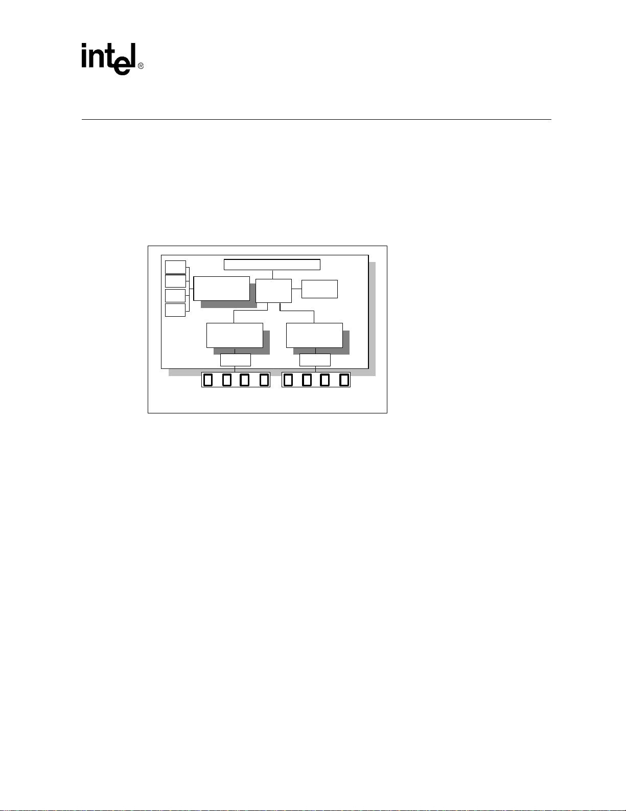
Fast Ethernet 10/100 Quad Transceivers — LXT974/LXT975
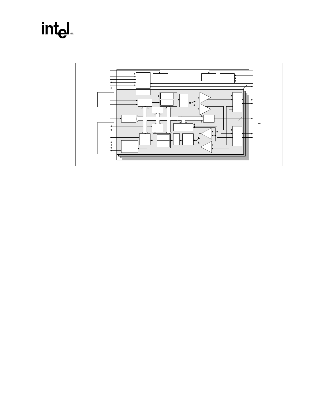
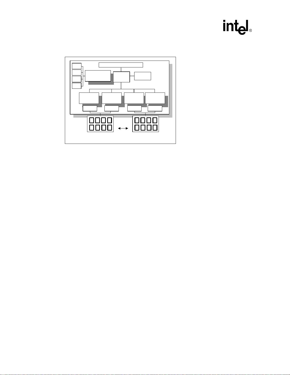
Figure 1. LXT974/975 Block Diagram
MII
MII
VCCMII
MII_MD<1:0>
CFG<2:0>
ADDR<4:2>
MDIO
MDC
MDINT
TX_ENn
TX_ERn
TXDn<3:0>
TRSTEn
TX_CLKn
RX_CLKn
RXDn<3:0>
CRSn
COLn
RX_DVn
RX_ERn
Tristate Control
Carrier Sense
Collision Detect
Data Valid
Error Detect
Management /
Mode Select
Logic
Register Set
Parallel/Serial
Converter
Serial to
Parallel
Converter
Global Functions
MII Power
Supply
3.3V or 5V
Manchester
10
Auto
Negotiation
Clock
Generator
Manchester
10
Decoder &
100
Descrambler
Encoder
Scrambler
& Encoder
Decoder
Pulse
100
Shaper
Media Select &
Line Energy Monitor
Slicer
Per-Port Functions
Baseline
Wander
Correction
Internal Clocks
TP
Driver
ECL
Driver
PORT 0
PORT 1
PORT 2
+
-
+
-
FDX Status
& LED
Drivers
TP
Rcvr
ECL
Rcvr
PORT 3
CLK25M
Pwr Supply /
PwrDown
TP Out
/
Fiber In
+
-
+
Fiber Out
/
TP In
VCC
GND
PWRDN
RESET
SerLED
3
LEDENA
LEDCLK
LEDDAT
TPOP/FIBINn
TPON/FIBIPn
LEDn<2:0>
3
SD/TXn
TPIP/FIBOPn
TPIN/FIBONn
-
Datasheet 9
Page 10
LXT974/LXT975 — Fast Ethernet 10/100 Quad Transceivers
1.0 Pin Assignments and Signal Descriptions
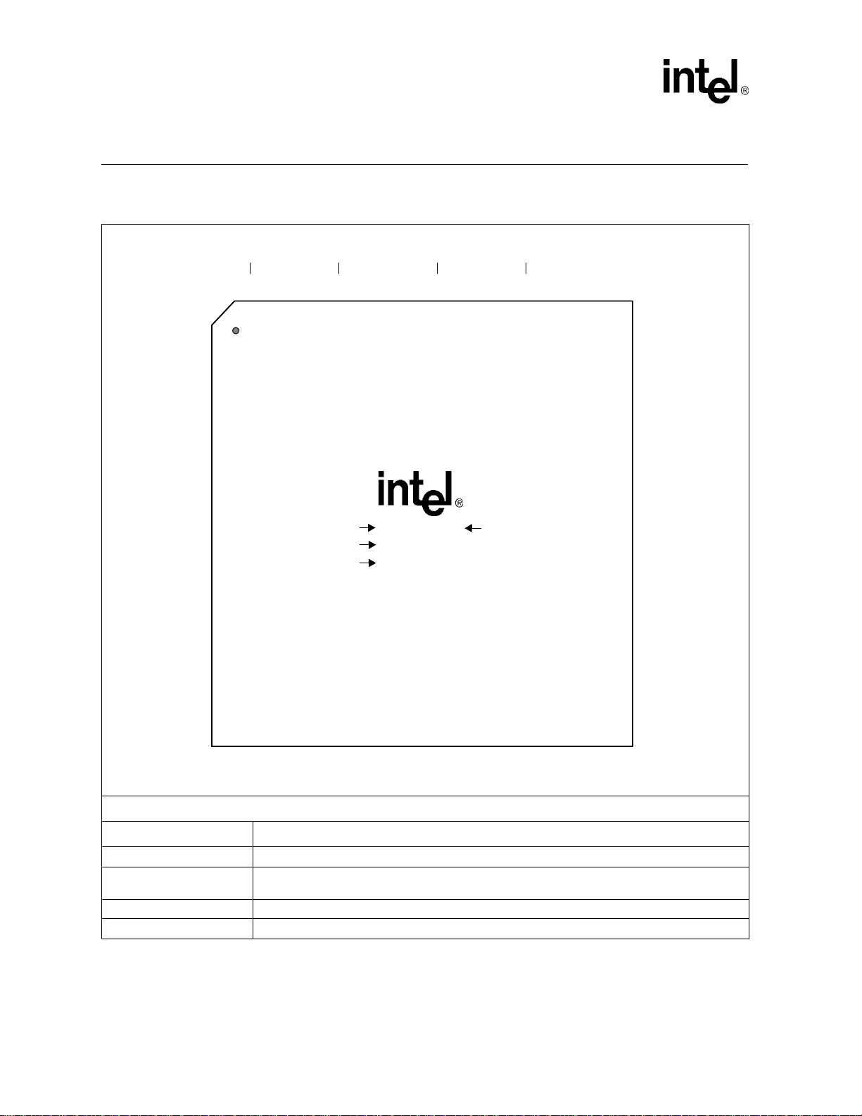
Figure 2. LXT974 Pin Assignments
160....... GND
159....... TEST
158....... SD0/TP0
157....... TPON/FIBIP0
156....... VCCT
155....... GNDT
154....... TPOP/FIBIN0
153....... VCCR
152....... TPIN/FIBON0
151....... TPIP/FIBOP0
150....... GNDR
149....... SD1/TP1
148....... TPON/FIBIP1
147....... VCCT
146....... GNDT
145....... TPOP/FIBIN1
144....... VCCR
143....... TPIN/FIBON1
142....... TPIP/FIBOP1
141....... GNDR
140....... RBIAS
139....... SD2/TP2
138....... TPON/FIBIP2
137....... VCCT
136....... GNDT
135....... TPOP/FIBIN2
134....... VCCR
133....... TPIN/FIBON2
132....... TPIP/FIBOP2
131....... GNDR
130....... SD3/TP3
129....... TPON/FIBIP3
128....... VCCT
127....... GNDT
126....... TPOP/FIBIN3
125....... VCCR
124....... TPIN/FIBON3
123....... TPIP/FIBOP3
122....... GNDR
121....... GNDR
LED3_0 .....1
LED3_1 .....2
LED3_2 .....3
LED2_0 .....4
LED2_1 .....5
LED2_2 .....6
GND .....7
LED1_0 .....8
LED1_1 .....9
LED1_2 .....10
LED0_0 .....11
LED0_1 .....12
LED0_2 .....13
GND .....14
LEDCLK .....15
LEDDAT .....16
LEDENA .....17
ADD2 .....18
ADD3 .....19
ADD4 .....20
GNDA .....21
VCC .....22
RXD0_3 .....23
RXD0_2 .....24
RXD0_1 .....25
RXD0_0 .....26
RX_DV0 .....27
RX_CLK0 .....28
RX_ER0 .....29
TX_ER0 .....30
TX_CLK0 ..... 31
TX_EN0 .....32
TXD0_0 .....33
TXD0_1 .....34
TXD0_2 .....35
TXD0_3 .....36
COL0 .....37
CRS0 ..... 38
GND .....39
VCCMII .....40
Part #
Part #
LOT #
LOT #
FPO #
FPO #
LXT974 XX
XXXXXX
XXXXXXXX
Rev #
120 .......N/C
119 .......N/C
118 .......CLK25M
117 .......FDE_FX
116 .......CFG_0
115 .......CFG_1
114 .......CFG_2
113 .......BYPSCR
112 .......TEST
111 .......AUTOENA
110 .......FDE
109 .......RESET
108 .......GNDH
107 .......VCCH
106 .......TRSTE0
105 .......TRSTE1
104 .......TRSTE2
103 .......TRSTE3
102 .......PWRDN
101 .......TEST
100 .......MDDIS
99 .........MDC
98 .........MDINT
97 .........MDIO
96 .........VCC
95 .........GND
94 .........CRS3
93 .........COL3
92 .........TXD3_3
91 .........TXD3_2
90 .........TXD3_1
89 .........TXD3_0
88 .........TX_EN3
87 .........TX_CLK3
86 .........TX_ER3
85 .........RX_ER3
84 .........RX_CLK3
83 .........RX_DV3
82 .........RXD3_0
81 .........RXD3_1
N/C .................41
RXD1_3 .......... 42
RXD1_2 .......... 43
RXD1_1 .......... 44
RXD1_0 .......... 45
RX_DV1.......... 46
RX_CLK1........ 47
RX_ER1.......... 48
TX_ER1 .......... 49
TX_CLK1........ 50
TX_EN1 .......... 51
TXD1_0 ..........52
TXD1_1 ..........53
TXD1_2 ..........54
TXD1_3 ..........55
GND................ 56
COL1 ..............57
CRS1 .............. 58
GND................ 59
VCC................ 60
RXD2_3 .......... 61
RXD2_2 .......... 62
RXD2_1 .......... 63
RXD2_0 .......... 64
RX_DV2.......... 65
RX_CLK2........ 66
RX_ER2.......... 67
TX_ER2 .......... 68
TX_CLK2........ 69
TX_EN2 .......... 70
TXD2_0 ..........71
TXD2_1 ..........72
TXD2_2 ..........73
TXD2_3 ..........74
COL2 ..............75
CRS2 .............. 76
GND................ 77
VCCMII ........... 78
RXD3_3 .......... 79
RXD3_2 .......... 80
Package Topside Markings
Marking Definition
Part # LXT974 is the unique identifier for this product family.
Rev #
Identifies the particular silicon “stepping” (Refer to Specification Update for additional stepping
information.)
Lot # Identifies the batch.
FPO # Identifies the Finish Process Order.
10 Datasheet
Page 11
Fast Ethernet 10/100 Quad Transceivers — LXT974/LXT975
Table 1. LXT974 Signal Detect/TP Select Signal Descriptions
2
Pin#
158
149
139
130
1. Type Column Coding: I = Input, O = Output.
2. When not using fiber mode, SD/TPn pins should be tied to GNDT.
Symbol Type
SD0/TP0
SD1/TP1
SD2/TP2
SD3/TP3
1
Signal Detect - Ports 0 - 3. When SD/TPn pins are tied High or to a 5V PECL input, bit
19.2 = 1 and the operating mode of each respective port is forced to FX mode. In this
mode, full-duplex is set via pin 117 (FDE_FX). When not using FX mode, SD/TPn pins
should be tied to GNDT.
TP Select - Ports 0 - 3. When SD/TPn pins are tied Low, bit 19.2 = 0. The operating mode
of each port can be set to 10BASE-T, 100BASE-TX, or 100BASE-FX via the hardware
I
control interface pins as shown in Table 8 on page 16.
Note: Hardware control interface pins (CFG_0, CFG_1, CFG_2, FDE, BYPSCR, and
AUTOENA) are global and set all ports simultaneously.
In TP mode, network pins operate as described in Tab le 2 .
In FX mode, network pins are re-mapped and operate as described in Table 3.
Signal Description
Table 2. LXT974 Twisted-Pair Interface Signal Descriptions
Pin# Symbol Type
1
Signal Description
154, 157
145, 148
135, 138
126, 129
151, 152
142, 143
132, 133
123, 124
1. Type Column Coding: I = Input, O = Output.
TPOP0, TPON0
TPOP1, TPON1
TPOP2, TPON2
TPOP3, TPON3
TPIP0, TPIN0
TPIP1, TPIN1
TPIP2, TPIN2
TPIP3, TPIN3
Twisted-Pair Outputs, Positive & Negative - Ports 0-3.
O
During 100BASE-TX or 10BASE-T operation, TPO pins drive 802.3 compliant
pulses onto the line.
Twisted-Pair Inputs, Positive & Negative - Ports 0-3.
I
During 100BASE-TX or 10BASE-T operation, TPI pins receive differential
100BASE-TX or 10BASE-T signals from the line.
Table 3. LXT974 Fiber Interface Signal Descriptions
Pin# Symbol Type
154, 157
145, 148
135, 138
126, 129
151, 152
142, 143
132, 133
123, 124
1. Type Column Coding: I = Input, O = Output.
FIBIN0, FIBIP0
FIBIN1, FIBIP1
FIBIN2, FIBIP2
FIBIN3, FIBIP3
FIBOP0, FIBON0
FIBOP1, FIBON1
FIBOP2, FIBON2
FIBOP3, FIBON3
1
Fiber Inputs, Positive & Negative - Ports 0-3.
I
During 100BASE-FX operation, FIBI pins receive differential PECL inputs
from fiber transceivers.
Fiber Outputs, Positive & Negative - Ports 0-3.
O
During 100BASE-FX operation, FIBO pins produce differential PECL
outputs for fiber transceivers.
Signal Description
Datasheet 11
Page 12
LXT974/LXT975 — Fast Ethernet 10/100 Quad Transceivers
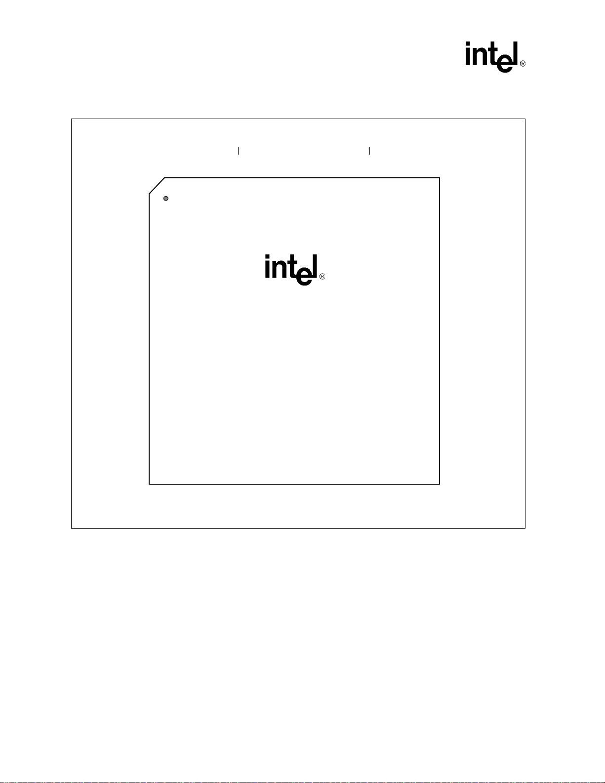
Figure 3. LXT975 Pin Assignments
160....... GND
159....... TEST
158....... TPIP0
157....... TPIN0
156....... GNDR
155....... TPOP0
154....... VCCT
153....... GNDT
152....... TPON0
151....... VCCR
150....... GNDR
149....... SD1/TP1
148....... TPON/FIBIP1
147....... VCCT
146....... GNDT
145....... TPOP/FIBIN1
144....... VCCR
143....... TPIN/FIBON1
142....... TPIP/FIBOP1
141....... GNDR
140....... RBIAS
139....... TPIP2
138....... TPIN2
137....... GNDR
LED3_0 .....1
LED3_1 .....2
LED3_2 .....3
LED2_0 .....4
LED2_1 .....5
LED2_2 .....6
GND .....7
LED1_0 .....8
LED1_1 .....9
LED1_2 .....10
LED0_0 .....11
LED0_1 .....12
LED0_2 .....13
GND .....14
LEDCLK .....15
LEDDAT .....16
LEDENA .....17
ADD2 .....18
ADD3 .....19
ADD4 .....20
GNDA .....21
VCC .....22
RXD0_3 .....23
RXD0_2 .....24
RXD0_1 .....25
RXD0_0 .....26
RX_DV0 .....27
RX_CLK0 .....28
RX_ER0 .....29
TX_ER0 .....30
TX_CLK0 ..... 31
TX_EN0 .....32
TXD0_0 .....33
TXD0_1 .....34
TXD0_2 .....35
TXD0_3 .....36
COL0 .....37
CRS0 .....38
GND .....39
VCCMII .....40
(Date Code)
(Part#)
(Lot#)
XXXX XXXX
LXT974AHC or
LXT974BHC
XXXXXX
136....... TPOP2
135....... VCCT
134....... GNDT
133....... TPON2
132....... VCCR
131....... GNDR
130....... SD3/TP3
129....... TPON/FIBIP3
128....... VCCT
127....... GNDT
126....... TPOP/FIBIN3
125....... VCCR
124....... TPIN/FIBON3
123....... TPIP/FIBOP3
122....... GNDR
121....... GNDR
120 .......N/C
119 .......N/C
118 .......CLK25M
117 .......FDE_FX
116 .......CFG_0
115 .......CFG_1
114 .......CFG_2
113 .......BYPSCR
112 .......TEST
111 .......AUTOENA
110 .......FDE
109 .......RESET
108 .......GNDH
107 .......VCCH
106 .......TRSTE0
105 .......TRSTE1
104 .......TRSTE2
103 .......TRSTE3
102 .......PWRDN
101 .......TEST
100 .......MDDIS
99 .........MDC
98 .........MDINT
97 .........MDIO
96 .........VCC
95 .........GND
94 .........CRS3
93 .........COL3
92 .........TXD3_3
91 .........TXD3_2
90 .........TXD3_1
89 .........TXD3_0
88 .........TX_EN3
87 .........TX_CLK3
86 .........TX_ER3
85 .........RX_ER3
84 .........RX_CLK3
83 .........RX_DV3
82 .........RXD3_0
81 .........RXD3_1
N/C .................41
RXD1_3 .......... 42
RXD1_2 .......... 43
RXD1_1 .......... 44
RXD1_0 .......... 45
RX_DV1.......... 46
RX_CLK1........ 47
RX_ER1.......... 48
TX_ER1 .......... 49
TX_CLK1 ........ 50
TX_EN1 .......... 51
TXD1_0 ..........52
TXD1_1 ..........53
TXD1_2 ..........54
TXD1_3 ..........55
GND................ 56
COL1 ..............57
CRS1 ..............58
GND................ 59
VCC ................ 60
RXD2_3 .......... 61
RXD2_2 .......... 62
RXD2_1 .......... 63
RXD2_0 .......... 64
RX_DV2.......... 65
RX_CLK2........ 66
RX_ER2.......... 67
TX_ER2 .......... 68
TX_CLK2 ........ 69
TX_EN2 .......... 70
TXD2_0 ..........71
TXD2_1 ..........72
TXD2_2 ..........73
TXD2_3 ..........74
COL2 ..............75
CRS2 ..............76
GND................ 77
VCCMII ........... 78
RXD3_3 .......... 79
RXD3_2 .......... 80
12 Datasheet
Page 13
Fast Ethernet 10/100 Quad Transceivers — LXT974/LXT975
Table 4. LXT975 Signal Detect/TP Select Signal Descriptions
2
Pin#
149
130
1. Type Column Coding: I = Input, O = Output.
2. When not using fiber mode, SD/TPn pins should be tied to GNDT.
Symbol Type
SD1/TP1
SD3/TP3
1
Signal Detect - Ports 1 & 3. When SD/TPn pins are tied High or to a 5V PECL input, bit
19.2 = 1 and the operating mode of each respective port is forced to FX mode. In this
mode, full-duplex is set via pin 117 (FDE_FX). When not using fiber mode, SD/TPn pins
should be tied to GNDT.
TP Select - Ports 1 & 3. When SD/TPn pins are tied Low, bit 19.2 = 0. The operating mode
of each port can be set to 10BASE-T, 100BASE-TX, or 100BASE-FX via the hardware
I
control interface pins as shown in Table 8 on page 16.
Note: Hardware control interface pins (CFG_0, CFG_1, CFG_2, FDE, BYPSCR, and
AUTOENA) are global and set all ports simultaneously.
In TP mode, network pins operate as described in Tab le 5 .
In FX mode, network pins are re-mapped and operate as described in Table 6.
Signal Description
Table 5. LXT975 Twisted-Pair Interface Signal Descriptions
Pin# Symbol Type
1
Signal Description
155, 152
145, 148
136, 133
126, 129
158, 157
142, 143
139, 138
123, 124
1. Type Column Coding: I = Input, O = Output.
TPOP0, TPON0
TPOP1, TPON1
TPOP2, TPON2
TPOP3, TPON3
TPIP0, TPIN0
TPIP1, TPIN1
TPIP2, TPIN2
TPIP3, TPIN3
Twisted-Pair Outputs, Positive & Negative - Ports 0-3.
O
During 100BASE-TX or 10BASE-T operation, TPO pins drive 802.3 compliant
pulses onto the line.
Twisted-Pair Inputs, Positive & Negative - Ports 0-3.
I
During 100BASE-TX or 10BASE-T operation, TPI pins receive differential
100BASE-TX or 10BASE-T signals from the line.
Table 6. LXT975 Fiber Interface Signal Descriptions
Pin# Symbol Type
145, 148
126, 129
142, 143
123, 124
1. Type Column Coding: I = Input, O = Output.
FIBIN1, FIBIP1
FIBIN3, FIBIP3
FIBOP1, FIBON1
FIBOP3, FIBON3
1
Fiber Network Interface - Ports 1 and 3
I
During 100BASE-FX operation, FIBI pins receive differential PECL inputs
from fiber transceivers.
Fiber Network Interface - Ports 1 and 3
O
During 100BASE-FX operation, FIBO pins produce differential PECL
outputs for fiber transceivers.
Signal Description
Datasheet 13
Page 14

LXT974/LXT975 — Fast Ethernet 10/100 Quad Transceivers
Table 7. LXT974 and LXT975 MII Signal Descriptions
3
Pin#
33
34
35
36
52
53
54
55
71
72
73
74
89
90
91
92
32
51
70
88
31
50
69
87
30
49
68
86
26
25
24
23
45
44
43
42
64
63
62
61
82
81
80
79
1. Type Column Coding: I = Input, O = Output, OD = Open Drain
2. The LXT974/975 supports the 802.3 MDIO register set. Specific bits in the registers are referenced using an “X.Y” notation,
where X is the register number (0-6 or 16-20) and Y is the bit number (0-15).
3. Unused pins should be tied Low.
Symbol Type
TXD0_0
TXD0_1
TXD0_2
TXD0_3
TXD1_0
TXD1_1
TXD1_2
TXD1_3
TXD2_0
TXD2_1
TXD2_2
TXD2_3
TXD3_0
TXD3_1
TXD3_2
TXD3_3
TX_EN0
TX_EN1
TX_EN2
TX_EN3
TX_CLK0
TX_CLK1
TX_CLK2
TX_CLK3
TX_ER0
TX_ER1
TX_ER2
TX_ER3
RXD0_0
RXD0_1
RXD0_2
RXD0_3
RXD1_0
RXD1_1
RXD1_2
RXD1_3
RXD2_0
RXD2_1
RXD2_2
RXD2_3
RXD3_0
RXD3_1
RXD3_2
RXD3_3
1
MII Data Interface Pins
I Transmit Data - Port 0. Inputs containing NRZ data to be transmitted from port 0.
I Transmit Data - Port 1. Inputs containing NRZ data to be transmitted from port 1.
I Transmit Data - Port 2. Inputs containing NRZ data to be transmitted from port 2.
I Transmit Data - Port 3. Inputs containing NRZ data to be transmitted from port 3.
Transmit Enable - Ports 0 - 3. Active High input enables respective port transmitter. This
I
signal must be synchronous to the TX_CLK.
Transmit Clock - Ports 0 - 3. 25 MHz for 100 Mbps operation, 2.5 MHz for 10 Mbps
operation. The transmit data and control signals must always be synchronized to TX_CLK
by the MAC. The LXT974/975 normally samples these signals on the rising edge of
O
TX_CLK. However, Advanced TX_CLK Mode is available by setting MII register bit 19.5=1.
In this mode, the LXT974/975 samples the transmit data and control signals on the falling
edge of TX_CLK.
Transmit Coding Error - Ports 0 - 3. This signal must be driven synchronously to TX_CLK.
I
When High, forces the respective port to transmit Halt (H) code group.
Receive Data - Port 0. Receive data signals (4-bit parallel nibbles) are driven synchronously
O
to RX_CLK0.
Receive Data - Port 1. Receive data signals (4-bit parallel nibbles) are driven synchronously
O
to RX_CLK1.
Receive Data - Port 2. Receive data signals (4-bit parallel nibbles) are driven synchronously
O
to RX_CLK2.
Receive Data - Port 3. Receive data signals (4-bit parallel nibbles) are driven synchronously
O
to RX_CLK3.
Signal Description
2
14 Datasheet
Page 15

Fast Ethernet 10/100 Quad Transceivers — LXT974/LXT975
Table 7. LXT974 and LXT975 MII Signal Descriptions (Continued)
Pin#
27
46
65
83
29
48
67
85
28
47
66
84
37
57
75
93
38
58
76
94
3
Symbol Type
RX_DV0
RX_DV1
RX_DV2
RX_DV3
RX_ER0
RX_ER1
RX_ER2
RX_ER3
RX_CLK0
RX_CLK1
RX_CLK2
RX_CLK3
COL0
COL1
COL2
COL3
CRS0
CRS1
CRS2
CRS3
1
Receive Data Valid - Ports 0 - 3. These signals are synchronous to the respective
O
RX_CLKn. Active High indication that received code group maps to valid data.
Receive Error - Ports 0 - 3. These signals are synchronous to the respective RX_CLKn.
O
Active High indicates that received code group is invalid, or that PLL is not locked.
O Receive Clock - Ports 0 - 3. 25 MHz for 100 Mbps and 2.5 MHz for 10 Mbps.
Collision Detected - Ports 0 - 3. Active High outputs asserted upon detection of a collision.
O
Remain High for the duration of the collision. These signals are generated asynchronously.
Inactive during full-duplex operation.
Carrier Sense - Ports 0 - 3. Active High signals. During half-duplex operation
(bit 0.8 = 0), CRSn is asserted when either transmit or receive medium is non-idle. During
O
full-duplex operation (bit 0.8 = 1), CRSn is asserted only when the receive medium is nonidle.
Signal Description
2
MII Control Interface Pins
97 MDIO I/O
98 MDINT OD
99 MDC I
100 MDDIS I
TRSTE0
106
TRSTE1
105
TRSTE2
104
TRSTE3
103
1. Type Column Coding: I = Input, O = Output, OD = Open Drain
2. The LXT974/975 supports the 802.3 MDIO register set. Specific bits in the registers are referenced using an “X.Y” notation,
where X is the register number (0-6 or 16-20) and Y is the bit number (0-15).
3. Unused pins should be tied Low.
Management Data Input/Output. Bidirectional serial data channel for PHY/STA
communication.
Management Data Interrupt. An active Low output on this pin indicates status change.
Interrupt is cleared by sequentially reading Register 1, then Register 18.
Management Data Clock. Clock for the MDIO serial data channel.
Maximum frequency is 2.5 MHz.
Management Disable.
When MDDIS is High, the MDIO is restricted to Read Only and the Hardware Control
Interface pins provide continual control of their respective bits.
When MDDIS is Low at power up or Reset, the Hardware Control Interface pins control only
the initial or “default” values of their respective register bits. After the power-up/reset cycle is
complete, bit control reverts to the MDIO serial channel.
Tristate - Ports 0 - 3. This bit controls bit 0.10 (Isolate bit). When TRSTEn is High, the
respective port isolates itself from the MII Data Interface.
I
When MDDIS is High, TRSTE provides continuous control over bit 0.10.
When MDDIS is Low, TRSTE sets the initial (default) value of bit 0.10 at Reset and then bit
control reverts back to the MDIO interface.
Datasheet 15
Page 16

LXT974/LXT975 — Fast Ethernet 10/100 Quad Transceivers
Table 8. LXT974 and LXT975 Hardware Control Interface Signal Descriptions
Pin# Symbol Type
CFG_0
116
(Global)
CFG_1
115
(Global)
CFG_2
114
(Global)
FDE
110
(Global)
FDE_FX
117
BYPSCR
113
(Global)
AUTOENA
111
(Global)
1. Type Column Coding: I = Input, O = Output, OD = Open Drain.
2. The LXT974/975 supports the 802.3 MDIO register set. Specific bits in the registers are referenced using an “X.Y” notation,
where X is the register number (0-6 or 16-20) and Y is the bit number (0-15).
1
Configuration Control 0.
When A/N is enabled, Low to High transition on CFG_0 causes auto-negotiate to restart on
all ports and 0.9 = 1.
I
When A/N is disabled, this input selects operating speed and directly affects bit 0.13.
When CFG_0 is High, 100 Mbps is selected and bit 0.13 = 1.
When CFG_0 is Low, 10 Mbps is selected and bit 0.13 = 0.
Configuration Control 1.
When A/N is enabled, CFG_1 determines operating speed advertisement capabilities in
combination with CFG_2 and FDE on all ports. See Table 16 on page 26 for details.
I
When A/N is disabled, CFG_1 enables 10 Mbps link test and directly affects bit 19.8.
When CFG_1 is High, 10 Mbps link test is disabled and bit 19.8 = 1.
When CFG_1 is Low, 10 Mbps link test is enabled and bit 19.8 = 0.
Configuration Control 2.
When A/N is enabled, CFG_2 determines operating speed advertisement capabilities in
combination with CFG_1 on all ports. See Table 16 on page 26 for details.
When A/N is disabled, this input selects either TP or FX interface. When FX interface is
selected, the LXT974/975 automatically disables the scrambler. For correct FX operation,
100 Mbps operation must also be selected.
I
Note: It is recommended to set the network interface for each port independently, via the SD/
TPn pins. See Table 1 and Table 4 for Signal Detect / TP Select signal descriptions and
operation.
When CFG_2 is Low, TP is enabled and bit 19.2 = 0.
When CFG_2 is High, FX is enabled and bit 19.2 = 1.
Full-Duplex Enable - All Ports.
I
When High, enables full-duplex operation on all ports.
Full-Duplex Enable - FX Ports only.
I
When High, enables full-duplex operation on all ports set for FX mode operation. This pin is
ignored on ports set for TP mode.
Bypass Scrambler.
In TP mode, enables or bypasses Scrambler operation and directly affects MDIO
register bit 19.3.
When High, Scrambler is bypassed and bit 19.3 = 1.
I
When Low, Scrambler is enabled and bit 19.3 = 0.
In FX mode, the LXT974/975_ automatically bypasses the Scrambler. This pin has no
effect selecting Scrambler bypass.
I Auto-Negotiation Enable. When High, enables auto-negotiation on all ports.
Signal Description
2
16 Datasheet
Page 17
Fast Ethernet 10/100 Quad Transceivers — LXT974/LXT975
Table 9. LXT974 and LXT975 Miscellaneous Signal Descriptions
Pin# Symbol Type
1
Signal Description
2
ADD1 ADD0 Port
Address <4:2>. Set upper three bits of PHY
20
19
18
101, 112, 159 TEST I Test. Must be tied Low.
140 RBIAS I
118 CLK25M I
109 RESET I
102 PWRDN I
41, 119, 120 N/C - No Connection. Leave open.
1. Type Column Coding: I = Input, O = Output, A = Analog.
2. The LXT974/975 supports the 802.3 MDIO register set. Specific bits in the registers are referenced using an “X.Y” notation,
where X is the register number (0-6 or 16-20) and Y is the bit number (0-15).
ADD4
ADD3
ADD2
I
address. ADD<1:0> are set internally to match
I
port number as shown at right.
I
Bias. This pin provides bias current for the internal circuitry. Must be tied to
ground through a 22 k
Clock Input. A 25 MHz clock input is required at this pin. Refer to Functional
Description for detailed clock requirements.
Reset. This active Low input is OR’ed with the control register Reset bit (0.15).
The LXT974/975 reset cycle is extended 205
asserted.
Power Down. When High, forces LXT974/975 into power down mode. This pin is
OR’ed with the Power Down bit (0.11). Refer to Table 44 on page 64 for more
information.
Ω resistor.
µs (nominal) after Reset is de-
00 0
01 1
10 2
11 3
Table 10. LXT974 and LXT975 LED Indicator Signal Descriptions
2
Pin#
11
12
13
10
17 LEDENA O LED Enable. Active High output signals external device that LEDDAT is active.
15 LEDCLK O LED Clock. 25 MHz clock for LED serial data output.
16 LEDDAT O LED Data. Serial data output for 24 LEDs (6 x 4 ports) data.
1. Type Column Coding: I = Input, O = Output, OD = Open Drain.
2. Unused pins should be tied Low.
3. The LXT974/975 supports the 802.3 MDIO register set. Specific bits in the registers are referenced using an “X.Y” notation,
Symbol Type
LED0_0
LED1_0
8
LED2_0
4
LED3_0
1
LED0_1
LED1_1
9
LED2_1
5
LED3_1
2
LED0_2
LED1_2
LED2_2
6
LED3_2
3
where X is the register number (0-6 or 16-20) and Y is the bit number (0-15).
OD
OD
OD
1
LED0 - Ports 0 - 3. In default mode, active Low output indicates transmitter active. However,
LED0 is programmable and may also be set to indicate receiver active, link status or duplex
status. Refer to LED Configuration Register, Table 51 on page 68, for details on
programming options.
LED1 - Ports 0 - 3. In default mode, active Low output indicates receiver active. However,
LED1 is programmable and may also be set to indicate link status, duplex status, or operating
speed. Refer to LED Configuration Register, Table 51 on page 68, for details on
programming options.
LED2 - Ports 0 - 3. In default mode, active Low output indicates link up. However, LED2 is
programmable and may also be set to indicate duplex status, operating speed or collision.
Refer to LED Configuration Register, Table 51 on page 68, for details on
programming options.
Signal Description
3
Datasheet 17
Page 18
LXT974/LXT975 — Fast Ethernet 10/100 Quad Transceivers
Table 11. LXT974 Power Supply Signal Descriptions
Pin# Symbol Type Signal Description
22, 60, 96 VCC - Power Supply. +5V supply for all digital circuits.
40, 78 VCCMII -
7, 14, 39, 56, 59, 77, 95, 160 GND - Digital Ground. Ground return for digital supply.
21 GNDA - Analog Ground. Ground return for analog supply.
108 GNDH - Ground. Ground return for core analog circuitry.
107 VCCH - Supply. +5V supply for core analog circuitry.
128, 137, 147, 156 VCCT - Transmit Power Supply. +5V supply for transmit circuits.
127, 136, 146, 155 GNDT - Transmit Ground. Ground return for transmit supply.
125, 134, 144, 153, VCCR - Receive Power Supply. +5V supply for all receive circuits.
121, 122, 131, 141, 150 GNDR - Receive Ground. Ground return for receive supply.
MII Supply. +3.3V or +5V supply for MII. A decoupling capacitor
to digital ground should be supplied for these pins.
Table 12. LXT975 Power Supply Signal Descriptions
Pin# Symbol Type Signal Description
22, 60, 96 VCC - Power Supply. +5V supply for all digital circuits.
40, 78 VCCMII -
7, 14, 39, 56, 59, 77, 95, 160 GND - Digital Ground. Ground return for digital supply.
21 GNDA - Analog Ground. Ground return for analog supply.
108 GNDH - Ground. Ground return for core analog circuitry.
107 VCCH - Supply. +5V supply for core analog circuitry.
128, 135, 147, 154 VCCT - Transmit Power Supply. +5V supply for transmit circuits.
127, 134, 146, 153 GNDT - Transmit Ground. Ground return for transmit supply.
125, 132, 144, 151, VCCR - Receive Power Supply. +5V supply for all receive circuits.
121, 122, 131, 137, 141, 150, 156 GNDR - Receive Ground. Ground return for receive supply.
MII Supply. +3.3V or +5V supply for MII. A decoupling capacitor
to digital ground should be supplied for these pins.
18 Datasheet
Page 19
Fast Ethernet 10/100 Quad Transceivers — LXT974/LXT975
2.0 Functional Description
2.1 Introduction
The LXT974 and LXT975 are four-port Fast Ethernet 10/100 Transceivers that support 10 Mbps
and 100 Mbps networks. They comply with all applicable requirements of IEEE 802.3. Each port
can directly drive either a 100BASE-TX line (>130 meters) or a 10BASE-T line (>185 meters).
Figure 4 shows the LXT974 in a typical switch application.
Figure 4. LXT974 Switch Application
Fiber
Module
Fiber
Module
Fiber
Module
Fiber
Module
LXT974
10/100
Quad Transceiver
LXT974
10/100
Quad Transceiver
Transformer
Backplane
Switch
MAC ASIC
QUAD
Single RJ-45
Selectable 10 or 100 Mbps
Memory
LXT974
10/100
Quad Transceiver
QUAD
Transformer
On power-up, the LXT974/975 uses auto-negotiation/parallel detection on each port to
automatically determine line operating conditions. If the PHY device on the other side of the link
supports auto-negotiation, the LXT974/975 auto-negotiates with it using Fast Link Pulse (FLP)
Bursts. If the PHY partner does not support auto-negotiation, the LXT974/975 automatically
detects the presence of either link pulses (10 Mbps PHY) or Idle symbols (100 Mbps PHY) and set
its operating conditions accordingly.
The LXT974/975 interfaces to four 10/100 Media Access Controllers (MAC)s through the MII
interfaces. It performs all functions of the Physical Coding Sublayer (PCS) and Physical Media
Attachment (PMA) sublayer as defined in the IEEE 802.3 100BASE-X specification. This device
also performs all functions of the Physical Media Dependent (PMD) sublayer for 100BASE-TX
connections. The MII speeds are automatically set once port operating conditions have been
determined.
The LXT974/975 provides half-duplex and full-duplex operation at 100 Mbps and 10 Mbps. It also
offers standard Loopback Mode for switch applications. The LXT974/975 supports the 802.3
MDIO register set. Specific bits in the registers are referenced using an “X.Y” notation, where X is
the register number (0-6 or 16-20) and Y is the bit number (0-15).
The LXT975 is pin compatible with the LXT974 except for the network ports. Each port on the
LXT974 provides a combination twisted-pair or PECL interface for a 10/100BASE-TX or
100BASE-FX connection.
The LXT975 is optimized for stacked RJ-45 modular applications as shown in Figure 5. Ports 1
and 3 support the PECL interface for fiber connections and all four ports support the twisted-pair
interface for 10/100BASE-TX connections.
Datasheet 19
Page 20
LXT974/LXT975 — Fast Ethernet 10/100 Quad Transceivers
Figure 5. LXT975 Switch Application
Fiber
Module
Fiber
Module
Fiber
Module
Fiber
Module
LXT974
10/100
Quad Transceiver
LXT975
10/100 Quad
Transceiver
QUAD
Transformer
Backplane
MAC ASIC
LXT975
10/100 Quad
Transceiver
QUAD
Transformer
Stacked RJ-45
10 or 100 Mbps
Switch
Memory
LXT975
10/100 Quad
Transceiver
QUAD
Transformer
LXT975
10/100 Quad
Transceiver
QUAD
Transformer
2.2 Network Media / Protocol Support
The LXT974/975 supports both 10BASE-T and 100BASE-TX Ethernet over twisted-pair, or 100
Mbps Ethernet over fiber media (100BASE-FX). A Media Independent Interface (MII) is used for
communication with the Media Access Controller (MAC).
2.2.1 10/100 Mbps Network Interface
Each of the four network interface ports consists of four external pins (two differential signal
pairs). The pins are shared between twisted-pair (TP) and fiber. Signal assignments (input or
output, positive or negative) vary depending on whether the port is configured for TP or fiber
media. Refer to Table 1 through Table 6 for specific pin assignments.
The LXT974/975 output drivers generate either 100BASE-TX, 10BASE-T, or 100BASE-FX
output. When not transmitting data, the LXT974/975 generates 802.3-compliant link pulses or idle
code. Input signals are decoded either as a 100BASE-TX, 100BASE-FX, or 10BASE-T input,
depending on the mode selected. Auto-negotiation/parallel detection or manual control is used to
determine the speed of this interface.
2.2.1.1 Twisted-Pair Interface
When operating at 100 Mbps, MLT3 symbols are continuously transmitted and received. When not
transmitting data, the LXT974/975 generates “IDLE” symbols.
During 10 Mbps operation, Manchester-encoded data is exchanged. When no data is being
exchanged, the line is left in an idle state.
In 100 Mbps mode, the LXT974/975 is capable of driving a 100BASE-TX connection over 100
Category 5, Unshielded Twisted Pair (UTP). A 10BASE-T connection can be supported using
Ω Category 3, UTP.
100
Ω,
20 Datasheet
Page 21

Only a transformer (1:1 on receive side, 2:1 on transmit side), load resistors, and bypass capacitors
are needed to complete this interface. Using Intel’s patented waveshaping technology, the
transmitter pre-distorts the outgoing signal to reduce the need for external filters for EMI
compliance.
Ω passive load is always present across the twisted-pair inputs. When enabled, the twisted-
A 4k
pair inputs are actively biased to approximately 2.8V.
2.2.1.2 Fiber Interface
The LXT974/975 provides a PECL interface that complies with the ANSI X3.166 specification.
This interface is suitable for driving a fiber-optic coupler.
The twisted-pair pin assignments are remapped to support the PECL interface. The LXT974
supports both the twisted-pair and fiber interface on all four ports. The LXT975, optimized for TP
operation with dual-high RJ-45 connectors, provides dual interfaces on ports 1 and 3.
During 100BASE-FX operation, the FIBI pins receive differential PECL signals and the FIBO pins
produce differential PECL output signals.
Fiber ports cannot be enabled via auto-negotiation; they must be enabled via the Hardware Control
Interface or MDIO registers.
Fast Ethernet 10/100 Quad Transceivers — LXT974/LXT975
2.2.2 MII Interface
The LXT974/975 supports four standard MIIs (one per port). This interface consists of a data
interface and a management interface. The MII Data Interface passes data between the LXT974/
975 and one or more Media Access Controllers (MACs). Separate signals are provided for
transmit and receive. This interface operates at either 10 Mbps or 100 Mbps. The speed is set
automatically, once the operating conditions of the network link have been determined.
Nine signals are used to pass received data to the MAC: RXD<3:0>, RX_CLK, RX_DV, RX_ER,
COL and CRS. Seven signals are used to transmit data from the MAC: TXD<3:0>, TX_CLK,
TX_EN, and TX_ER.
2.2.2.1 MII Data Interface
Figure 6 shows the data portion of the MII interface. Separate channels are provided for
transmitting data from the MAC to the LXT974/975 (TXD), and for receiving data (RXD) from the
line.
Each channel has its own clock, data bus, and control signals. The LXT974/975 supplies both
clock signals as well as separate outputs for carrier sense and collision. Data transmission across
the MII is implemented in 4-bit-wide nibbles.
Tristating the MII
The LXT974/975 asserts RX_DV, RXD, RX_CLK and RX_ER as soon as it receives a packet from
the network. When TRSTEn is High, the associated port output signals are tristated.
Datasheet 21
Page 22
LXT974/LXT975 — Fast Ethernet 10/100 Quad Transceivers
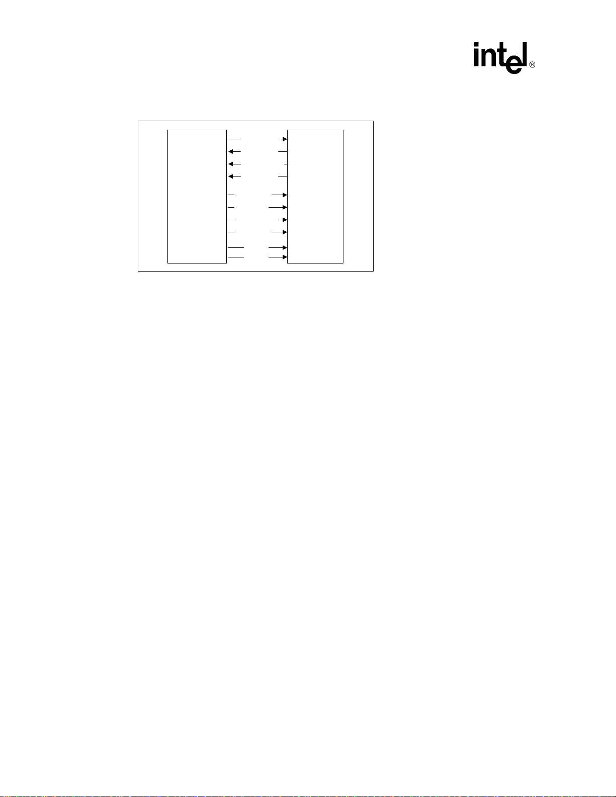
Figure 6. MII Data Interface
TX_CLKn
TX_ENn
TXD<3:0>n
LXT974/975
TX_ERn
RX_CLKn
RX_DVn
RXD<3:0>n
RX_ERn
CRSn
COLn
Media Access
Controller
MAC
Transmit Clock
The LXT974/975 is the master clock source for data transmission. The LXT974/975 automatically
sets the speed of TX_CLK to match port conditions. If the port is operating at 100 Mbps, TX_CLK
is set to 25 MHz. If the port is operating at 10 Mbps, TX_CLK is set to 2.5 MHz. The transmit data
and control signals must always be synchronized to TX_CLK by the MAC. The LXT974/975
normally samples these signals on the rising edge of TX_CLK.
However, Advanced TX_CLK Mode is available by setting MII register bit 19.5=1. In this mode,
the LXT974/975 samples the transmit data and control signals on the falling edge of TX_CLK.
When operating under MDIO Control, the user can advance the transmit clock relative to
TXD<3:0> and TX_ER. When Advance TX_CLK Mode is selected, the LXT974/975 clocks TXD
data in on the falling edge of TX_CLK, instead of the rising edge. This mode provides an increase
in timing margins of TXD, relative to TX_CLK. Advance TX_CLK Mode is enabled when bit 19.5
= 1.
Transmit Enable
The MAC must assert TX_EN the same time as the first nibble of preamble, and de-assert TX_EN
after the last bit of the packet.
Receive Data Valid
The LXT974/975 asserts RX_DV when it receives a valid packet. Timing changes depend on line
operating speed:
• For 100TX and 100FX links, RX_DV is asserted from the first nibble of preamble to the last
nibble of the data packet.
• For 10BT links, the entire preamble is truncated. RX_DV is asserted with the first nibble of
the Start of Frame Delimiter (SFD) “5D” and remains asserted until the end of the packet.
Error Signals
Whenever the LXT974/975 receives an errored symbol from the network, it asserts RX_ER and
drives “1110” on the RXD pins.
When the MAC asserts TX_ER, the LXT974/975 drives “H” symbols out on the line.
22 Datasheet
Page 23

Fast Ethernet 10/100 Quad Transceivers — LXT974/LXT975
Carrier Sense
Carrier sense (CRS) is an asynchronous output. It is always generated when a packet is received
from the line and in some modes when a packet is transmitted.
On transmit, CRS is asserted on a 10 Mbps or 100 Mbps half-duplex link. Carrier sense is not
generated on transmit when the link is operating in full-duplex mode.
Usage of CRS for Interframe Gap (IFG) timing is not recommended for the following reasons:
• De-assertion time for CRS is slightly longer than assertion time. This causes IFG intervals to
appear somewhat shorter to the MAC than it actually is on the wire.
• CRS de-assertion is not aligned with TX_EN de-assertion on transmit loopbacks in half-
duplex mode.
Operational Loopback
Operational loopback is provided for 10 Mbps half-duplex links when bit 19.11 = 0. Data
transmitted by the MAC is looped back on the receive side of the MII. Operational loopback is not
provided for 100 Mbps links, full-duplex links, or when 19.11 = 1.
Test Loopback
A test loopback function is provided for diagnostic testing of the LXT974/LXT975. During test
loopback, twisted-pair and fiber interfaces are disabled. Data transmitted by the MAC is internally
looped back by the LXT974/975 and returned to the MAC.
Test loopback is available for 100TX, 100FX, and 10T operation. Test loopback is enabled by
setting bit 0.14 = 1, bit 0.8 = 1 (full-duplex), and bit 0.12 = 0 (disable auto-negotiation). The
desired mode of operation for test loopback is set using bits 0.13 and 19.2 as shown in Table 13.
Loopback paths for the three modes of operation are shown in Figure 7.
Table 13. Test Loopback Operation
Mode of Operation
10T Test Loopback 0 0
100TX Test Loopback 0 1
100FX Test Loopback 1 1
1. Bit 0.14 = 1, bit 0.8 = 1, and 0.12 = 0 must also be set to enable Test Loopback.
Bit
19.2 0.13
Datasheet 23
Page 24

LXT974/LXT975 — Fast Ethernet 10/100 Quad Transceivers
Figure 7. Loopback Paths
100FX
Loopback
Analog
Block
100TX
Loopback
MII
10T
Loopback
Digital
Block
Collision
The LXT974/975 asserts its collision signal, asynchronously to any clock, whenever the line state
is half-duplex and the transmitter and receiver are active at the same time. Table 14 summarizes the
conditions for assertion of carrier sense, collision, and data loopback signals.
Table 14. Carrier Sense, Loopback, and Collision Conditions
Speed & Duplex Condition Carrier Sense Loopback Collision
Full-Duplex at 10 Mbps or 100 Mbps Receive Only None None
100 Mbps, Half-Duplex Transmit or Receive None Transmit and Receive
10 Mbps, Half-Duplex, 19.11 = 0 Transmit or Receive Yes Transmit and Receive
10 Mbps, Half-Duplex, 19.11 = 1 Transmit or Receive None Transmit and Receive
2.2.2.2 MII Management Interface
FX
Driver
TX
Driver
The LXT974/975 supports the IEEE 802.3 MII Management Interface also known as the
Management Data Input/Output (MDIO) Interface. This interface allows upper-layer devices to
monitor and control the state of the LXT974/975. The MDIO interface consists of a physical
connection, a specific protocol that runs across the connection, and an internal set of addressable
registers. Some registers are required and their functions are defined by the IEEE 802.3
specification. Additional registers are allowed for expanded functionality. The LXT974/975 is
configured with both sets of registers.
The physical interface consists of a data line (MDIO) and clock line (MDC). Operation of this
interface is controlled by the MDDIS input pin. When MDDIS is High, the MDIO operates as a
read-only interface. When MDDIS is Low, both read and write are enabled. The timing for the
MDIO Interface is shown in Table 40 on page 61. The protocol is shown in Figure 8 and Figure 9
(read and write). The protocol allows one controller to communicate with up to eight LXT974/975
chips. Bits A4:2 of the 5-bit PHY address are assigned as the LXT974/975 address. Bits A1:0 are
assigned as port addresses 0 through 3. The LXT974/975 supports 12 internal registers per port (48
total), each of which is 16 bits wide.
24 Datasheet
Page 25

Fast Ethernet 10/100 Quad Transceivers — LXT974/LXT975
Figure 8. Management Interface - Read Frame Structure
MDC
MDIO
(Read)
32 "1"s
Preamble SFD Op Code PHY Address
Idle
0110
A4 A3 A0 R4 R3 R0
Register Address
Write Read
Figure 9. Management Interface - Write Frame Structure
MDC
MDIO
(Write)
32 "1"s 0101
Preamble SFD Op Code PHY Address
Idle
A4 A3 A0 R4 R3 R0
Register Address
Write
MII Interrupts
The LXT974/975 provides interrupt signals in two ways. The MDIO interrupt reflects the interrupt
status of each port addressed by the read. Details are shown in Figure 10.
Setting bit 17.1 = 1 on all four ports, enables global interrupts using the MDINT pin. An active
Low on this pin indicates a status change on the LXT974/975. Interrupts may be caused by:
• Link status change
• Auto-negotiation complete
• Full-duplex status change
Z0
Turn
Around
1
Turn
Around
D15 D14
D15 D14 D1 D0
Data
D15 D14 D1 D0
0
Data Idle
D1
Idle
• Jabber detect
Figure 10. MDIO Interrupt Signaling
MDC
MDIO
Interrupt
Z
0
Turn
Around
MDIO FRAME
Read Data
Sourced by PHY
INT
Idle
2.2.3 Hardware Control Interface
The Hardware Control Interface is used to configure operating characteristics of the LXT974/975.
When MDDIS is Low, this interface provides initial values for the MDIO registers, and then
passes control to the MDIO Interface. When MDDIS is High, this interface provides continuous
control over the LXT974/975.
Datasheet 25
Page 26

LXT974/LXT975 — Fast Ethernet 10/100 Quad Transceivers
Individual chip addressing allows multiple LXT974/975 devices to share the MII in either mode.
Table 15 through Table 17 show how to set up the desired operating configurations using the
Hardware Control Interface.
Table 15. Configuring the LXT974/975 via Hardware Control
Desired Configuration Pin Name Input Value MDIO Registers
Auto-Negotiation Enabled on all ports
Auto-Negotiation Disabled on all ports
Scrambler Bypassed on all ports BYPSCR High 19.3 = 1
Scrambler Enabled on all ports BYPSCR Low 19.3 = 0
1. SD/TP
2. Refer to Table 16 for Hardware Control Interface functions advertised when auto-negotiation is enabled.
3. Fiber operation can be forced per port via SD/TP
4. Refer to Table 17 for Hardware Control Interface functions available when auto-negotiation is disabled.
n must be set Low for Auto-Negotiation operation.
1, 2, 3
4
n pins when auto-negotiation is enabled. See Table 17 for details.
AUTOENA High 0.12 = 1
n Low 19.2 = 0
SD/TP
AUTOENA Low 0.12 = 0
Table 16. Configuring LXT974/975 Auto-Negotiation Advertisements Via
Hardware Control
Desired
Configuration
Advertise All Low Ignore Low Low Ignore 1 1 1 1
Advertise 100 HD Low Low High Low Ignore 0 0 1 0
Advertise 100 HD/FD Low High High Low Ignore 0 0 1 1
Advertise 10 HD Low Low Low High Ignore 1 0 0 0
Advertise 10 HD/FD Low High Low High Ignore 1 1 0 0
Advertise 10/100 HD Low Low High High Ignore 1 0 1 0
1. Refer to Table 15 for basic configurations.
2. Refer to Table 17 for Hardware Control Interface functions available when auto-negotiation is disabled.
3. Auto-Negotiation is not affected by CFG_0.
1,2
SD/TPn
(per port)
(global)
Pin Settings MDIO Registers
FDE
CFG_2
(global)
CFG_1
(global)
CFG_0
(global)
3
4.5 4.6 4.7 4.8
26 Datasheet
Page 27

Fast Ethernet 10/100 Quad Transceivers — LXT974/LXT975
Table 17. Configuring the LXT974/975 with Auto-Negotiation Disabled
Pin Settings MDIO Registers
Desired Configuration
Per Port (Fiber) Configuration
Fiber operation can be forced per port via SD/TP
pin settings.
100FX Full-Duplex
Operation.
100FX Half-Duplex
Operation.
Global (Twisted-Pair) Configuration
Force 100TX Full-Duplex
Operation on all ports.
Force 100TX Half-Duplex
Operation on all ports.
Force 10T Full-Duplex
Operation on all ports.
Force 10T Half-Duplex
Operation on all ports.
1. Refer to Table 15 for basic configurations.
2. Refer to Table 16 for Hardware Control Interface functions advertised when auto-negotiation is enabled.
3. When SD/TP
port.
4. CFG_2, CFG_0, and SD/TP
5. Fiber configuration must be selected on a per-port basis.
n is set High or to PECL levels, auto-negotiation is disabled and FDE_FX determines the duplex mode of the
1,2
5
4
4
n must all be set for 100TX operation.
n
SD/TP
per port
High or
PECL
High or
PECL
Low Low High High Ignored 1 1 0
Low Low High Low Ignored 0 1 0
Low Low Low High Ignored 1 0 0
Low Low Low Low Ignored 0 0 0
CFG_2
global
n pins when auto-negotiation is enabled. Per-port settings override the global
Ignored Ignored Ignored High 1 1 1
3
Ignored Ignored Ignored Low 0 1 1
3
CFG_0
global
FDE
global
FDE_FX
0.8 0.13 19.2
2.3 Initialization
At power-up or reset, the LXT974/975 performs the initialization as shown in Figure 11. Control
mode selection is provided via the MDDIS pin as shown in Table 18. When MDDIS (pin 100) is
High, the LXT974/975 operates in Manual Control Mode. When MDDIS is Low, the LXT974/975
operates in MDIO Control Mode.
2.3.1 MDIO Control Mode
In the MDIO Control Mode, the LXT974/975 uses the Hardware Control Interface to set up initial
(default) values of the MDIO registers. The MDIO Register set for the LXT974/975 is described in
Table 44 through Table 55. Specific bits in the registers are referenced using an “X.Y” notation,
where X is the register number (0-6 or 16-20) and Y is the bit number (0-15). Once initial values
are set, bit control reverts to the MDIO interface.
2.3.2 Manual Control Mode
In the Manual Control Mode, LXT974/975 disables direct write operations to the MDIO registers
via the MDIO interface. The Hardware Control Interface is continuously monitored and the MDIO
registers are updated accordingly.
Datasheet 27
Page 28

LXT974/LXT975 — Fast Ethernet 10/100 Quad Transceivers
2.3.3 Link Configuration
When the LXT974/975 is first powered on, reset, or encounters a link failure state, it must
determine the line speed and operating conditions to use for the network link.
The LXT974/975 first checks the Hardware Control Interface pins and MDIO registers. Using
these mechanisms, the user can command the LXT974/975 to do one of the following:
• Force network link to 100FX (Fiber).
• Force network link operation to:
100TX, Full-Duplex
100TX, Half-Duplex
10BASE-T, Full-Duplex
10BASE-T, Half-Duplex
• Allow auto-negotiation/parallel-detection. The Hardware Control Interface pins are used to set
the state of the MDIO advertisement registers.
When forcing the network link, the LXT974/975 immediately begins operating the network
interface as commanded. When auto-negotiation is enabled, the auto-negotiation / paralleldetection operation begins.
Table 18. Mode Control Settings
Mode
MDIO Control Low High Low
Manual Control High High Low
Reset - Low Low
Power Down - - High
MDDIS
Pin 100
RESET
Pin 109
Figure 11. Hardware Interface Mode Selection
MDIO Control
Mode
Read H/W Control
Interface
Initialize MDIO Registers
Low
PWR
DWN
Pin 102
Power-up or Reset
Check Value
MDDIS
High
Manual Control
Mode
Disable MDIO Writes
Read H/W Control
Interface
Pass Control to MDIO
Interface
Exit
Update MDIO Registers
28 Datasheet
Page 29

2.4 Auto-Negotiation
The LXT974/975 attempts to auto-negotiate with its counterpart across the link by sending Fast
Link Pulse (FLP) bursts. Each burst consists of 33 link pulses spaced 62.5
pulses (clock pulses) are always present. Even link pulses (data pulses) may be present or absent to
indicate a “1” or a “0”. Each FLP burst exchanges 16 bits of data, which are referred to as a
“page”. All devices that support auto-negotiation must support a “Base Page” as defined in the
IEEE 802.3 standard.
By exchanging Base Pages, the LXT974/975 and its link partner communicate their capabilities to
each other. Both sides must receive at least three identical base pages for negotiation to proceed.
Each side finds the highest common capabilities that both sides support. Both sides then exchange
more pages, and finally agree on the operating state of the line.
2.4.1 Parallel Detection
In parallel with auto-negotiation, the LXT974/975 also monitors for 10 Mbps Normal Link Pulses
(NLP) or 100 Mbps Idle symbols. If either is detected, the device automatically reverts to the
corresponding operating mode. Parallel detection allows the LXT974/975 to communicate with
devices that do not support auto-negotiation.
Fast Ethernet 10/100 Quad Transceivers — LXT974/LXT975
µs apart. Odd link
2.4.2 Controlling Auto-Negotiation
When auto-negotiation is controlled by software, the following steps are recommended:
• After power-up, power-down, or reset, the power- down recovery time, as specified in Tabl e
41 on page 62, must be exhausted before proceeding.
• Set the auto-negotiation advertisement register bits.
• Enable auto-negotiation by setting MDIO
bit 0.12 = 1.
2.4.3 Monitoring Auto-Negotiation
When auto-negotiation is being monitored, the following apply:
• Bit 20.13 is set to 1 once the link is established.
• Bits 20.12 and 20.11 can be used to determine the link operating conditions (speed and
duplex).
Datasheet 29
Page 30

LXT974/LXT975 — Fast Ethernet 10/100 Quad Transceivers
Figure 12. LXT974/975 Auto-Negotiation Operation
Power-Up, Reset,
Link Failure
Start
Disable
Auto-Negotiation
Go To Forced
Settings
Done
0.12 = 0 0.12 = 1
2.5 100 Mbps Operation
2.5.1 100BASE-X MII Operations
The LXT974/975 encodes and scrambles the data sent by the MAC, and then transmits it using
MLT3 signaling. The LXT974/975 descrambles and decodes MLT3 data received from the
network.
When the MAC is not actively transmitting data, the LXT974/975 sends out Idle symbols.
Check Value
0.12
Attempt Auto-
Negotiation
Enable
Auto-Neg/Parallel Detection
Listen for 100TX
Idle Symbols
Link Set
Listen for 10T
Link Pulses
NOYES
The 100BASE-X protocol specifies the use of a 5-bit symbol code on the network media.
However, data is normally transmitted across the MII interface in 4-bit nibbles. The LXT974/975
incorporates a 4B/5B encoder/decoder circuit that translates 4-bit nibbles from the MII into 5-bit
symbols for the 100BASE-X connection, and translates 5-bit symbols from the 100BASE-X
connection into 4-bit nibbles for the MII. Table 12 shows the data conversion flow from nibbles to
symbols. Table 19 on page 32 shows 4B/5B symbol coding (not all symbols are valid).
2.5.2 100BASE-X Network Operations
During 100BASE-X operation, the LXT974/975 transmits and receives 5-bit symbols across the
network link. Figure 14 shows the structure of a standard frame packet. When the MAC is not
actively transmitting data, the LXT974/975 sends out Idle symbols on the line.
In 100TX mode, the LXT974/975 scrambles the data and transmits it to the network using MLT-3
line code. The MLT-3 signals received from the network are descrambled and decoded and sent
across the MII to the MAC.
30 Datasheet
Page 31

Fast Ethernet 10/100 Quad Transceivers — LXT974/LXT975
In 100FX mode, the LXT974/975 transmits and receives NRZI signals across the PECL interface.
An external 100FX transceiver module is required to complete the fiber connection.
As shown in Figure 14, the MAC starts each transmission with a preamble pattern. As soon as the
LXT974/975 detects the start of preamble, it transmits a J/K symbol (Start of Stream Delimiter,
SSD) to the network. It then encodes and transmits the rest of the packet, including the balance of
the preamble, the Start of Frame Delimiter (SFD), packet data, and CRC. Once the packet ends,
the LXT974/975 transmits the T/R symbol End-of-Stream Delimiter (ESD) and then returns to
transmitting Idle symbols.
Figure 13. 100BASE-TX Data Flow
Standard MII Mode Data Flow
D0
D1
D2
D3
Parallel
to
Serial
Serial
to
Parallel
D0 D1 D2 D3
4B/5B
5B/4B
S0 S1 S2 S3 S4
Scramble
De-
Scramble
MLT3
1. Four independent MII ports serve four independent Network ports. Network port configurations are independently
selectable. MII port speed is set to match the associated Network port.
2. The Scrambler can be bypassed by setting 19.3 = 1.
+1
0
All transitions must follow
pattern: 0, +1, 0, -1, 0, +1...
00
Transition = 1.
No Transition = 0.
-1
Figure 14. 100BASE-TX Frame Structure
64-Bit Preamble
(8 Octets)
P0 P1 P6
Replaced by
/J/K/ code-groups
Start of Stream
Delimiter (SSD)
SFD
Start of Frame
Delimiter (SFD)
Destination and Source
Address (6 Octets each)
DA DA SA SA
Packet Length
(2 Octets)
L1 L2
Data Field
(Pad to minimum packet size)
D0 D1 Dn
Frame Check Field
(4 Octets)
CRC
/T/R/ code-groups
End of Stream Delimiter (ESD)
InterFrame Gap / Idle Code
(> 12 Octets)
IFG
I0
Replaced by
Datasheet 31
Page 32

LXT974/LXT975 — Fast Ethernet 10/100 Quad Transceivers
Table 19. 4B/5B Coding
Code Type
4B Code
3 2 1 0
Name
5B Code
4 3 2 1 0
0 0 0 0 0 1 1 1 1 0 Data 0
0 0 0 1 1 0 1 0 0 1 Data 1
0 0 1 0 2 1 0 1 0 0 Data 2
0 0 1 1 3 1 0 1 0 1 Data 3
0 1 0 0 4 0 1 0 1 0 Data 4
0 1 0 1 5 0 1 0 1 1 Data 5
0 1 1 0 6 0 1 1 1 0 Data 6
DATA 0 1 1 1 7 0 1 1 1 1 Data 7
1 0 0 0 8 1 0 0 1 0 Data 8
1 0 0 1 9 1 0 0 1 1 Data 9
1 0 1 0 A 1 0 1 1 0 Data A
1 0 1 1 B 1 0 1 1 1 Data B
1 1 0 0 C 1 1 0 1 0 Data C
1 1 0 1 D 1 1 0 1 1 Data D
1 1 1 0 E 1 1 1 0 0 Data E
1 1 1 1 F 1 1 1 0 1 Data F
IDLE undefined I
0 1 0 1 J
CONTROL 0 1 0 1 K
undefined T
undefined R
undefined H
1
2
2
3
3
4
1 1 1 11 Idle. Used as inter-stream fill code
1 1 0 0 0 Start-of-Stream Delimiter (SSD), part 1 of 2
1 0 0 0 1 Start-of-Stream Delimiter (SSD), part 2 of 2
0 1 1 0 1 End-of-Stream Delimiter (ESD), part 1 of 2
0 0 1 1 1 End-of-Stream Delimiter (ESD), part 2 of 2
0 0 1 0 0 Transmit Error. Used to force signaling errors
undefined Invalid 0 0 0 0 0 Invalid
undefined Invalid 0 0 0 0 1 Invalid
undefined Invalid 0 0 0 1 0 Invalid
INVALID undefined Invalid 0 0 0 1 1 Invalid
undefined Invalid 0 0 1 0 1 Invalid
undefined Invalid 0 0 1 1 0 Invalid
undefined Invalid 0 1 0 0 0 Invalid
undefined Invalid 0 1 1 0 0 Invalid
undefined Invalid 1 0 0 0 0 Invalid
undefined Invalid 1 1 0 0 1 Invalid
1. The /I/ (Idle) code group is sent continuously between frames.
2. The /J/ and /K/ (SSD) code groups are always sent in pairs; /K/ follows /J/.
3. The /T/ and /R/ (ESD) code groups are always sent in pairs; /R/ follows /T/.
4. An /H/ (Error) code group is used to signal an error condition.
Interpretation
32 Datasheet
Page 33

Fast Ethernet 10/100 Quad Transceivers — LXT974/LXT975
2.5.3 100BASE-X Protocol Sublayer Operations
With respect to the 7-layer communications model, the LXT974/975 is a Physical Layer 1 (PHY)
device. The LXT974/975 implements the Physical Coding Sublayer (PCS), Physical Medium
Attachment (PMA), and Physical Medium Dependent (PMD) sublayers of the reference model
defined by the IEEE 802.3u specification. The following paragraphs discuss LXT974/975
operation from the reference model point of view.
2.5.4 PCS Sublayer
The Physical Coding Sublayer (PCS) provides the MII interface, as well as the 4B/5B encoding/
decoding function.
For 100TX and 100FX operation, the PCS layer provides IDLE symbols to the PMD-layer line
driver as long as TX_EN is de-asserted.
For 10T operation, the PCS layer merely provides a bus interface and serialization/de-serialization
function. 10T operation does not use the 4B/5B encoder.
2.5.4.1 Preamble Handling
When the MAC asserts TX_EN, the PCS substitutes a /J/K symbol pair, also known as the Start of
Stream Delimiter (SSD), for the first two nibbles received across the MII. The PCS layer continues
to encode the remaining MII data, following Table 19 on page 32, until TX_EN is de-asserted. It
then returns to supplying IDLE symbols to the line driver.
In the receive direction, the PCS layer performs the opposite function, substituting two preamble
nibbles for the SSD.
Figure 15. LXT974/975 Protocol Sublayers
PCS
LXT974
Sublayer
PMA
Sublayer
PMD
Sublayer
Scrambler/
De-scrambler
MII Interface
Encoder/Decoder
Serializer/De-serializer
Link/Carrier Detect
Fiber Transceiver
100BASE-TX
PECL Interface
100BASE-FX
Datasheet 33
Page 34

LXT974/LXT975 — Fast Ethernet 10/100 Quad Transceivers
2.5.4.2 Data Errors
Figure 16 shows normal reception. When the LXT974/975 receives invalid symbols from the line,
it asserts RX_ER, as shown in Figure 17.
2.5.4.3 Collision Indication
Figure 18 shows normal transmission. The LXT974/975 detects a collision if transmit and receive
are active at the same time. As shown in Figure 19, upon detection of a collision, the COL output
is asserted and remains asserted for the duration of the collision.
Figure 16. 100BASE-TX Reception with No Errors
RX_CLK
RX_DV
SFD SFD DA DA DA DA
RXD<3:0>
RX_ER
Figure 17. 100BASE-TX Reception with Invalid Symbol
preamble
CRC
CRC
CRC CRC
RX_CLK
RX_DV
RXD<3:0>
RX_ER
preamble
SFD SFD DA DA
DA XX XX XX XX XX XX XX XX XX
Figure 18. 100BASE-TX Transmission with No Errors
TX_CLK
TX_EN
TXD<3:0>
CRS
COL
PREAMB L E
Figure 19. 100BASE-TX Transmission with Collision
TX_CLK
TX_EN
TXD<3:0>
CRS
COL
PREAMBL E JAM
DA DA DA DA DA DADADA DA
JAM
JAM
JAM
34 Datasheet
Page 35

2.5.5 PMA Sublayer
2.5.5.1 Link
The LXT974/975 supports a Standard link algorithm or Enhanced link algorithm, which can be set
via bit 16.1. Link is established when the symbol error rate is less than 64 errors out of 1024
symbols received. Once the link is established:
When standard link algorithm is selected (default, bit 16.1 = 0), the link goes down when the
symbol error rate becomes greater than 64 out of 1024.
When enhanced link algorithm is selected (bit 16.1 = 1), the link goes down if twelve idle
symbols in a row are not received within 1 to 2 ms. This mode makes it more difficult to bring the
link down.
In either mode, the LXT974/975 reports link failure via the MII status bits (1.2, 18.15, and 20.13)
and interrupt functions. If auto-negotiate is enabled, link failure causes the LXT974/975 to renegotiate.
2.5.5.2 Link Failure Override
The LXT974/975 normally transmits 100 Mbps data packets or Idle symbols only if it detects the
link is up, and transmits only FLP bursts if the link is not up. Setting bit 19.14 = 1 overrides this
function, allowing the LXT974/975 to transmit data packets even when the link is down. This
feature is provided as a diagnostic tool. Note that auto-negotiation must be disabled to transmit data
packets in the absence of link. If auto-negotiation is enabled, the LXT974/975 automatically
begins transmitting FLP bursts if the link goes down.
Fast Ethernet 10/100 Quad Transceivers — LXT974/LXT975
2.5.5.3 Carrier Sense (CRS)
For 100TX and 100FX links, a start of stream delimiter or /J/K symbol pair causes assertion of
carrier sense (CRS). An end-of-stream delimiter, or /T/R symbol pair causes de-assertion of CRS.
The PMA layer also de-asserts CRS if IDLE symbols are received without /T/R; however, in this
case RX_ER is asserted for one clock cycle when CRS is de-asserted.
For 10T links, CRS assertion is based on reception of valid preamble, and de-assertion on reception
of an end-of-frame (EOF) marker.
2.5.6 Twisted-Pair PMD Sublayer
The twisted-pair Physical Medium Dependent (PMD) layer provides the signal scrambling and
descrambling, line coding and decoding (MLT-3 for 100TX, Manchester for 10T), as well as
receiving, polarity correction, and baseline wander correction functions.
2.5.6.1 Scrambler/Descrambler (100TX Only)
The purpose of the scrambler is to spread the signal power spectrum and further reduce EMI using
an 11-bit, non-data-dependent polynomial. The receiver automatically decodes the polynomial
whenever IDLE symbols are received.
The scrambler/descrambler can be bypassed by either setting bit 19.3 = 1 or setting pin (BYPSCR)
High. The scrambler is automatically bypassed when the fiber port is enabled. Scramber bypass is
provided for diagnostic and test support.
Datasheet 35
Page 36

LXT974/LXT975 — Fast Ethernet 10/100 Quad Transceivers
2.5.6.2 Baseline Wander Correction
The LXT974/975 provides a baseline wander correction function which makes the device robust
under all network operating conditions. The MLT3 coding scheme used in 100BASE-TX is by
definition “unbalanced”. This means that the DC average value of the signal voltage can “wander”
significantly over short time intervals (tenths of seconds). This wander can cause receiver errors,
particularly in less robust designs, at long line lengths (100 meters). The exact characteristics of the
wander are completely data dependent.
The LXT974/975 baseline wander correction characteristics allow the LXT974/975 to recover
error-free data while receiving worst-case “killer” packets over a variety of cable distances.
2.5.6.3 Polarity Correction
The LXT974/975 automatically detects and corrects for the condition where the receive signal
(TPIP/N) is inverted. Reversed polarity is detected if eight inverted link pulses, or four inverted
end-of-frame (EOF) markers, are received consecutively. If link pulses or data are not received by
the maximum receive time-out period, the polarity state is reset to a non-inverted state.
2.5.7 Fiber PMD Sublayer
The LXT974/975 provides a PECL interface for connection to an external fiber-optic transceiver.
(The external transceiver provides the PMD function for fiber media.) The LXT974/975 uses an
NRZI format for the fiber interface. The fiber interface operates at 100 Mbps and does not support
10FL applications.
2.6 10 Mbps Operation
The LXT974/975 operates as a standard 10BASE-T transceiver. Data transmitted by the MAC as
4-bit nibbles is serialized, Manchester-encoded, and transmitted on the TPOP/N outputs. Received
data is decoded and de-serialized into 4-bit nibbles. The LXT974/975 supports all the standard 10
Mbps functions.
2.6.1 10BASE-T MII Operation
The MAC transmits data to the LXT974/975 via the MII interface. The LXT974/975 converts the
digital data from the MAC into an analog waveform that is transmitted to the network via the
copper interface. The LXT974/975 converts analog signals received from the network into a digital
format suitable for the MAC. The LXT974/975 sends the received data to the MAC via the MII.
2.6.2 10BASE-T Network Operations
During 10BASE-T operation, the LXT974/975 transmits and receives Manchester-encoded data
across the network link. When the MAC is not actively transmitting data, the LXT974/975 sends
out link pulses on the line.
In 10BASE-T mode, the polynomial scrambler/descrambler is inactive. Manchester-encoded
signals received from the network are decoded by the LXT974/975 and sent across the MII to the
MAC.
36 Datasheet
Page 37

The LXT974/975 does not support fiber connections at 10 Mbps.
2.6.2.1 Preamble Handling
In 10BASE-T Mode, the LXT974/975 strips the entire preamble off of received packets. CRS is
asserted a few bit times after carrier is detected. RX_DV is held Low for the duration of the
preamble.
When RX_DV is asserted, the very first two nibbles driven by the LXT974/975 are the SFD “5D”
hex followed by the body of the packet. In 10T loopback, the LXT974/975 loops back whatever
the MAC transmits to it, including the preamble.
2.6.2.2 Link Test
In 10 Mbps mode, the LXT974/975 always transmit link pulses. If the link test function is enabled,
it monitors the connection for link pulses. Once link pulses are detected, data transmission are
enabled and remain enabled as long as either the link pulses or data transmission continues. If the
link pulses stop, the data transmission is disabled.
If the link test function is disabled, the LXT974/975 transmits to the connection regardless of
detected link pulses. The link test function can be disabled by setting bit 19.8 = 1 or by setting
AUTOENA to disable auto-negotiation and setting CFG_1 input High.
Fast Ethernet 10/100 Quad Transceivers — LXT974/LXT975
2.6.2.3 Link Failure
Link failure occurs if Link Test is enabled and link pulses or packets stop being received. If this
condition occurs, the LXT974/975 returns to the auto-negotiation phase if auto-negotiation is
enabled.
2.6.2.4 SQE (Heartbeat)
By default, the SQE (heartbeat) function is disabled on the LXT974/975. To enable this function,
set bit 19.10 =1. When this function is enabled, the LXT974/975 asserts its COL output after each
transmit packet. See Figure 32 on page 58 for SQE timing parameters.
2.6.2.5 Jabber
If MAC transmission exceeds the jabber timer, the LXT974/975 disables the transmit and loopback
functions and enables the COL pin. See Figure 33 on page 59 for jabber timing parameters.
The LXT974/975 automatically exits jabber mode after the unjab time has expired. This function
can be disabled by setting bit 19.9 = 1.
2.7 LED Functions
The LXT974/975 provides three programmable LEDs per port. Refer to Table 51 on page 68 for
LED programming details. The LXT974/975 also provides a serial LED output.
Datasheet 37
Page 38

LXT974/LXT975 — Fast Ethernet 10/100 Quad Transceivers
2.7.1 Serial LED Output
The LXT974/975 provides a serial LED interface which should be attached to an external shift
register. This interface provides 24 status bits (6 x 4 ports). Each port reports the following
conditions:
• Transmit (T)
0 = Transmit active 1 = Transmit inactive
• Receive (R)
0 = Receive active 1 = Receive inactive
• Link (L)
0 = Link active 1 = Link inactive
• Duplex (D)
0 = Half-Duplex 1 = Full-Duplex
• Speed (S)
0 = 100 Mbps 1 = 10 Mbps
• Collision (C)
0 = Collision active 1 = Collision inactive
LED Data is output on LEDDAT in sets of 24 bits. The serial burst is repeated every 1 ms. A
status change in any bit also triggers an immediate serial burst (following the minimum inter-burst
gap of 10
µs). LEDENA is driven High for the duration of the LEDDAT output.
2.7.2 Per Port LEDs
The LXT974/975 provides three LED outputs for each port (LEDn_0, LEDn_1 and LEDn_2,
where n = port number). These outputs can directly drive LEDs to indicate activity and collision
status. The active Low “on” times are normally extended for improved LED visibility. The ontime extension can be disabled by setting bit 16.0 = 1.
2.7.2.1 LEDn_0
In default mode, LED_0 indicates transmitter active. However, LEDn_0 is programmable and may
also be set to indicate receiver active, link, or full-duplex status. Refer to LED Configuration
Register, Table 51 on page 68, for details on programming options.
2.7.2.2 LEDn_1
In default mode, LED_1 indicates receiver active. However, LEDn_1 is programmable and may
also be set to indicate link status, full-duplex status or operating speed. Refer to LED
Configuration Register, Table 51 on page 68, for details on programming options.
2.7.2.3 LEDn_2
In default mode, active Low output indicates link up. However, LEDn_2 is programmable and
may also be set to indicate full-duplex status, operating speed or collision. Refer to LED
Configuration Register, Table 51 on page 68, for details on programming options.
38 Datasheet
Page 39

Fast Ethernet 10/100 Quad Transceivers — LXT974/LXT975
Table 20. LED-DAT Serial Port Bit Assignments
Port 0 Port 1 Port 2 Port 3
1
22 21 20 19 18 17 16 15 14 13 12 11 : 6 5 4 3 2 1 0
23
T R L D S C T R L D S C T R L D S C T R L D S C
1. Bit 23 is shifted out first.
2.8 Operating Requirements
2.8.1 Power Requirements
The LXT974/975 requires four +5V supply inputs (VCC, VCCR, VCCT, and VCCH). These
inputs may be supplied from a single source although decoupling is required to each respective
ground. As a matter of good practice, these supplies should be as clean as possible. Typical
filtering and decoupling are shown in Figure 22 on page 46.
2.8.1.1 MII Power Requirements
An additional supply may be used for the MII (VCCMII). The supply may be either +5V or
+3.3V. When the MII supply is 3.3V, MII inputs may not be driven with 5V levels. VCCMII should
be supplied from the same power source used to supply the controller on the other side of the MII
interface. Refer to Table 25 on page 51 for MII I/O characteristics.
2.8.1.2 Low-Voltage Fault Detect
The LXT974/975 has a low-voltage fault detection function that prevents transmission of invalid
symbols when VCC goes below normal operating levels. This function disables the transmit
outputs when a low- voltage fault on VCC occurs. If this condition happens, bit 20.2 is set High.
Operation is automatically restored when VCC returns to normal. Table 27 on page 51 indicates
voltage levels used to detect and clear the low-voltage fault condition.
2.8.1.3 Power Down Mode
The LXT974/975 goes into Power Down Mode when PWRDWN is asserted. In this mode, all
functions are disabled except the MDIO. The power supply current is significantly reduced. This
mode can be used for energy-efficient applications or for redundant applications where there are
two devices and one is left as a standby. When the LXT974/975 is returned to normal operation,
configuration settings of the MDIO registers are maintained. Refer to Table 23 on page 50 for
power down specifications.
2.8.2 Clock Requirements
The LXT974/975 requires a constant 25 MHz clock (CLK25M) that must be enabled at all times.
Refer to Test Specifications, Table 26 on page 51, for clock timing requirements.
Datasheet 39
Page 40

LXT974/LXT975 — Fast Ethernet 10/100 Quad Transceivers
3.0 Application Information
3.1 Design Recommendations
The LXT974/975 is designed to comply with IEEE requirements and to provide outstanding
receive Bit Error Rate (BER) and long-line-length performance. Lab testing has shown that the
LXT974/975 can perform well beyond the required distance of 100 meters. To achieve maximum
performance from the LXT974/975, attention to detail and good design practices are required.
Refer to the LXT974/975 Design and Layout Guide for detailed design and layout information.
3.1.1 General Design Guidelines
Adherence to generally accepted design practices is essential to minimize noise levels on power
and ground planes. Up to 50 mV of noise is considered acceptable. 50 to 80 mV of noise is
considered marginal. High-frequency switching noise can be reduced, and its effects can be
eliminated, by following these simple guidelines throughout the design:
• Fill in unused areas of the signal planes with solid copper and attach them with vias to a VCC
or ground plane that is not located adjacent to the signal layer.
• Use ample bulk and decoupling capacitors throughout the design (a value of .01 µF is
recommended for decoupling caps).
• Provide ample power and ground planes.
• Provide termination on all high-speed switching signals and clock lines.
• Provide impedance matching on long traces to prevent reflections.
• Route high-speed signals next to a continuous, unbroken ground plane.
• Filter and shield DC-DC converters, oscillators, etc.
• Do not route any digital signals between the LXT974/975 and the RJ-45 connectors at the edge
of the board.
• Do not extend any circuit power and ground plane past the center of the magnetics or to the
edge of the board. Use this area for chassis ground, or leave it void.
3.1.2 Power Supply Filtering
Power supply ripple and digital switching noise on the VCC plane can cause EMI problems and
degrade line performance. It is generally difficult to predict in advance the performance of any
design, although certain factors greatly increase the risk of having these problems:
• Poorly-regulated or over-burdened power supplies.
• Wide data busses (>32-bits) running at a high clock rate.
• DC-to-DC converters.
Many of these issues can be improved just by following good general design guidelines. In
addition, Intel also recommends filtering between the power supply and the analog VCC pins of the
LXT974/975. Filtering has two benefits. First, it keeps digital switching noise out of the analog
40 Datasheet
Page 41

Fast Ethernet 10/100 Quad Transceivers — LXT974/LXT975
circuitry inside the LXT974/975, which helps line performance. Second, if the VCC planes are
laid out correctly, it keeps digital switching noise away from external connectors, reducing EMI
problems.
The recommended implementation is to divide the VCC plane into two sections. The digital
section supplies power to the digital VCC pin, MII VCC pin, and to the external components. The
analog section supplies power to VCCH, VCCT, and VCCR pins of the LXT974/975. The break
between the two planes should run under the device. In designs with more than one LXT974/975,
a single continuous analog VCC plane can be used to supply them all.
The digital and analog VCC planes should be joined at one or more points by ferrite beads. The
beads should produce at least a 100
current flow is evenly distributed. The maximum current rating of the beads should be at least
150% of the current that is actually expected to flow through them. Each LXT974/975 draws a
maximum of 500 mA from the analog supply so beads rated at 750 mA should be used. A bulk cap
(2.2 -10
traveling through the ferrite.
µF) should be placed on each side of each ferrite bead to stop switching noise from
Ω impedance at 100 MHz. The beads should be placed so that
In addition, a high-frequency bypass cap (.01
µf) should be placed near each analog VCC pin.
3.1.2.1 Ground Noise
The best approach to minimize ground noise is strict use of good general design guidelines and by
filtering the VCC plane.
3.1.3 Power and Ground Plane Layout Considerations
Great care needs to be taken when laying out the power and ground planes. The following
guidelines are recommended:
• Follow the guidelines in the LXT974/975 Layout Guide for locating the split between the
digital and analog VCC planes.
• Keep the digital VCC plane away from the TPOP/N and TPIP/N signals, away from the
magnetics, and away from the RJ-45 connectors.
• Place the layers so that the TPOP/N and TPIP/N signals can be routed near or next to the
ground plane. For EMI reasons, it is more important to shield TPOP/N and TPIP/N.
3.1.3.1 Chassis Ground
For ESD reasons, it is a good design practice to create a separate chassis ground that encircles the
board and is isolated via moats and keep-out areas from all circuit-ground planes and active
signals. Chassis ground should extend from the RJ-45 connectors to the magnetics, and can be
used to terminate unused signal pairs (‘Bob Smith’ termination). In single-point grounding
applications, provide a single connection between chassis and circuit grounds with a 2kV isolation
capacitor. In multi-point grounding schemes (chassis and circuit grounds joined at multiple
points), provide 2kV isolation to the Bob Smith termination.
3.1.4 MII Terminations
Series termination resistors are not required on the MII signals driven by the LXT974/975.
Datasheet 41
Page 42

LXT974/LXT975 — Fast Ethernet 10/100 Quad Transceivers
3.1.5 The RBIAS Pin
The LXT974/975 requires a 22 kΩ, 1% resistor directly connected between the RBIAS pin and
ground. Place the RBIAS resistor as close to the RBIAS pin as possible. Run an etch directly from
the pin to the resistor, and sink the other side of the resistor to a filtered ground. Surround the
RBIAS trace with a filtered ground; do not run high-speed signals next to RBIAS.
3.1.6 The Twisted-Pair Interface
Because the LXT974/975 transmitter uses 2:1 magnetics, system designers must take extra
precautions to minimize parasitic shunt capacitance in order to meet return loss specifications.
These steps include:
• Use compensating inductor in the output stage (see Figure 23 on page 47).
• Place the magnetics as close as possible to the LXT974/975.
• Keep transmit pair traces short.
• Route the transmit pair adjacent to a ground plane. The optimum arrangement is to place the
transmit traces two to three layers from the ground plane, with no intervening signals.
• Some magnetic vendors are producing magnetics with improved return loss performance. Use
of these improved magnetics increases the return loss budget available to the system designer.
• Improve EMI performance by filtering the output center tap. A single ferrite bead may be used
to supply center tap current to all 4 ports. All four ports draw a combined total of
the bead should be rated at ≥400 mA.
In addition, follow all the standard guidelines for a twisted-pair interface:
• Route the signal pairs differentially, close together. Allow nothing to come between them.
• Keep distances as short as possible; both traces should have the same length.
• Avoid vias and layer changes as much as possible.
• Keep the transmit and receive pairs apart to avoid cross-talk.
• Put all the components for the transmit network on the front side of the board (same side as the
LXT974/975).
• Put entire receive termination network on the back side of the board.
• Bypass common-mode noise to ground on the in-board side of the magnetics using 0.01 µF
capacitors.
• Keep termination circuits close together and on the same side of the board.
• Always put termination circuits close to the source end of any circuit.
3.1.7 The Fiber Interface
The fiber interface consists of a PECL transmit and receive pair to an external fiber-optic
transceiver. The transmit pair should be AC-coupled to the transceiver, and biased to 3.7V with a
50
Ω equivalent impedance. The receive pair can be DC-coupled, and should be biased to 3.0V
with a 50
these requirements.
Ω equivalent impedance. Figure 24 on page 48 shows the correct bias networks to achieve
≥270 mA so
42 Datasheet
Page 43

Fast Ethernet 10/100 Quad Transceivers — LXT974/LXT975
3.2 Magnetics Information
The LXT974/975 requires a 1:1 ratio for the receive transformers and a 2:1 ratio for the transmit
transformers as shown in Table 21. The transformer isolation voltage should be rated at 2 kV to
protect the circuitry from static voltages across the connectors and cables.
Refer to the Magnetic Manufacturers Cross Reference Guide (Application Note 73) for a list of
suitable magnetic manufacturers and part numbers. The latest version is located on the Intel web
site (http://developer.intel.com/design/network/). Suitable Magnetic part numbers are provided as a
reference only. Before committing to a specific component, designers should contact the
manufacturer for current product specifications, and validate the magnetics for a specific
application.
3.2.1 Magnetics With Improved Return Loss Performance
Intel is working with magnetic vendors to develop magnetic modules with improved return loss
characteristics. These improved magnetics simplify the design requirements for meeting ANSI
X3.263 return loss specifications.
Table 21. Magnetics Requirements
Parameter Min Nom Max Units Test Condition
Rx turns ratio – 1 : 1 ––
Tx turns ratio – 2 : 1 ––
Insertion loss 0.0 – 1.1 dB 80 MHz
Primary inductance 350 ––
Transformer isolation – 2 – kV
Differential to common mode rejection
Return Loss - Standard
Return Loss - Improved
40 ––dB .1 to 60 MHz
35 ––dB 60 to 100 MHz
––-16 dB 30 MHz
––-10 dB 80 MHz
––-20 dB 30 MHz
––-15 dB 80 MHz
µH
Datasheet 43
Page 44

LXT974/LXT975 — Fast Ethernet 10/100 Quad Transceivers
3.3 Twisted-Pair/ RJ-45 Interface
Figure 20 shows layout of the LXT974 twisted-pair interface in a single-high RJ-45 modular
application. Figure 21 shows layout of the LXT975 twisted-pair interface in a dual-high (stacked)
RJ-45 application.
Figure 20. Typical LXT974 Twisted-Pair Single RJ-45 Modular Application
LXT974
122
121
GNDR
GNDR
RJ-45
Footprint
123
TPIP3
124
TPIN3
21
125
VCCR
129
128
127
126
TPON3
VCCT
GNDT
TPOP3
18
Rx Tx
23 24
130
TP3
131
GNDR
16
25
132
TPIP2
15
26
133
TPIN2
134
VCCR
Rx
135
TPOP2
14171920
28
136
GNDT
13
29
137
VCCT
138
TPON2
12
Tx
139
TP2
11
30
140
RBIAS
31
141
GNDR
145
144
143
142
TPOP1
VCCR
TPIN1
TPIP1
8
Rx Tx
33 34
146
GNDT
147
VCCT
35
148
TPON1
149
TP1
5366
150
GNDR
152
151
TPIN0
TPIP0
47910
38
Port 0Port 1Port 2Port 3
154
153
TPOP0
VCCR
TxRx
157
156
155
TPON0
VCCT
GNDT
common mode
bypass capacitors
are not shown.
Requirements"
application circuit.
1402393
160
159
158
GND
TEST
TP0
Termination
resistors and
See "Layout
section for
recommended
24682468
13571357
18181818
Port 2Port 3 Port 1 Port 0
24682468
13571357
Edge of PCB
Single
RJ-45
1X4 Port Single Modular Jack
Amphenol
557571-1
44 Datasheet
Page 45

Fast Ethernet 10/100 Quad Transceivers — LXT974/LXT975
Figure 21. Typical LXT975 Twisted-Pair Stacked RJ-45 Modular Application
LXT975
Port 0Port 1Port 2Port 3
155
154
153
152
151
150
149
148
147
146
145
144
143
142
141
140
139
138
137
136
135
134
133
132
131
130
129
128
127
126
125
124
123
122
121
TPOP0
VCCT
GNDT
TPON0
VCCR
GNDR
TP1
TPON1
VCCT
GNDT
TPOP1
VCCR
TPIN1
TPIP1
GNDR
RBIAS
TPIP2
TPIN2
GNDR
TPOP2
VCCT
GNDT
TPON2
VCCR
GNDR
TP3
TPON3
VCCT
GNDT
TPOP3
VCCR
TPIN3
TPIP3
GNDR
GNDR
1
5366
35
32
8
33 3734
20
21
18
Rx Tx Tx Rx Rx Tx Tx Rx
23 2724
22
25
26
141719
31
30
29
28
10
11
12
13
15
16
2393
479
38
40
160
159
158
157
156
GND
TEST
TPIP0
TPIN0
GNDR
Termination resistors
and common mode
bypass capacitors are
not shown. See
"Layout
Requirements"
section for
recommended
application circuit.
75317531
RJ-45
86428642
Port 2
Port 0
Footprint
24682468
13571357
Port 3
Port 2
81
81
Port 1
Port 0
Edge of PCB
Amphenol
2X2 Port Stacked
Modular Jack
Stacked
RJ-45s
18
Port 3
18
Port 1
Datasheet 45
Page 46

LXT974/LXT975 — Fast Ethernet 10/100 Quad Transceivers
Figure 22. LXT974/975 Power and Ground Connections
LXT974/975
VCCH
.01µF
GNDH
VCCT
.01µF
GNDT
22k
RBIAS
GNDA
Ω 1%
VCCR
GNDR
VCC
GND
VCCMII
.01µF
Analog Supply Plane
Digital Supply Plane
µ
F
.01
Ferrite
Bead
.01µF
10µF
+
10µF
+5V
3.3V or
+5V
46 Datasheet
Page 47

Fast Ethernet 10/100 Quad Transceivers — LXT974/LXT975
Figure 23. Typical Twisted-Pair Interface and Supply Filtering
Output Stage with
Compensating Inductor
0.1µF
1
GNDR
TPIP
50
Ω
1%
1:1
RJ-45
1
LXT974/975
TPIN
TPOP
TPON
VCCT
GNDT
0.1µF
50
1%
200
Ω
1%
320 nH
200
1%
Ω
75
Ω
2:1
75
Ω
Ω
2
.01
µ
F
50
50
0.001
Ω
Ω
µ
F/2kV
50
50
50
50
Ω
Ω
Ω
Ω
2
3
4
5
6
To Twisted-Pair Network
7
8
Datasheet 47
Page 48

LXT974/LXT975 — Fast Ethernet 10/100 Quad Transceivers
Figure 24. Typical Fiber Interface
FIBONn
FIBOPn
LXT974/975
SD/TPn
FIBINn
FIBIPn
0.01µF
0.01
80
Ω
130
GNDA
µ
+5 V
Ω
+5 V
69
Ω
0.1 mF
GNDA
69
VCCT
Ω
TD
F
191
191
Ω
Ω
TD
Fiber
Txcvr
SD
VCCR
80
130
+5 V
80
Ω
Ω
0.1
m
GNDA
F
1
RD
RD
Ω
130
Ω
To Fiber Network
48 Datasheet
Page 49

Figure 25. Typical MII Interface
TX_EN
TXDn<3:0>
TX_ER
MII
Data
I/F
TX_CLK
COL
n
RX_DV
RX_ER
RX_CLK
RXDn<3:0>
CRS
n
Fast Ethernet 10/100 Quad Transceivers — LXT974/LXT975
n
n
n
n
n
n
Twisted-Pair
Interface
Control
H/W
Control
Port LEDs
(4 Ports)
Serial LED
Interface
+3.3V
+5 V
MII
I/F
I/F
+5 V
or
+5V
330
330
330
0.1 mF
TRSTE
LXT974/975
n
MDIO
MDINT
MDC
MDDIS
CFG0
CFG1
CFG2
BYPSCR
FDE
FDE_FX
AUTOENA
W
W
W
10
LEDn_0
LEDn_1
LED
n
_2
LEDENA
LEDCLK
LEDDAT
VCCMII
+
µ
F
VCC
GND
0.1 mF
TEST
Datasheet 49
Page 50

LXT974/LXT975 — Fast Ethernet 10/100 Quad Transceivers
4.0 Test Specifications
Note: The minimum and maximum values in Table 22 through Table 42 and Figure 26 through Figure 39
represent the performance specifications of the LXT974/975 and are guaranteed by test, except
where noted by design. Minimum and maximum values in Table 24 through Table 42 apply over
the recommended operating conditions specific in Table 23.
Table 22. Absolute Maximum Ratings
Parameter Sym Min Max Units
Supply voltage V
Operating temperature Ambient T
Case T
Storage temperature T
CC -0.3 6 V
OPA -15 +85 ºC
OPC – +120 ºC
ST -65 +150 ºC
Caution: Exceeding these values may cause permanent damage.
Functional operation under these conditions is not implied.
Exposure to maximum rating conditions for extended periods may affect device reliability.
Table 23. Operating Conditions
Parameter Sym Min Typ
Recommended supply voltage
2
Recommended operating temperature
CC current
V
Except MII Supply Vcc 4.75 5.0 5.25 V
MII Supply V
Ambient T
Case T
100BASE-TX I
100BASE-FX I
10BASE-T I
Power Down Mode I
Auto-Negotiation I
CCMII 3.125 – 5.25 V
OPA 0 – 70 ºC
OPC 0 – 110 ºC
CC ––570 mA
CC ––500 mA
CC ––570 mA
CC – 0.5 3.0 mA
CC ––570 mA
1. Typical values are at 25 °C and are for design aid only; not guaranteed and not subject to production testing.
2. Voltages with respect to ground unless otherwise specified.
1
Max Units
Table 24. Digital I/O Characteristics 1
Parameter Symbol Min Typ
Input Low voltage
Input High voltage
3
3
Input current I
VIL ––0.8 V –
VIH 2.0 ––V –
I -100 – 100 µA 0.0 < VI < VCC
Output Low voltage VOL ––0.4 V IOL = 4 mA
Output High voltage V
OH 2.4 ––VIOH = -4 mA
1. Applies to all pins except MII pins. Refer to Table 25 for MII I/O Characteristics.
2. Typical values are at 25 °C and are for design aid only; not guaranteed and not subject to production testing.
3. Does not apply to CLK25M. Refer to Table 26 for clock input levels.
2
Max Units Test Conditions
50 Datasheet
Page 51

Fast Ethernet 10/100 Quad Transceivers — LXT974/LXT975
Table 25. Digital I/O Characteristics - MII Pins)
Parameter Symbol Min Typ Max Units Test Conditions
Input Low voltage V
Input High voltage V
Input current I
IL ––.8 V –
IH 2.0 –– V –
I -100 – 100 µA0.0 < VI < VCC
Output Low voltage VOL ––0.4 V IOL = 4 mA
OH 2.2 –– VIOH = -4 mA, VCC = 3.3V
Output High voltage
Driver output resistance
(Line driver output enabled)
V
OH 2.4 –– VIOH = -4 mA, VCC = 5.0V
V
1
O
R
1
O
R
50 100 200 Ω VCC = 3.3V
50 100 200 Ω VCC = 5.0V
1. Parameter is guaranteed by design; not subject to production testing.
Table 26. Required CLK25M Characteristics
Parameter Sym Min Typ Max Units Test Conditions
Input Low voltage V
Input High voltage V
Input clock frequency tolerance
Input clock duty cycle
1
1
IL ––.8 V –
IH 2.0 –– V –
∆f ––± 100 ppm Clock frequency is 25 MHz
Tdc 40 – 60 % –
1. Parameter is guaranteed by design; not subject to production testing.
Table 27. Low-Voltage Fault Detect Characteristics
Parameter Sym Min Typ
Detect fault threshold V
Clear fault threshold V
LT 3.4 – 4.0 V –
LH 4.1 – 4.7 V –
1. Typical values are at 25 °C and are for design aid only; not guaranteed and not subject to production testing.
1
Max Units Test Conditions
Table 28. 100BASE-TX Transceiver Characteristics
Parameter Sym Min Typ
Peak differential output voltage V
P 0.95 – 1.05 V Note 2
Signal amplitude symmetry Vss 98 – 102 % Note 2
Signal rise/fall time T
Rise/fall time symmetry T
RF 3.0 – 5.0 ns Note 2
RFS ––0.5 ns Note 2
Jitter (measured differentially) ––0.7 1.4 ns –
Duty cycle distortion –––+/- 0.5 ns
Overshoot V
O –– 5% –
1. Typical values are at 25 °C and are for design aid only; not guaranteed and not subject to production testing.
2. Measured at the line side of the transformer, line replaced by 100
1
Max Units Test Conditions
Offset from 16ns pulse width at
50% of pulse peak
Ω(+/-1%) resistor.
Datasheet 51
Page 52

LXT974/LXT975 — Fast Ethernet 10/100 Quad Transceivers
Table 29. 100BASE-FX Transceiver Characteristics
Parameter Sym Min Typ
1
Transmitter
Max Units Test Conditions
Peak differential output voltage
(single ended)
Signal rise/fall time T
V
OP 0.6 – 1.5 V –
RF –– 1.6 ns 10 <–> 90% 2.0 pF load
Jitter (measured differentially) ––– 1.3 ns –
Receiver
Peak differential input voltage V
Common mode input range V
IP 0.55 – 1.5 V –
CMIR 2.25 – VCC - 0.5 V –
1. Typical values are at 25 °C and are for design aid only; not guaranteed and not subject to production testing.
Table 30. 10BASE-T Transceiver Characteristics
Parameter Sym Min Typ
Peak differential
output voltage
V
OP 2.2 2.5 2.8 V
Link transmit period – 8 – 24 ms –
Transmit timing jitter added by the
MAU and PLS sections
Receive input impedance
2,3
2
– 0211 ns
ZIN – 3.6 – kΩ Between TPIP and TPIN
Link min receive – 2 – 7ms –
Link max receive – 50 – 150 ms –
Time link loss receive – 50 – 150 ms –
Differential squelch threshold V
DS 300 390 585 mV Peak 5 MHz square wave input
1. Typical values are at 25 °C and are for design aid only; not guaranteed and not subject to production testing.
2. Parameter is guaranteed by design; not subject to production testing.
3. IEEE 802.3 specifies maximum jitter addition at 1.5 ns for the AUI cable, 0.5 ns from the encoder, and 3.5 ns from the MAU.
1
Max Units Test Conditions
Transmitter
Receiver
With specified transformer, line
replaced by 100
Ω (±1%) resistor
After line model specified by IEEE
802.3 for 10BASE-T MAU
52 Datasheet
Page 53

Fast Ethernet 10/100 Quad Transceivers — LXT974/LXT975
Figure 26. MII - 100BASE-TX Receive Timing
0ns 250ns
TPIP
t6 t7
CRS
TRSTE
RX_DV
RXD<3:0>
t4
t1
t2
RX_CLK
t8 t9
COL
Table 31. MII - 100BASE-TX Receive Timing Parameters
Parameter Sym Min Typ
RXD, RX_DV, RX_ER setup to RX_CLK High t1 10 ––ns
RXD, RX_DV, RX_ER hold from RX_CLK High t2 5 ––ns
CRS asserted to RXD<3:0>, RX_DV t4 – 8 – BT
Receive start of “J” to CRS asserted t6 0 15 - 19 20 BT
Receive start of “T” to CRS de-asserted t7 13 23 - 27 28 BT
Receive start of “J” to COL asserted t8 0 15 - 19 20 BT
Receive start of “T” to COL de-asserted t9 13 23 - 27 28 BT
1. Typical values are at 25 °C and are for design aid only; not guaranteed and not subject to production testing.
1
Max Units
Datasheet 53
Page 54

LXT974/LXT975 — Fast Ethernet 10/100 Quad Transceivers
Figure 27. MII - 100BASE-TX Transmit Timing
0ns 250ns
t1
TXCLK
TX_EN
t2
TXD<3:0>
t5
TPOP
t3
t4
CRS
Table 32. MII - 100BASE-TX Transmit Timing Parameters
Parameter Sym Min Typ1Max Units
TXD<3:0>, TX_EN, TX_ER setup
to TX_CLK High
TXD<3:0>, TX_EN, TX_ER hold
from TX_CLK High
TX_EN sampled to CRS asserted t3 – 24BT
TX_EN sampled to CRS de-asserted t4 – 316BT
TX_EN sampled to TPOP out (Tx latency) t5 6 9 14 BT
1. Typical values are at 25 °C and are for design aid only; not guaranteed and not subject to production testing.
t1 10 ––ns
t2 0 -1 – ns
54 Datasheet
Page 55

Fast Ethernet 10/100 Quad Transceivers — LXT974/LXT975
Figure 28. MII - 100BASE-FX Receive Timing
0ns 250ns
FIBIP
t6 t7
CRS
TRSTE
1
t4
RX_DV
t1
t2
RXD<3:0>
RX_CLK
t8 t9
COL
Table 33. MII - 100BASE-FX Receive Timing Parameters
Parameter Sym Min Typ1Max Units
RXD, RX_DV, RX_ER setup to RX_CLK High t1 10 ––ns
RXD, RX_DV, RX_ER hold from RX_CLK High t2 5 ––ns
CRS asserted to RXD<3:0>, RX_DV asserted t4 – 8 – BT
Receive start of “J” to CRS asserted t6 0 13 - 17 20 BT
Receive start of “T” to CRS de-asserted t7 13 21 - 25 26 BT
Receive start of “J” to COL asserted t8 0 13 - 17 20 BT
Receive start of “T” to COL de-asserted t9 13 21 - 25 26 BT
1. Typical values are at 25 °C and are for design aid only; not guaranteed and not subject to production testing.
Datasheet 55
Page 56

LXT974/LXT975 — Fast Ethernet 10/100 Quad Transceivers
Figure 29. MII - 100BASE-FX Transmit Timing
0ns 250ns
TXCLK
t1
TX_EN
t2
TXD<3:0>
t5
FIBOP
t3
t4
CRS
Table 34. MII - 100BASE-FX Transmit Timing Parameters
Parameter Sym Min Typ1Max Units
TXD<3:0>, TX_EN, TX_ER setup to TX_CLK High t1 10 ––ns
TXD<3:0>, TX_EN, TX_ER hold from TX_CLK High t2 0 -1 – ns
TX_EN sampled to CRS asserted t3 – 24BT
TX_EN sampled to CRS de-asserted t4 – 316BT
TX_EN sampled to FIBOP out (Tx latency) t5 6 11 14 BT
1. Typical values are at 25 °C and are for design aid only; not guaranteed and not subject to production testing.
56 Datasheet
Page 57

Fast Ethernet 10/100 Quad Transceivers — LXT974/LXT975
Figure 30. MII - 10BASE-T Receive Timing
RX_CLK
t
3
RXD,
RX_DV,
RX_ER
CRS
TPI
COL
t
6
t
8
t
4
t
2
t
1
t
5
t
7
t
9
Table 35. MII - 10BASE-T Receive Timing Parameters
Parameter Sym Min Typ
RXD, RX_DV, RX_ER setup to RX_CLK High t1 10 ––ns
RXD, RX_DV, RX_ER hold from RX_CLK High t2 10 ––ns
TPI in to RXD out (Rx latency) t3 ––73
CRS asserted to RXD, RX_DV, RX_ER asserted t4 0 – 69
RXD, RX_DV, RX_ER de-asserted to CRS de-asserted t5 0 2.5 - 5.5 6 BT
TPI in to CRS asserted t6 0 4 5 BT
TPI quiet to CRS de-asserted t7 0 18 19 BT
TPI in to COL asserted t8 0 4 5 BT
TPI quiet to COL de-asserted t9 0 18 19 BT
1. Typical values are at 25 °C and are for design aid only; not guaranteed and not subject to production testing.
2. CRS is asserted. RXD/RX_DV are driven at the start of SFD (64 BT).
1
Max Units
2
2
BT
BT
Datasheet 57
Page 58

LXT974/LXT975 — Fast Ethernet 10/100 Quad Transceivers
Figure 31. MII - 10BASE-T Transmit Timing
TX_CLK
t
1
t
2
TXD,
TX_EN,
TX_ER
t
3
t
4
CRS
t
5
TPO
Table 36. MII - 10BASE-T Transmit Timing Parameters
Parameter Sym Min Typ
TXD, TX_EN, TX_ER setup to TX_CLK High t1 10 ––ns
TXD, TX_EN, TX_ER hold from TX_CLK High t2 0 -1 – ns
TX_EN sampled to CRS asserted t3 – 24BT
TX_EN sampled to CRS de-asserted t4 – 8-11 – BT
TX_EN sampled to TPO out (Tx latency) t5 – 3 - 5 – BT
1. Typical values are at 25 °C and are for design aid only; not guaranteed and not subject to production testing.
1
Max Units
Figure 32. 10BASE-T SQE (Heartbeat) Timing
TX_CLK
TX_EN
t
1
t
COL
Table 37. 10BASE-T SQE (Heartbeat) Timing Parameters
Parameter Sym Min Typ
COL (SQE) delay after TX_EN off t1 0.65 1.0 1.6
COL (SQE) pulse duration t2 .5 1.0 1.5
1. Typical values are at 25 °C and are for design aid only; not guaranteed and not subject to production testing.
58 Datasheet
2
1
Max Units
µs
µs
Page 59

Fast Ethernet 10/100 Quad Transceivers — LXT974/LXT975
Figure 33. 10BASE-T Jab and Unjab Timing
TX_EN
t
1
TXD
t
2
COL
Table 38. 10BASE-T Jab and Unjab Timing Parameters
Parameter Sym Min Typ
Maximum transmit time t1 20 96 - 128
Unjab time t2 250 525 750 ms
1. Typical values are at 25 °C and are for design aid only; not guaranteed and not subject to production testing.
2. Typical transmit time may be either of these values depending on internal 32 ms clock synchronization.
1
Max Units
2
150 ms
Datasheet 59
Page 60

LXT974/LXT975 — Fast Ethernet 10/100 Quad Transceivers
Figure 34. Auto Negotiation and Fast Link Pulse Timing
Clock Pulse Data Pulse Clock Pulse
TPOP
t1 t1
t2
t3
Figure 35. Fast Link Pulse Timing
FLP Burst FLP Burst
TPOP
t4
t5
Table 39. Auto Negotiation and Fast Link Pulse Timing Parameters
Parameter Sym Min Typ
Clock/Data pulse width t1 – 100 – ns
Clock pulse to Data pulse t2 55.5 62.5 69.5
Clock pulse to Clock pulse t3 111 125 139
FLP burst width t4 – 2 – ms
FLP burst to FLP burst t5 8 12 24 ms
Clock/Data pulses per burst – 17 – 33 ea
1. Typical values are at 25 °C and are for design aid only; not guaranteed and not subject to production testing.
1
Max Units
µs
µs
60 Datasheet
Page 61

Fast Ethernet 10/100 Quad Transceivers — LXT974/LXT975
Figure 36. MDIO Timing when Sourced by STA
MDC
MDIO
Figure 37. MDIO Timing When Sourced by PHY
MDC
0 - 300 ns
MDIO
10 ns
(Min)
10 ns
(Min)
Table 40. MII Timing Parameters
Parameter Sym Min Typ
MDIO setup before MDC – 10 ––ns When sourced by STA
MDIO hold after MDC – 10 ––ns When sourced by STA
MDC to MDIO output delay – 0 27 300 ns When sourced by PHY
1. Typical values are at 25° C and are for design aid only; not guaranteed and not subject to production testing.
Datasheet 61
1
Max Units Test Conditions
Page 62

LXT974/LXT975 — Fast Ethernet 10/100 Quad Transceivers
Figure 38. Power Down Timing
VCC = 4.75V
VCC
RESET
MDIO,etc
Table 41. Power Down Timing Parameters
Parameter Sym Min Typ
tPDR
1
Max Units
Power Down recovery time t
1. Typical values are at 25° C and are for design aid only; not guaranteed and not subject to production testing.
PDR – 50 – ms
Figure 39. Serial LED Timing
LEDENA
LEDCLK
LEDDAT
tena1
tdat1
tena2
tdat2
Table 42. Serial LED Timing Parameters
Parameter Symbol Min Typ
LEDENA setup to LEDCLK falling edge tena1 5 12 – ns
LEDENA hold from LEDCLK falling edge tena2 15 21 – ns
LEDDAT setup to LEDCLK falling edge tdat1 5 12 – ns
LEDDAT hold from LEDCLK falling edge tdat2 15 21 – ns
1. Typical values are at 25° C and are for design aid only; they are not guaranteed and not subject to production testing.
1
Max Units
62 Datasheet
Page 63

Fast Ethernet 10/100 Quad Transceivers — LXT974/LXT975
5.0 Register Definitions
The LXT974/975 register set includes a total of 48 16-bit registers, 12 registers per port. Refer to
Table 43 for a complete register listing.
• Seven base registers (0 through 6) are defined in accordance with the “Reconciliation Sublayer
and Media Independent Interface” and “Physical Layer Link Signaling for 10/100 Mbps AutoNegotiation” sections of the IEEE 802.3 specification (Register 7, Next Page, is not
supported).
• Five additional registers (16 through 20) are defined in accordance with the IEEE 802.3
specification for adding unique chip functions.
Table 43. Register Set
Address Register Name Bit Assignments
0 Control Register Refer to Table 44 on page 64
1 Status Register Refer to Table 45 on page 65
2 PHY Identification Register 1 Refer to Table 46 on page 66
3 PHY Identification Register 2 Refer to Table 47 on page 66
4 Auto-Negotiation Advertisement Register Refer to Table 48 on page 67
5 Auto-Negotiation Link Partner Ability Register Refer to Table 49 on page 67
6 Auto-Negotiation Expansion Register Refer to Table 50 on page 68
16 LED Configuration Register Refer to Table 51 on page 68
17 Interrupt Enable Register Refer to Table 52 on page 69
18 Interrupt Status Register Refer to Table 53 on page 70
19 Port Configuration Register Refer to Table 54 on page 70
20 Port Status Register Refer to Table 55 on page 71
Datasheet 63
Page 64

LXT974/LXT975 — Fast Ethernet 10/100 Quad Transceivers
Table 44. Control Register
Bit Name Description Type
0.15 Reset
0.14 Loopback
0.13
0.12
0.11 Power Down
0.10 Isolate
0.9
0.8 Duplex Mode
0.7 Collision Test
0.6:4
0.3
0.2 Master-Slave Value Not supported. RO 0
0.1:0 Reserved Write as 0; ignore on read. R/W N/A
1. R/W = Read/Write
2. If auto-negotiation is enabled, this bit is ignored. If auto-negotiation is disabled, the default value of bit 0.13 is determined by
3. If SD_TX
4. The LXT974/975 internally holds all set values of the configuration registers upon exiting power down mode. A delay of 500
5. The default value of bit 0.10 is determined by pin TRSTEn.
6. If auto-negotiation is enabled, the default value of bit 0.9 is determined by CFG_0.
7. If auto-negotiation is enabled, this bit is ignored. If auto-negotiation is disabled and the port is operating in TX mode, the
8. This bit is ignored unless loopback is enabled (bit 0.14 = 1).
Speed
Selection
Auto-Negotiation
Enable
Restart AutoNegotiation
Transceiver Test
Mode
Master-Slave
Enable
RO = Read Only
SC = Self Clearing
CFG_0.
n is tied High or to a 5V PECL input (FX Mode), the default value of bit 0.12 = 0. If SD_TXn is tied Low (TP Mode),
the default value of bit 0.12 is determined by AUTOENA.
ns minimum is required from the time power down is cleared until any register can be written.
If auto-negotiation is disabled, the bit is ignored.
default value of bit 0.8 is determined by pin FDE. If auto-negotiation is disabled and the port is operating in FX mode, the
default value of bit 0.8 is determined by pin FDE_FX.
1 = Reset port.
0 = Enable normal operation.
1 = Enable loopback mode.
0 = Disable loopback mode.
1 = 100 Mbps.
0 = 10 Mbps.
1 = Enable auto-negotiate process (overrides speed select and
duplex mode bits).
0 = Disable auto-negotiate process.
1 = Enable power down.
0 = Enable normal operation.
1 = Electrically isolate port from MII.
0 = Normal operation.
1 = Restart auto-negotiation process.
0 = Normal operation.
1 = Enable full-duplex.
0 = Enable half-duplex.
1 = Enable COL signal test.
0 = Disable COL signal test.
Not supported. RO 0
Not supported. RO 0
1
Default
R/W
SC
R/W 0
R/W Note 2
R/W Note 3
R/W Note 4
R/W Note 5
R/W
SC
R/W Note 7
R/W
0
Note 6
Note 8
64 Datasheet
Page 65

Fast Ethernet 10/100 Quad Transceivers — LXT974/LXT975
Table 45. Status Register (Address 1)
Bit Name Description Type
1.15 100BASE-T4 Not supported. RO 0
1.14
1.13
1.12
1.11
1.10
1.9
1.8 Reserved Ignore on read. RO 0
1.7
1.6
1.5
1.4 Remote Fault
1.3
1.2 Link Status
1.1
1.0
1. RO = Read Only
100BASE-X
Full-Duplex
100BASE-X
Half-Duplex
10 Mbps
Full- Duplex
10 Mbps
Half-Duplex
100BASE-T2
Full-Duplex
100BASE-T2
Half-Duplex
Master-Slave
Configuration Fault
MF Preamble
Suppression
Auto-Negotiation
Complete
Auto-Negotiation
Ability
Jabber Detect
(10BASE-T Only)
Extended
Capability
LL = Latching Low
LH = Latching High
1 = Port able to perform full-duplex 100BASE-X. RO 1
1 = Port able to perform half-duplex 100BASE-X. RO 1
1 = Port able to operate at 10 Mbps in full-duplex mode. RO 1
1 = Port able to operate at 10 Mbps in half-duplex mode. RO 1
Not supported. RO 0
Not supported. RO 0
Not supported. RO 0
0 = Port will not accept management frames with preamble
suppressed.
1 = Auto-negotiation process complete.
0 = Auto-negotiation process not complete.
1 = Remote fault condition detected.
0 = No remote fault condition detected.
1 = Port is able to perform auto-negotiation. RO 1
1 = Link is up.
0 = Link is down.
1 = Jabber condition detected.
0 = No jabber condition detected.
1 = Extended register capabilities. RO 1
1
Default
RO 0
RO 0
RO/LH 0
RO/LL 0
RO/LH 0
Datasheet 65
Page 66

LXT974/LXT975 — Fast Ethernet 10/100 Quad Transceivers
Table 46. PHY Identification Register 1 (Address 2)
Bit Name Description Type
2.15:0
1. RO = Read Only
PHY ID
Number
The PHY identifier composed of bits 3 through 18 of the OUI. RO 7810 hex
Table 47. PHY Identification Register 2 (Address 3)
Bit Name Description Type
1
1
Default
Default
3.15:10 PHY ID number
3.9:4
3.3:0
1. RO = Read Only
2. Default will be 0011 for LXT974A/975A and 0100 for LXT974B/975B.
Manufacturer’s
model number
Manufacturer’s
revision number
The PHY identifier composed of bits 19 through 24 of the
OUI.
6 bits containing manufacturer’s p a r t n u m b e r . R O
4 bits containing manufacturer’s revision number. RO XXXX
Figure 40. PHY Identifier Bit Mapping
a b c r s x
Organizationally Unique Identifier
1 2 3 18 19 24
15 14 13 12 11 10 9 8 7 6 5 4 3 2 1 0
15 14 13 12 11 10 9 8 7 6 5 4 3 2 1 0
PHY ID Register 1
The Intel OUI is 00207B hex.
RO 000000
000100 - LXT974
000101 - LXT975
2
Manufacturer’s Revision
Part Number Number
5 4 3 2 1 0 3 2 1 0
PHY ID Register 2
66 Datasheet
Page 67

Fast Ethernet 10/100 Quad Transceivers — LXT974/LXT975
Table 48. Auto Negotiation Advertisement Register (Address 4)
Bit Name Description Type
4.15 Next Page Not supported. RO 0
4.14 Reserved Ignore. RO 0
4.13 Remote Fault
4.12:11 Reserved Ignore. R/W 0
4.10 Pause
4.9 100BASE-T4
4.8
4.7 100BASE-TX
4.6
4.5 10BASE-T
4.4:0
1. R/W = Read/Write
2. The default value of bit 4.8 is determined by FDE ANDed with CFG_2.
3. The default value of bit 4.7 is determined by CFG_2.
4. The default value of bit 4.6 is determined by FDE AND’ed with CFG_1.
5. The default value of bit 4.5 is determined by CFG_1.
100BASE-TX
full-duplex
10BASE-T
full-duplex
Selector Field,
S<4:0>
RO = Read Only
1 = Remote fault.
0 = No remote fault.
1 = Pause operation is enabled for full-duplex links.
0 = Pause operation is disabled.
1 = 100BASE-T4 capability is available.
0 = 100BASE-T4 capability is not available.
(The LXT974/975 does not support 100BASE-T4 but allows this bit to be
set to advertise in the Auto-Negotiation sequence for 100BASE-T4
operation. An external 100BASE-T4 transceiver could be switched in if this
capability is desired.)
1 = Port is 100BASE-TX full-duplex capable.
0 = Port is not 100BASE-TX full-duplex capable.
1 = Port is 100BASE-TX capable.
0 = Port is not 100BASE-TX capable.
1 = Port is 10BASE-T full-duplex capable.
0 = Port is not 10BASE-T full-duplex capable.
1 = Port is 10BASE-T capable.
0 = Port is not 10BASE-T capable.
<00001> = IEEE 802.3.
<00010> = IEEE 802.9 ISLAN-16T.
<00000> = Reserved for future Auto-Negotiation development.
<11111 > = Reserv ed for fu ture Aut o -Negotiation development.
Unspecified or reserved combinations should not be transmitted.
1
Default
R/W 0
R/W 0
R/W 0
R/W Note 2
R/W Note 3
R/W Note 4
R/W Note 5
R/W 00001
Table 49. Auto Negotiation Link Partner Ability Register (Address 5)
Bit Name Description Type
5.15 Next Page
5.14 Acknowledge
5.13 Remote Fault
5.12:11 Reserved Ignore. RO N/A
1. RO = Read Only
1 = Link Partner has ability to send multiple pages.
0 = Link Partner has no ability to send multiple pages.
1 = Link Partner has received Link Code Word from LXT974/975.
0 = Link Partner has not received Link Code Word from the
LXT974/975.
1 = Remote fault.
0 = No remote fault.
1
Default
RO N/A
RO N/A
RO N/A
Datasheet 67
Page 68

LXT974/LXT975 — Fast Ethernet 10/100 Quad Transceivers
Table 49. Auto Negotiation Link Partner Ability Register (Address 5) (Continued)
Bit Name Description Type
5.10 Pause
5.9 100BASE-T4
5.8
5.7 100BASE-TX
5.6
5.5 10BASE-T
5.4:0
1. RO = Read Only
100BASE-TX
full-duplex
10BASE-T
full-duplex
Selector Field
S<4:0>
1 = Pause operation is enabled for link partner.
0 = Pause operation is disabled.
1 = Link Partner is 100BASE-T4 capable.
0 = Link Partner is not 100BASE-T4 capable.
1 = Link Partner is 100BASE-TX full-duplex capable.
0 = Link Partner is not 100BASE-TX full-duplex capable.
1 = Link Partner is 100BASE-TX capable.
0 = Link Partner is not 100BASE-TX capable.
1 = Link Partner is 10BASE-T full-duplex capable.
0 = Link Partner is not 10BASE-T full-duplex capable.
1 = Link Partner is 10BASE-T capable.
0 = Link Partner is not 10BASE-T capable.
<00001> = IEEE 802.3.
<00010> = IEEE 802.9 ISLAN-16T.
<00000> = Reserved for future Auto-Negotiation development.
<11111 > = Reser v ed for future Aut o -Negotiation development.
Unspecified or reserved combinations shall not be transmitted.
1
Default
RO N/A
RO N/A
RO N/A
RO N/A
RO N/A
RO N/A
RO N/A
Table 50. Auto Negotiation Expansion (Address 6)
Bit Name Description Type
6.15:5 Reserved Ignore on read. RO 0
6.4
6.3
6.2 Next Page Able Not supported. RO 0
6.1 Page Received
6.0
1. RO = Read Only LH = Latching High
Parallel
Detection Fault
Link Partner
Next Page Able
Link Partner A/
N Able
1 = Parallel detection fault has occurred.
0 = Parallel detection fault has not occurred.
1 = Link partner is next page able.
0 = Link partner is not next page able.
1 = Three identical and consecutive link code words have been received
from link partner.
0 = Three identical and consecutive link code words have not been
received from link partner.
1 = Link partner is auto-negotiation able.
0 = Link partner is not auto-negotiation able.
1
Default
RO/
LH
RO 0
RO
LH
RO 0
0
0
Table 51. LED Configuration Register (Address 16, Hex 10)
Bit Name Description Type
16.15:12 User Defined No effect on chip operation. R/W N/A
16.11:9 Reserved Ignore on read. RO N/A
1 = Faster rise time - May be used to adjust output pulse to match
16.8 TX Pulse Tuning
1. R/W = Read /Write
magnetic performance.
0 = Normal Operation - Provides best match for most magnetics.
1
Default
R/W 0
68 Datasheet
Page 69

Fast Ethernet 10/100 Quad Transceivers — LXT974/LXT975
Table 51. LED Configuration Register (Address 16, Hex 10)
Bit Name Description Type
Determine condition indicated by LED_2
bit 7 bit 6 Indication Setting
1
Default
16.7:6 LED_2 Select
16.5:4 LED_1 Select
16.3:2 LED_0 Select
16.1 Link Algorithm
16.0 LED Extension
1. R/W = Read /Write
00LEDn_2 indicates Link
01LEDn_2 indicates Half-Duplex Status
10LEDn_2 indicates 100 Mbps
11LEDn_2 indicates Collision
Determine condition indicated by LED_1
bit 5 bit 4 Indication Setting
00LEDn_1 indicates Receive Activity
01LEDn_1 indicates Link
10LEDn_1 indicates Half-Duplex Status
11LEDn_1 indicates 100 Mbps
Determine condition indicated by LED_0
bit 3 bit 2 Indication Setting
00LEDn_0 indicates Transmit Activity
01LEDn_0 indicates Receive Activity
10LEDn_0 indicates Link
11LEDn_0 indicates Half-Duplex Status
1 = Enhanced link algorithm - Link goes down when 12 idle symbols in
a row are not received within 1 to 2 ms.
0 = Standard link algorithm - Link goes down when symbol error rate is
greater than 64/1024.
1 = Disable extension of LED active time for LEDn_<2:0>.
0 = Enable extension of LED active time for LEDn_<2:0>.
R/W 0 0
R/W 0 0
R/W 0 0
R/W 0
R/W 0
Table 52. Interrupt Enable Register (Address 17, Hex 11)
Bit Name Description Type
17.15:2 Reserved Write as 0; ignore on read. R/W N/A
17.1 INTEN
17.0 TINT
1. R/W = Read /Write
1 = Enable interrupts. Must be enabled for bit 17.0 or 19.12 to be effective.
0 = Disable interrupts.
1 = Forces MDINT Low and sets bit 18.15 = 1. Also forces interrupt pulse
on MDIO when bit 19.12 = 1.
0 = Normal operation.
This bit is ignored unless the interrupt function is enabled (17.1 = 1).
1
Default
R/W 0
R/W 0
Datasheet 69
Page 70

LXT974/LXT975 — Fast Ethernet 10/100 Quad Transceivers
Table 53. Interrupt Status Register (Address 18, Hex 12)
Bit Name Description Type
1 = Indicates MII interrupt pending.
18.15 MINT
18.14:0 Reserved Ignore RO 0
1. RO = Read Only
0 = Indicates no MII interrupt pending. This bit is cleared by reading
Register 1 followed by reading Register 18.
1
Default
RO N/A
Table 54. Port Configuration Register (Address 19, Hex 13)
Bit Name Description Type
19.15 Reserved Write as 0; ignore on read. R/W N/A
19.14
19.13 Reserved Write as 0; ignore on read. R/W N/A
19.12 MDIO_INT
19.11
19.10
19.9
19.8
19.7:6 Reserved Write as 0; ignore on read. R/W N/A
19.5
19.4 Reserved Write as 0; ignore on read. R/W N/A
1. R/W = Read/Write
2. If auto-negotiation is disabled, the default value of bit 19.8 is determined by pin 115 (CFG_1). If CFG_1 is High, the default
3. The default value of bit 19.3 is determined by BYPSCR. If BYPSCR is High, the default value of bit 19.3 = 1.
4. The default value of bit 19.2 is determined by the SD/TP
Txmit Test
Enable
(100BASETX)
TP Loopback
Enable
(10BASE-T)
SQE Disable
(10BASE-T)
Jabber Disable
(10BASE-T)
Link Test
Enable
(10BASE-T)
Advance TX
Clock
value of
bit 19.8 = 1.
If CFG_1 is Low, the default value of bit 19.8 = 0. If auto-negotiation is enabled, the default value of bit 19.8 = 0.
If BYPSCR is Low, the default value of bit 19.3 = 0.
If SD/TP
On the LXT975, this bit is ignored on ports 0 and 2 that operate in twisted-pair mode only.
n is tied Low, the default value of bit 19.2 = 0. If SD/TPn is not tied Low, the default value of bit 19.2 = 1.
1 = 100BASE-T transmit test enabled (Port transmits data regardless of
receive status).
0 = Normal operation.
1 = Enable interrupt signaling on MDIO (if 17.1 = 1).
0 = Normal operation (MDIO Interrupt disabled).
Bit is ignored unless the interrupt function is enabled
1 = Disable 10BT Loopback - Data transmitted by the MAC will not
loopback to the RXD and RX_DV pins. Only CRS is looped back.
0 = Enable 10BT Loopback - Preamble, SFD, and data are directly looped
back to the MII.
1 = Normal operation (SQE enabled).
0 = Disable SQE.
1 = Disable jabber.
0 = Normal operation (jabber enabled).
1 = Disable 10BASE-T link integrity test.
0 = Normal operation (10BASE-T link integrity test enabled).
1 = TX clock is advanced relative to TXD<3:0> and TX_ER by 1/2
TX_CLK cycle.
0 = Normal operation.
n pin for the respective port.
(17.1 = 1).
1
Default
R/W 0
R/W 0
R/W 0
R/W 0
R/W 0
R/W Note 2
R/W 0
70 Datasheet
Page 71

Fast Ethernet 10/100 Quad Transceivers — LXT974/LXT975
Table 54. Port Configuration Register (Address 19, Hex 13) (Continued)
Bit Name Description Type
Scrambler
19.3
19.2 100BASE-FX
19.1 Reserved Write as 0; ignore on read. R/W 0
19.0
1. R/W = Read/Write
2. If auto-negotiation is disabled, the default value of bit 19.8 is determined by pin 115 (CFG_1). If CFG_1 is High, the default
3. The default value of bit 19.3 is determined by BYPSCR. If BYPSCR is High, the default value of bit 19.3 = 1.
4. The default value of bit 19.2 is determined by the SD/TP
Bypass
(100BASE-T
only)
Transmit
Disconnect
value of
bit 19.8 = 1.
If CFG_1 is Low, the default value of bit 19.8 = 0. If auto-negotiation is enabled, the default value of bit 19.8 = 0.
If BYPSCR is Low, the default value of bit 19.3 = 0.
If SD/TP
On the LXT975, this bit is ignored on ports 0 and 2 that operate in twisted-pair mode only.
n is tied Low, the default value of bit 19.2 = 0. If SD/TPn is not tied Low, the default value of bit 19.2 = 1.
1 = Bypass transmit scrambler and receive descrambler.
0 = Normal operation (scrambler and descrambler enabled).
1 = Enable 100BASE fiber interface.
0 = Enable 100BASE twisted pair interface.
1 = Disconnect TP transmitter from line.
0 = Normal operation.
n pin for the respective port.
1
Default
R/W Note 3
R/W Note 4
R/W 0
Table 55. Port Status Register (Address 20, Hex 14)
Bit Name Description Type 1Default
20.15:14 Reserved Write as 0, ignore on read. R/W N/A
1 = Link is up.
20.13 Link
20.12
20.11 Speed
20.10 Reserved Ignore. RO/LH N/A
20.9
20.8
20:7 Reserved Write as 0, ignore on read. R/W 0
20.6
20.5 Symbol Error
1. R/W = Read /Write
2. Bits 20.12 and 20.11 reflect the current operating mode of the LXT974/975.
Duplex
Mode
Auto-Negotiation
Complete
Page
Received
Stream cipher
lock (100BASETX only)
RO = Read Only
LH = Latching High
0 = Link is down.
Link bit 20.13 is a duplicate of bit 1.2, except that it is a dynamic
indication, whereas bit 1.2 latches Low.
1 = Full-Duplex.
0 = Half-Duplex.
1 = 100 Mbps operation.
0 = 10 Mbps operation.
1 = Auto-negotiation process complete.
0 = Auto-negotiation process not complete.
Auto-Negotiation Complete bit 20.9 is a duplicate of bit 1.5.
1 = Three identical and consecutive link code words received.
0 = Three identical and consecutive link code words not received.
Page Received bit 20.8 is a duplicate of bit 6.1.
1 = Stream cipher locked.
0 = Stream cipher not locked.
1 = Symbol error detected.
0 = No symbol error detected.
RO 0
RO Note 2
RO Note 2
RO/LH 0
RO/LH 0
RO 0
RO/
LH
N/A
Datasheet 71
Page 72

LXT974/LXT975 — Fast Ethernet 10/100 Quad Transceivers
Table 55. Port Status Register (Address 20, Hex 14) (Continued)
Bit Name Description Type 1Default
20.4
20.3 Reserved Ignore. RO N/A
20.2
20.1 Reserved Write as 0, ignore on read. R/W N/A
20.0 Reserved Ignore.
1. R/W = Read /Write
RO = Read Only
LH = Latching High
2. Bits 20.12 and 20.11 reflect the current operating mode of the LXT974/975.
MLT3
Encoding Error
Low-Voltage
Fault
1 = MLT3 encoding error detected.
0 = No MLT3 encoding error detected.
1 = Low-voltage fault on VCC has occurred.
0 = No fault.
RO/
LH
RO/
LH
RO/
LH
N/A
N/A
N/A
72 Datasheet
Page 73

Fast Ethernet 10/100 Quad Transceivers — LXT974/LXT975
6.0 Package Specification
Figure 41. LXT974/975 Package Specification
160-Pin PQFP with Heat Spreader
• (Commercial Temp 0 - 70
o
C)
• Part Number LXT974AHC
• Part Number LXT975AHC
• Part Number LXT974BHC
• Part Number LXT975BHC
Table 56. QUAD FLAT PACKAGE
Dim.
A --- 3.70 4.07
A
1
A
2
D 31.20 BSC 5
D
1
E 31.20 BSC 5
E
1
L 0.73 0.88 1.03
M --- --- ---
b 0.22 --- 0.38 8
e 0.65 BSC
All Dimensions in millimeters
Min. Typ. Max. Notes
0.25 0.33 ---
3.20 3.37 3.60
28.00 BSC 6, 7, 8
28.00 BSC 6, 7, 8
D
D
1
e
e
/
E
1
E
θ
3
L
1
A
A
1
L
B
A
2
θ
3
2
θ
NOTE:
1. All dimensions are in millimeters.
2. This package conforms to JEDEC publication 95
registration MS-022, variation DD-1.
3. Datum plane -H- located at mold parting line and is
coincident with leads where leads exit plastic body at
bottom of parting line.
4. Measured at seating plane -C-.
5. Measured at datum plane -H-.
6. Dimensions D1 and E1 do not include mold protrusion.
Allowable mold protrusion is 0.254 mm.
7. Package top dimensions are smaller than bottom
dimensions. Top of package will not overhang bottom of
package.
8. Dimension b does not include dambar protrusion.
Allowable dambar protrusion is no more than 0.08 mm.
Datasheet 73
Page 74

 Loading...