

Page 1

Intel® 5000 Series Chipsets
Server Board Family
Datasheet
Intel order number D38960-004
Revision 1.1
June 01, 2006
Enterprise Platforms and Services Division
Page 2

Revision History Intel® 5000 Series Chipsets Server Board Family Datasheet
Revision History
Date Revision
Number
31 May 06 1.1 Initial Document Release.
Modifications
Revision 1.1
ii
Intel order number D38960-004
Page 3

Intel® 5000 Series Chipsets Server Board Family Datasheet Disclaimers
Disclaimers
Information in this document is provided in connection with Intel® products. No license, express
or implied, by estoppel or otherwise, to any intellectual property rights is granted by this
document. Except as provided in Intel's Terms and Conditions of Sale for such products, Intel
assumes no liability whatsoever, and Intel disclaims any express or implied warranty, relating to
sale and/or use of Intel products including liability or warranties relating to fitness for a particular
purpose, merchantability, or infringement of any patent, copyright or other intellectual property
right. Intel products are not intended for use in medical, life saving, or life sustaining
applications. Intel may make changes to specifications and product descriptions at any time,
without notice.
Designers must not rely on the absence or characteristics of any features or instructions marked
"reserved" or "undefined." Intel reserves these for future definition and shall have no
responsibility whatsoever for conflicts or incompatibilities arising from future changes to them.
The Intel® 5000 Series Chipsets Server Board Family Datasheet may contain design defects or
errors known as errata which may cause the product to deviate from published specifications.
Current characterized errata are available on request.
The information in this manual is furnished for informational use only, is subject to change
without notice, and should not be construed as a commitment by Intel Corporation. Intel
Corporation assumes no responsibility or liability for any errors or inaccuracies that may appear
in this document or any software that may be provided in association with this document.
Intel, Pentium, Itanium, and Xeon are trademarks or registered trademarks of Intel Corporation.
*Other brands and names may be claimed as the property of others.
Copyright © Intel Corporation 2006. All rights reserved.
Revision 1.1
Intel order number D38960-004
iii
Page 4

Table of Contents Intel® 5000 Series Chipsets Server Board Family Datasheet
Table of Contents
1. Introduction...........................................................................................................................1
1.1 Server Product References......................................................................................1
1.2 Chapter Outline........................................................................................................1
2. Functional Architecture .......................................................................................................2
2.1 Intel® 5000 MCH Components.................................................................................4
2.1.1 Memory Controller Hub (Intel® 5000 MCH)..............................................................4
2.1.2 Intel® 631xESB / 632xESB I/O Controller Hub (ESB2) ............................................7
2.2 Processor Sub-system...........................................................................................11
2.2.1 Processor Support .................................................................................................12
2.2.2 Processor Population Rules...................................................................................12
2.2.3 Processor EVRD....................................................................................................12
2.2.4 GTL2007................................................................................................................12
2.2.5 Common Enabling Kit (CEK) Design Support........................................................12
2.3 Memory Sub-system..............................................................................................13
2.3.1 Fully-buffered DIMM (FBDIMM).............................................................................14
2.3.2 Supported Memory.................................................................................................15
2.4 I/O Sub-system ......................................................................................................17
2.4.1 PCI Sub-system.....................................................................................................17
2.4.2 Scan Order.............................................................................................................17
2.4.3 Resource Assignment............................................................................................17
2.4.4 Automatic IRQ Assignment....................................................................................17
2.4.5 Legacy Option ROM Support.................................................................................18
2.4.6 EFI PCI APIs..........................................................................................................18
2.4.7 Legacy PCI APIs....................................................................................................18
2.4.8 Dual Video..............................................................................................................18
2.4.9 Parallel ATA (PATA) Support.................................................................................18
2.4.10 Serial ATA (SATA) Support....................................................................................19
2.4.11 SATA RAID Functionality.......................................................................................20
2.4.12 Serial Attached SCSI .............................................................................................20
2.4.13 Video Controller .....................................................................................................20
2.4.14 Network Interface Controller (NIC).........................................................................20
2.4.15 USB Support..........................................................................................................20
Revision 1.1
iv
Intel order number D38960-004
Page 5

Intel® 5000 Series Chipsets Server Board Family Datasheet Table of Contents
2.4.16 Native USB Support...............................................................................................21
2.4.17 Legacy USB Support..............................................................................................21
2.4.18 Super I/O................................................................................................................21
2.4.19 BIOS Flash.............................................................................................................22
2.5 Clock Generation and Distribution .........................................................................23
3. System BIOS .......................................................................................................................24
3.1 BIOS Identification String.......................................................................................24
3.2 Processors.............................................................................................................25
3.2.1 CPUID....................................................................................................................25
3.2.2 Multiple Processor Initialization..............................................................................25
3.2.3 Mixed Processor Steppings ...................................................................................26
3.2.4 Mixed Processor Families......................................................................................26
3.2.5 Mixed Processor System Bus Speeds...................................................................26
3.2.6 Mixed Processor Cache Sizes...............................................................................26
3.2.7 Microcode Update..................................................................................................26
3.2.8 Processor Cache....................................................................................................26
3.2.9 Mixed Processor Configuration..............................................................................26
3.2.10 Hyper-Threading Technology.................................................................................28
3.2.11 Intel SpeedStep® Technology ................................................................................28
3.2.12 Intel® Extended Memory 64 Technology (Intel® EM64T)........................................28
3.2.13 Execute Disable Bit Feature...................................................................................29
3.2.14 Enhanced Halt State (C1E)....................................................................................29
3.2.15 Multi-Core Processor Support................................................................................29
3.2.16 Intel® Virtualization Technology..............................................................................30
3.2.17 Acoustical Fan Speed Control................................................................................30
3.3 Memory..................................................................................................................30
3.3.1 Memory Sizing and Configuration..........................................................................30
3.3.2 POST Error Codes.................................................................................................31
3.3.3 Publishing System Memory....................................................................................31
3.3.4 Mixed Speed Memory Modules..............................................................................32
3.3.5 Memory Test ..........................................................................................................33
3.3.6 Memory Scrub Engine............................................................................................33
3.3.7 Memory Map and Population Rules.......................................................................34
3.3.8 Memory Modes of Operation..................................................................................36
3.3.9 Memory RAS..........................................................................................................36
Revision 1.1
Intel order number D38960-004
v
Page 6

Table of Contents Intel® 5000 Series Chipsets Server Board Family Datasheet
3.3.10 Memory Error Handling..........................................................................................40
3.4 Platform Control.....................................................................................................53
3.4.1 FBDIMM Open Loop Throughput Throttling...........................................................54
3.4.2 Fan Speed Control.................................................................................................55
3.5 Flash ROM.............................................................................................................57
3.6 BIOS User Interface...............................................................................................57
3.6.1 Logo / Diagnostic Screen.......................................................................................57
3.7 BIOS Setup Utility ..................................................................................................58
3.7.1 Operation ...............................................................................................................58
3.7.2 Server Platform Setup Screens..............................................................................62
3.8 Loading BIOS Defaults...........................................................................................85
3.9 Security..................................................................................................................85
3.9.1 Operating Model.....................................................................................................85
3.9.2 Password Protection..............................................................................................86
3.9.3 Password Clear Jumper.........................................................................................86
3.10 BIOS Update Flash Procedures.............................................................................86
3.10.1 Intel Iflash32 BIOS Update Utility...........................................................................86
3.10.2 Intel® One Boot Flash Update Utility ......................................................................87
3.11 BIOS Bank Select and One Boot Flash Update.....................................................89
3.11.1 BIOS Bank Select Jumper in Normal Mode (Jumper Pins 2 - 3 connected)..........89
3.11.2 BIOS Bank Select Jumper in Bank 0 Mode (Jumper pins 1 - 2 connected)...........90
3.12 OEM Binary............................................................................................................90
3.12.1 Splash Logo...........................................................................................................90
3.13 Boot Device Selection............................................................................................90
3.13.1 Server Managment Boot Device Control ................................................................91
3.14 Operating System Support.....................................................................................91
3.14.1 Windows Compatibility...........................................................................................91
3.14.2 Advanced Configuration and Power Interface (ACPI)............................................91
3.15 Front Control Panel Support ..................................................................................92
3.15.1 Power Button..........................................................................................................92
3.15.2 Reset Button ..........................................................................................................92
3.15.3 Non-Maskable Interrupt (NMI) Button ....................................................................93
3.16 Sleep and Wake Support.......................................................................................93
3.16.1 System Sleep States..............................................................................................93
3.16.2 Wake Events / SCI Sources...................................................................................93
Revision 1.1
vi
Intel order number D38960-004
Page 7

Intel® 5000 Series Chipsets Server Board Family Datasheet Table of Contents
3.17 Non-Maskable Interrupt Handling ..........................................................................94
3.18 BIOS Server Management.....................................................................................94
3.19 IPMI........................................................................................................................94
3.20 Console Redirection...............................................................................................95
3.20.1 Serial Configuration Settings..................................................................................95
3.20.2 Keystroke Mappings...............................................................................................95
3.20.3 Limitations..............................................................................................................96
3.20.4 Interface to Server Management............................................................................96
3.21 IPMI Serial Interface...............................................................................................96
3.21.1 Channel Access Modes .........................................................................................96
3.21.2 Interaction with BIOS Console Redirection............................................................96
3.22 Wired For Management (WFM)..............................................................................97
3.22.1 PXE BIOS Support.................................................................................................97
3.23 System Management BIOS (SMBIOS) ..................................................................98
4. System Management..........................................................................................................99
4.1 Feature Support.....................................................................................................99
4.1.1 Legacy Features ....................................................................................................99
4.1.2 New Features.......................................................................................................101
4.2 Power System......................................................................................................101
4.3 BMC Reset Control..............................................................................................103
4.3.1 BMC Exits Firmware Update Mode......................................................................103
4.4 System Initialization .............................................................................................103
4.4.1 Fault Resilient Booting (FRB)...............................................................................103
4.5 Integrated Front Panel User Interface..................................................................105
4.5.1 Power LED...........................................................................................................105
4.5.2 System Status LED..............................................................................................105
4.5.3 Chassis ID LED....................................................................................................107
4.5.4 Front Panel / Chassis Inputs................................................................................107
4.5.5 Front Panel Lock-out Operation...........................................................................108
4.6 Private Management I2C Buses ..........................................................................109
4.7 Watchdog Timer...................................................................................................109
4.8 System Event Log (SEL)......................................................................................109
4.8.1 Servicing Events ..................................................................................................110
4.8.2 SEL Erasure.........................................................................................................110
Revision 1.1
Intel order number D38960-004
vii
Page 8

Table of Contents Intel® 5000 Series Chipsets Server Board Family Datasheet
4.8.3 Timestamp Clock .................................................................................................110
4.9 Sensor Data Record (SDR) Repository................................................................111
4.9.1 Initialization Agent................................................................................................111
4.10 Field Replaceable Unit (FRU) Inventory Device...................................................111
4.11 Diagnostics and Beep Code Generation..............................................................112
4.12 NMI.......................................................................................................................112
4.12.1 Signal Generation ................................................................................................113
4.13 Processor Sensors...............................................................................................113
4.13.1 Processor Status Sensors....................................................................................114
4.13.2 Processor VRD Over-Temperature Sensor..........................................................114
4.13.3 ThermTrip Monitoring...........................................................................................115
4.13.4 Platform Enviroment Control Interface (PECI) Support........................................115
4.13.5 PROCHOT Support..............................................................................................115
4.13.6 IERR Monitoring...................................................................................................116
4.13.7 Dynamic Processor Voltage Monitoring...............................................................116
4.13.8 Processor Temperature Monitoring......................................................................116
4.13.9 Processor Thermal Control Monitoring (Prochot).................................................117
4.13.10 CPU Population Error Sensor ..............................................................................117
4.14 Standard Fan Management .................................................................................118
4.14.1 Nominal Fan Speed .............................................................................................119
4.14.2 Stepwise Linear....................................................................................................119
4.14.3 Clamp...................................................................................................................120
4.14.4 Sleep State Fan Control.......................................................................................120
4.14.5 Fan Redundancy Detection..................................................................................120
4.14.6 Hot Swap Fan Support.........................................................................................121
4.15 Acoustic Management..........................................................................................121
4.15.1 Fan Profiles..........................................................................................................121
4.15.2 Interactions with DIMM Thermal Management.....................................................121
4.16 PSMI Support.......................................................................................................121
4.17 System Memory RAS and Bus Error Monitoring..................................................122
4.17.1 SMI Timeout Sensor ............................................................................................122
4.17.2 Memory Sensor....................................................................................................122
4.17.3 Critical Interrupt Sensor .......................................................................................123
4.17.4 DIMM Status Sensors ..........................................................................................123
4.17.5 System Memory Redundancy Monitoring ............................................................124
Revision 1.1
viii
Intel order number D38960-004
Page 9

Intel® 5000 Series Chipsets Server Board Family Datasheet Table of Contents
4.17.6 System Memory Monitoring and System Boot.....................................................127
4.18 PCI Express* Support ..........................................................................................127
4.18.1 PCI Express Link Sensors ...................................................................................127
4.18.2 BMC Self-test....................................................................................................... 127
4.19 Field Replaceable Unit (FRU) / Fault LED Control...............................................128
4.20 Hot-swap Backplane (HSBP) Support .................................................................128
4.21 Intel® Remote Management Module (Intel® RMM) Support .................................128
4.21.1 Discovery Sequence............................................................................................128
4.21.2 Division of Network Traffic ...................................................................................129
4.21.3 Event Forwarding.................................................................................................129
4.21.4 Serial Routing.......................................................................................................130
4.21.5 Messaging Interfaces...........................................................................................130
4.22 Channel Management..........................................................................................131
4.23 User Model...........................................................................................................131
4.24 Session Support...................................................................................................131
4.25 Media Bridging.....................................................................................................131
4.26 Host to BMC Communication Interface................................................................132
4.26.1 LPC / KCS Interface.............................................................................................132
4.26.2 Receive Message Queue.....................................................................................132
4.26.3 Server Management Software (SMS) Interface ...................................................132
4.26.4 SMM Interface......................................................................................................132
4.27 IPMB Communication Interface ...........................................................................133
4.27.1 PCI System Management Bus (SMBus)..............................................................133
4.27.2 BMC as I2C Master Controller on IPMB...............................................................133
4.27.3 IPMB LUN Routing...............................................................................................134
4.28 Emergency Management Port (EMP) Interface ...................................................136
4.28.1 COM2 Port Switching...........................................................................................136
4.28.2 Basic Mode ..........................................................................................................136
4.28.3 Terminal Mode.....................................................................................................136
4.28.4 Invalid Password Handling...................................................................................138
4.28.5 Serial Ping Message Behavior.............................................................................138
4.29 LAN Interface.......................................................................................................139
4.29.1 IPMI 1.5 Messaging .............................................................................................139
4.29.2 IPMI 2.0 Messaging .............................................................................................140
4.29.3 Intel® 631xESB / 632xESB I/O Controller Hub Embedded LAN Channels ..........141
Revision 1.1
Intel order number D38960-004
ix
Page 10

Table of Contents Intel® 5000 Series Chipsets Server Board Family Datasheet
4.29.4 Address Resolution Protocol Support..................................................................141
4.29.5 Internet Control Message Protocol Support.........................................................141
4.29.6 Serial-over-LAN (SOL) 2.0...................................................................................141
5. Error Reporting and Handling .........................................................................................142
5.1 Fault Resilient Booting (FRB)...............................................................................142
5.1.1 BSP POST Failures (FRB-2)................................................................................142
5.1.2 Operating System Load Failures (OS Boot Timer)...............................................142
5.2 Error Handling and Logging.................................................................................143
5.2.1 Error Sources and Types.....................................................................................143
5.2.2 Error Logging via SMI Handler.............................................................................143
5.2.3 Timestamp Clock Event .......................................................................................144
5.3 Error Messages and Error Codes ........................................................................145
5.3.1 Diagnostic LEDs...................................................................................................145
5.3.2 POST Code Checkpoints.....................................................................................146
5.3.3 POST Error Messages and Handling...................................................................149
5.3.4 POST Error Beep Codes......................................................................................151
5.3.5 POST Error Pause Option....................................................................................151
Glossary...................................................................................................................................152
Reference Documents ............................................................................................................155
Revision 1.1
x
Intel order number D38960-004
Page 11

Intel® 5000 Series Chipsets Server Board Family Datasheet List of Figures
List of Figures
Figure 1. Intel® 5000 MCH Functional Architechture.....................................................................3
Figure 2. CEK Processor Mounting.............................................................................................13
Figure 3. FBD Topology..............................................................................................................15
Figure 4. Identifying Banks of Memory........................................................................................16
Figure 5. General BIOS Screen Display Layout..........................................................................59
Figure 6. Setup Utility — Main Screen Display ...........................................................................62
Figure 7. Setup Utility — Advanced Screen Display...................................................................64
Figure 8. Setup Utility — Processor Configuration Screen Display.............................................65
Figure 9. Setup Utility — Specific Processor Information Screen Display ..................................66
Figure 10. Setup Utility — Memory Configuration Screen Display..............................................67
Figure 11. Setup Utility — IDE Controller Configuration Screen Display ....................................69
Figure 12. Setup Utility — Mass Storage Configuration Screen Display.....................................72
Figure 13. Setup Utility — Serial Port Configuration Screen Display..........................................73
Figure 14. Setup Utility — USB Controller Configuration Screen Display...................................74
Figure 15. Setup Utility — PCI Configuration Screen Display.....................................................76
Figure 16. Setup Utility — System Acoustic and Performance Configuration Screen Display....77
Figure 17. Setup Utility — Security Configuration Screen Display..............................................78
Figure 18. Setup Utility — Server Management Configuration Screen Display ..........................80
Figure 19. Setup Utility — Console Redirection Screen Display.................................................81
Figure 20. Setup Utility — Server Management System Information Screen Display.................82
Figure 21. Setup Utility — Error Manager Screen Display..........................................................83
Figure 22. Setup Utility — Exit Screen Display...........................................................................84
Figure 23. Intel® 631xESB / 632xESB I/O Controller Hub Power / Reset Signals ....................102
Figure 24. DIMM Grouping........................................................................................................124
Figure 25. BMC IPMB Message Reception...............................................................................135
Figure 26. Location of Diagnostic LEDs on Server Board.........................................................146
Revision 1.1
Intel order number D38960-004
xi
Page 12

List of Tables Intel® 5000 Series Chipsets Server Board Family Datasheet
List of Tables
Table 1. DIMM Module Capacities..............................................................................................16
Table 2. NIC2 Status LED...........................................................................................................20
Table 3. Supported Processor Configurations ............................................................................25
Table 4. Mixed Processor Configurations ...................................................................................27
Table 5. Memory Errors Captured by Error Manager..................................................................45
Table 6. DIMM Fault Indicator LEDs...........................................................................................45
Table 7. System Status Indicator LEDs.......................................................................................46
Table 8. NMI Generation.............................................................................................................47
Table 9. Mirroring Mode Errors ...................................................................................................48
Table 10. POST Memory Error Handling.....................................................................................49
Table 11. Runtime Memory Error Handling, No Redundancy.....................................................50
Table 12. Runtime Error Handling, with Redundancy.................................................................51
Table 13. BIOS Setup Page Layout............................................................................................60
Table 14. BIOS Setup: Keyboard Command Bar........................................................................61
Table 15. Setup Utility — Main Screen Fields.............................................................................63
Table 16. Setup Utility — Processor Configuration Screen Fields..............................................65
Table 17. Setup Utility — Specific Processor Information Screen Fields....................................67
Table 18. Setup Utility — Memory Configuration Screen Fields .................................................68
Table 19. Setup Utility — IDE Controller Configuration Screen Fields........................................70
Table 20. Setup Utility — Mass Storage Configuration Screen Fields........................................72
Table 21. Setup Utility — Serial Ports Configuration Screen Fields............................................74
Table 22. Setup Utility — USB Controller Configuration Screen Fields ......................................75
Table 23. Setup Utility — PCI Configuration Screen Fields........................................................76
Table 24. Setup Utility — System Acoustic and Performance Configuration Screen Fields.......78
Table 25. Setup Utility — Security Configuration Screen Fields.................................................79
Table 26. Setup Utility — Server Management Configuration Screen Fields..............................80
Table 27. Setup Utility — Console Redirection Configuration Fields..........................................81
Table 28. Setup Utility — Server Management System Information Fields.................................83
Table 29. Setup Utility — Error Manager Screen Fields .............................................................83
Table 30. Setup Utility — Exit Screen Fields...............................................................................84
Table 31. Security Features Operating Model.............................................................................85
Table 32. NMI Error Messages ...................................................................................................94
Table 33. Console Redirection Escape Sequences for Headless Operation..............................96
Revision 1.1
xii
Intel order number D38960-004
Page 13

Intel® 5000 Series Chipsets Server Board Family Datasheet List of Tables
Table 34. BMC Reset Sources and Actions..............................................................................103
Table 35. Power LED Indicator States......................................................................................105
Table 36. System Status LED Indicator States.........................................................................106
Table 37. Chassis ID LED Indicator States...............................................................................107
Table 38. Secure Mode versus ACPI State...............................................................................109
Table 39. BMC Beep Codes......................................................................................................112
Table 40. Processor Sensors....................................................................................................113
Table 41. Requirements for Processor Status ..........................................................................114
Table 42. Standard Channel Assignments................................................................................131
Table 43. Keyboard Controller Style Interfaces.........................................................................132
Table 44. BMC IPMB LUN Routing...........................................................................................134
Table 45. Terminal Mode Commands.......................................................................................137
Table 46. Supported RMCP+ Cipher Suites..............................................................................140
Table 47. Supported RMCP+ Payload Types ...........................................................................140
Table 48. POST Progress Code LED Example.........................................................................145
Table 49. POST Code Checkpoints..........................................................................................146
Table 50. POST Error Messages and Handling........................................................................149
Table 51. POST Error Beep Codes...........................................................................................151
Revision 1.1
Intel order number D38960-004
xiii
Page 14

List of Tables Intel® 5000 Series Chipsets Server Board Family Datasheet
This page intentionally left blank
Revision 1.1
xiv
Intel order number D38960-004
Page 15

Intel® 5000 Series Chipsets Server Board Family Datasheet Introduction
1. Introduction
This datasheet provides information about features and regulatory information that is common
to Intel
This is a companion document to the technical product specifications that are available for
each server or workstation board that uses the Intel
®
server boards and Intel® workstation boards that use the Intel® 5000 Series Chipset.
®
5000 MCH. To fully understand all
features of a particular server or workstation board that uses this chipset, you need to use
both this datasheet and the technical product specification that is available for your server
board or workstation board.
The target audience for this document is anyone wishing to obtain more in depth detail of the
server board or workstation board than that which is available in the User’s Guide or the
board-specific technical product specification. This is a technical document that is meant to
assist people with understanding and learning more about the specific features of the board.
1.1 Server Product References
This document applies to both specific Intel® server boards and to specific Intel® workstation
boards. Unless otherwise noted, all references to “Intel boards” or “board” apply to both server
boards and workstation boards that use this chipset.
1.2 Chapter Outline
This document is divided into the following chapters
Chapter 1 - Introduction
Chapter 2 - Functional Architecture
Chapter 3 - System BIOS
Chapter 4 - System Management
Chapter 5 - Error Reporting and Handling
Revision 1.1
Intel order number D38960-004
1
Page 16

Functional Architecture Intel® 5000 Series Chipsets Server Board Family Datasheet
2. Functional Architecture
This chapter provides a detailed description of the functionality associated with the
architectural blocks that comprise the Intel
®
5000 MCH. A diagram of the chipset functional
architecture is on the following page.
Revision 1.1
2
Intel order number D38960-004
Page 17
Intel® 5000 Series Chipsets Server Board Family Datasheet Functional Architecture
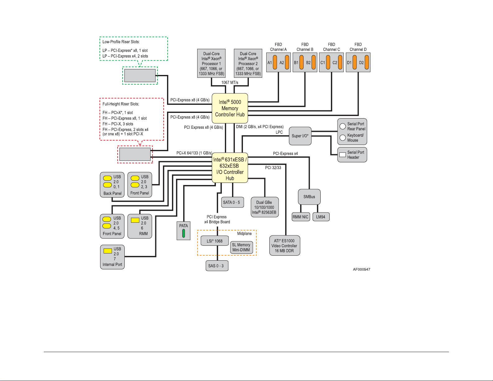
Figure 1. Intel® 5000 MCH Functional Architechture
Revision 1.1
3
Intel order number D38960-004
Page 18

Functional Architecture Intel® 5000 Series Chipsets Server Board Family Datasheet
2.1 Intel® 5000 MCH Components
The chipsets consist of two components that together are responsible for providing the interface
between all major sub-systems found on the Intel
®
server or workstation board. These sub-
systems include the processor, memory, and I/O sub-systems. These components are:
Intel
Intel
®
5000 Memory Controller Hub (Intel® 5000 MCH)
®
Enterprise South Bridge 2 (Intel® 631xESB / 632xESB I/O Controller Hub)
The following sub-sections provide an overview of the primary functions and supported features
of each chipset component used on the Intel
®
boards that utilize the Intel® 5000 MCH. Later
sections in this chapter provide more detail on how each sub-system is implemented.
Note: See the Intel
®
server board or workstation board technical product specification that
applies to your product for feature-specific support information.
2.1.1 Memory Controller Hub (Intel® 5000 MCH)
The Intel® 5000 MCH is a 1432-ball FC-BGA package configured to support the following
interfaces:
CPU dual, independent system bus at 667-, 1066-, or 1333-MHz operation.
Four fully-buffered DIMM (FBD) channels supporting fully-buffered DDR2 DIMMs
(FBDIMMs), 24-lane serial bus at 6.4 GB/s (533 MT/s) and 8 GB/s (667 MT/s) peak
theoretical bandwidth per channel. This allows a total of 25.6 GB/s and 64.6 GB/s peak
theoretical bandwidth for all four Channels combined.
One PCI Express* x8 port with an aggregate bandwidth of 4 GB/s interface to the Intel®
631xESB / 632xESB I/O Controller Hub.
One PCI Express x8 port with an aggregate bandwidth of 4 GB/s interface to x8 PCI
Express Connector.
One PCI Express x8 port with an aggregate bandwidth of 4 GB/s interface to x8 PCI
Express Connector.
One PCI Express x4 ESI port with an aggregate bandwidth of 2 GB/s interface to the
Intel® 631xESB / 632xESB I/O Controller Hub.
2.1.1.1 System Bus
The Intel
Xeon
system bus frequency of 266 MHz and 333 MHz for Intel
®
5000 MCH supports either single- or dual-processor configurations using the Intel®
®
5000 Sequence processor with a 2x 2 MB cache. The Intel® 5000 MCH supports a base
®
5000 Series Chipsets. The address
and request interface is double-pumped to 533 MHz, and the 64-bit data interface (+ parity) is
quad-pumped to 1066 MHz. This provides a matched system bus address and data bandwidths
of 8.5 GB/s.
Revision 1.1
4
Intel order number D38960-004
Page 19

Intel® 5000 Series Chipsets Server Board Family Datasheet Functional Architecture
®
2.1.1.2 Intel
®
The Intel
5000 MCH provides an integrated memory controller for direct connection to four
5000 MCH Memory Sub-System Overview
channels of registered fully-buffered DIMM (FBD) DDR2 533/667 MHz memory (stacked or
unstacked). Peak theoretical memory data bandwidth using FBD 533/667 MHz technology is 6.4
and 8 GB/s, respectively.
When all four memory channels are populated and operating, they function in lock-step mode.
The maximum supported FBD DDR2 533/667 MHz memory configuration is 64 GB.
The Intel
®
5000 MCH memory interface provides several reliability, availability, serviceability,
usability, and manageability (RASUM) features, including:
Memory mirroring allows two copies of all data in the memory subsystem (one on each
channel) to be maintained.
Memory sparing allows one DIMM per channel to be held in reserve and brought on-line
if another FBDIMM in the channel becomes defective.
Hardware periodic memory scrubbing, including demand scrub support.
Retry on uncorrectable memory errors.
Intel
®
x4/x8 Single Device Data Correction (SDDC) for memory error detection and
correction of any number of bit failures in a single x4/x8 memory device.
Note: Memory sparing and memory mirroring are mutually exclusive.
Note: Memory sparing and mirroring features are currently disabled and will be made available
after production launch.
2.1.1.3 PCI Express* Interface
®
The Intel
bandwidth. The scalable PCI Express interface of the Intel
5000 MCH supports the PCI Express* high-speed serial I/O interface for superior I/O
®
5000 MCH complies with the PCI
Express Interface Specification, Revision 1.0a.
The Intel
®
5000 MCH provides three x8 PCI Express* interfaces, each with a maximum
theoretical bandwidth of 4.2 GB/s. Each of these x8 PCI Express interfaces may alternatively be
configured as two independent x4 PCI Express interfaces. A PCI Express interface/port is
defined as a collection of lanes. Each lane (x1) consists of two striped differential pairs in each
direction (transmit and receive). The raw bit-rate on the data pins of 2.5 Gb/s, results in a real
bandwidth of 250 MB/s per pair, given the 8/10 bit encoding used to transmit data across this
interface.
The Intel
Specification. The PCI Express* interfaces of the Intel
®
5000 MCH is a root-class component as defined in the PCI Express Interface
®
5000 MCH support connections to a
variety of bridges and devices that are compliant with the same revision of the specification.
Revision 1.1
Intel order number D38960-004
5
Page 20

Functional Architecture Intel® 5000 Series Chipsets Server Board Family Datasheet
2.1.1.3.1 PCI Express* Training
To establish a connection between PCI Express* endpoints, the endpoints participate in a
sequence of steps called training. This sequence establishes the operational width of the link
and adjusts skews of the various lanes within a link so that the data sample points can correctly
take a data sample from the link.
In the case of a x8 port, the x4 link-pairs first attempt to train independently, and will collapse to
a single link at the x8 width upon detection of a single device returning link ID information
upstream. Once the number of links has been established, they negotiate to train at the highest
common width, and step down in its supported link widths to succeed in training. The result may
be that the link has trained as a x1 link.
Although the bandwidth of this link size is substantially lower than a x8 link or a x4 link, it allows
communication between the two devices. Software can then interrogate the device at the other
end of the link to determine why it failed to train at a higher width. This would not be possible
without support for the x1 link width.
Width negotiation is done only during training or retraining, not during recovery.
2.1.1.3.2 PCI Express* Retry
The PCI Express* interface incorporates a link-level retry mechanism. The hardware detects a
corrupted transmission packet and performs a retry of that packet and all following packets.
Although this causes a temporary interruption in the delivery of packets, the retry helps to
maintain the link integrity.
2.1.1.3.3 PCI Express* Link Recovery
If excessive errors occur, the hardware can determine that the quality of the connection is in
question and the end points can enter a quick training sequence, known as recovery. The width
of the connection will not be renegotiated, but the adjustment of skew between lanes of the link
might occur. This occurs without any software intervention, but the software might be notified.
2.1.1.3.4 PCI Express* Data Protection
The PCI Express* high-speed serial interface uses traditional CRC protection. The data packets
use a 32-bit CRC protection scheme, the same CRC-32 used by Ethernet. The smaller link
packets use a 16-bit CRC scheme. Since packets utilize 8B/10B encoding, and not all
encodings are used; this provides further data protection, as illegal codes can be detected. If
errors are detected on the reception of data packets due to various transients, these data
packets can be retransmitted. Hardware logic supports this link-level retry without software
intervention.
Revision 1.1
6
Intel order number D38960-004
Page 21

Intel® 5000 Series Chipsets Server Board Family Datasheet Functional Architecture
2.1.1.3.5 PCI Express* Retrain
If the hardware is unable to perform a successful recovery, then the link automatically reverts to
the polling state and initiates a full retraining sequence. This is a drastic event with an implicit
reset to the downstream device and all subordinate devices, and is logged by the Intel
®
5000
MCH as a "Link Down" error. If escalation of this event is enabled, software is notified of the link
DL_DOWN condition. If software is involved, then data is probably lost, and processes need to
be restarted. This is preferred over the taking down the system or going offline for an extended
time.
2.1.1.4 Enterprise South Bridge Interface (ESI)
A PCI interface is provided for a connection to the memory controller hub (Intel
®
5000 MCH).
Maximum realized bandwidth on this interface is 2 GB/s in each direction simultaneously, for an
aggregate of 4 GB/s. This PCI Express* interface is compliant with the PCI Express Base
Specification Revision 1.0a, and supports x4 and x8 bandwidths.
2.1.2 Intel® 631xESB / 632xESB I/O Controller Hub (ESB2)
The Intel® 631xESB / 632xESB I/O Controller Hub is a multi-function device that provides an
upstream hub interface for access to several embedded I/O functions and features, including:
Compliant with the PCI Express Base Specification, Revision 1.0a, with support for four
PCI Express* root ports (module-based hot-plug support) and two 1x4 downstream ports
(connector-based hot-swap support)
Compliant with the PCI-X Addendum to the PCI Local Bus Specification, Revision 1.0b
Compliant with the PCI Local Bus Specification, Revision 2.3 with support for 33 MHz
PCI operations
Compliant with the PCI Standard Hot-Plug Controller and Subsystem Specification,
Revision 1.0
ACPI 2.0 power management logic support
Enhanced DMA controller, interrupt controller, and timer functions
Integrated IDE controller with support for Ultra ATA100 / 66 / 33
Integrated SATA controller
Baseboard management controller (BMC)
USB host interface with support for eight USB 2.0 ports; via four UHCI host controllers;
and one EHCI high-speed host controller
Compliant with the System Management Bus (SMBus) Specification, Version 2.0 with
additional support for I
Support for the Audio Codec ‘97, Revision 2.3 Specification
Low pin count (LPC) interface
2
C devices
Each function within the Intel
®
631xESB / 632xESB I/O Controller Hub has its own set of
configuration registers. Once configured, each appears to the system as a distinct hardware
controller that shares the same PCI bus interface.
Revision 1.1
Intel order number D38960-004
7
Page 22

Functional Architecture Intel® 5000 Series Chipsets Server Board Family Datasheet
2.1.2.1 PCI Interface
®
The Intel
2.3-compliant implementation. All PCI signals are 5-V tolerant, except for PME#. An integrated
PCI arbiter supports up to six external PCI bus masters in addition to the internal Intel
631xESB / 632xESB I/O Controller Hub requests. On Intel
631xESB / 632xESB I/O Controller Hub PCI interface supports a 33-MHz, Revision
®
®
boards that use the Intel® 5000
MCH, this PCI interface is used to support one on-board PCI device: the ATI* ES1000 video
controller.
2.1.2.2 PCI Express* Interface
The Intel
®
631xESB / 632xESB I/O Controller Hub provides PCI Express* root ports that are
compliant with the PCI Express Base Specification Revision 1.0a. The PCI Express root ports
can be statically configured as four x1 ports or ganged together to form one x4 port. Each root
port supports 250 MB/s bandwidth in each direction (500 MB/s concurrent).
The Intel
®
631xESB / 632xESB I/O Controller Hub implements two x4 downstream ports. The
maximum realized bandwidth on this interface is 1 GB/s in each direction simultaneously, for an
aggregate of 2 GB/s. These two ports can be configured as one x8 PCI Express* port. This PCI
Express interface is compliant with the PCI Express Base Specification Revision 1.0a.
2.1.2.3 PCI-X* Bus Interface
The Intel
conventional PCI and PCI-X Mode 1. The PCI-X interfaces on the Intel
®
631xESB / 632xESB I/O Controller Hub provides a PCI-X* bus interface that supports
®
631xESB / 632xESB
I/O Controller Hub are compliant with the following:
“PCI-X Addendum” to the PCI Local Bus Specification Revision 1.0b
“Mode 1” sections of the “PCI-X Electrical and Mechanical Addendum” to the PCI Local
Bus Specification Revision 2.0a
“PCI-X Protocol Addendum” to the PCI Local Bus Specification Revision 2.0a
The Intel
®
631xESB / 632xESB I/O Controller Hub supports PCI bus frequencies of 66 MHz,
100 MHz, and 133 MHz.
2.1.2.4 IDE Interface (Bus Master Capability and Synchronous DMA Mode)
The Intel
®
631xESB / 632xESB I/O Controller Hub has an integrated IDE controller with an
independent IDE signal channel that supports up to two IDE devices. This integrated
functionality provides the interface for IDE hard disks and ATAPI devices. Each IDE device can
have independent timings. The IDE interface supports PIO IDE transfers of up to 16 MB/s and
Ultra ATA transfers of up 100 MB/s. The IDE interface integrates 16x32-bit buffers for optimal
transfers and does not consume any ISA DMA resources. The IDE signal channels in the Intel
®
631xESB / 632xESB I/O Controller Hub can be configured to primary and secondary channels.
Revision 1.1
8
Intel order number D38960-004
Page 23

Intel® 5000 Series Chipsets Server Board Family Datasheet Functional Architecture
2.1.2.5 Serial ATA (SATA) Host Controller
The SATA host controller supports a combination of up to six SATA or four serial attached SCSI
(SAS) devices. This provides an interface for SATA hard disks and ATAPI devices. The SATA
interface supports PIO IDE transfers up to 16 MB/s and Serial ATA transfers up to 3.0 Gb/s (300
MB/s).
The SATA system for the Intel
®
631xESB / 632xESB I/O Controller Hub contains six
independent SATA signal ports that can be independently electrically isolated. Each SATA
device can have independent timings. They can be configured to the standard primary and
secondary channels. In addition, the controller hub offers the Intel
®
Embedded Server RAID
Technology that enables data striping (RAID Level 0) for higher-performance or data mirroring
(RAID Level 1) for fault-tolerance between the two SATA drives, alleviating disk bottlenecks by
taking advantage of the dual, independent SATA controllers integrated in the Intel
®
631xESB /
632xESB I/O Controller Hub.
Note: See the Intel
®
server board or workstation board technical product specification that
applies to your product for more information.
2.1.2.6 Baseboard Management Controller (BMC)
®
The BMC component of the Intel
631xESB / 632xESB I/O Controller Hub is provided by an
embedded ARC* controller and associated peripheral functionality that is used to provide the
baseboard management controller functionality that is required for IPMI-based server
management. The following is a summary of the Intel
®
631xESB / 632xESB I/O Controller Hub
management hardware features utilized by the BMC:
ARC4 processor with 16 Kb I-cache and D-cache
256 Kb of internal SRAM with dual port (one for code accesses and one for all other
accesses).
Expansion bus, allowing connection to external Flash PROM (asynchronous or
synchronous), an external SRAM or an external SDRAM.
Serial flash interface
Five SMB ports, two that support FML (either master or slave)
RS-232 serial port (UART)
Cryptographic module, supporting AES and RC4 encryption algorithms and SHA1 and
MD5 authentication algorithms with internal DMA and raw checksum support.
Two keyboard controller style (KCS) interfaces residing on the LPC bus
General-purpose input/output (GPIO) interface
MAC CSR interface
Timer interface
Host DMA interface
Revision 1.1
Intel order number D38960-004
9
Page 24

Functional Architecture Intel® 5000 Series Chipsets Server Board Family Datasheet
2.1.2.7 Low Pin Count (LPC) Interface
®
The Intel
the Low Pin Count Interface Specification, Revision 1.1. The low pin count (LPC) bridge function
of the Intel
631xESB / 632xESB I/O Controller Hub implements an LPC Interface as described in
®
631xESB / 632xESB I/O Controller Hub resides in PCI Device 31: Function 0. In
addition to the LPC bridge interface function, D31:F0 contains other functional units including
DMA, interrupt controllers, timers, power management, system management, GPIO, and RTC.
2.1.2.8 Compatibility Modules (DMA Controller, Timer/Counters, Interrupt
Controller)
The DMA controller incorporates the logic of two 82C37 DMA controllers, with seven
independently programmable channels. Channels 0–3 are hardwired to 8-bit, count-by-byte
transfers, and channels 5 through 7 are hardwired to 16-bit, count-by-word transfers. Any two of
the seven DMA channels can be programmed to support fast Type-F transfers.
The Intel
DMA use the Intel
®
631xESB / 632xESB I/O Controller Hub supports LPC DMA. LPC DMA and PC/PCI
®
631xESB / 632xESB I/O Controller Hub’s DMA controller. LPC DMA is
handled through the use of the LDRQ# lines from peripherals and special encoding on LAD[3:0]
from the host. Single, demand, verify, and increment modes are supported on the LPC
interface. Channels 0–3 are 8 bit channels. Channels 5 through 7 are 16-bit channels. Channel
4 is reserved as a generic bus master request.
The timer / counter block contains three counters that are equivalent in function to those found
in one 82C54 programmable interval timer. These three counters are combined to provide the
system timer function, and speaker tone. The 14.31818-MHz oscillator input provides the clock
source for these three counters.
The Intel
®
631xESB / 632xESB I/O Controller Hub provides an ISA-compatible programmable
interrupt controller (PIC) that incorporates the functionality of two 82C59 interrupt controllers.
The two interrupt controllers are cascaded so that 14 external and two internal interrupts are
possible. In addition, the I/O Controller Hub supports a serial interrupt scheme. All of the
registers in these modules can be read and restored. This is required to save and restore the
system state after power has been removed and restored to the platform.
2.1.2.9 Advanced Programmable Interrupt Controller (APIC)
In addition to the standard ISA-compatible PIC described in the previous section, the Intel
®
631xESB / 632xESB I/O Controller Hub incorporates the Advanced Programmable Interrupt
Controller (APIC).
2.1.2.10 Universal Serial Bus (USB) Controller
The Intel
®
631xESB / 632xESB I/O Controller Hub contains an enhanced host controller
interface that supports USB high-speed signaling. High-speed USB 2.0 allows data transfers up
to 480 Mb/s, which is 40 times faster than full-speed USB. The I/O Controller Hub also contains
four universal host controller interface (UHCI) controllers that support USB full-speed and lowspeed signaling.
The Intel
®
631xESB / 632xESB I/O Controller Hub supports eight USB 2.0 ports. All eight ports
capable of high-speed, full-speed, and low-speed.
Revision 1.1
10
Intel order number D38960-004
Page 25

Intel® 5000 Series Chipsets Server Board Family Datasheet Functional Architecture
2.1.2.11 Real-time Clock (RTC)
®
The Intel
631xESB / 632xESB I/O Controller Hub contains a Motorola* MC146818A-compatible
real-time clock with 256 bytes of battery-backed RAM. The real-time clock performs two key
functions: keeping track of the time of day and storing system data, even when the system is
powered down. The RTC operates on a 32.768-KHz crystal and a separate 3-V lithium battery.
The RTC supports two lockable memory ranges. By setting bits in the configuration space, two
8-byte ranges can be locked to read and write accesses. This prevents unauthorized reading of
passwords or other system security information.
2.1.2.12 General-purpose Input/Output (GPIO)
General-purpose inputs and outputs are provided for custom system designs. The number of
inputs and outputs depends on the Intel
®
631xESB / 632xESB I/O Controller Hub configuration.
All unused GPI pins must be pulled high or low, so they are at a predefined level and do not
cause problems.
Note: See the Intel
®
server board or workstation board technical product specification that
applies to your product for more information.
2.1.2.13 System Management Bus (SMBus 2.0)
®
The Intel
the processor to communicate with SMBus slaves. This interface is compatible with most I
devices. Special I
631xESB / 632xESB I/O Controller Hub contains a SMBus host interface that allows
2
C commands are implemented. The SMBus host controller for the I/O
2
C
Controller Hub provides a mechanism for the processor to initiate communications with SMBus
peripherals (slaves).
The Intel
®
631xESB / 632xESB I/O Controller Hub supports slave functionality, including the
Host Notify protocol. The host controller supports eight command protocols of the SMBus
interface: Quick Command, Send Byte, Receive Byte, Write Byte/Word, Read Byte/Word,
Process Call, Block Read/Write, and Host Notify.
See the System Management Bus (SMBus) Specification, Version 2.0 for more information.
2.2 Processor Sub-system
The support circuitry for the processor sub-system consists of the following:
Dual LGA771 zero insertion force (ZIF) processor sockets
Processor host bus AGTL+ support circuitry
Reset configuration logic
Processor module presence detection logic
BSEL detection capabilities
CPU signal level translation
Common enabling kit (CEK) CPU retention support
Revision 1.1
Intel order number D38960-004
11
Page 26

Functional Architecture Intel® 5000 Series Chipsets Server Board Family Datasheet
2.2.1 Processor Support
Intel® boards that use the Intel® 5000 MCH support one or two Intel® Xeon® 5000 sequence
processors that utilize a 667, 1066, or 1333 MHz system bus with frequencies starting at 3.67
GHz. Previous generations of the Intel
®
Xeon® processors are not supported on these boards.
2.2.2 Processor Population Rules
When two processors are installed, both must be of identical revision, core voltage, and
bus/core speed. When only one processor is installed, it must be in the socket labeled CPU1.
The other socket must be empty.
Processors must be populated in sequential order. Processor socket 1 (CPU1) must be
populated before processor socket 2 (CPU2). No terminator is required in the second processor
socket when using a single processor configuration.
The board is designed to provide up to 130 A of current per processor. Processors with higher
current requirements are not supported.
2.2.3 Processor EVRD
EVRD11.0, Enterprise Voltage Regulator Down, is a DC-to-DC converter that meets the
processor power requirements server platform. Processors supported by this VR are: Intel
®
5000 sequence processors and future processor technologies
EVRD11.0 incorporates functional changes from prior EVRD design guidelines.
2.2.4 GTL2007
The GTL2007 is a customized translator between dual Intel® Xeon® 5000 sequence processors,
system health management, Intel
LVTTL and GTL signals. The GTL2007 is a 12-bit translator to interface between the 3.3-V
LVTTL chipset I/O and the Dual-Core Intel
GTL / GTL+ I/O. The device is designed for platform health management in dual-processor
applications.
®
631xESB / 632xESB I/O Controller Hub, and power supply
®
Xeon® 5000 processor sequence processor GTL- /
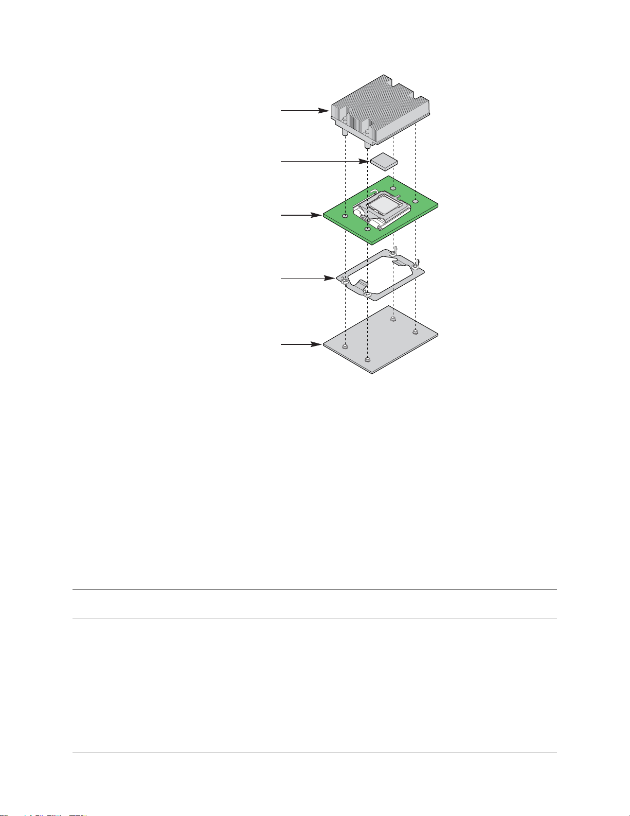
2.2.5 Common Enabling Kit (CEK) Design Support
The Intel® board complies with the Intel® Common Enabling Kit (CEK) processor mounting and
thermal solution. The server board ships from Intel’s factory with a CEK spring snapped onto the
underside of the board beneath each processor socket. The CEK spring is removable to allow
the use of non-Intel heat sink retention solutions.
Revision 1.1
12
Intel order number D38960-004
Page 27
Intel® 5000 Series Chipsets Server Board Family Datasheet Functional Architecture
Heatsink assembly
Thermal Interface
Material (TIM)
Server Board
CEK Spring
Chassis
Figure 2. CEK Processor Mounting
TP02091
AF000196
2.3 Memory Sub-system
The Intel® boards that use the Intel® 5000 MCH support several fully-buffered (FBD) memory
modes of operation.
Single-channel mode (single DIMM mode)
Single-branch / dual-channel mode
Dual-branch / dual-channel mode (four channels)
Memory sparing mode
Memory mirroring mode
Note: Memory sparing and mirroring features are currently disabled and will be made available
after production launch.
The Intel® 5000 MCH provides an integrated memory controller for direct connection to four
channels routed to eight connectors supporting registered DDR2-533 and DDR2-667 FBDIMM
memory (stacked or unstacked). Peak theoretical memory data bandwidth is 6.4 GB/s with
DDR2-533 and 8.0 GB/s with DDR2-667.
A pair of channels is a branch. Branch 0 consists of channel A and channel B, Branch 1
consists of channel C and channel D. A DIMM can have two ranks; a channel supports a
maximum of eight ranks.
Revision 1.1
Intel order number D38960-004
13
Page 28

Functional Architecture Intel® 5000 Series Chipsets Server Board Family Datasheet
In non-mirrored operation, the two DDR2 channels within a branch operate in lock-step and the
branches operate independently. When memory mirroring is configured, the channels operate in
lock-step under normal conditions, but independently under failure and recovery conditions.
The Intel
®
5000 MCH supports a burst length of four in either single-channel mode or dualchannel mode. In dual-channel mode this results in eight 64-bit chunks (64-byte cache line)
from a single read or write. In single-channel mode, two reads or writes are required to access a
cache line of data.
Memory between 32 GB, and 32 GB minus 512 MB, is not accessible for use by the operating
system and may be lost to the user. This area is reserved for the BIOS, APIC configuration
space, PCI adapter interface, and virtual video memory space. This means that if 32 GB of
memory is installed, 31.5 GB of this memory is usable. The chipset should allow the remapping
of unused memory above the 32 GB address, but this memory may not be accessible to an
operating system that has a 32 GB memory limit.
To boot the system, the system BIOS uses a dedicated I
needed to program the Intel
®
5000 MCH memory registers.
2
C bus to retrieve DIMM information
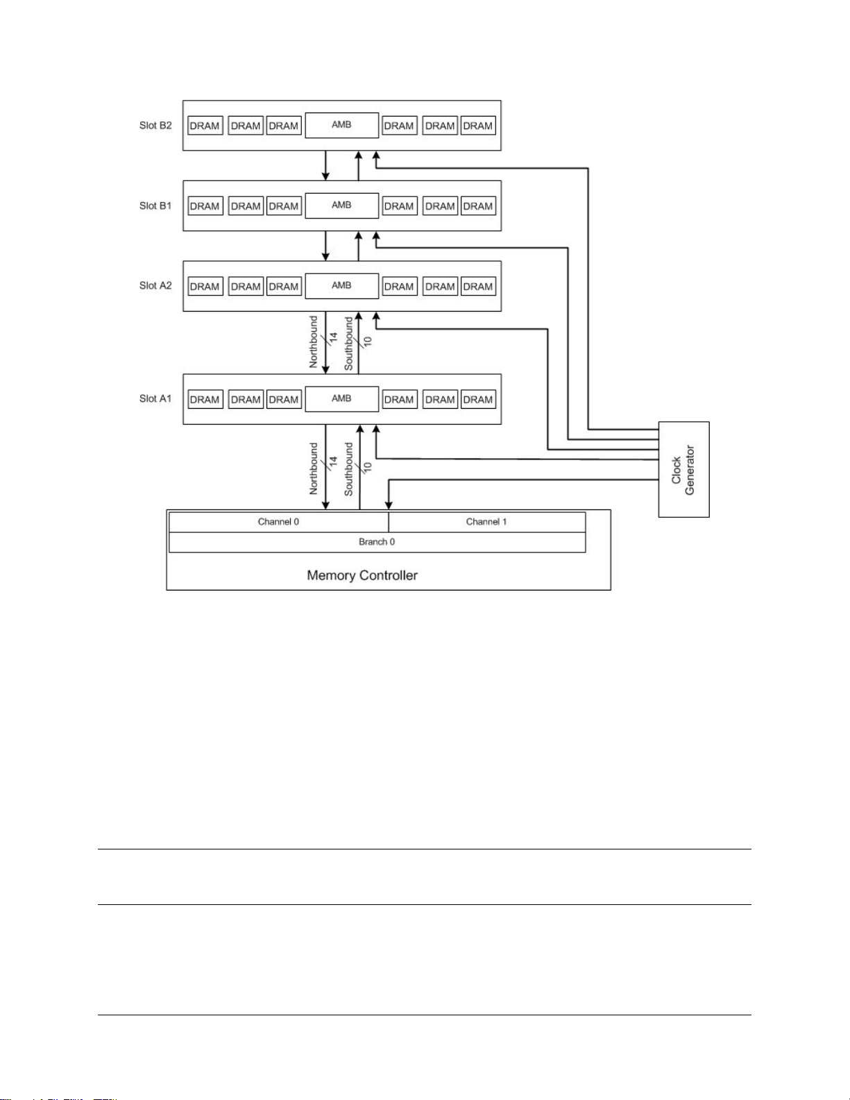
2.3.1 Fully-buffered DIMM (FBDIMM)
The fully-buffered DIMM (FBDIMM) memory interface provides a high-bandwidth, large-capacity
channel solution that has a narrow host interface. FBDIMMs use commodity DRAMs isolated
from the channel behind an advanced memory buffer (AMB) on the DIMM that allows a greater
number of devices per channel without loading the interconnect and affecting performance.
Memory capacity remains at a maximum of 36 devices per DIMM and total memory capacity
scales with DRAM bit density.
FBD is a differential pair, point-to-point interface. The interface consists primarily of 10
southbound differential pairs (outputs from the Intel
northbound differential pairs (inputs to the Intel
®
5000 MCH to the DIMMs) and 14
®
5000 MCH from the DIMMs). The Intel® 5000
MCH is connected only to the closest FBDIMM in the channel and communicates with the AMB
on that FBDIMM. The AMB on the closest FBDIMM communicates with the AMB on the next
FBDIMM in the channel, and so on. This point-to-point solution eliminates problems associated
with a “stub-bus” architecture and allows memory capacity to increase without loading the
channel. The figure below shows the FBD topology.
Revision 1.1
14
Intel order number D38960-004
Page 29
Intel® 5000 Series Chipsets Server Board Family Datasheet Functional Architecture
Figure 3. FBD Topology
2.3.2 Supported Memory
The Intel® 5000 MCH supports single-channel DIMM operation in which only one FBDIMM is
installed in DIMM socket A1. Population in other DIMM banks is not supported for singlechannel operation.
The server and workstation boards provide the maximum memory capacities outlined in
Table 1, based on the number of DIMM slots provided and maximum supported memory loads
by the chipset. The minimum memory supported with the system running in single-channel
memory mode is 512 MB, using a single DIMM in the DIMM A1 socket.
Note: All Intel memory qualification is done by testing with complete memory banks of identical
memory modules in all DIMM sockets. Memory qualification does not include testing of singlechannel memory mode, mixed DIMM type and/or vendors.
Supported DIMM capacities are 512 MB, 1 GB, 2 GB, and 4 GB.
Revision 1.1
Intel order number D38960-004
15
Page 30
Functional Architecture Intel® 5000 Series Chipsets Server Board Family Datasheet
Table 1. DIMM Module Capacities
SDRAM Parts / SDRAM Technology Used 512Mb 1Gb 2Gb 4Gb
X8, single row 512MB 1GB 2GB 4GB
X8, double row 1GB 2GB 4GB 8GB
X4, single row 512MB 1GB 2GB 4GB
X4, Stacked, double row 1GB 2GB 4GB 8GB
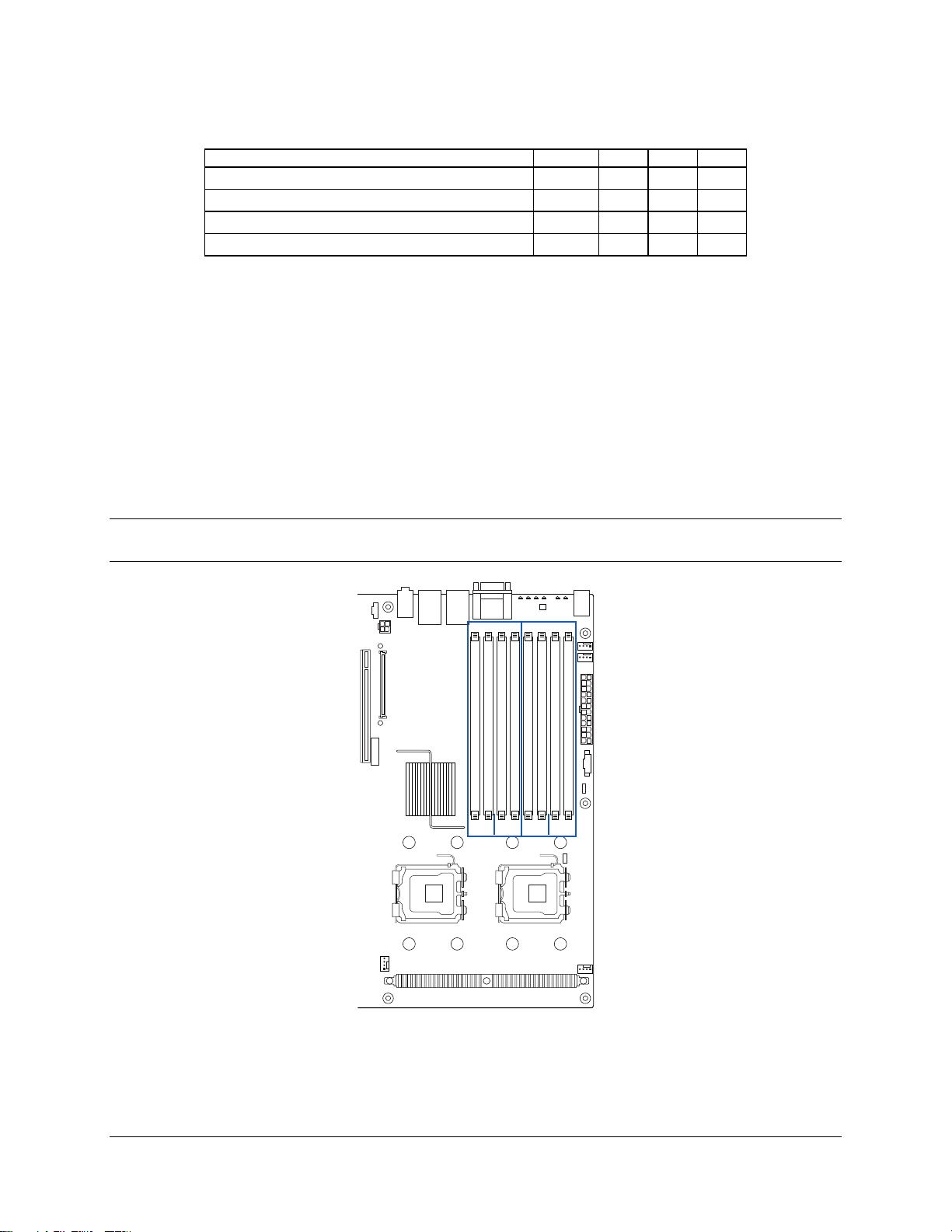
DIMMs on channel A are paired with DIMMs on channel B to configure 4-way interleaving. Each
DIMM pair is referred to as a bank. The bank can be further divided into two rows, based on
single-sided or double-sided DIMMs. If both DIMMs in a bank are single-sided, only one row is
said to be present. For double-sided DIMMs, both rows are said to be present.
The server and workstation boards have eight DIMM slots, or four DIMM channels. Both DIMMs
in a channel should be identical (same manufacturer, CAS latency, number of rows, columns
and devices, timing parameters, etc.). Although DIMMs within a channel must be identical, the
BIOS supports various DIMM sizes and configurations, allowing the channels of memory to be
different. Memory sizing and configuration is guaranteed only for qualified DIMMs approved by
Intel.
Note: Some boards vary in memory capacity. See the server or workstation Technical Product
Specification that applies to your product for more information.
Branch 1 Branch 2
DIMM A1
DIMM A2
DIMM B1
DIMM B2
DIMM C1
DIMM C2
DIMM D1
DIMM D2
Ch 1 Ch 2 Ch 3 Ch 4
AF000169
Figure 4. Identifying Banks of Memory
Revision 1.1
16
Intel order number D38960-004
Page 31

Intel® 5000 Series Chipsets Server Board Family Datasheet Functional Architecture
2.4 I/O Sub-system
The I/O sub-system consists of several components:
PCI sub-system
Serial ATA (SATA) support
Serial-attached SCSI (SAS)
RAID support
Parallel ATA (PATA) support
Video controller
Network interface controller (NIC)
USB 2.0 support
Super I/O support
This section describes the function of each I/O interface and how they operate.
2.4.1 PCI Sub-system
2.4.2 Scan Order
The BIOS assigns PCI bus numbers in a depth-first hierarchy, in accordance with the PCI Local
Bus Specification, Revision 2.2. The bus number is incremented when BIOS locates a bridge
device that is not part of the chipset. Scanning continues on the secondary side of the bridge
until all subordinate buses are assigned numbers. PCI bus number assignments may vary from
boot to boot with varying presence of PCI devices with PCI-PCI bridges. If a device with a
bridge with a single bus behind it is inserted into a PCI bus, all subsequent PCI bus numbers
below the current bus are increased by one.
The bus assignments occur once, early in the BIOS boot process, and never change during the
pre-boot phase.
2.4.3 Resource Assignment
The BIOS resource manager assigns the PIC-mode interrupt for the devices that are accessed
by the legacy code. The BIOS will ensure the PCI BAR registers and the command register for
all devices are correctly set up to match the behavior of the legacy BIOS after booting to a
legacy operating system. Any legacy code cannot make any assumption about the scan order of
devices or the order in which resources are allocated to them.
In legacy mode, the BIOS supports the INT 1Ah PCI BIOS interface calls.
2.4.4 Automatic IRQ Assignment
The BIOS automatically assigns IRQs to devices in the system for legacy compatibility. No
method is provided to manually configure the IRQs for devices.
Revision 1.1
Intel order number D38960-004
17
Page 32

Functional Architecture Intel® 5000 Series Chipsets Server Board Family Datasheet
2.4.5 Legacy Option ROM Support
The legacy support code in the BIOS will dispatch the legacy option ROMs in the available
memory space in the address range 0C0000h-0DFFFFh and will follow all the legacy rules with
respect to the option ROM space. If room is available in the E segment, and both C and D
segments are already used, the BIOS will also shadow up to 0E7FFF. The BIOS allows the user
to disable the shadowing of the onboard PCI devices.
2.4.6 EFI PCI APIs
The BIOS provides standard PCI protocols as described in the Extensible Firmware Interface
Reference Specification, Version 1.1.
2.4.7 Legacy PCI APIs
In legacy mode, the system BIOS will support the INT 1Ah, AH = B1h functions as defined in the
PCI BIOS Specification, Revision 2.1. The system BIOS supports the real mode interface.
2.4.8 Dual Video
The BIOS supports single and dual video modes. Dual video mode is disabled by default.
In single video mode, the onboard video controller is disabled when an add-in video card
is detected.
In dual video mode, the onboard video controller is enabled and is the primary video
device. The external video card is allocated resources and is considered the secondary
video device.
See the server or workstation Technical Product Specification that applies to your product for
more information.
2.4.9 Parallel ATA (PATA) Support
The integrated IDE controller of the Intel® 631xESB / 632xESB I/O Controller Hub ICH6
provides one IDE channel. This IDE channel can support one optical drive. The IDE channels
can be configured and enabled or disabled by accessing the BIOS Setup Utility during POST.
The BIOS supports the ATA/ATAPI Specification, version 6. It initializes the embedded IDE
controller in the chipset south-bridge and the IDE devices that are connected to these devices.
The BIOS scans the IDE devices and programs the controller and the devices with their
optimum timings. The IDE disk read/write services that are provided by the BIOS use PIO
mode, but the BIOS will program the necessary Ultra DMA registers in the IDE controller so that
the operating system can use the Ultra DMA modes.
The BIOS initializes and supports ATAPI devices such as LS-120/240, CD-ROM, CD-RW, and
DVD-ROM drives.
Revision 1.1
18
Intel order number D38960-004
Page 33

Intel® 5000 Series Chipsets Server Board Family Datasheet Functional Architecture
2.4.9.1 Ultra ATA/100
®
The IDE interface of the Intel
631xESB / 632xESB I/O Controller Hub ICH DMA protocol
redefines signals on the IDE cable to allow both host and target throttling of data and transfer
rates of up to 100 MB/s.
2.4.9.2 IDE Initialization
The BIOS supports the ATA/ATAPI Specification, version 6. The BIOS initializes the embedded
IDE controller in the chipset (Intel
®
631xESB / 632xESB I/O Controller Hub) and the IDE device
that is connected to this device. The BIOS scans the IDE device and programs the controller
and the device with their optimum timings. The IDE disk read/write services that are provided by
the BIOS use PIO mode, but the BIOS programs the necessary Ultra DMA registers in the IDE
controller so the operating system can use the Ultra DMA modes.
2.4.10 Serial ATA (SATA) Support
The integrated Serial ATA (SATA) controller of the Intel® 631xESB / 632xESB I/O Controller
Hub provides up to six SATA or four SAS devices ports on the server board. The SATA ports
can be enabled / disabled and/or configured through the BIOS Setup Utility.
The BIOS initializes and supports SATA devices just like PATA devices. It initializes the
embedded IDE controllers in the chipset and any SATA devices that are connected to these
controllers. From a software standpoint, SATA controllers present the same register interface as
PATA controllers. Hot-plugging SATA drives during the boot process is not supported by the
BIOS and may result in undefined behavior.
The SATA function in the Intel
operation to support different operating system conditions. In the case of native IDE-enabled
operating systems, the Intel
functions for serial and parallel ATA. To support legacy operating systems, there is only one PCI
function for both the serial and parallel ATA ports.
®
631xESB / 632xESB I/O Controller Hub has dual modes of
®
631xESB / 632xESB I/O Controller Hub has separate PCI
The MAP register provides the ability to share PCI functions. When sharing is enabled, all I/O
decoding is done through the SATA registers. A software write to the Function Disable Register
(D31, F0, offset F2h, bit 1) causes Device 31, Function 1 (IDE controller) to be hidden and its
configuration registers are not used. The SATA Capability Pointer Register (offset 34h) will
change to indicate that Message Signaled Interrupt (MSI) is not supported in combined mode.
The Intel
signals that can be independently enabled or disabled. Each interface is supported by an
independent DMA controller. The Intel
®
631xESB / 632xESB I/O Controller Hub SATA controller features two sets of interface
®
631xESB / 632xESB I/O Controller Hub SATA controller
interacts with an attached mass storage device through a register interface that is equivalent to
that which is presented by a traditional IDE host adapter. The host software follows existing
standards and conventions when accessing the register interface and follows standard
command protocol conventions.
SATA interface transfer rates are independent of UDMA mode settings. SATA interface transfer
rates will operate at the bus’s maximum speed, regardless of the UDMA mode reported by the
SATA device or the system BIOS.
Revision 1.1
Intel order number D38960-004
19
Page 34

Functional Architecture Intel® 5000 Series Chipsets Server Board Family Datasheet
2.4.11 SATA RAID Functionality
See the server or workstation Technical Product Specification that applies to your product for
information.
2.4.12 Serial Attached SCSI
See the server or workstation Technical Product Specification that applies to your product for
information.
2.4.13 Video Controller
See the server or workstation Technical Product Specification that applies to your product for
information.
2.4.14 Network Interface Controller (NIC)
The Intel® server boards that use this chipset supports two 10Base-T / 100Base / 1000Base-T
network interface controllers (NIC) based on the Intel
workstation boards that use this chipset support one 10Base-T / 100Base / 1000Base-T
network interface controller (NIC) based on the Intel
®
82563EB controller. The Intel®
®
82564EB controller.
Each network interface controller (NIC) drives two LED’s located on each network interface
connector. The link/activity LED (to the left of the connector) indicates network connection when
on, and Transmit/Receive activity when blinking. The speed LED (to the right of the connector)
indicates 1000-Mbps operation when amber, 100-Mbps operation when green, and 10 Mbps
when off. The table below provides an overview of the LED’s.
Table 2. NIC2 Status LED
LED Color LED State NIC State
Off 10 Mbps
Green/Amber (Left)
Green (Right)
Green 100 Mbps
Amber 1000 Mbps
On Active Connection
Blinking Transmit / Receive activity
2.4.15 USB Support
The USB controller functionality integrated into the Intel® 631xESB / 632xESB I/O Controller
Hub ICH6 provides the server board with the interface for up to eight USB 2.0 ports. One
internal USB 2.0 port is provided to support a USB internal floppy disk drive. One internal 1x10
header is provided to support an additional two optional USB 2.0 ports. USB 2.0 ports are
routed through the bridge board connector for optional front access.
Revision 1.1
20
Intel order number D38960-004
Page 35

Intel® 5000 Series Chipsets Server Board Family Datasheet Functional Architecture
2.4.16 Native USB Support
During the power on self-test (POST), the BIOS initializes and configures the USB subsystem in
accordance with chapter 14 of the Extensible Firmware Interface Reference Specification,
Version 1.1. The BIOS is capable of initializing and using the following types of USB devices:
USB Specification-compliant keyboards
USB Specification-compliant mice
USB Specification-compliant storage devices that utilize bulk-only transport mechanism
USB devices are scanned to determine if they are required for booting.
The BIOS supports USB 1.1-compliant devices and host controllers. The BIOS configures the
USB 2.0-compliant host controller and USB 2.0-compliant devices in USB 1.1 mode because all
USB 2.0 devices are required to support USB 1.1 mode. Although USB 1.1 mode is slower than
USB 2.0 mode, the difference in speed is not significant during the pre-boot phase. The
operating system can reconfigure the USB devices in USB 2.0 mode as required. The BIOS
configures the USB 2.0 host controller (EHCI) so the operating system can use it.
During the pre-boot phase, the BIOS automatically supports the hot addition and hot removal of
USB devices. For example, if a USB device is hot plugged, the BIOS detects the device
insertion, initializes the device, and makes it available to the user. Only onboard USB controllers
are initialized by BIOS. This does not prevent the operating system from supporting any
available USB controllers, including on add-in cards.
2.4.17 Legacy USB Support
The BIOS supports PS/2* emulation of USB keyboards and mice. During POST, the BIOS
initializes and configures the root hub ports and then searches for a keyboard, a mouse, and the
USB hub then enables them.
2.4.18 Super I/O
Legacy I/O support is provided by a National Semiconductor* PC87427 Super I/O device. This
chip contains the necessary circuitry to control two serial ports and PS/2-compatible keyboard
and mouse. The Intel
GPIOs
Two serial ports
Removable media drives
Keyboard and mouse support
Wake up control
System health support
®
server and workstation boards that use this chipset support the following:
Revision 1.1
Intel order number D38960-004
21
Page 36

Functional Architecture Intel® 5000 Series Chipsets Server Board Family Datasheet
2.4.18.1 General Purpose Input/Output (GPIO)
The National Semiconductor* PC87427 Super I/O provides nine general-purpose input/output
pins that the server and workstation boards utilize.
Note: See the server or workstation Technical Product Specification that applies to your product
for information.
2.4.18.2 Removable Media Drives
The BIOS supports removable media devices in accordance with the Tested Hardware and
Operating System List. The BIOS supports booting from USB mass storage devices connected
to the chassis USB port, such as a USB flash drive device. The BIOS supports USB 2.0 media
storage devices that are backward compatible to the USB 1.1 specification.
2.4.18.3 Keyboard and Mouse
Dual stacked PS/2* ports on the back edge of the server board support a keyboard and mouse.
Either port can support a mouse or keyboard. Neither port supports hot plugging, or connector
insertion, while the system is turned on.
The system can boot without a keyboard or mouse attached. If present, the BIOS will detect the
keyboard during POST and displays the message “Keyboard Detected” on the POST screen.
2.4.18.4 Wake-up Control
The Super I/O contains functionality that allows various events to control the power-on and
power-off the system.
Note See the server or workstation Technical Product Specification that applies to your product
for information.
2.4.19 BIOS Flash
The BIOS supports the Intel® 28F320C3B flash part. The flash part is a 4 MB flash ROM, of
which 2 MB is programmable. The flash ROM contains system initialization routines, a setup
utility, and runtime support routines. The layout is subject to change, as determined by Intel.
The flash ROM contains the necessary drivers for onboard peripherals such as SCSI, Ethernet,
and video controllers. The Flash Memory Update utility loads the BIOS image into the flash.
Revision 1.1
22
Intel order number D38960-004
Page 37

Intel® 5000 Series Chipsets Server Board Family Datasheet Functional Architecture
2.5 Clock Generation and Distribution
All buses on the Intel® server and workstation boards that use the Intel® 5000 MCH operate
using synchronous clocks. Clock synthesizer/driver circuitry on the server board generates
clock frequencies and voltage levels as required, including the following:
200-MHz differential clock at 0.7V logic levels. For processor 1, processor 2, debug port,
and the Intel
100-MHz differential clock at 0.7V logic levels on CK409B. For the DB800 clock buffer.
100-MHz differential clock at 0.7 Vlogic levels on DB800. For the PCI Express* device
this is the Intel
®
Intel
631xESB / 632xESB I/O Controller Hub ICH6.
66 MHz at 3.3V logic levels: for 5000 North Bridge and the Intel
®
5000 MCH.
®
5000 MCH, which includes x4 PCI Express slot. For SATA this is the
®
631xESB / 632xESB
I/O Controller Hub ICH6.
48 MHz at 3.3V logic levels: for Intel
®
631xESB / 632xESB I/O Controller Hub ICH6 and
SIO.
33 MHz at 3.3V logic levels: for the Intel
®
631xESB / 632xESB I/O Controller Hub ICH6,
video, BMC, and SIO.
14.318 MHz at 2.5V logic levels: For the Intel
®
631xESB / 632xESB I/O Controller Hub
ICH6 and video.
10 Mhz at 5V logic levels: For the BMC.
The PCI-X slot speed on the full-length riser card is determined by the riser card in use.
Revision 1.1
Intel order number D38960-004
23
Page 38

System BIOS Intel® 5000 Series Chipsets Server Board Family Datasheet
3. System BIOS
The BIOS is implemented as firmware that resides in the Flash ROM. It provides hardwarespecific initialization algorithms and standard PC-compatible basic input / output (I/O) services,
and standard Intel
embedded devices. These images are supplied by the device manufacturers and are not
specified in this document.
®
Server Board features. The Flash ROM also contains firmware for certain
The BIOS implementation is based on the Intel
®
Platform Innovation Framework for EFI
architecture and is fully compliant with all Intel Platform Innovation Framework for EFI
architecture specifications specified in the Extensible Firmware Interface Reference
Specification, Version 1.1. The Intel Platform Innovation Framework for EFI is referred to as
“Framework” in this document.
3.1 BIOS Identification String
The BIOS Identification string is used to uniquely identify the revision of the BIOS being used on
the server. The string is formatted as follows:
BoardID.OEMID.MajorRev.MinorRev.BuildID.BuildDateTime
Build Da te a n d time in
MMDDYYYYHHMM format
4 character ID
2 character ID
2 character ID
3 character ID – “86B ” = EP S D
N character ID – S 5 0 0 0PS L, etc
For example, BIOS build 3, generated on August 13, 2005 at 11:56 AM has the following BIOS
ID string that will be displayed in the POST diagnostic screen:
S5000.86B.01.00.0003.081320051156
The BIOS version in the BIOS Setup utility is displayed as:
S5000.86B.01.00.0003
Revision 1.1
24
Intel order number D38960-004
Page 39

Intel® 5000 Series Chipsets Server Board Family Datasheet System BIOS
The BIOS ID is used to identify the BIOS image. It is not used to designate either the board ID
or the BIOS phase. The board ID is available in the SMBIOS type 2 structure in which the phase
of the BIOS can be determined by the release notes associated with the image. The board ID is
also available in BIOS Setup.
3.2 Processors
3.2.1 CPUID
The following processors are supported on Intel® server boards and systems that use the Intel®
5000 Series Chipset, with their respective CPU ID:
Dual-Core Intel
Dual-Core Intel
®
Xeon® Processor 5000 sequence: CPU ID – 00000F6xh
®
Xeon® Processor 5000 sequence low voltage: CPU ID – 000006Fxh
Table 3. Supported Processor Configurations
Processor Family System Bus Speed Core Frequency Cache Watts Support
Intel® Xeon® Processor 533 MHz All No
Intel® Xeon® Processor 800 MHz All No
Intel® Xeon® Processor 5050 667 MHz 3.0 GHz 2x 2 MB 95 Yes
Intel® Xeon® Processor 5060 1066 MHz 3.2 GHz 2x 2 MB 130 Yes
Intel® Xeon® Processor 5063 1066 MHz 3.2 GHz 2x 2 MB 95 Yes
Intel® Xeon® Processor 5080 1066 MHz 3.73 GHz 2x 2 MB 130 Yes
Intel® Xeon® Processor 51xx 1333/1066 MHz TBD TBD TBD Yes
3.2.2 Multiple Processor Initialization
IA-32 processors have a microcode-based bootstrap processor (BSP) arbitration protocol. A
processor that does not perform the role of BSP is referred to as an application processor (AP).
The Intel
each of which accommodates a single Dual-Core Intel
reset, the hardware arbitration chooses one BSP from the available processor cores per system
bus. However, the BIOS power-on self-test (POST) code requires only one processor for
execution. This requires the BIOS to elect a system BSP using registers in the Intel
The BIOS cannot guarantee which processor will be the system BSP, only that a system BSP
will be selected. In the remainder of this document, the system BSP is referred to as the BSP.
®
5000 Series Chipset memory controller hub (MCH) has two processor system buses,
®
Xeon® processor 5000 sequence. At
®
5000 MCH.
The BSP is responsible for executing the BIOS POST and preparing the server to boot the
operating system. At boot time, the server is in virtual wire mode and the BSP alone is
programmed to accept local interrupts (INTR driven by programmable interrupt controller (PIC)
and non-maskable interrupt (NMI)).
Revision 1.1
Intel order number D38960-004
25
Page 40

System BIOS Intel® 5000 Series Chipsets Server Board Family Datasheet
As a part of the boot process, the BSP wakes each AP. When awakened, an AP programs its
memory type range registers (MTRRs) to be identical to those of the BSP. All APs execute a
halt instruction with their local interrupts disabled. If the BSP determines that an AP exists that
is a lower-featured processor or that has a lower value returned by the CPUID function, the BSP
switches to the lowest-featured processor in the server. The system management mode (SMM)
handler expects all processors to respond to a system management interrupt (SMI).
3.2.3 Mixed Processor Steppings
For optimum performance, only identical processors should be installed. Processor stepping
within a common processor family can be mixed as long as it is listed in the processor
specification updates published by Intel Corporation. The BIOS does not check for mixed
processor steppings. See the Intel
processor steppings. See also
®
Xeon® Processor Specification Update for supported mixed
Table 4 .
3.2.4 Mixed Processor Families
Processor families cannot be mixed. If this condition is detected, an error is reported to the
BMC. See
Table 4.
3.2.5 Mixed Processor System Bus Speeds
Processors with different system bus speeds cannot be mixed. If this condition is detected, an
error is reported to the BMC. See
Table 4 for details.
3.2.6 Mixed Processor Cache Sizes
If the installed processors have mixed cache sizes, an error is reported to the BMC. The size of
all cache levels must match between all installed processors. See
Table 4.
3.2.7 Microcode Update
If the system BIOS detects a processor for which a microcode update is not available, the BIOS
reports an error to the BMC. See
Table 4.
IA-32 processors can correct specific errata by loading an Intel-supplied data block, known as a
microcode update. The BIOS stores the update in non-volatile memory and loads it into each
processor during POST. The BIOS allows a number of microcode updates to be stored in the
flash. This is limited by the amount of free space available.
3.2.8 Processor Cache
The BIOS enables all levels of processor cache as early as possible during POST. There are no
user options to modify the cache configuration, size, or policies. All detected cache sizes are
reported in the SMBIOS Type 7 structures. The largest and highest-level cache detected is
reported in BIOS Setup.
3.2.9 Mixed Processor Configuration
The following table describes mixed processor conditions and actions for all Intel® server boards
and systems that use the Intel
Revision 1.1
26
®
5000 Series Chipset. Errors fall into one of two categories:
Intel order number D38960-004
Page 41

Intel® 5000 Series Chipsets Server Board Family Datasheet System BIOS
Halt: If the system can boot it will go directly to the error manager, regardless of the
“Post Error Pause” setup option.
Pause: If “Post Error Pause” setup option is enabled, system will go directly to the error
manager. Otherwise the system will continue to boot and no prompt is given for the
error. The error is logged to the error manager.
Table 4. Mixed Processor Configurations
Error Severity System Action
Processor family not
Identical
Processor cache not
identical
Processor frequency (speed)
not identical
Processor microcode
missing
Halt The BIOS detects the error condition and responds as follows:
Logs the error into the system event log (SEL)
Lights the front panel system fault LED
Lights the CPU fault LEDs
Does not disable the processor
Displays “0194: Processor family mismatch detected”
message in the error manager
Halts the system
Halt The BIOS detects the error condition and responds as follows:
Logs the error into the SEL
Lights the front panel system fault LED
Lights the CPU fault LEDs
Does not disables the processor
Displays “0192: Cache size mismatch detected” message in
the error manager
Halts the system
Pause The BIOS detects the error condition and responds as follows
Adjusts all processor frequencies to lowest common
denominator
Logs the error into the SEL
Displays “0197: Processor speeds mismatched” message in
the error manager
Pauses the system for user intervention
If the frequencies for all processors cannot all be adjusted to be the
same, then the BIOS:
Logs the error into the SEL
Displays “0197: Processor speeds mismatched” message in
the error manager
Pauses the system for user intervention
Pause The BIOS detects error condition and responds as follows:
Logs the error into the SEL
Lights the front panel system fault LED
Lights the CPU fault LEDs
Does not disables processor
Displays “816x: Processor 0x unable to apply microcode
update” message in the error manager
Pauses the system for user intervention
Revision 1.1
27
Intel order number D38960-004
Page 42

System BIOS Intel® 5000 Series Chipsets Server Board Family Datasheet
Error Severity System Action
Processor system bus
speeds not identical
Halt The BIOS detects the error condition and responds as follows:
Logs the error into the system event log (SEL)
Lights the front panel system fault LED
Lights the CPU fault LEDs
Does not disable processor
Displays “0195: Processor System Bus speed mismatch
detected” message in the error manager
Halts the system
3.2.10 Hyper-Threading Technology
Intel® Xeon® processors support Hyper-Threading Technology. The BIOS detects processors
that support this feature and enables the feature during POST. BIOS Setup provides an option
to enable or disable this feature. The default is enabled.
The BIOS creates additional entries in the ACPI MP tables to describe the virtual processors.
The SMBIOS Type 4 structure shows only the physical processors installed. It does not
describe the virtual processors.
Because some operating systems are not able to efficiently utilize the Hyper-Threading
Technology, the BIOS does not create entries in the Multi-Processor Specification tables to
describe the virtual processors.
3.2.11 Intel SpeedStep® Technology
Intel® Xeon® processors support the Geyserville feature of the Intel SpeedStep® technology.
This feature changes the processor operating ratio and voltage similar to the Thermal Monitor 1
(TM1) feature. Geyersville must be used in conjunction with the TM1. The BIOS implements the
Geyserville feature in conjunction with the TM1 feature.
3.2.12 Intel® Extended Memory 64 Technology (Intel® EM64T)
The system BIOS does the following:
Detects whether the processor is Intel
capable
Initializes the SMBASE for each processor
Detects the appropriate SMRAM State Save Map used by the processor
Enables Intel
®
EM64T during memory initialization if necessary
®
Extended Memory 64 Technology (Intel® EM64T)
Revision 1.1
28
Intel order number D38960-004
Page 43

Intel® 5000 Series Chipsets Server Board Family Datasheet System BIOS
3.2.13 Execute Disable Bit Feature
The Execute Disable Bit feature (XD bit) is an enhancement to the IA-32 Intel® architecture. An
IA-32 processor that supports the Execute Disable Bit feature can prevent data pages from
being used by malicious software to execute code. An IA-32 processor with the XD bit feature
can provide memory protection in either of the following modes:
Legacy protected mode if the Physical Address Extension (PAE) is enabled.
IA-32e mode when 64-bit extension technology is enabled (Entering IA-32e mode
requires enabling PAE).
The XD bit does not introduce any new instructions, it requires operating systems to operate in
a PAE-enabled environment and establish a page-granular protection policy for memory. The
XD bit can be enabled and disabled in BIOS Setup. The default behavior is enabled.
3.2.14 Enhanced Halt State (C1E)
All processors support the Halt State (C1) through the native processor instructions HLT and
MWAIT. Some processors implement an optimization of the C1 state called the Enhanced Halt
State (C1E) to further reduce the total power consumption while in C1. When C1E is enabled,
and all logical processors in the physical processors have entered the C1 state, the processor
will reduce the core clock frequency to system bus ratio and VID. The transition of the physical
processor from C1 to C1E is accomplished similar to an Enhanced Intel SpeedStep
Technology transition. If the BIOS determines all the system processors support C1E, then it is
enabled.
®
3.2.15 Multi-Core Processor Support
The BIOS does the following:
Initializes all processor cores
Installs all NMI handlers for all dual core processors
Leaves initialized AP in CLI/HLT loop
Initializes stack for all APs
BIOS Setup provides an option to selectively enable or disable multi-core processor support.
The default behavior is enabled.
The BIOS creates additional entries in the ACPI MP tables to describe the dual core
processors. The SMBIOS Type 4 structure shows only the physical processors installed. It does
not describe the virtual processors.
The BIOS will create entries in the multi-processor specification tables to describe dual core
processors.
Revision 1.1
Intel order number D38960-004
29
Page 44

System BIOS Intel® 5000 Series Chipsets Server Board Family Datasheet
3.2.16 Intel® Virtualization Technology
Intel® Virtualization Technology is designed to support multiple software environments sharing
the same hardware resources. Each software environment may consist of operating system and
applications. The Intel
The default behavior is disabled.
®
Virtualization Technology can be enabled or disabled in BIOS Setup.
Note: If the Setup options are changed to enable or disable the Intel
®
Virtualization Technology
setting in the processor, the user must perform an AC power cycle before the changes will take
effect.
3.2.17 Acoustical Fan Speed Control
The processors implement a methodology for managing processor temperatures that supports
acoustic noise reduction through fan speed control. There are two components to the
temperature calculation used to regulate the fans: T
BIOS retrieves the T
is responsible for getting the T
CONTROL offset from a processor MSR and sends it to the BMC. The BMC
CONTROL base from the sensor data records and adding it to the
CONTROL offset and TCONTROL base. The
value received from the BIOS.
3.3 Memory
The Intel® 5000 MCH supports fully-buffered DIMM (FBDIMM) technology. The integrated
Memory Controller Hub in the Intel
autonomous sets called branches. Each branch has two channels. In dual-channel mode,
FBDIMMs on adjacent channels work in lock-step to provide the same cache line data, and a
combined ECC. In the single-channel mode, only Channel 0 is active.
The BIOS is able to configure the memory controller dynamically in accordance with the
available FBDIMM population and the selected RAS (reliability, availability, serviceability) mode
of operation.
®
5000 MCH divides the FBDIMMs on the board into two
Note: Memory sparing and mirroring features are currently disabled and will be made available
after production launch.
3.3.1 Memory Sizing and Configuration
The BIOS supports various memory module sizes and configurations. These combinations of
sizes and configurations are valid only for FBDIMMs approved by Intel. The BIOS reads the
Serial Presence Detect (SPD) SEEPROMs on each installed memory module to determine the
size and timing characteristics of the installed memory modules (FBDIMMs). The memory-sizing
algorithm then determines the cumulative size of each row of FBDIMMs. The BIOS programs
the memory controller in the chipset accordingly, such that the range of memory accessible from
the processor is mapped into the correct FBDIMM or set of FBDIMMs.
Revision 1.1
30
Intel order number D38960-004
Page 45

Intel® 5000 Series Chipsets Server Board Family Datasheet System BIOS
3.3.2 POST Error Codes
The range {0xE0, 0xEF} of POST codes is used for memory errors in early POST. In late POST,
this range is used for reporting other system errors.
If no memory is available, the system will emit POST Diagnostic LED code 0xE1 and
halt the system.
If the system is unable to communicate with the FBDIMMs, the BIOS will eventually time
out and report POST Diagnostic LED code 0xE4. This is usually indicative of hardware
failure.
If a FBDIMM or a set of FBDIMMs on the same FBD memory channel (row) fails Memory
®
Intel
Interconnect built in self test (Intel® IBIST), or Memory Link Training, the BIOS will
emit POST Diagnostic LED code 0xE6. If all of the memory fails IBIST the system will
act as if no memory is available.
Any of the above errors cause a memory error beep code. Memory beep code errors are
described in Section
5.3.2, POST Code Checkpoints.
3.3.3 Publishing System Memory
The BIOS displays the total memory of the system during POST if the display logo is
disabled in the BIOS Setup utility. Total memory is the total size of memory discovered
by the BIOS during POST, and is the sum of the individual sizes of installed FBDIMMs.
The total memory is also displayed on the main page of the BIOS Setup utility.
The BIOS displays the effective memory of the system in the BIOS Setup utility.
Effective memory is the total size of all FBDIMMs that are active (not disabled) and not
used as redundant units.
If the Display Logo is disabled, the BIOS displays the total system memory on the
diagnostic screen at the end of POST. This total is the same as the amount described by
the first bullet, above.
The BIOS provides the total amount of memory in the system by supporting the EFI Boot
Service function GetMemoryMap().
The BIOS provides the total amount of memory in the system by supporting the INT 15h,
E820h function. See the Advanced Configuration and Power Interface Specification,
Revision 2.0 for details.
Note: Memory between 4 GB and 4 GB minus 1.5 GB is not accessible for use by the operating
system and may be lost to the user. This area is reserved for BIOS, APIC configuration space,
and virtual video memory space. See section
3.3.3.1. Memory will also be reserved for PCI /
PCI Express* / PCI Express resources. This means that if 4 GB of memory is installed, 2.5 GB
or less of this memory is usable. The chipset allows remapping unused memory above the 4 GB
address. To take advantage of this, turn on Physical Address Extensions (PAE) in your
operating system.
Revision 1.1
Intel order number D38960-004
31
Page 46

System BIOS Intel® 5000 Series Chipsets Server Board Family Datasheet
3.3.3.1 Memory Reservation for Memory-mapped Functions
A region of size 512 MB of memory below 4 GB is always reserved for mapping chipset,
processor and BIOS (flash) spaces as memory-mapped I/O regions. This region will appear as
a loss of memory to the operating system. In addition to this loss, the BIOS creates another
reserved region for memory-mapped PCI Express* functions, including a standard 1.0 GB of
standard PC Express configuration space. This memory or portions thereof may be reclaimed
by the operating system if PAE is turned on in the OS.
3.3.3.2 High-Memory Reclaim
When 4 GB or more of physical memory is installed, the reserved memory is lost. However, the
®
Intel
5000 Series Chipset provides a feature called high-memory reclaim that allows the BIOS
and the operating system to remap the lost physical memory into system memory above 4 GB.
The system memory is the memory that can be seen by the processor.
The BIOS will always enable high-memory reclaim if it discovers installed physical memory
equal to or greater than 4 GB. For the operating system, the reclaimed memory is recoverable
only when it supports and enables the PAE feature in the processor. Most operating systems
support this feature. See the relevant operating system manuals for operating system support in
your environment.
3.3.4 Mixed Speed Memory Modules
The BIOS supports memory modules of mixed speed through a combination of user-selected
input frequency and the capability of each memory module (FBDIMM). This section describes
the expected outcome on installation of FBDIMMs of different frequencies in the system, for a
given user-selected frequency.
3.3.4.1 FBDIMM Characteristics
To program a FBDIMM to function correctly for a given frequency, the BIOS queries each
FBDIMM’s Serial-presence Data (SPD) store. The SPD contains the frequency characteristics
of the FBDIMM, which are measured in terms of the following parameters:
CAS latency (CL)
Common clock frequency
Additive latency (AL)
Buffer read delay (BRD)
The CAS latency and the additive latency are configurable parameters that are detected by the
BIOS by reading the SPD data of the FBDIMMs. The BRD is the average inherent delay that is
caused by the finite time that the AMB consumes in buffering the data read from the DRAMs
before forwarding it on the northbound or southbound path.
Revision 1.1
32
Intel order number D38960-004
Page 47

Intel® 5000 Series Chipsets Server Board Family Datasheet System BIOS
3.3.4.2 Host Frequency and Gear Ratio
®
The host frequency is the speed of the memory interface of the Intel
5000 Series Chipset. This
frequency determines the speed at which the chipset completes a memory transaction. The
gear ratio determines the relative speed between the processor interface and the memory
interface.
The BIOS supports two frequencies: 533 MHz and 667 MHz. The BIOS also provides an autoselect feature that provides automatic selection and configuration of the host frequency and
gear ratio.
During memory discovery, the BIOS keeps track of the minimum latency requirements of each
installed FBDIMM by recording relevant latency requirements from each FBDIMM’s SPD data.
The BIOS then arrives at a common frequency that matches the requirements of all components
and then configures the memory system, as well as the FBDIMMs, for that common frequency.
3.3.5 Memory Test
3.3.5.1 Integrated Memory BIST Engine
®
The Intel
enabled to provide extensive coverage of memory errors at both the memory cell level, as well
as the data paths emanating from the FBDIMMs.
5000 MCH incorporates an integrated Memory Built-in Self Test (BIST) engine that is
The BIOS uses this in-built Memory BIST engine to perform two specific operations:
ECC fill to set the memory contents to a known state. This provides a bare minimum
error detection capability, and is referred to as the Basic Memory Test algorithm.
Extensive FBDIMM testing to search for memory errors on both the memory cells and
the data paths. This is referred to as the Comprehensive Memory Test algorithm.
The Memory BIST engine replaces the traditional BIOS-based software memory tests. The
Memory BIST engine is much faster than the traditional memory tests. The BIOS also uses the
Memory BIST to initialize memory at the end of the memory discovery process. The BIOS does
not execute Memory BIST when the system is waking from an S3 sleep mode (S3 Resume) for
systems that support S3.
3.3.6 Memory Scrub Engine
The Intel® 5000 MCH incorporates a memory scrub engine. When this integrated component is
enabled, it performs periodic checks on the memory cells, and identifies and corrects single-bit
errors. Two types of scrubbing operations are possible:
Demand scrubbing – executes when an error is encountered during a normal read/write
of data.
Patrol scrubbing – proactively walks through populated memory space seeking soft
errors.
The BIOS enables both demand scrubbing and patrol scrubbing by default.
Revision 1.1
Intel order number D38960-004
33
Page 48

System BIOS Intel® 5000 Series Chipsets Server Board Family Datasheet
Demand scrubbing is not possible when memory mirroring is enabled. Therefore, the BIOS will
disable it automatically if the memory is configured for mirroring.
Note: Memory sparing and mirroring features are currently disabled and will be made available
after production launch.
3.3.7 Memory Map and Population Rules
The nomenclature to be followed for DIMM sockets is as follows.
DIMM Socket Branch Channel
DIMM_A1 0 A
DIMM_A2 0 A
DIMM_B1 0 B
DIMM_B2 0 B
DIMM_C1 1 C
DIMM_C2 1 C
DIMM_D1 1 D
DIMM_D2 1 D
Note: Memory map and population rules may vary by product. See the server or workstation
Technical Product Specification that applies to your product for more detailed information.
3.3.7.1 Memory Sub-system Nomenclature
FBDIMMs are organized into physical slots on memory channels that belong to memory
branches.
Each branch can support a maximum of four DIMM sockets per channel.
The memory channels are identified as Channel A, B, C, and D.
Channels A and B belong to Branch 0. Channels C and D belong to Branch 1.
The DIMM identifiers on the silkscreen on the board provide information about which
channel, and therefore which branch, they belong to. For example, DIMM_A1 is the first
slot on Channel A on Branch 0. DIMM_C1 is the first DIMM socket on Channel C on
Branch 1.
Revision 1.1
34
Intel order number D38960-004
Page 49

Intel® 5000 Series Chipsets Server Board Family Datasheet System BIOS
3.3.7.2 Memory Upgrade Rules
Upgrading the system memory requires careful positioning of the FBDIMMs, based on the
following factors:
The current mode of operation
The existing FBDIMM population
The FBDIMM characteristics
The optimization techniques used by the Intel® 5000 MCH to maximize FBD bandwidth.
In dual-channel mode, the adjacent channels of a branch work in lock-step to provide increase
in FBD bandwidth. Channel A and Channel B are lock-stepped when Branch 0 is configured to
support dual-channel mode, Channel C and Channel D are lock-stepped when Branch 1 is
configured for lock-step.
In single-channel mode, only Channel A, Branch 0 can be active. In this mode, Branch 1 is
always disabled. Accordingly, only FBDIMMs on Channel A are enabled. All other FBDIMMs are
disabled.
The following are the general rules to be observed when selecting and configuring memory to
obtain the best performance from the system.
Rule 1: Branch 0 is always given precedence over Branch 1 in determining the mode of
operation. Therefore, if Branch 0 cannot support the dual-channel mode of operation, the
BIOS will configure the system for single-channel mode, regardless of the mode(s) that
Branch 1 can support.
Rule 2: The FBDIMM population of Slot 1 on Branch 0 determines the mode that is
selected. If DIMM_A1 and DIMM_B1 cannot lock-step, then the system reverts to singlechannel mode, with DIMM_B1 disabled.
Rule 3: Single-channel mode is always given preference over dual-channel mode if the
configuration on Slot 1, Branch 0 is not in balance (if DIMM_A1 and DIMM_B1 are not
identical.)
Rule 4: DIMM_A1 must be populated. In addition, the BIOS will always select the mode
of operation that best matches the requirements of DIMM_A1, such that it is always
enabled and used for runtime memory. For example, in an FBDIMM population that has
Branch 0 with only DIMM_A1 populated, the BIOS will forcibly initialize and configure
single-channel mode with only DIMM_ A1 enabled, regardless of the number of
FBDIMMs populated on Branch 1. Such a method of upgrading system memory is,
therefore, incorrect, and results in a reduced-capacity operation. It must, therefore, be
avoided.
Rule 5: DIMM_A1 is the minimum possible FBDIMM configuration. In this configuration,
the memory operates in single-channel mode, and no RAS features are possible.
Rule 6: The minimum memory population for enabling Branch 1 is four FBDIMMs:
DIMM_A1, DIMM_B1, DIMM_C1 and DIMM_D1.
Rule 7: For a branch to operate in lock-step (dual-channel mode), the FBDIMMs in
socket positions on adjacent channels of the branch must be identical in terms of timing,
Revision 1.1
Intel order number D38960-004
35
Page 50

System BIOS Intel® 5000 Series Chipsets Server Board Family Datasheet
technology, and size. Therefore, DIMM_A1 and DIMM_B1 must be identical for Branch 1
to work in dual-channel mode.
If the FBDIMMs on adjacent channels of a branch are not identical, the FBDIMM on the
higher channel is disabled.
Rule 8: FBDIMMs on adjacent slots on the same channel do not need to be identical.
Rule 9: The minimum memory upgrade for memory mirroring is four FBDIMMs:
DIMM_A1, DIMM_B1, DIMM_C1 and DIMM_D1. Memory mirroring inherently relies on
the dual-channel mode of operation.
Rule 10 The minimum memory population for memory sparing is two FBDIMMs:
DIMM_A1 and DIMM_A2. The minimum population for memory pair sparing is four
FBDIMMs: DIMM_A1, DIMM_A2, DIMM_B1, and DIMM_B2.
During the memory discovery phase of POST, the BIOS will disable any FBDIMM that does not
conform to the rules.
Note: Memory sparing and mirroring features are currently disabled and will be made available
after production launch.
3.3.7.3 Examples of FBDIMM Population and Upgrade Rules
See the server or workstation Technical Product Specification that applies to your product for
detailed information on FBDIMM population and upgrade rules.
3.3.8 Memory Modes of Operation
Based on the available FBDIMM population, the BIOS will configure the system memory into the
best possible configuration. Possible configurations in RAS mode are:
Single-channel mode
Maximum interleave mode (dual-channel mode)
Memory mirroring mode
DIMM sparing mode (dual or single FBDIMM)
Single-channel and dual-channel modes are special cases when RAS is disabled. In singlechannel mode, only one channel is active on each branch, with the adjacent channel disabled.
In dual-channel mode, the FBDIMMs on adjacent channels on each branch are configured for
maximum interleave in order to provide the optimal lock-step operation.
Note: Memory sparing and mirroring features are currently disabled and will be made available
after production launch.
3.3.9 Memory RAS
Note: Memory sparing and mirroring features are currently disabled and will be made available
after production launch.
Revision 1.1
36
Intel order number D38960-004
Page 51

Intel® 5000 Series Chipsets Server Board Family Datasheet System BIOS
3.3.9.1 RAS Features
®
Server boards based on the Intel
5000 Series Chipsets support the following memory RAS
features:
Memory mirroring
Memory sparing
Automatic thermal throttling
Fully-buffered DIMM (FBD) Channel Intel
®
Interconnect BIST (Intel® IBIST)
These standard RAS modes are used in conjunction with the standard memory test and
memory scrub engines to provide full RAS support. Some of the RAS features are implemented
differently on some boards.
3.3.9.2 Memory Sparing
All versions of the Intel
®
5000 Series Chipset provide memory sparing capabilities. Sparing is a
RAS feature that involves configuring of a FBDIMM on the server board to be placed in reserve
so it can be use to replace an FBDIMM that fails.
Spared memory configurations do not provide redundant copies of memory and the system can
not continue to operate when an uncorrectable error occurs. The purpose of memory sparing is
to detect a failing FBDIMM before it causes a system crash. Once the affected FBDIMM is
isolated and removed from the set of active FBDIMMs, the system integrity is maintained by
copying the data from the failed FBDIMM to the reserved FBDIMM.
See Section
0 for BIOS Setup utility options to enable this feature. The BIOS Setup utility will
show if memory sparing is possible with the current memory configuration.
Note: The DIMM sparing feature requires that the spare FBDIMM be at least the size of the
largest primary FBDIMM in use. When sparing is enabled, the BIOS selects the spare
automatically during POST. No manual configuration of this feature is required beyond turning
on the feature in BIOS Setup. With sparing enabled, the total effective memory size will be
reduced by the size of the spare FBDIMM(s).
3.3.9.2.1 Dual-ranked DIMM Sparing
When a dual-ranked FBDIMM is used as a spare, the BIOS has the ability to independently
select a physical rank on that FBDIMM as the spare unit and utilize the other physical rank as a
normal unit. This selective sparing ensures maximization of available memory while still
providing RAS. However, populating differently-ranked FBDIMMs for sparing is not a good
practice and may yield unpredictable results.
3.3.9.3 Minimum FBDIMM Population for Sparing
For FBDIMM sparing, the minimum population is at least two FBDIMMs on the same channel on
any branch. Selecting sparing from BIOS Setup will cause the BIOS to attempt enabling the
feature on both branches to begin with, but actual configuration for a given branch will depend
upon the population of FBDIMMs on that branch.
Revision 1.1
Intel order number D38960-004
37
Page 52

System BIOS Intel® 5000 Series Chipsets Server Board Family Datasheet
For example: Correct configurations for Branch 0 are DIMM A1, DIMM A2. An incorrect
configuration for Branch 0 is DIMM A1. Because there is only one FBDIMM, none is available to
act as a spare.
The spare FBDIMMs do not contribute to available physical memory under normal system
operation. The Effective Memory field on the BIOS Setup utility screen will indicate this absence
of memory for the sparing operation.
Note: Memory sparing and mirroring features are currently disabled and will be made available
after production launch.
3.3.9.4 Memory Mirroring
Unlike memory sparing, the mirrored configuration is a redundant image of the memory, and
can continue to operate with some uncorrectable errors occur.
Memory mirroring is a RAS feature in which two identical images of memory data are
maintained, providing maximum redundancy. On the Intel
®
5000 MCH-based Intel server
boards, mirroring is achieved across Branch 0 and Branch 1 such that one of these branches is
the primary image and the other the secondary image. The memory controller always directs
read transactions to the primary branch. Write transactions are directed to both branches under
normal circumstances.
Because the available system memory is divided into a primary image and a copy of the image,
the effective system memory is reduced by one-half. For example, if the system is operating in
memory mirroring mode and the total size of the FBDIMMs is 1 GB, then the effective size of the
memory is 512 MB because half of the FBDIMMs are the secondary images.
For memory mirroring to work, participant FBDIMMs on the same DIMM sockets on the adjacent
branches must be identical in terms of technology, number of ranks, timing, and size.
The BIOS provides a setup option to enable memory mirroring. When memory mirroring is
enabled, the BIOS attempts to configure the memory system accordingly. If the FBDIMM
population is not suitable for mirroring, the BIOS disables mirroring and reverts to the default
non-RAS mode with maximum interleave, or to the single channel mode. The BIOS setup then
defaults to the eventual setting on the next boot.
See the server or workstation Technical Product Specification that applies to your product for
more information.
Revision 1.1
38
Intel order number D38960-004
Page 53

Intel® 5000 Series Chipsets Server Board Family Datasheet System BIOS
3.3.9.4.1 Minimum FBDIMM Population for Mirroring
Memory mirroring requires the following minimum requirements:
Branch configuration: Mirroring requires both branches to be active.
Interleave configuration: Mirroring requires that interleaving at the channel level be
enabled on both branches such that the FBDIMMs on the adjacent channels work in
lock-step.
As a direct consequence of these requirements, the minimum FBDIMM population is DIMM_A1,
DIMM_B1, DIMM_C1, and DIMM_D1. For more information, see section
3.3.7.
In this mode the pair of DIMM A1 and DIMM B1, and the pair of DIMM_C1 and DIMM_D1
operate in lock-step on Branch 0 and Branch 1 respectively, meeting the requirements listed
above. Therefore, the minimum number of FBDIMMs for mirroring is four, arranged as
mentioned above. The BIOS will disable all non-identical FBDIMMs, or pairs of FBDIMMs,
across the branches to achieve symmetry and balance between the branches.
Note: Memory sparing and mirroring features are currently disabled and will be made available
after production launch.
3.3.9.5 Automatic Thermal Throttling
®
The Intel
5000 sequence MCH performs automatic electrical throttling on the FBDIMMs when
there is heavy memory traffic, as in the case of a memory intensive application, which indirectly
results in a rise in temperature of the advanced memory buffers (AMBs) on the FBDIMMs. The
BIOS always enables electrical throttling.
The BIOS will send a command to the BMC telling it which fan profile is set in BIOS Setup
(acoustic or performance) and then it will send an additional command to get the settings for
that profile. The BIOS uses the parameters retrieved from the thermal sensor data records
(SDR) and the altitude setting from BIOS Setup to configure the memory and the chipset for
memory throttling and fan speed control. If the BIOS fails to get the thermal SDRs, then it will
use the memory reference code (MRC) default settings for the thermal values.
Revision 1.1
Intel order number D38960-004
39
Page 54

System BIOS Intel® 5000 Series Chipsets Server Board Family Datasheet
3.3.10 Memory Error Handling
This section describes the BIOS and chipset policies used for handling and reporting errors
occurring in the memory sub-system.
3.3.10.1 Memory Error Classification
The BIOS classifies memory errors into the following categories:
Correctable ECC errors: errors that occur in memory cells and result in corruption of
memory, but are internally corrected by the ECC engine in the chipset.
Uncorrectable ECC errors: errors that occur in memory cells and result in data
corruption. The chipset’s ECC engine detects these errors, but cannot correct them.
These errors create a loss of data fidelity and are severe errors.
Unrecoverable and Fatal Errors: errors that are outside of the scope of the standard
ECC engine. These errors are thermal errors, FBD channel errors and data path errors.
These errors bring about catastrophic failure of the system.
There are two specific stages in which memory errors can occur:
Early POST, during memory discovery
Late POST, or at runtime, when the operating system is running
During POST, the BIOS will capture and report memory BIST errors.
Memory RAS configuration errors
At runtime, the BIOS will capture and report correctable, uncorrectable, and fatal errors
occurring in the memory sub-system.
Loss of memory RAS functionality
3.3.10.1.1 Faulty FBDIMMs
The BIOS provides detection of a faulty or failing FBDIMM. An FBDIMM is considered faulty if it
fails the memory BIST. The BIOS enables the in-built memory BIST engine in the Intel
®
5000
Series Chipsets during memory initialization in POST. The memory BIST cycle isolates failed,
failing, or faulty FBDIMMs and the BIOS then marks those FBDIMMs as failed and takes these
FBDIMMs off-line.
FBDIMMs can fail during normal operation. The BIOS marks these FBDIMMs as temporarily
disabled, and performs other housekeeping tasks as relevant. The memory BIST function is
performed on every FBDIMM during each boot of the system, unless waking from S3.
Revision 1.1
40
Intel order number D38960-004
Page 55

Intel® 5000 Series Chipsets Server Board Family Datasheet System BIOS
3.3.10.1.2 Faulty Links
FBDIMM technology is a serial technology. Therefore, errors or failures can occur on the serial
path between FBDIMMs. These errors are different from ECC errors, and do not necessarily
occur as a result of faulty FBDIMMs. The BIOS keeps track of such link-level failures.
In general, when a link failure occurs, the BIOS will disable all FBDIMMs on that link. If all
FBDIMMs are present on the same faulty link, the BIOS will generate POST code 0xE1 to
indicate that the system has no usable memory, and then halts the system.
If a link failure occurs during normal operation at runtime (after POST), the BIOS will signal a
fatal error and perform policies related to fatal error handling.
The BIOS handles memory errors thru a variety of platform-specific policies. Each of these
policies is aimed at providing comprehensive diagnostic support to the system administrator
towards system recovery following the failure.
The BIOS uses error counters on the Intel
®
5000 Series Chipsets and internal software counters
to track the number of correctable and Multi-bit correctable errors that occur at runtime. The
chipset increments the count for these counters when an error occurs. The count also decays at
a given rate, programmable by the BIOS. Because of this particular nature of the counters, they
are termed leaky bucket counters.
3.3.10.1.3 Error Counters and Thresholds
The leaky bucket counters provide a measurement of the frequency of errors. The BIOS
configures and uses the leaky bucket counters and the decay rate such that it can be notified of
a failing FBDIMM. A failing FBDIMM will typically generate a burst of errors in a short period of
time, which is detected by the leaky bucket algorithm. The chipset maintains separate internal
leaky bucket counters for correctable and multi-bit correctable errors respectively.
The BIOS initializes the correctable error leaky bucket counters to a value of 10 for correctable
ECC errors. These counters are on a per-rank basis. A rank applies to a pair of FBDIMMs on
adjacent channels functioning in lock-stepped mode.
3.3.10.1.3.1 BIOS Policies on Correctable Errors
For each correctable error that occurs before the threshold is reached, the BIOS will log a
Correctable Error SEL entry. No other action will be taken, and the system will continue to
function normally.
When the error threshold reaches 10, the BIOS logs a SEL entry to indicate the correctable
error. In addition, the following steps occur:
1. If sparing is enabled, the chipset initiates a spare fail-over to a spare FBDIMM. In all
other memory configurations, Future correctable errors are masked and no longer
reported to the SEL.
2. The BIOS logs a Max Threshold Reached SEL event.
3. The BIOS sends a DIMM Failed event to the BMC. This causes the BMC to light the
system fault LEDs to initiate memory performance degradation and an assertion of the
failed FBDIMM.
Revision 1.1
Intel order number D38960-004
41
Page 56

System BIOS Intel® 5000 Series Chipsets Server Board Family Datasheet
4. The BMC lights the DIMM fault LED for the faulty FBDIMM.
3.3.10.1.4 Multi-bit Correctable Error Counter Threshold
Due to the internal design of the chipset, the same threshold value for correctable errors also
applies to the multi-bit correctable errors. However, maintaining a tolerance level of 10 for multibit correctable errors is undesirable because these are critical errors. Therefore, the BIOS
programs the threshold for multi-bit correctable errors based on the following alternate logic:
Automatic retries on memory errors: The chipset automatically performs a retry of
memory reads for uncorrectable errors. If the retry results in good data, this is termed a
multi-bit correctable error. If the data is still bad, then it is an uncorrectable error, if
memory controller is not configured to memory mirroring mode. The retry eliminates
transient CRC errors that occur on memory packets transacted over the FBDIMM serial
links between the chipset and the FBDIMMs.
Internal error reporting by the chipset: The chipset records the occurrence of
uncorrectable errors both at the time of the occurrence, and on the subsequent failure
on retry. Both errors are independently reported to the BIOS.
3.3.10.1.5 FBD Fatal Error Threshold
In addition to standard ECC errors, the BIOS monitors FBD protocol errors reported by the
chipset. FBD protocol errors cause degradation of system memory, and hence it is pointless to
tolerate them to any level. The BIOS maintains an internal software counter to handle FBD
errors. The threshold of this software counter is 1.
3.3.10.1.5.1 BIOS Policies on Uncorrectable Errors
For uncorrectable errors, the BIOS will log a single Uncorrectable Error SEL entry. The BIOS
generates an NMI.
Revision 1.1
42
Intel order number D38960-004
Page 57

Intel® 5000 Series Chipsets Server Board Family Datasheet System BIOS
3.3.10.1.6 Error Period
The error period, or decay rate, defines the rate at which the leaky bucket counter values are
decremented. The decay period is the time period for the leaky bucket count to decay to 0.
Since the frequency of errors is directly related to the size of the FBDIMMs, the BIOS uses the
information in the following table to define the optimal period:
FBDIMM
Size
512 MB 9 days
1 GB 9 days
2 GB 9 days
4 GB 7 days
Decay Period
(Approximate Duration)
3.3.10.1.7 Retry on Error
®
The Intel
5000 MCH will issue a retry on all failures. In mirroring mode, the read transactions
occur on the primary image only. Write transactions are issued to both images. The behavior of
the chipset on encountering an error depends on the transaction in which the error was first
detected.
When the chipset encounters an uncorrectable error on Branch X, it issues a retry on
Branch Y. If the retry succeeds, it corrects the data on both branches and proceeds
normally.
If the retry from the other branch also fails, and if both branches fail on retry, then the
chipset will reset both branches and report a fatal error to the BIOS.
Revision 1.1
Intel order number D38960-004
43
Page 58

System BIOS Intel® 5000 Series Chipsets Server Board Family Datasheet
3.3.10.2 Memory Error Reporting
Memory errors are reported through a variety of platform-specific elements, as described in this
section.
Platform Element Description
Event Logging When a memory error occurs at runtime, the BIOS will log the error into the system
event log in the BMC repository.
BIOS Diagnostic / Error
Screen
Beep Codes The BIOS will emit a beep code for the cases where the system has no memory, or
BIOS Setup Screen When FBDIMMs fail memory BIST, or RAS configuration errors occur, the FBDIMM
DIMM Fault Indicator LEDs Intel® server boards and systems that use the Intel® 5000 Series Chipsets have a
System Fault/Status LEDs Intel® server boards and systems that use the Intel® 5000 Series Chipsets provide
NMI Generation The BIOS will trigger / initiate an NMI to halt the system when a critical error
At the end of POST, memory errors found during MemBIST are reported in the
BIOS Error Manager.
when a link failure is detected during memory discovery, causing all memory to be
mapped out.
status is captured in the Advanced | Memory screen in BIOS setup.
set of fault indicator LEDs on the board, one LED per DIMM socket. These LEDs
are used for indicating failed/faulty FBDIMMs.
a specific LED on the front panel that indicates the state of the system. When a
memory error occurs such that the performance of the memory sub-system is
affected the BIOS will send a request to the BMC to light up the system fault LED.
occurs.
3.3.10.2.1 Memory Error Logging
Memory error logging involves the BIOS sending the BMC commands to log memory errors in
the system event log (SEL). These error formats are described by the Intelligent Platform
Management Interface Specification, v.2.0.
Sensor Type Sensor Type Code Offset Description
Memory 0x0C 0x08 Memory ECC Error
Memory 0x0C 0x09 Memory ECC Error
Event Data 1
0x20 Correctable ECC Error
0x21 Uncorrectable ECC Error
0x25 Correctable ECC Error Threshold Reached
Event Data 2
0xFF
Event Data 3
Bits[7:6] Index into SMBIOS Type16 entry for the system’s Memory Array Device. For Intel® server boards
and systems that use the Intel
on-board memory controller is present.
Bits [5:0] Index into SMBIOS Type17 record for the failed FBDIMM.
®
5000 Series Chipsets this shall always be 0 to indicate that a single
Revision 1.1
44
Intel order number D38960-004
Page 59

Intel® 5000 Series Chipsets Server Board Family Datasheet System BIOS
3.3.10.2.2 Memory BIST Error Reporting
The error manager screen in the BIOS captures memory BIST failures that occurred during the
current POST.
Table 5. Memory Errors Captured by Error Manager
Specific Error Error Class Error Code Error Text Description
Configuration Error Pause 0x85F0 Memory was not
configured for the
selected memory RAS
mode.
Memory BIST Failure Pause 0x852x DIMM_xx failed self test
(BIST).
Note: x = the instance number of the DIMM that failed.
Failure of BIOS to configure
the memory system in the
selected RAS mode.
During normal Memory BIST
operation in POST, the BIOS
detected that DIMM_xx failed
to pass Memory BIST.
3.3.10.2.3 DIMM Fault Indicator LEDs
®
server boards have a fault-indicator LED next to each DIMM socket. The LEDs are turned
Intel
on when the FBDIMM on the adjacent DIMM socket is determined to be faulty.
The generic usage model for the DIMM fault LEDs is as follows:
Table 6. DIMM Fault Indicator LEDs
Error Event Mode of Operation Description
A FBDIMM fails memory BIST during
POST.
Channel Intel® IBIST failure occurs
during POST.
Correctable error threshold reached for
a failing FBDIMM. (Ten correctable
errors occur on the same FBDIMM
within the limits of the error period)
Correctable error threshold reached for
a failing FBDIMM. (Ten correctable
errors occur on the same FBDIMM
within the limits of the error period)
Uncorrectable error occurs on a
FBDIMM.
Uncorrectable error occurs on a
FBDIMM.
Fatal channel link-level or FBD error
occurs.
N/A DIMM LED for the FBDIMM lights.
N/A If there are multiple FBDIMMs on
System is operating in singlechannel mode.
System is operating in dual-channel
mode.
System is operating in singlechannel mode.
System is operating in dual-channel
mode.
N/A DIMM fault LEDs of all FBDIMMs
that channel, all corresponding
DIMM LEDs light.
DIMM fault LED for the failed
FBDIMM lights on the error count
reaching the threshold, (on the 10th
error).
DIMM fault LEDs of both FBDIMMs
of the lock-stepped pair light up on
the error count reaching the
threshold, (on the 10th error).
DIMM fault LED for the failed
FBDIMM lights up.
DIMM fault LEDs for the failed pair
of FBDIMMs light.
present on the channel or branch
lights.
Revision 1.1
45
Intel order number D38960-004
Page 60

System BIOS Intel® 5000 Series Chipsets Server Board Family Datasheet
Note: As indicated in the above table, when two FBDIMMs operate in lock-stepped mode. If one
of the FBDIMMs fails, the BIOS will also light the DIMM fault LED of the companion FBDIMM.
This is because the BIOS cannot isolate failures at the individual FBDIMM level in this mode. In
all cases the BMC will light the LEDs after receiving IPMI messages from the BIOS.
3.3.10.2.4 System Status Indicator LEDs
Intel server boards have a system status indicator LED on the front panel. This indicator LED is
used to indicating many different system errors. The table below shows the policies that are
specific to memory errors.
Table 7. System Status Indicator LEDs
Color State Criticality Description
Off N/A Not ready AC power off
Green /
Amber
Green Solid on System OK System booted and ready.
Green Blink Degraded System degraded
Amber Blink Non-critical Non-fatal alarm – system is likely to fail
Amber Solid on Critical, non-
Alternating
Blink
Not ready Pre DC power on – 15-20 second BMC initialization when AC is
applied to the server. Control panel buttons are disabled until BMC
initialization is complete.
Unable to use all of the installed memory (more than one DIMM
installed).
Correctable errors over a threshold of 10 and migrating to a
spare DIMM (memory sparing). This indicates that the user no
longer has spared DIMMs indicating a redundancy lost
condition. Corresponding DIMM LED should light up.
In mirrored configuration, when memory mirroring takes place
and system loses memory redundancy.
Redundancy loss such as power-supply or fan. This does not
apply to non-redundant sub-systems.
PCI-e link errors
CPU failure / disabled – if there are two processors and one of
them fails
Fan alarm – Fan failure. Number of operational fans should be
more than minimum number needed to cool the system
Non-critical threshold crossed – Temperature and voltage
Critical voltage threshold crossed
VRD hot asserted
Minimum number of fans to cool the system not present or
failed
In non-sparing and non-mirroring mode if the threshold of ten
correctable errors is crossed within the window
Fatal alarm – system has failed or shutdown
recoverable
DIMM failure when there is one DIMM present, no good
memory present
Run-time memory uncorrectable error in non-redundant mode
IERR signal asserted
Processor 1 missing
Temperature (CPU ThermTrip, memory TempHi, critical
threshold crossed)
No power good – power fault
Processor configuration error (for instance, processor stepping
mismatch)
Revision 1.1
46
Intel order number D38960-004
Page 61

Intel® 5000 Series Chipsets Server Board Family Datasheet System BIOS
The LEDs are controlled by the BMC, but the BIOS informs the BMC of the memory errors that
are described in the table. The methods used to inform the BMC of the error(s) are described
section
3.3.10.2.1. It is the responsibility of the BMC to modify the LED behavior according to
the notification received from the BIOS.
3.3.10.2.4.1 System Status LED – BMC Initialization
When the AC power is first applied to the system and 5 V standby is present, the BMC controller
on the server board requires 15-20 seconds to initialize. During this time, the system status LED
blinks, alternating between amber and green, and the power button on the control panel is
disabled, preventing the server from powering up. After BMC initialization has completed, the
status LED will stop blinking and the power button functionality is restored.
3.3.10.2.5 NMI Generation
The BIOS will generate an NMI to halt the system progress when normal memory operations
cannot continue. The following table lists the conditions under which NMI generation occurs.
Table 8. NMI Generation
Error Event Mode of Operation
Uncorrectable error occurs at runtime. Non-RAS (single channel or maximum performance)
or sparing mode or mirroring mode when the primary
and mirror are both bad.
Fatal FBD errors occur at runtime. All modes.
Revision 1.1
Intel order number D38960-004
47
Page 62

System BIOS Intel® 5000 Series Chipsets Server Board Family Datasheet
3.3.10.3 Mirroring Mode Errors
When mirroring mode is enabled, the BIOS will report errors in accordance with the following
table:
Table 9. Mirroring Mode Errors
Event Actions
Mirroring mode selected by the user, but the BIOS failed
to configure the system in mirroring mode.
Correctable error in the primary or secondary branch.
Number of errors is less than the threshold of 10
Correctable error in primary or seconday branch, number
of such errors in the same branch reaches the threshold
of 10.
First uncorrectable ECC error in primary and secondary
branch
Error message in the error manager at end of POST.
Error ID 0x85FD
Current Memory Configuration field in the Advanced |
Memory tab in the BIOS Setup utility indicates maximum
performance or single-channel mode, depending upon
the FBDIMM population
SEL generated with Sensor Offset = Correctable Error.
SEL generated with Sensor Offset = Correctable Error
SEL generated with Sensor Offset = Correctable Error
Threshold
DIMM fault LED for the failed DIMM lights.
SEL generated with Sensor Offset = Uncorrectable Error.
Failed memory is taken off-line.
DIMM fault LED for the failed FBDIMM is lit.
NMI is asserted.
Note: Memory sparing and mirroring features are currently disabled and will be made available
after production launch.
Revision 1.1
48
Intel order number D38960-004
Page 63

Intel® 5000 Series Chipsets Server Board Family Datasheet System BIOS
Table 10. POST Memory Error Handling
Scenario POST Message SEL LED State IPMI MEM States
Updated
POST Memory BIST
Uncorrectable Error
(UE) (hard error)
POST Memory FBDIMM Intel
Error
®
IBIST
Uncorrectable error
message that
identifies FBDIMM
location
Uncorrectable error
message that identify
FBDIMM location(s)
UE POST code
DIMM failed POST code
SEL messages identify
FBDIMM location
UE POST code
DIMM failed POST code
SEL messages identify
FBDIMM location(s)
DIMM LED: Lit for the
failed FBDIMM only.
System fault LED: Not
lit.
DIMM LED: Lit for all
affected FBDIMMs.
System fault LED: Not
lit.
DIMM fail status = Y
Disabled status = Y
Fail status = Y
Disabled status = Y
System Operation
The system continues to boot if
good memory is found. If only bad
memory is found, the system
emits a beep code and displays a
POST diagnostic LED message.
The system will disable all
FBDIMMs on the FBDIMM
channel that failed. The system
will continue to function normally
if there are good FBDIMMs to be
found on the other channel or
branch. The system will light fault
LEDs for all FBDIMMs, starting
from the first, that failed IBIST
irrespecctive of whether these
DIMM sockets are populated or
not. This is to indicative a
broader-level channel or branch
failure.
Revision 1.1
49
Intel order number D38960-004
Page 64

System BIOS Intel® 5000 Series Chipsets Server Board Family Datasheet
Table 11. Runtime Memory Error Handling, No Redundancy
Scenario POST Message SEL LED State IPMI MEM States
Updated
Runtime:
Config != RAS
Correctable Errors
(CE) < Threshold
Runtime:
Config != RAS
CE >= Threshold
Runtime: Config !=
RAS UE
None, because the
BIOS does not retain
the memory state
information across
reboots.
None, because the
BIOS does not retain
the memory state
information across
reboots.
None, because the
BIOS does not retain
the memory state
information across
reboots.
CE SEL message with DIMM
location
CE SEL message
CE Threshold Reached
message
CE Logging Stopped
UE identifying the FBDIMM
location
DIMM fault LED: Not lit.
System fault LED: Not lit.
DIMM LED: Lit for the failed
FBDIMM only.
System fault LED:
Green / blink: more than
one FBDIMM installed.
Amber / on: Only one
FBDIMM is installed.
DIMM fault LED: Lit for the
lockstepped pair or for a single
FBDIMM, depending upon the
mode of operation.
System fault LED: Amber / on.
No The system
Fail Status = Y
Disabled Status = N
Fail status = Y
Disabled Status = Y
System Operation
continues to
operate.
The system
continues to
operate normally,
but will mask all
correctable memory
errors.
The system will
NMI.
Revision 1.1
50
Intel order number D38960-004
Page 65

Intel® 5000 Series Chipsets Server Board Family Datasheet System BIOS
Table 12. Runtime Error Handling, with Redundancy
Scenario POST Message SEL LED State IPMI MEM States
Updated
Runtime:
Config = SPARE
CE < Threshold
Runtime:
Config = Spare
CE >= Threshold
Runtime:
Config = Spare
Current State: Non-
Redundant
(Post-SFO)
UE
Runtime:
Config = SPARE
Current State:
Redundant
(Pre-SFO)
UE
Runtime:
Config = MIR
Current State:
Redundant
CE >= Threshold
None, because the
BIOS does not retain
the memory state
information across
reboots.
None, because the
BIOS does not retain
the memory state
information across
reboots.
None, because the
BIOS does not retain
the memory state
information across
reboots.
None, because the
BIOS does not retain
the memory state
information across
reboots.
None, because the
BIOS does not retain
the memory state
information across
reboots.
CE SEL message
identifying FBDIMM
location
CE SEL Identifying
FBDIMM location
Threshold reached SEL
identifying FBDIMM
location
CE logging stopped
UE SEL Identifying
FBDIMM location
UE SEL Identifying
FBDIMM location
CE SEL Identifying
FBDIMM location
CE Max SEL identifying
FBDIMM location
DIMM fault LED:
Not lit.
System fault LED:
Not lit.
DIMM fault LED:
Lit in lock-stepped
mode for the failed
pair of FBDIMMs.
In single-channel
mode, lit for the
failed FBDIMM.
System fault LED:
Green / blink.
DIMM fault LED:
Lit if dual-channel
mode, for a pair of
FBDIMMs, else for
a single FBDIMM.
System fault LED:
Amber / on.
DIMM fault LED:
Lit if dual-channel
mode, for a pair of
FBDIMMs.
Else lit for a single
FBDIMM.
System fault LED:
Amber / on.
DIMM fault LED:
Lit for the failed
pair.
System fault LED
state: Green / blink
No The system continues to operate
Fail status = Y
Disable status = Y
Spare status =
Spare 1 / 0
RAS Redundancy
State Redundant /
Non-redundant
Fail status = Y The system will NMI.
Fail status = Y The system will NMI.
Fail Status = Y
Disable Status = N
System Operation
normally.
The system continues to operate
normally. System transitions to nonredudant mode. The BIOS will mask all
correctable memory errors.
Operating system continues to operate
normally. The BIOS will mask all
correctable errors.
Revision 1.1
51
Intel order number D38960-004
Page 66

System BIOS Intel® 5000 Series Chipsets Server Board Family Datasheet
Scenario POST Message SEL LED State IPMI MEM States
Updated
Runtime:
Config = MIR,
and Current State:
Redundant
UE
None, because the
BIOS does not retain
the memory state
information across
reboots.
UE SEL message
identifying FBDIMM
location
DIMM fault LED:
Lit for the failed
FBDIMM pair.
System fault LED:
Green / blink
Fail status = Y
Disabled Status = Y for
all FBDIMMs on the
failed branch / group
System Operation
The system will NMI.
Revision 1.1
52
Intel order number D38960-004
Page 67

Intel® 5000 Series Chipsets Server Board Family Datasheet System BIOS
3.4 Platform Control
This server platform has embedded platform control which is capable of automatically adjusting
system performance and acoustic levels.
PPeerrffoorrmmaannccee
MMaannaaggeemmeennt
AAccoouussttiicc
MMaannaaggeemmeennt
t
IInntteeggrraatteedd
CCoonnttrrooll
t
FFaann SSppeeeedd
CCoonnttrrooll
PPeerrffoorrmmaanncce
TThhrroottttlliinngg
e
TThheerrmmaall
MMoonniittoorriinngg
Platform control optimizes system performance and acoustics levels through:
Performance management
Performance throttling
Thermal monitoring
Fan speed control
Acoustics management
The platform components used to implement platform control include:
Baseboard management controller functions of the ESB-2
LM94 sensor monitoring chip
Platform sensors
Variable speed system fans
System BIOS
BMC firmware
Sensor data records as loaded by the FRUSDR Utility
FBDIMM type
Processor type
Revision 1.1
Intel order number D38960-004
53
Page 68

System BIOS Intel® 5000 Series Chipsets Server Board Family Datasheet
A
+
3.4.1 FBDIMM Open Loop Throughput Throttling
Memory throttling is a feature of the Intel 5000 sequence chipsets to prevent FBDIMM memory
from overheating. If the performance of the installed FB-DIMMs approaches their supported
thermal limit for a given platform, system BIOS will initiate memory throttling which manages
memory performance by limiting bandwidth to the DIMMs, therefore capping the power
consumption and preventing the DIMMs from overheating. Memory throttling can be minimized
by operating your platform in “Performance Mode” (default) which changes the system Fan
Control profile to run the system fans at higher speeds. Running the platform in “Acoustics
Mode” will cause the system fans to run slower to meet the acoustic limits for the given platform.
The System BIOS utilizes a Memory Reference Code (MRC) throttling algorithm to maximize
memory bandwidth for a given configuration when memory throttling is initialized. The MRC
code relies on Serial Presence Detect (SPD) data read from the installed DIMMs as well as
system level data as set through BIOS Setup Options and the FRUSDR Utility.
FBDIMM Inputs
(SPD bytes)
Power Property
Heat Spreader
Type
DRAM Type
AMB Thermal
Limit
DRAM Thermal
Limit
System Level Inputs
BIOS Setup & FRUSDR
System
Trise
Fan Flow
Velocity
ltitude
Pitch
Memory Throttle
Settings
BIOS MRC
Revision 1.1
54
Intel order number D38960-004
Page 69

Intel® 5000 Series Chipsets Server Board Family Datasheet System BIOS
3.4.2 Fan Speed Control
System fan speed is controlled by the Baseboard Management Controller (BMC) functions of
the ESB-2 chip. During normal system operation, the BMC will retrieve information from BIOS
and monitor several platform thermal sensors to determine the required fan speeds.
In order to provide the proper fan speed control for a given system configuration, the BMC must
have the appropriate platform data programmed. Platform configuration data is programmed
using the FRUSDR Utility during the system integration process, and by System BIOS during
run time.
3.4.2.1 System Configuration Using the FRUSDR Utility
The Field Replaceable Unit & Sensor Data Record Update Utility (FRUSDR utility) is a program
used to write platform specific configuration data to NVRAM on the server board. It allows the
User to select which supported chassis (Intel or Non-Intel) and platform chassis configuration is
being used. Based on the input provided, the FRUSDR writes sensor data specific to the
configuration to NVRAM for the BMC controller to read each time the system is powered on.
3.4.2.2 Fan Speed Control from BMC and BIOS Inputs
Using the data programmed to NVRAM by the FRUSDR utility, the BMC is configured to monitor
and control the appropriate platform sensors and system fans each time the system is powered
on. After power-on, the BMC uses additional data provided to it by System BIOS to determine
how the system fans should be controlled.
The BIOS provides data to the BMC telling it which fan profile the platform is setup for,
Acoustics Mode or Performance Mode. The BIOS uses the parameters retrieved from the
thermal sensor data records (SDR), the fan profile setting from BIOS Setup, and the altitude
setting from BIOS Setup to configure the system for memory throttling and fan speed control. If
the BIOS fails to get the Thermal SDRs, then it will use the Memory Reference Code (MRC)
default settings for the memory throttling settings.
The <F2> BIOS Setup Utility provides options to set the fan profile or operating mode the
platform will operate under. Each operating mode has a predefined profile for which specific
platform targets are configured, which in turn determines how the system fans operate to meet
those targets. Platform profile targets are determined by which type of platform is selected when
running the FRUSDR utility and by BIOS settings configured using the <F2> BIOS Setup Utility.
3.4.2.3 Configuring the Fan Profile Using the BIOS Setup Utility
The BIOS uses options set in the <F2> BIOS Setup Utility to determine what fan profile the
system should operate under. These options include “SET FAN PROFILE” and “ALTITUDE”.
The “SET FAN PROFILE” option can be set to either the “Performance” mode (Default), or
“Acoustics” mode. See the following sections for detail describing the difference between each
mode. Changing the fan profile to Acoustics mode may affect system performance.
The “ALTITUDE” option is used to determine appropriate memory performance settings based
on the different cooling capability at different altitudes. At high altitude, memory performance
must be reduced to compensate for thinner air. Be advised, selecting an Altitude option to a
setting that does not meet the operating altitude of the server may limit the system fans ability to
Revision 1.1
Intel order number D38960-004
55
Page 70

System BIOS Intel® 5000 Series Chipsets Server Board Family Datasheet
provide adequate cooling to the memory. If the air flow is not sufficient to meet the needs of the
server even after throttling has occurred, the system may shut down due to excessive platform
thermals.
By default, the Altitude option is set to 301Meters – 900 Meters which is believed to cover the
majority of the operating altitudes for these server platforms.
The following Diagrams show which BIOS Setup Utility menu is used to configure the desired
Fan Profile.
Advanced
System Acoustic and Performance Configuration
Set Fan Profile Performance / Acoustics
Altitude 300 M or less / 301 M - 900 M / Higher than 900 M
Setup Item Option Help Text Comments
Set Fan Profile
Altitude 300 M or less
Performance
Acoustic
301 M - 900 M
Higher than 900 M
Select the fan control profile that will be
used to cool the system.
300 M or less (<= 980ft): Provides the best
performance option for servers operating
at or near sea level.
301 M – 900 M (980ft - 2950ft): Provides
the best performance option for servers
operating at moderate altitudes above sea
level.
Higher than 900 M (>2950ft): Provides the
best performance option for servers
operating at high elevations above sea
level.
Performance mode favors
using fans over throttling
memory bandwidth to cool
the system.
Note: Fan speed control for non-Intel chassis, as configured after running the FRUSDR utility
and selecting the Non-Intel Chassis option, is limited to only the CPU fans. The BMC only
requires the processor thermal sensor data ito determine how fast to operate these fans. The
remaining system fans will operate at 100% operating limits due to unknown variables
associated with the given chassis and its fans. Therefore, regardless of whether the system is
configured for Performance Mode or Acoustics Mode, the System fans will always run at 100%
operating levels providing for maximum airflow. In this scenario the Performance and Acoustic
mode settings only affects the allowable performance of the memory (higher BW for the
Performance mode).
Revision 1.1
56
Intel order number D38960-004
Page 71

Intel® 5000 Series Chipsets Server Board Family Datasheet System BIOS
3.4.2.4 Performance Mode (Default)
With the platform running in Performance mode (Default), several platform control algorithm
variables are set to enhance the platform’s capability of operating at maximum performance
targets for the given system. In doing so, the platform is programmed with higher fan speeds at
lower external temperatures. This will result in a louder acoustic level than is targeted for the
given platform, but the increased airflow of this operating mode will greatly reduce possible
memory throttling from occurring and will reduce dynamic fan speed changes based on
processor utilization.
3.4.2.5 Acoustics Mode
With the platform running in Acoustics mode, several platform control algorithm variables are set
to ensure acoustic targets are not exceeded for specified Intel platforms. In this mode, the
platform is programmed to set the fans at lower speeds when the processor does not require
additional cooling due to high utilization / power consumption. Memory throttling will be utilized
to ensure that the memory thermal limits are not exceeded.
3.5 Flash ROM
The BIOS supports the Intel® 28F320C3 flash part. The flash part is a 4 MB flash ROM, 2 MB of
which is programmable. The flash ROM contains system initialization routines, setup utility, and
runtime support routines. The exact layout is subject to change, as determined by Intel. A 128
KB block is available for storing OEM code (user binary) and custom logos.
3.6 BIOS User Interface
3.6.1 Logo / Diagnostic Screen
The Logo / Diagnostic screen may be in one of two forms. If Display Logo is enabled in the
BIOS Setup utility, a logo splash screen is displayed. By default Display Logo is enabled in
BIOS Setup. If the logo is displayed during POST, pressing <Esc> will hide the logo and display
the diagnostic screen.
If no logo is present in the flash ROM, or if Display Logo is disabled in the system configuration,
the summary and diagnostic screen is displayed.
The diagnostic screen consists of the following information:
BIOS ID. See Section 53.1
System name
Total memory detected (the total size of all installed FBDIMMs)
Processor information (Intel branded string, speed, and number of physical processors
identified)
Flash bank from which the system is booted
Types of keyboards detected if plugged in (PS/2* and/or USB)
Types of mouse devices detected if plugged in (PS/2 and/or USB)
Revision 1.1
Intel order number D38960-004
57
Page 72

System BIOS Intel® 5000 Series Chipsets Server Board Family Datasheet
3.7 BIOS Setup Utility
The BIOS Setup utility is a text-based utility that allows the user to configure the system and
view current settings and environment information for the platform devices. The BIOS Setup
utility controls the platform's built-in devices.
The BIOS Setup utility interface consists of a number of pages or screens. Each page contains
information or links to other pages. The first page in the BIOS Setup utility displays a list of
general categories as links. These links lead to pages containing specific category’s
configuration.
The following sections describe the look and behavior for the BIOS Setup utility.
3.7.1 Operation
The BIOS Setup utility has the following features:
Localization. BIOS Setup uses the Unicode standard and is capable of displaying Setup
pages in all languages currently included in the Unicode standard. However, the Intel
Server Board BIOS is available only in English.
The BIOS Setup utility is functional via console redirection over various terminal
emulation standards. This may limit some functionality for compatibility, such as the use
of colors, some keys or key sequences, or support of pointing devices.
3.7.1.1 Setup Page Layout
The BIOS Setup utility page layout is sectioned into functional areas. Each occupies a specific
area of the screen and has dedicated functionality. The following figure and table lists and
describes each functional area.
Revision 1.1
58
Intel order number D38960-004
Page 73

Intel® 5000 Series Chipsets Server Board Family Datasheet System BIOS
Figure 5. General BIOS Screen Display Layout
Revision 1.1
Intel order number D38960-004
59
Page 74

System BIOS Intel® 5000 Series Chipsets Server Board Family Datasheet
Table 13. BIOS Setup Page Layout
Functional Area Description
Title Bar The title bar is located at the top of the screen and displays the title of the form
(page) the user is currently viewing. It may also display navigational information.
Setup Item List The setup item list is a set of controllable and informational items. Each item in the
list occupies the left and center columns in the middle of the screen. The left
column, the setup item, is the subject of the item. The middle column, the option,
contains an informational value or choices of the subject.
A setup item can be a hyperlink that is used to navigate pages. When it is a
hyperlink, a setup item only occupies the setup item part of the screen.
Item Specific Help Area The item specific help area is located on the right side of the screen and contains
help text for the highlighted setup item. Help information includes the meaning and
usage of the item, allowable values, effects of the options, etc.
Keyboard Command Bar The keyboard command bar at the bottom right of the screen continuously displays
help for special keys and navigation keys. The keyboard command bar is contextsensitive—it displays keys relevant to current page and mode.
Status Bar The status bar occupies the bottom line of the screen. This line would displays the
BIOS ID.
3.7.1.2 Entering BIOS Setup
The BIOS Setup utility is started by pressing the <F2> key during the system boot when the
OEM or Intel logo is displayed.
When Display Logo is disabled, the following message is displayed on the diagnostics screen:
“press <F2> to enter setup”.
3.7.1.3 Keyboard Commands
The bottom right portion of the BIOS Setup utility screen provides a list of commands that are
used to navigate through the utility. These commands are displayed at all times.
Each menu page contains a number of features. Except those used for informative purposes,
each feature is associated with a value field. This field contains user-selectable parameters.
Depending on the security option chosen and in effect by the password, a menu feature’s value
may or may not be changeable. If a value is non-changeable, the feature’s value field is
inaccessible. It displays as “grayed out.”
Revision 1.1
60
Intel order number D38960-004
Page 75

Intel® 5000 Series Chipsets Server Board Family Datasheet System BIOS
The keyboard command bar supports the following:
Table 14. BIOS Setup: Keyboard Command Bar
Key Option Description
<Enter> Execute
Command
<Esc> Exit The <Esc> key provides a mechanism for backing out of any field. This key will
↑
↓
↔
<Tab> Select Field The <Tab> key is used to move between fields. For example, <Tab> can be used
- Change Value The minus key on the keypad is used to change the value of the current item to the
+ Change Value The plus key on the keypad is used to change the value of the current menu item to
<F9> Setup Defaults Pressing the <F9> key causes the following to appear:
<F10> Save and Exit Pressing the <F10> key causes the following message to appear:
Select Item The up arrow is used to select the previous value in a pick list, or the previous
Select Item The down arrow is used to select the next value in a menu item’s option list, or a
Select Menu The left and right arrow keys are used to move between the major menu pages.
The <Enter> key is used to activate sub-menus when the selected feature is a submenu, or to display a pick list if a selected option has a value field, or to select a
sub-field for multi-valued features like time and date. If a pick list is displayed, the
<Enter> key will select the currently highlighted item, undo the pick list, and return
the focus to the parent menu.
undo the pressing of the Enter key. When the <Esc> key is pressed while editing
any field or selecting features of a menu, the parent menu is re-entered.
When the <Esc> key is pressed in any sub-menu, the parent menu is re-entered.
When the <Esc> key is pressed in any major menu, the exit confirmation window is
displayed and the user is asked whether changes can be discarded. If “No” is
selected and the <Enter> key is pressed, or if the <Esc> key is pressed, the user is
returned to where he/she was before <Esc> was pressed, without affecting any
existing any settings. If “Yes” is selected and the <Enter> key is pressed, setup is
exited and the BIOS returns to the main System Options Menu screen.
option in a menu item's option list. The selected item must then be activated by
pressing the <Enter> key.
value field’s pick list. The selected item must then be activated by pressing the
<Enter> key.
The keys have no affect if a sub-menu or pick list is displayed.
to move from hours to minutes in the time item in the main menu.
previous value. This key scrolls through the values in the associated pick list
without displaying the full list.
the next value. This key scrolls through the values in the associated pick list without
displaying the full list. On 106-key Japanese keyboards, the plus key has a different
scan code than the plus key on the other keyboard, but will have the same effect.
Load Optimized defaults? (Y/N)
If the <Y> key is pressed, all Setup fields are set to their default values. If the <N>
key is pressed, or if the <Esc> key is pressed, the user is returned to where they
were before the <F9> key was pressed without affecting any existing field values
Save Configuration and Reset? (Y/N)
If the <Y> key is pressed, all changes are saved and Setup is exited. If the <N> key
is pressed, or the <Esc> key is pressed, the user is returned to where they were
before the <F10> key was pressed without affecting any existing values.
Revision 1.1
61
Intel order number D38960-004
Page 76

System BIOS Intel® 5000 Series Chipsets Server Board Family Datasheet
3.7.1.4 Menu Selection Bar
The menu selection bar is located at the top of the screen. It displays the major menu
selections.
3.7.2 Server Platform Setup Screens
The sections below describe the screens available for the configuration of a server platform. In
these sections, tables and figures are used to describe the contents of each screen. These
tables and figures follow the following guidelines:
The text and values in the Setup Item, Options, and Help columns are displayed on the
BIOS Setup screens.
Text in bold text in the Options columns indicates default values. These values are not
displayed in bold on the setup screen.
Text in the Options columns indicates options available.
The Comments column provides additional information where it may be helpful. This
information does not appear in the BIOS Setup screens.
Information in the screen shot figures that is enclosed in brackets (< >) indicates text
that varies, depending on the option(s) installed. For example <Current Date> is
replaced by the actual current date.
Information that is enclosed in ellipses brackets ({ }) in the tables indicates areas where
the user needs to type in text instead of selecting from a provided option.
Figure 6. Setup Utility — Main Screen Display
Revision 1.1
62
Intel order number D38960-004
Page 77

Intel® 5000 Series Chipsets Server Board Family Datasheet System BIOS
Table 15. Setup Utility — Main Screen Fields
Setup Item Options Help Text Comment
BIOS Version No entry allowed Information only. Displays the BIOS
version.
yy = major version
xx = minor version
zzzz = build number
BIOS Build Date No entry allowed Information only. Displays the BIOS
build date.
System ID No entry allowed Information only. Displays the
System ID. (example: S5000XVN,
S5000VSA, or S5000PAL)
Processor
Type No entry allowed Information only. Displays the Intel
processor name and speed.
Core Frequency No entry allowed Information only. Displays the
current speed of the boot processor
in GHz or MHz
Count No entry allowed Information only. The number of
processors detected.
Total Memory No entry allowed Information only. Displays the total
physical memory installed in the
system, in MB or GB. The term
phyiscal memory indicates the total
memory discovered in the form of
installed FBDIMMs.
Display Logo
POST Error Pause Enable
System Date [MM/DD/YYYY] Month valid values are 1 to 12.
System Time [HH:MM:SS] Hours valid values are 0 to 23.
Enable
Disable
Disable
If enabled, BIOS splash screen is
displayed. If disabled, BIOS POST
messages are displayed.
If enabled, the system will wait for
user intervention on critical POST
errors. If disabled, the system will
boot with no intervention, if
possible.
Day valid values are 1 to 31.
Year valid values are 1998 to 2099.
Minutes valid values are 0 to 59.
Seconds valid values are 0 to 59.
The POST pause will take the
system to the error manager to
review the errors.
Help text depends on the subfield
selected (Month, Day, or Year).
Help text depends on the subfield
selected (Hours, Minutes,
Seconds).
Revision 1.1
63
Intel order number D38960-004
Page 78

System BIOS Intel® 5000 Series Chipsets Server Board Family Datasheet
3.7.2.1 Advanced Screen
The Advanced screen provides an access point to choose to configure several options. On this
screen, the user selects the option that is to be configured. Configurations are performed on the
selected screen, not directly on the Advanced screen.
To access the Advanced screen from the Main screen, press the right arrow until the Advanced
screen is chosen.
Figure 7. Setup Utility — Advanced Screen Display
Revision 1.1
64
Intel order number D38960-004
Page 79

Intel® 5000 Series Chipsets Server Board Family Datasheet System BIOS
3.7.2.1.1 Processor Screen
The Processor screen provides a place for the user to view the processor core frequency,
system bus frequency, and enable or disable several processor options. The user can also
select an option to view information about a specific processor.
To access this screen from the Main screen select Advanced | Processor.
Figure 8. Setup Utility — Processor Configuration Screen Display
Table 16. Setup Utility — Processor Configuration Screen Fields
Setup Item Options Help Text Comment
Core Frequency No entry allowed Frequency at which processors
currently run.
System Bus Frequency No entry allowed Current frequency of the processor
system bus.
HyperThreading
Technology
Enhanced SpeedStep
Technology
Dual Core
Virtualization Technology Enable
Enable
Disable
Enable
Disable
Enable
Disable
Disable
Enables or disables Hyper-Threading
Technology on the processors.
Enables or disables Enhanced Intel
SpeedStep
processors.
Enables or disables the secondary
processor core (Core 1). If disabled,
Hyper-Threading Technology is
automatically disabled.
When enabled, a Virtual Machine
Monitor can utilize the additional
hardware capabilities provided by
Intel
®
Technology on the
®
Virtualization Technology
Information only.
Information only.
This option is automatically
disabled when Dual Core is
disabled.
Revision 1.1
65
Intel order number D38960-004
Page 80

System BIOS Intel® 5000 Series Chipsets Server Board Family Datasheet
Setup Item Options Help Text Comment
Execute Disable Bit
Hardware Prefetcher
Adjacent Cache Line
Prefetch
Processor 1 Information Select to view information
Processor 2 Information Select to view information
Enable
Disable
Enable
Disable
Enable
Disable
When disabled, forces the XD
feature flag to always return 0
Enable or disable the hardware
prefetcher feature
Enable or disable the adjacent cache
line prefetch
about processor 1. This takes
the user to a different screen.
about processor 2. This takes
the user to a different screen.
3.7.2.1.1.1 Processor # Information Screen
The Processor # Information screen provides a place to view information about a specific
processor.
To access this screen from the Main screen, select Advanced | Processor | Processor #
Information, where # is the processor number you want to see.
Figure 9. Setup Utility — Specific Processor Information Screen Display
Revision 1.1
66
Intel order number D38960-004
Page 81

Intel® 5000 Series Chipsets Server Board Family Datasheet System BIOS
Table 17. Setup Utility — Specific Processor Information Screen Fields
Setup Item Options Help Text Comment
Processor Family No entry allowed Identifies family or generation of the processor. Information only.
Maximum Frequency No entry allowed Maximum frequency the processor core
supports.
L2 Cache Size No entry allowed Size of the processor cache. Information only.
Processor Stepping No entry allowed Stepping number of the processor. Information only.
CPUID Register No entry allowed CPUID register value identifies details about
the processor family, model, and stepping..
Information only.
Information only.
3.7.2.1.2 Memory Screen
The Memory screen provides a place for the user to view details about the system memory
FBDIMMs that are installed. On this screen, the user can select an option to open the Configure
Memory RAS and Performance screen.
To access this screen from the Main screen, select Advanced | Memory.
Figure 10. Setup Utility — Memory Configuration Screen Display
Revision 1.1
67
Intel order number D38960-004
Page 82

System BIOS Intel® 5000 Series Chipsets Server Board Family Datasheet
Table 18. Setup Utility — Memory Configuration Screen Fields
Setup Item Options Help Text Comment
Total Memory No entry allowed Information only. The amount of memory
available in the system in the form of
installed FBDIMMs, in units of MB or GB.
Effective Memory No entry allowed Information only. The amount of memory
available to the operating system in MB or
GB.
The effective memory is the difference
between total physical memory and the
sum of all memory reserved for internal
usage, RAS redundancy and SMRAM.
This difference includes the sum of all
FBDIMMs that failed memory BIST during
POST, or were disabled by the BIOS
during memory discovery phase in order to
optimize memory configuration.
Current Configuration No entry allowed Information only. Displays one of the
following:
Maximum Performance Mode:
System memory is configured for
optimal performance and efficiency
and no RAS is enabled.
Single-channel Mode: System
memory is functioning in a special,
reduced efficiency mode.Memory
Mirroring Mode: System memory is
configured for maximum reliability in
the form of memory mirroring.
Single-DIMM Sparing Mode: System
memory is in the sparing mode, with
a single FBDIMM acting as the spare
unit.
Dual-DIMM Sparing Mode: System
memory is in the sparing mode, with
a pair of FBDIMMs acting as a single
spare unit.
Configure Memory
RAS and Performance
View current Memory RAS
(Reliability Accessibility
and Serviceability) settings
and Select Memory
Characteristics to
enhance/customize
performance.
Select to configure the system RAS and
performance. This takes the user to a
different screen.
Revision 1.1
68
Intel order number D38960-004
Page 83

Intel® 5000 Series Chipsets Server Board Family Datasheet System BIOS
Setup Item Options Help Text Comment
DIMM # No entry allowed Displays the state of each DIMM socket
present on the board. Each DIMM socket
field reflects one of the following possible
states:
Installed: There is a FBDIMM
installed in this slot.
Not Installed: No FBDIMM is
installed in this slot.
Failed: The FBDIMM installed on this
slot is faulty / malfunctioning.
Disabled: The FBDIMM installed on
this slot has been disabled by the
BIOS in order to optimize memory
configuration.
Spare Unit: The FBDIMM is
functioning as a spare unit for
memory RAS purposes.
3.7.2.1.3 ATA Controller Screen
The IDE Controller screen provides fields to configure PATA and SATA hard disk drives. It also
provides information on the hard disk drives that are installed.
To access this screen from the Main screen, select Advanced | IDE Controller.
Figure 11. Setup Utility — IDE Controller Configuration Screen Display
Revision 1.1
69
Intel order number D38960-004
Page 84

System BIOS Intel® 5000 Series Chipsets Server Board Family Datasheet
Table 19. Setup Utility — IDE Controller Configuration Screen Fields
Setup Item Option Help Text Comment
Onboard PATA
Controller
Onboard SATA
Controller
SATA Mode
Legacy IDE Channel
Enable
Disable
Enable
Disable
Enhanced
Legacy
SATA Only
Secondary SATA Ports 1, 3
Primary SATA Ports 0, 2
PATA Only
Help: Onboard PATA
Controller
Help: Onboard SATA
Controller
Help: SATA Mode In Legacy Mode, BIOS can
Displayed only when Legacy is
When enabled, the SATA
contoller can be configured in
IDE, RAID, or AHCI Mode. RAID
and AHCI modes are mutually
exclusive.
enumerate only four drives. It
provides four options to choose a
mix of SATA and PATA drives
(See Legacy IDE Channel option
below).
In Enhanced Mode, the BIOS is
not limited to legacy PATA fourdrive limitations, and can
enumerate the two PATA drives
and four SATA drives (totaling six
drives) regardless of AHCI mode,
and can list/boot to the remaining
two SATA drives as well with
AHCI Support.
AHCI and RAID Modes are
supported only when SATA Mode
is selected as “Enhanced”.
chosen for the SATA Mode.
If “SATA only” is chosen, four
SATA drives can be enumerated.
If “PATA Only”, is chosen, only
two IDE drives will be
enumerated.
If “Secondary SATA Ports 1,3” is
chosen, PATA will be the primary
channel and SATA Ports 1 and 3
will emulate Secondary ATA
channel Master/Slave.
If “Primary SATA Ports 0,2” is
chosen, SATA Ports 0, 2 and
both IDE ports will be
enumerated.
Revision 1.1
70
Intel order number D38960-004
Page 85

Intel® 5000 Series Chipsets Server Board Family Datasheet System BIOS
Setup Item Option Help Text Comment
AHCI Mode Enable
Disable
Configure SATA as
RAID
Staggard Spin Up
Support
Primary IDE Master Disabled / Drive information Information only
Primary IDE Slave Disabled / Drive information Information only
SATA 0 Disabled / Drive information Information only; Unavailable
SATA 1 Disabled / Drive information Information only; This field is
SATA 2 Disabled / Drive information Information only; This field is
SATA 3 Disabled / Drive information Information only; This field is
SATA 4 Disabled / Drive information Information only; This field is
SATA 5 Disabled / Drive information Information only; This field is
Enable
Disable
Enable
Disable
Help: AHCI Mode Unavailable if the SATA mode is
“Legacy” or if RAID Mode is
selected.
If AHCI is enabled, no information
for HDD will be displayed
because the BIOS does not
identify any drives when AHCI is
enabled.
The identification and
configuration is left to the AHCI
Option ROM. A user will not see
any HDD information in BIOS
Setup.
Help: Configure Intel®
Embedded RAID
Technology II
Help: Staggard Spin Up
Support
Unavailable when AHCI mode is
enabled. This mode can be
selected only when the SATA
contoller is in Enhanced Mode.
Available only when AHCI Mode
is enabled
when AHCI or RAID Mode is
enabled
unavailable when AHCI or RAID
Mode is enabled
unavailable when AHCI or RAID
Mode is enabled
unavailable when AHCI or RAID
Mode is enabled
unavailable when AHCI or RAID
Mode is enabled
unavailable when AHCI or RAID
Mode is enabled
Revision 1.1
71
Intel order number D38960-004
Page 86

System BIOS Intel® 5000 Series Chipsets Server Board Family Datasheet
3.7.2.1.4 Mass Storage Screen
The Mass Storage screen provides fields to configure when a SAS controller is present on the
baseboard, mid-plane or backplane of an Intel
®
system.
To access this screen from the Main menu, select Advanced | Mass Storage.
Figure 12. Setup Utility — Mass Storage Configuration Screen Display
Table 20. Setup Utility — Mass Storage Configuration Screen Fields
Setup Item Option Help Text Comment
SAS Controller
SAS Option ROM
Enable
Disable
Enable
Disable
Enable or disable SAS controller.
If enabled, initialize embedded SCSI
device option ROM.
Unavailable if device is disabled or if
the ROMB Option is enabled.
Revision 1.1
72
Intel order number D38960-004
Page 87

Intel® 5000 Series Chipsets Server Board Family Datasheet System BIOS
Setup Item Option Help Text Comment
Enable Intel®
SROMBSAS18E
Activation Key
Enable
Disable
If enabled, initialize RAID On
MotherBoard (ROMB).
Unavailable if the Intel® RAID Key is
not present.
WARNING: Before changing modes,
back up array data and delete existing
arrays, if any. Otherwise, loss of all
data may occur.
Before enabling this ROMB option,
please back up any existing data on
the disks. ROMB Configuration will
destroy any data on the disks..
®
Intel
RAID On Motherboard requires
the use of the Intel
Key and a memory DIMM for ROMB.
Ensure Activation Key and memory
DIMM for ROMB is installed prior to
enabling.
See the product documentation for
RAID configuration details.
®
RAID Activation
3.7.2.1.5 Serial Ports Screen
The Serial Ports screen provides fields to configure the Serial A [COM 1] and Serial B [COM2].
To access this screen from the Main screen, select Advanced | Serial Port.
Figure 13. Setup Utility — Serial Port Configuration Screen Display
Revision 1.1
73
Intel order number D38960-004
Page 88

System BIOS Intel® 5000 Series Chipsets Server Board Family Datasheet
Table 21. Setup Utility — Serial Ports Configuration Screen Fields
Setup Item Option Help Text Comment
COM1
Enable
Address
IRQ 3 4 Selects the Interrupt Request line for COM1.
Enabled
Disabled
3F8h
2F8h
3E8h
2E8h
Enables or disables COM1 port.
Selects the base I/O address for COM1.
COM2
Enable
Address 3F8h
IRQ
Enabled
Disabled
2F8h
3E8h
2E8h
3
4
Enables or disables COM1 port.
Selects the base I/O address for COM1.
Selects the Interrupt Request line for COM1.
3.7.2.1.6 USB Configuration Screen
The USB Configuration screen provides fields to configure the USB controller options.
To access this screen from the Main screen, select Advanced | USB Configuration.
Figure 14. Setup Utility — USB Controller Configuration Screen Display
Revision 1.1
74
Intel order number D38960-004
Page 89

Intel® 5000 Series Chipsets Server Board Family Datasheet System BIOS
Table 22. Setup Utility — USB Controller Configuration Screen Fields
Setup Item Option Help Text Comment
USB Devices
Enabled:
USB Controller
Legacy USB
Support
EHCI Hand-off Enabled
Port 60/64
Emulation
Hotplug USB
floppy
Device Reset
Timeout
USB 2.0
Controller
USB 2.0
Controller Mode
Shows the number of USB devices in system Information only
Enabled
Disabled
Enabled
Disabled
Auto
Disabled
Enabled
Disabled
Enabled
Disabled
Auto
10 Sec
20 Sec
30 Sec
40 Sec
Enabled
Disabled
High Speed
Low Speed
If disabled, all of the USB controllers will be turned off and
inaccessable by the OS.
Enables Legacy USB support. Auto option disables legacy
support if no USB devices are connected.
This is a workaround for OSes without EHCI Hand-off
support. The EHCI ownership change should be claimed
by EHCI driver.
Enables I/O Port 60h/64h emulation support. This should
be enabled for the complete USB keyboard Legacy
support for non-USB aware OSes.
A dummy FDD device is created that will be associated
with the hot-plugged FDD later. Auto option creates this
dummy device only if there is no USB FDD present.
USB Mass storage device Start Unit command timeout.
If disabled, all of the USB 2.0 controller will be turned off
and inaccessable by the OS.
Choose Mode of operation of USB 2.0 controller: High
Speed or Low Speed.
Revision 1.1
75
Intel order number D38960-004
Page 90

System BIOS Intel® 5000 Series Chipsets Server Board Family Datasheet
3.7.2.1.7 PCI Screen
The PCI Screen provides fields to configure PCI add-in cards, the onboard NIC controllers, and
video options.
To access this screen from the Main screen, select Advanced | PCI.
Figure 15. Setup Utility — PCI Configuration Screen Display
Table 23. Setup Utility — PCI Configuration Screen Fields
Setup Item Option Help Text Comment
PCI Memory Mapped
I/O Space
On-board Video
Dual Monitor Video Enable
On-board NIC ROM
NIC 1 MAC Address No entry
2.5GB
3.0GB
3.5GB
Enabled
Disabled
Disable
Enabled
Disabled
allowed
If enabled, allows for mapping of PCI memory
above the 4GB boundary. This requires an OS
which can utilize memory above 4GB
Enabled or disables the onboard video controller.
Must be enabled for dual monitor video to work
If enabled, will allow the onboard video to be in
conjunction with an add-in video controller.
Onboard video will be primary video
Enables or disables the network controller option
ROM. If disabled, NIC1 and NIC2 cannot be used
to boot the system
Information only. 12 hex
When disabled, and no
other video card is in the
system, there will be no
video running on the
system.
digits of the MAC address.
Revision 1.1
76
Intel order number D38960-004
Page 91

Intel® 5000 Series Chipsets Server Board Family Datasheet System BIOS
Setup Item Option Help Text Comment
NIC 2 MAC Address No entry
allowed
IO Acceleration Tech
Enabled
Disabled
Information only. 12 hex
digits of the MAC address.
Enabled or Disable the Intel® I/O Acceleration
Technology feature of the onboard NICs.
3.7.2.1.8 System Acoustic and Performance Configuration
The System Acoustic and Performance Configuration screen provides fields to configure the
thermal characteristics of the system.
To access this screen from the Main screen, select Advanced | System Acoustic and
Performance Configuration.
Figure 16. Setup Utility — System Acoustic and Performance Configuration Screen Display
Revision 1.1
77
Intel order number D38960-004
Page 92

System BIOS Intel® 5000 Series Chipsets Server Board Family Datasheet
Table 24. Setup Utility — System Acoustic and Performance Configuration Screen Fields
Setup Item Option Help Text Comment
Set Fan Profile
Altitude 300m or less
Performance
Acoustic
301m-900m
Higher than 900m
Select the fan control profile that will be
used to cool the system.
300m or less (<= 980ft): Provides the best
performance option for servers operating
at or near sea level.
301m - 900m (980ft - 2950ft): Provides the
best performance option for servers
operating at moderate altitudes above sea
level.
Higher than 900m (>2950ft): Provides the
best performance option for servers
operating at high elevations above sea
level.
Performance mode favors
using fans over throttling
memory bandwidth to cool
the system. Acoustic mode
favors using throttling over
fans to cool the system.
3.7.2.2 Security Screen
The Security screen provides fields to enable and set the user and administrative password and
to lockout the front panel buttons so they cannot be used.
To access this screen from the Main screen, select the Security option.
Figure 17. Setup Utility — Security Configuration Screen Display
Revision 1.1
78
Intel order number D38960-004
Page 93

Intel® 5000 Series Chipsets Server Board Family Datasheet System BIOS
Table 25. Setup Utility — Security Configuration Screen Fields
Setup Item Option Help Text Comment
Administrator Password Installed
Not Installed
User Password Installed
Not Installed
Admin Password Sets Administrative
User Password Sets personal password with
Front Panel Lockout Enabled
Disabled
Indicates the status of
administrator password.
Indicates the status of user
password.
password with maximum
length of 7 characters.
manimum length of 7
characters.
If enabled, the front panel
power and reset button will
be locked. Power and reset
must be controlled via a
system management
interface
Information only. Disabled if the
password is blank.
Information only, disabled if the
password is blank.
This option is only to control access
to setup. Administrator has full access
to all setup items. Clearing the Admin
password will also clear the user
password.
Available only if Administrator
Password is Installed. This option
only protects setup. User password
only has limited acces to setup items.
Revision 1.1
79
Intel order number D38960-004
Page 94

System BIOS Intel® 5000 Series Chipsets Server Board Family Datasheet
3.7.2.3 Server Management Screen
The Server Management screen provides fields to configure several server management
features. It also provides an access point to the screens for configuring console redirection and
displaying system information.
To access this screen from the Main screen, select the Server Management option.
Figure 18. Setup Utility — Server Management Configuration Screen Display
Table 26. Setup Utility — Server Management Configuration Screen Fields
Setup Item Option Help Text Comment
Resume on AC Power
Loss
Clear System Event
Log
FRB-2 Enable
O/S Boot Watchdog
Timer
O/S Boot Watchdog
Timer Policy
Stay off
Last State
Reset
Enabled
Disabled
Enabled
Disabled
Enabled
Disabled
Power Off
Reset
Resume on AC Power Loss
Clear System Event Log. Will reset to Disabled after
reboot
If enabled, the BMC will reset the system if the BIOS
does not complete the Power On Self Test before the
FRB-2 timer expires.
If enabled, starts a BIOS timer which can only be shut
off by Intel Management Software after the operating
system loads. Helps determine that the operating
system successfully loaded or resets the system.
O/S Boot Watchdog Timer Policy
Revision 1.1
80
Intel order number D38960-004
Page 95

Intel® 5000 Series Chipsets Server Board Family Datasheet System BIOS
Setup Item Option Help Text Comment
O/S Boot Watchdog
Timer Timeout
Console Redirection See section 0
System Information See section 0
5 minutes
10 minutes
15 minutes
20 minutes
O/S Boot Watchdog Timer Timeout
3.7.2.3.1 Console Redirection Screen
The Console Redirection screen provides a way to enable or disable console redirection and to
configure the connection options for this feature.
To access this screen from the Main screen, select Server Management. Select the Console
Redirection option from the Server Management screen.
Figure 19. Setup Utility — Console Redirection Screen Display
Table 27. Setup Utility — Console Redirection Configuration Fields
Setup Item Option Help Text Comment
Console Redirection
Flow Control
Disabled
Serial1
Serial2
None
RTS/CTS
Enables and disables the ability of the system
to redirect screen data across serial
connection
Sets the handshake protocol the BIOS should
expect from the remote console redirection
application
Revision 1.1
81
Intel order number D38960-004
Page 96

System BIOS Intel® 5000 Series Chipsets Server Board Family Datasheet
Setup Item Option Help Text Comment
Baud Rate 9600
19.2K
36.4K
57.6K
115.2K
Terminal Type
VT100
VT100+
VT-UTF8
PC-ANSI
Sets the communication speed for the
redirection data
Sets the character formatting for the console
redirection screen
3.7.2.4 Server Management System Information Screen
The Server Management System Information screen provides a place to see part numbers,
serial numbers, and firmware revisions.
To access this screen from the Main screen, select Server Management. Select the System
Information option from the Server Management screen.
Figure 20. Setup Utility — Server Management System Information Screen Display
Revision 1.1
82
Intel order number D38960-004
Page 97

Intel® 5000 Series Chipsets Server Board Family Datasheet System BIOS
Table 28. Setup Utility — Server Management System Information Fields
Setup Item Option Help Text Comment
Board Part Number Information Only
Board Serial Number Information Only
System Part Number Information Only
System Serial Number Information Only
Chasis Part Number Information Only
Chasis Serial Number Information Only
BMC Firmware Revision Information Only
HSC Firmware Revision Information Only
SDR Revision Information Only
UUID Information Only
3.7.2.5 Error Manager Screen
The Error Manager screen displays any errors encountered during POST.
Figure 21. Setup Utility — Error Manager Screen Display
Table 29. Setup Utility — Error Manager Screen Fields
Setup Item Option Help Text Comment
Displays System Errors
Revision 1.1
Intel order number D38960-004
83
Page 98

System BIOS Intel® 5000 Series Chipsets Server Board Family Datasheet
3.7.2.6 Exit Screen
The Exit screen allows the user to choose to save or discard the configuration changes made
on the other screens. It also provides a method to restore the server to the factory defaults or to
save or restore a set of user defined default values. If Restore Defaults is selected, the default
settings, noted in bold in the tables in this chapter, will be applied. If Restore User Default
Values is selected, the system is restored to the default values that the user saved earlier,
instead of being restored to the factory defaults.
Figure 22. Setup Utility — Exit Screen Display
Table 30. Setup Utility — Exit Screen Fields
Setup Item Help Text Comment
Save Changes and Exit Apply current Setup values and exit
BIOS Setup.
Discard Changes and
Exit
Save Changes Apply current values and continue
Discard Changes Undo changes made to values and
Restore Defaults Restore default BIOS Setup values. User is prompted for confirmation. The BIOS
Save User Default
Values
Restore User Default
Values
Ignore changes made to values and
exit BIOS Setup.
BIOS Setup.
continue BIOS Setup.
Save current values so they can be
restored later.
Restore previously saved user default. User is prompted for confirmation.
User is prompted for confirmation only if any of
the setup fields were modified.
User is prompted for confirmation only if any of
the setup fields were modified.
User is prompted for confirmation only if any of
the setup fields were modified.
User is prompted for confirmation only if any of
the setup fields were modified.
will load the defaults on the next reboot.
Revision 1.1
84
Intel order number D38960-004
Page 99

Intel® 5000 Series Chipsets Server Board Family Datasheet System BIOS
3.8 Loading BIOS Defaults
Different mechanisms exist for resetting the system configuration to the default values. When a
request to reset the system configuration is detected, the BIOS loads the default system
configuration values during the next POST. The request to reset the system to the defaults can
be sent in the following ways:
A request to reset the system configuration can be generated by pressing <F9> from
within the BIOS Setup utility.
A reset system configuration request can be generated by moving the clear CMOS
configuration jumper.
The following steps will load the BIOS defaults:
1. Power down the system.
2. Move the Clear CMOS jumper from pins 1-2 to pins 2-3.
3. Wait 10 seconds.
4. Move the Clear CMOS jumper from pins 2-3 to pins 1-2.
5. Re-apply AC power.
6. Power up the system.
3.9 Security
The BIOS provides several security features. This section describes the security features and
operating model.
3.9.1 Operating Model
The following table summarizes the operation of security features supported by the BIOS.
Table 31. Security Features Operating Model
Mode Entry Method /
Password on
boot
Power On /
Reset
Event
Entry Criteria Behavior Exit Criteria After Exit
User password set
and password on
boot enabled in
BIOS Setup.
Secure boot
disabled in BIOS
Setup.
System halts for
user password
before scanning
option ROMs.
The system is
not in secure
mode.
No mouse or
keyboard input is
accepted except
the password.
User
password.
Administrator
password.
Front control panel
buttons are reenabled.
The server boots
normally. Boot
sequence is
determined by setup
options.
Revision 1.1
85
Intel order number D38960-004
Page 100

System BIOS Intel® 5000 Series Chipsets Server Board Family Datasheet
3.9.2 Password Protection
The BIOS uses passwords to prevent unauthorized tampering with the server setup. Both user
and administrator passwords are supported by the BIOS. An Administrator password must be
entered in order to set the user password. The maximum length of the password is seven
characters. The password cannot have characters other than alphanumeric (a-z, A-Z, 0-9). It is
not case sensitive.
Once set, a password can be cleared by changing it to a null string. Entering the user password
will allow the user to modify the time, date, and user password. Other setup fields can be
modified only if the administrator password is entered. If only one password is set, this
password is required to enter BIOS Setup.
The administrator has control over all fields in BIOS Setup, including the ability to clear the user
password.
If the user or administrator enters an incorrect password three times in a row during the boot
sequence, the system is placed into a halt state. A system reset is required to exit out of the halt
state. This feature makes it difficult to break the password by guessing at it.
3.9.3 Password Clear Jumper
If the user and/or administrator password is lost or forgotten, both passwords may be cleared by
moving the password clear jumper into the clear position. The BIOS determines if the password
clear jumper is in the clear position during BIOS POST and clears any passwords if required.
The password clear jumper must be restored to its original position before new passwords can
be set.
3.10 BIOS Update Flash Procedures
3.10.1 Intel Iflash32 BIOS Update Utility
The Intel Iflash32 BIOS Update Utility is designed to update the system BIOS in a DOS
environment.
Boot to the ROM-DOS shell and copy IFlash32.exe and the BIOS binary file (also referred as
capsule file) to a DOS bootable diskette, CD or disk-on-key.
3.10.1.1 Command line Interface
IFlash32 [File Name] [Options]
To view the command-line help page: IFlash32 /h
To update the System BIOS: IFlash32 [File Name] /u
To display file information: IFlash32 [File Name] /i
To display the system BIOS ID: IFlash32 /i
To update the system BIOS in non-interactive mode: IFlash32 [FileName] /u /ni
To automatically reboot system after a system BIOS update: IFlash32 [FileName] /u /r
Reboot the system after the BIOS update is completed.
Revision 1.1
86
Intel order number D38960-004
 Loading...