4.8 V NPN Common Emitter
Output Power Transistor
for␣ GSM Class IV Phones
Technical Data
AT-36408
Features
• 4.8 Volt Pulsed Operation
(pulse width = 577 µsec,
duty cycle = 12.5%)
• +35.0 dBm P
Typ.
• 65% Collector Efficiency
@␣ 900 MHz, Typ.
• 9 dB Power Gain @ 900 MHz,
Typ.
• Internal Input Pre-Matching
Facilitates Cascading
@ 900 MHz,
out
Applications
• Output Power Device for
GSM Class IV Handsets
SOIC-8 Surface Mount Plastic Package
Outline P8
Pin Configuration
BASE
EMITTER
EMITTER
18
27
45
BASE
EMITTER
COLLECTORCOLLECTOR 3 6
EMITTER
Description
Hewlett Packard’s AT-36408
combines internal input prematching with low cost, NPN
power silicon bipolar junction
transistors in a SOIC-8 surface
mount plastic package. This
device is designed for use as the
output device for GSM Class IV
handsets. At 4.8 volts, the device
features +35 dBm pulsed output
power, superior power added
efficiency, and excellent gain,
making the AT-36408 an excellent
choice for battery powered
systems.
The AT-36408 is fabricated with
Hewlett Packard’s 10 GHz Ft SelfAligned-Transistor (SAT) process.
The die are nitride passivated for
surface protection. Excellent
device uniformity, performance
and reliability are produced by the
use of ion-implantation, selfalignment techniques, and gold
metalization in the fabrication of
these devices.
4-81
5965-5960E

AT-36408 Absolute Maximum Ratings
Absolute
Symbol Parameter Units Maximum
V
EBO
V
CBO
V
CEO
I
C
P
T
T
j
T
STG
Notes:
1. Permanent damage may occur if any of these limits are exceeded.
2. Pulsed operation, pulse width = 577␣ µsec, duty cycle␣ =␣ 12.5%.
3. Derate at 133.3 mW/°C for T
the collector pins 3 and 6, where the lead contacts the circuit board.
4. Using the liquid crystal technique, V
“hot-spot” resolution.
Emitter-Base Voltage V 1.4
Collector-Base Voltage V 16.0
Collector-Emitter Voltage V 9.5
Collector Current
Peak Power Dissipation
[2]
[2, 3]
A 1.7
W 8.6
Junction Temperature °C 150
Storage Temperature °C -65 to 150
␣>␣85 °C. T
C
is defined to be the temperature of
C
= 4.5 V, Ic= 100 mA, T
CE
=150° C, 1 - 2␣ µm
j
[1]
Thermal Resistance
θjc = 60°C/W
[4]
:
Electrical Specifications, T
= 25° C
C
Symbol Parameters and Test Conditions Units Min. Typ. Max.
Freq. = 900 MHz, VCE = 4.8 V, ICQ = 50 mA, pulsed operation, pulse width =
577 µsec, duty cycle = 12.5%, Test Circuit A,unless otherwise specified
[1]
[1]
[1]
[1]
[1]
Pin = +26 dBm dBm +34.0 +35.0
Pin = +26 dBm % 55 65
F0 = 900 MHz dBc -50
F0 = 900 MHz dBc -40
P
= +35 dBm 7:1
out
P
out
η
C
Output Power
Collector Efficiency
H2 2nd Harmonic
H3 3rd Harmonic
Mismatch Tolerance, No Damage
any phase, 2 sec duration
BV
BV
BV
h
FE
I
CEO
Note:
1. With external matching on input and output, tested in a 50 ohm environment. Refer to Test Circuit A (GSM).
Emitter-Base Breakdown Voltage IE = 0.8 mA, open collector V 1.4
EBO
Collector-Base Breakdown Voltage IC = 4.0 mA, open emitter V 16.0
CBO
Collector-Emitter Breakdown Voltage IC = 20.0 mA, open base V 9.5
CEO
Forward Current Transfer Ratio VCE = 3 V, IC = 180 mA — 80 150 330
Collector Leakage Current V
= 5 V µA50
CEO
4-82

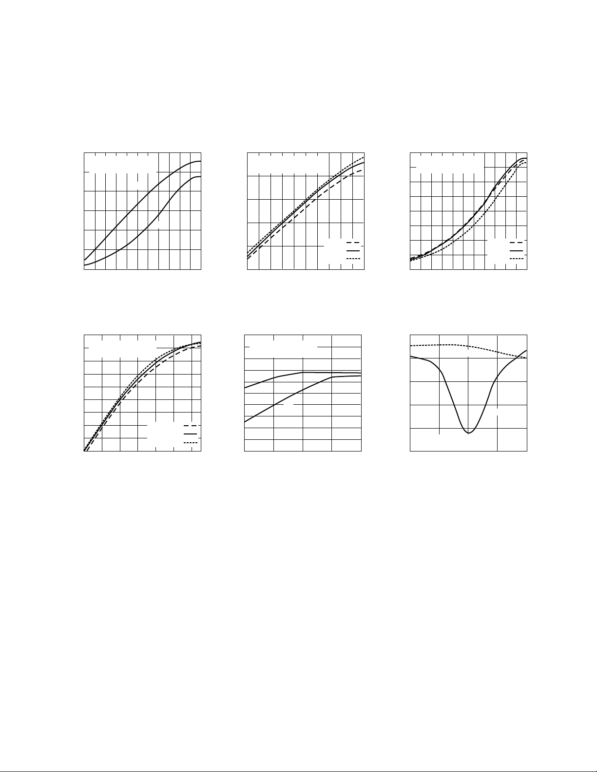
AT-36408 Typical Performance, T
Frequency = 900 MHz, VCE = 4.8 V, I
= 50 mA, pulsed operation, pulse width␣ =␣ 577␣ µsec, duty cycle␣ =␣ 12.5%,
CQ
= 25° C
C
Test Circuit A (GSM), unless otherwise specified.
38
Γ
= 0.88 ∠ -171
source
Γ
= 0.85 ∠ +172
load
34
P
30
26
22
OUTPUT POWER (dBm)
18
14
618161081412 2220 282624
out
η
c
INPUT POWER (dBm)
Figure 1. Output Power and Collector
Efficiency vs. Input Power.
95
80
65
50
35
20
5
38
Γ
source
Γ
(%)
COLLECTOR EFFICIENCY
load
33
28
23
OUTPUT POWER (dBm)
18
13
612810 14 2016 18 22 2624
Figure 2. Output Power vs. Input
Power Over Bias Voltage.
= 0.88 ∠ -171
= 0.85 ∠ +172
INPUT POWER (dBm)
3.6 V
4.8 V
6.0 V
80
Γ
= 0.88 ∠ -171
source
Γ
= 0.85 ∠ +172
load
3.6 V
4.8 V
6.0 V
618161081412 2220 282624
INPUT POWER (dBm)
COLLECTOR EFFICIENCY (%)
70
60
50
40
30
20
10
0
Figure 3. Collector Efficiency vs.
Input Power Over Bias Voltage.
36
Γ
= 0.88 ∠ -171
source
35
Γ
= 0.85 ∠ +172
load
34
33
32
31
30
29
OUTPUT POWER (dBm)
28
27
15 2117 19 23 282725
INPUT POWER (dBm)
TC = +85°C
= +25°C
T
C
= –40°C
T
C
Figure 4. Output Power vs. Input
Power Over Temperature.
36.0
35.8
35.6
35.4
35.2
35.0
34.8
34.6
OUTPUT POWER (dBm)
34.4
34.2
34.0
880
Γ
= 0.88 ∠ -171
source
Γ
= 0.85 ∠ +172
load
FREQUENCY (MHz)
Pin = +26 dBm
η
c
75
71
P
out
67
63
59
55
Figure 5. Output Power and
Collector Efficiency vs. Frequency.
Note: Tuned at 900 MHz, then swept over frequency.
0
Γ
= 0.88 ∠ -171
source
Γ
= 0.85 ∠ +172
load
FREQUENCY (MHz)
Output R.L.
Input R.L.
(%)
-5
-10
-15
RETURN LOSS (dB)
-20
COLLECTOR EFFICIENCY
-25
800 850 950 1000900890 910 920900
Figure 6. Input and Output Return
Loss vs. Frequency.
4-83
 Loading...