

Low Current, High Performance
NPN Silicon Bipolar Transistor
Technical Data
AT-32063
Features
• High Performance Bipolar
Transistor Optimized for
Low Current, Low Voltage
Operation
• 900 MHz Performance:
1.1␣ dB NF, 14.5␣ dB G
A
• Characterized for End-ofLife Battery Use (2.7 V)
• SOT-363 (SC-70) Plastic
Package
• Tape-and-Reel Packaging
Option Available
[1]
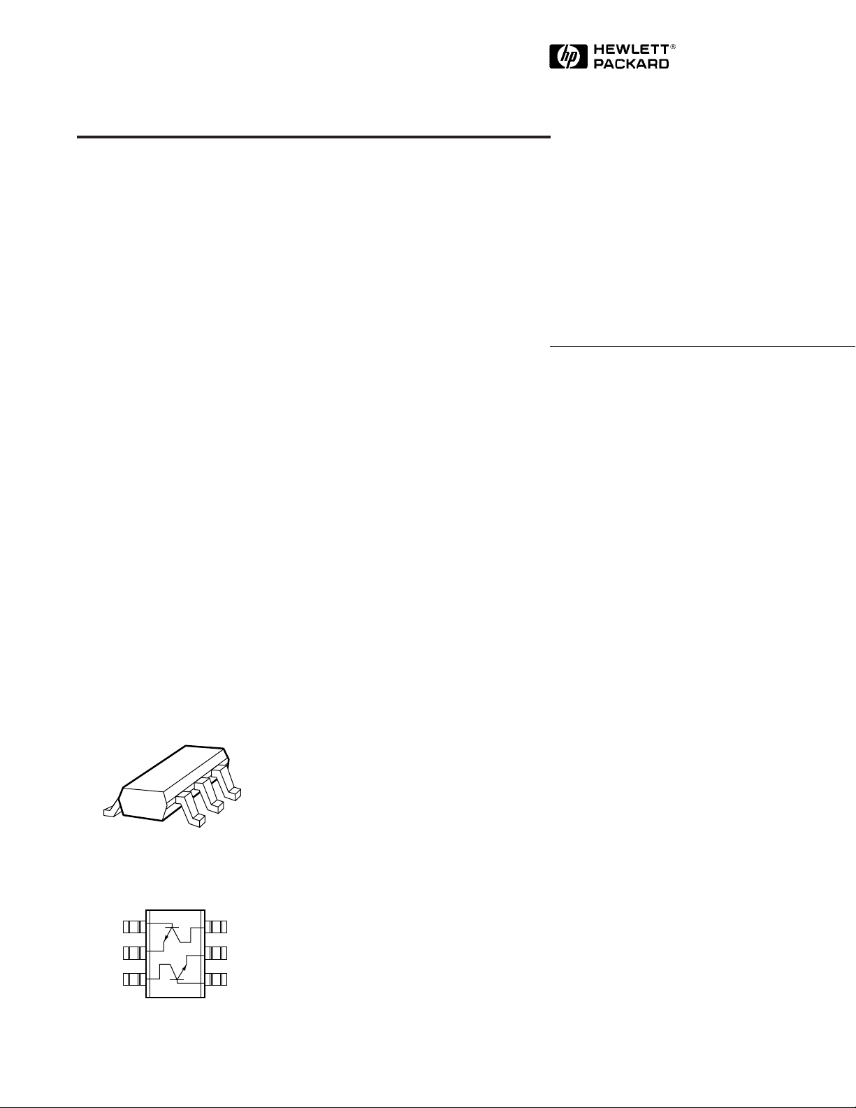
Surface Mount Package SOT-363 (SC-70)
I I
Pin Connections and Package Marking
Description
The AT-32063 contains two high
performance NPN bipolar transistors in a single SOT-363 package.
The devices are unconnected,
allowing flexibility in design. The
pin-out is convenient for cascode
amplifier designs. The SOT-363
package is an industry standard
plastic surface mount package.
The 3.2 micron emitter-to-emitter
pitch and reduced parasitic design
of the transistor yields extremely
high performance products that
can perform a multiplicity of
tasks. The 20 emitter finger
interdigitated geometry yields a
transistor that is easy to match to
and extremely fast, with moderate
power, low noise resistance, and
low operating currents.
Optimized performance at 2.7 V
makes this device ideal for use in
900 MHz, 1.8 GHz, and 2.4 GHz
battery operated systems as an
LNA, gain stage, buffer, oscillator,
or active mixer. Typical amplifier
designs at 900 MHz yield 1.3 dB
noise figures with 12 dB or more
associated gain at a 2.7 V, 5 mA
bias, with noise performance
being relatively insensitive to
input match. High gain capability
at 1 V, 1 mA makes this device a
good fit for 900 MHz pager applications. Voltage breakdowns are
high enough for use at 5 volts.
The AT-3 series bipolar transistors
are fabricated using an optimized
version of Hewlett-Packard’s
10␣ GHz ft , 30 GHz f
max
SelfAligned-Transistor (SAT) process.
The die are nitride passivated for
surface protection. Excellent
device uniformity, performance
and reliability are produced by the
use of ion-implantation, selfalignment techniques, and gold
metallization in the fabrication of
these devices.
1
B
1
2
E
1
3
C
2
6
C
1
5
E
2
4
B
2
4-63
5965-8921E
AT-32063 Absolute Maximum Ratings
[1]
Absolute
Symbol Parameter Units Maximum
Thermal Resistance
θjc = 370°C/W
[2]
:
V
EBO
V
CBO
V
CEO
I
C
P
T
T
j
T
STG
Electrical Specifications, T
Emitter-Base Voltage V 1.5
Collector-Base Voltage V 11
Collector-Emitter Voltage V 5.5
Collector Current mA 40
Power Dissipation
[2,3]
m W 150
Junction Temperature °C 150
Storage Temperature °C -65 to 150
= 25° C
A
Notes:
1. Permanent damage may occur if
any of these limits are exceeded.
2. T
Mounting Surface
Derate at 2.7 mW/°C for TC > 94.5°C.
3.
= 25°C.
4. 150 mW per device.
Symbol Parameters and Test Conditions Units Min. Typ. Max.
14.5
[2]
1.4
[2]
NF Noise Figure; VCE = 2.7 V, IC = 5 mA f = 0.9 GHz dB 1.1
G
h
I
I
FE
CBO
EBO
Associated Gain; VCE = 2.7 V, IC = 5 mA f = 0.9 GHz dB 12.5
A
Forward Current Transfer Ratio; VCE = 2.7 V, IC = 5 mA — 50 270
Collector Cutoff Current; V
Noise Figure; V
= 1 V µA 1.5
EB
= 3 V µA 0.2
CB
Notes:
1. All data is per individual transistor.
2. Test circuit, Figure 1. Numbers reflect device performance de-embedded from circuit losses. Input loss = 0.2 dB;
output␣ loss = 0.3␣ dB.
[2]
[2]
50 Ω
W = 10
L = 450
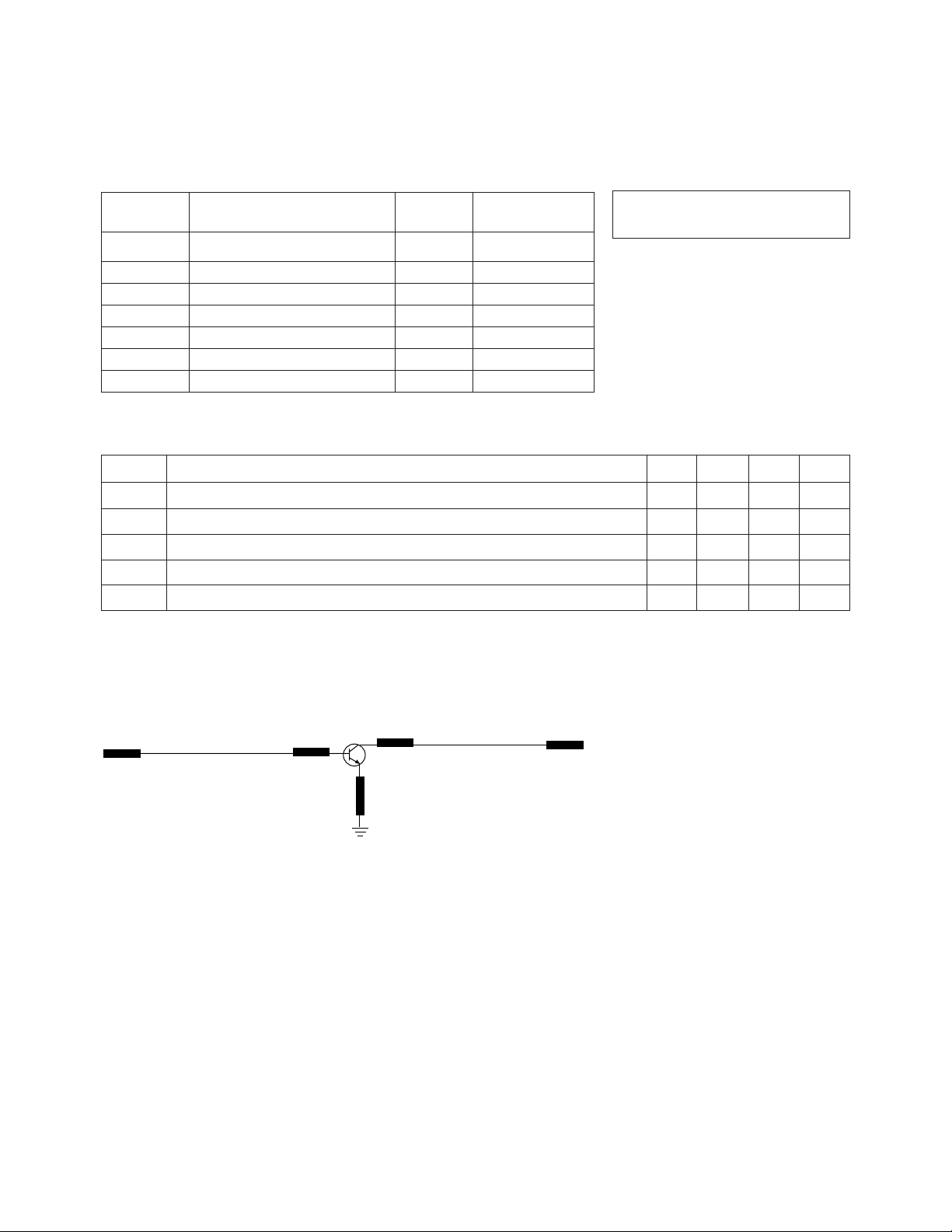
TEST CIRCUIT
BOARD MATERIAL = 0.047 GETEK (ε = 4.3)
DIMENSIONS IN MILS
NOT TO SCALE
W = 20
L = 60
W = 10
L = 100
50 Ω
Figure 1. Test circuit for Noise Figure and Associated Gain.
This circuit is a compromise match between best noise figure, best gain,
stability, and a practical synthesizable match.
4-64
AT-32063 Characterization Information, T
= 25° C
A
Symbol Parameters and Test Conditions Units Typ.
P
G
IP
1 dB
Power at 1 dB Gain Compression (opt tuning); VCE = 2.7 V, IC = 20 mA f = 0.9 GHz dBm 12
Gain at 1 dB Gain Compression (opt tuning); VCE = 2.7 V, IC = 20 mA f = 0.9 GHz dB 16
1 dB
Output Third Order Intercept Point (opt tuning); VCE = 2.7 V, IC = 20 mA f = 0.9 GHz dBm 24
3
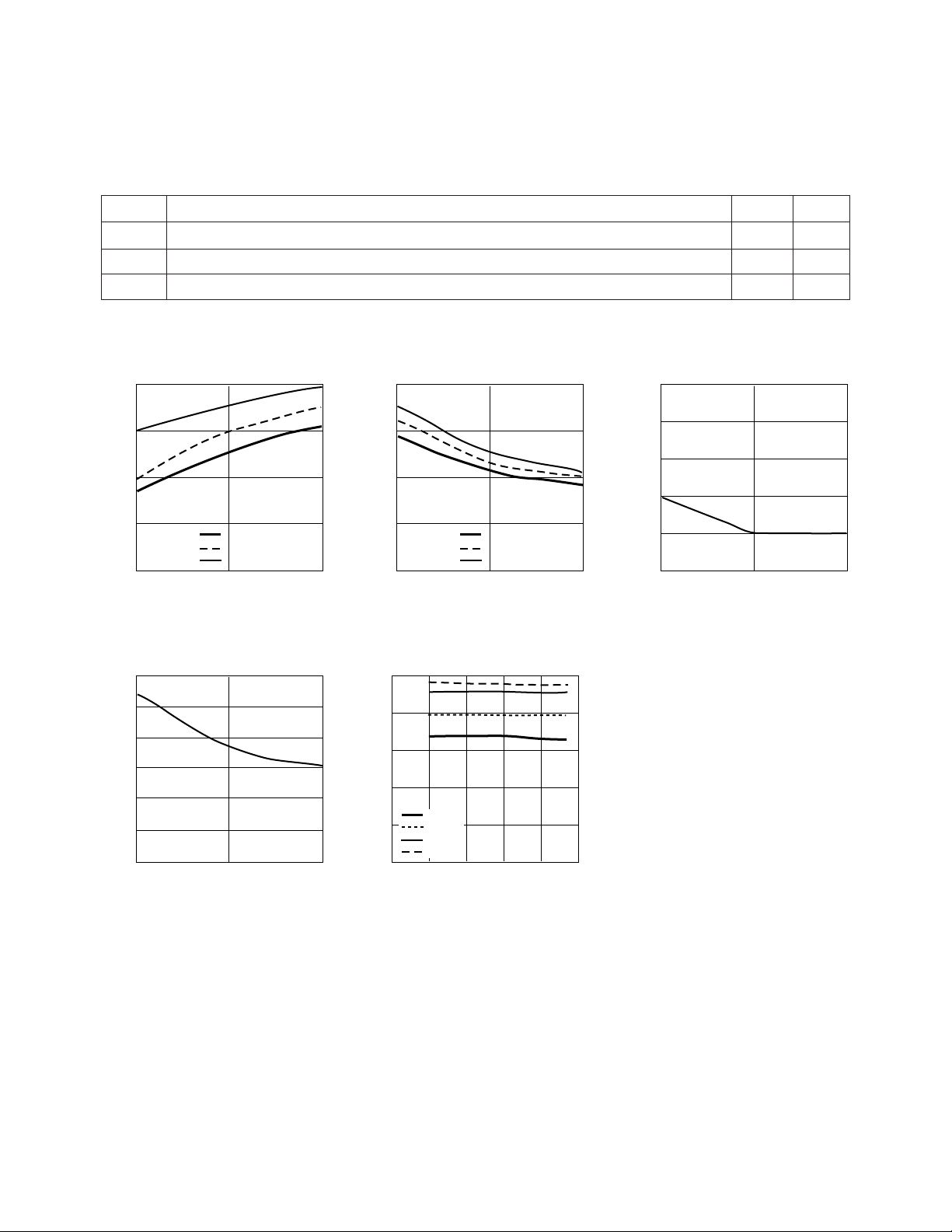
Typical Performance, T
2.00
1.50
(dB)
1.00
NOISE FIGURE
0.50
2.7V/2 mA
2.7V/5 mA
2.7V/20 mA
0
0.9 1.8 2.4
FREQUENCY (GHz)
Figure 2. Minimum Noise Figure vs.
Frequency and Current at VCE = 2.7 V.
18
15
12
(dBm)
9
G1 dB
6
3
0
0.9 1.8 2.4
FREQUENCY (GHz)
Figure 5. 1 dB Compressed Gain vs.
Frequency at VCE = 2.7 V and
IC=20mA.
= 25° C
A
20.0
15.0
(dB)
10.0
Ga
5.0
2.7V/2 mA
2.7V/5 mA
2.7V/20 mA
0
0.9 1.8 2.4
FREQUENCY (GHz)
Figure 3. Associated Gain at
Optimum Noise Match vs. Frequency
and Current at VCE = 2.7 V.
25
20
15
(dBm)
3
IP
10
2 mA
5
5 mA
10 mA
20 mA
0
0 0.5 1.0 1.5 2.0 2.5
FREQUENCY (GHz)
Figure 6. Third Order Intercept vs.
Frequency and Bias at VCE = 2.7 V, with
Optimal Tuning.
15
14
13
(dBm)
12
P1 dB
11
10
0.9 1.8 2.4
FREQUENCY (GHz)
Figure 4. Power at 1 dB Gain
Compression vs. Frequency at
VCE=2.7V and IC = 20 mA.
4-65

AT-32063 Typical Scattering Parameters, Common Emitter, Z
Freq. S
11
S
21
= 50 Ω, V
O
S
12
= 1 V, IC = 1 mA
CE
GHz Mag Ang dB Mag Ang dB Mag Ang Mag Ang
0.1 0.98 -11 11.36 3.7 171 -34.77 0.02 83 0.99 -4
0.5 0.86 -50 10.14 3.21 138 -22.02 0.08 59 0.91 -20
0.9 0.72 -82 8.39 2.63 113 -18.97 0.11 43 0.82 -31
1.0 0.69 -88 7.87 2.48 108 -18.61 0.12 41 0.8 -32
1.5 0.58 -119 5.87 1.97 85 -17.8 0.13 31 0.73 -41
1.8 0.52 -134 4.83 1.74 74 -17.72 0.13 28 0.7 -45
2.0 0.49 -145 4.3 1.64 67 -17.69 0.13 28 0.68 -48
2.4 0.45 -165 3.16 1.44 55 -17.68 0.13 30 0.67 -54
3.0 0.41 166 1.84 1.24 39 -16.99 0.14 37 0.64 -63
4.0 0.42 124 0.17 1.02 16 -13.67 0.21 45 0.6 -81
5.0 0.47 93 -1.15 0.88 -2 -9.84 0.32 38 0.54 -107
25
S
22
AT-32063 Typical Noise Parameters
Common Emitter, Z
Freq. F
GHz dB dB Mag. Ang. —
0.9 0.71 10.4 0.76 50 0.44
1.8 1.37 8.3 0.60 112 0.24
2.4 1.80 7.2 0.50 155 0.10
o
min
= 50 Ω, V
G
= 1 V, IC = 1 mA
CE
A
G
opt
R
n
AT-32063 Typical Scattering Parameters, Common Emitter, Z
Freq. S
11
S
21
20
MSG
15
(dB)
10
GAIN
5
0
-5
0.1 1.1 2.1 3.1 4.1 5.1
Figure 7. Gain vs. Frequency at
V
CE
= 50 Ω, V
O
S
12
S21
FREQUENCY (GHz)
=1V, IC = 1mA.
= 2.7 V, IC = 2 mA
CE
MAG
GHz Mag Ang dB Mag Ang dB Mag Ang Mag Ang
0.1 0.96 -12 16.46 6.66 169 -37.32 0.014 82 0.98 -5
0.5 0.77 -55 14.73 5.45 132 -25.13 0.055 59 0.87 -21
0.9 0.59 -87 12.37 4.15 107 -22.42 0.076 48 0.76 -29
1.0 0.55 -93 11.74 3.86 103 -22.07 0.079 47 0.74 -30
1.5 0.42 -121 9.26 2.90 83 -20.79 0.091 44 0.69 -36
1.8 0.37 -135 8.01 2.52 73 -20.13 0.099 45 0.67 -39
2.0 0.34 -145 7.35 2.33 67 -19.67 0.104 46 0.66 -41
2.4 0.29 -164 6.05 2.01 56 -18.68 0.116 48 0.65 -46
3.0 0.26 167 4.54 1.69 41 -16.95 0.142 50 0.64 -53
4.0 0.28 124 2.73 1.37 20 -13.75 0.205 48 0.61 -68
5.0 0.33 94 1.36 1.17 1 -10.70 0.292 41 0.57 -89
30
MSG
S
22
AT-32063 Typical Noise Parameters
Common Emitter, Z
Freq. F
GHz dB dB Mag. Ang. —
0.9 0.78 14.3 0.65 50 0.31
1.8 1.25 10.7 0.45 105 0.20
2.4 1.57 9.1 0.35 145 0.13
o
min
= 50 Ω, V
G
= 2.7 V, IC = 2 mA
CE
A
G
opt
4-66
25
20
(dB)
R
n
15
GAIN
10
Figure 8. Gain vs. Frequency at
V
CE
MSG
MAG
5
0
0.1 1.1 2.1 3.1 4.1 5.1
=2.7 V, IC = 2mA.
S21
FREQUENCY (GHz)
MSG

AT-32063 Typical Scattering Parameters, Common Emitter, Z
Freq. S
11
S
21
= 50 Ω, V
O
S
12
= 2.7 V, IC = 5 mA
CE
GHz Mag Ang dB Mag Ang dB Mag Ang Mag Ang
0.1 0.87 -19 23.36 14.72 162 -37.77 0.013 80 0.96 -9
0.5 0.52 -72 19.21 9.13 116 -27.03 0.045 60 0.72 -25
0.9 0.34 -101 15.40 5.89 94 -24.01 0.063 58 0.62 -28
1.0 0.31 -106 14.60 5.37 90 -23.41 0.067 58 0.61 -29
1.5 0.22 -129 11.54 3.77 74 -20.85 0.091 58 0.58 -33
1.8 0.19 -141 10.12 3.21 66 -19.52 0.106 58 0.57 -36
2.0 0.17 -150 9.33 2.93 61 -18.72 0.116 57 0.57 -38
2.4 0.14 -169 7.95 2.50 52 -17.22 0.138 56 0.57 -42
3.0 0.12 160 6.34 2.08 39 -15.25 0.173 52 0.56 -49
4.0 0.16 117 4.46 1.67 20 -12.40 0.240 44 0.53 -63
5.0 0.22 93 3.15 1.44 2 -10.03 0.315 33 0.48 -82
35
30
AT-32063 Typical Noise Parameters
Common Emitter, Z
Freq. F
GHz dB dB Mag. Ang. —
0.9 0.98 16.4 0.45 51 0.23
1.8 1.50 11.6 0.29 100 0.16
2.4 1.77 10.1 0.33 153 0.11
o
min
= 50 Ω, V
= 2.7 V, IC = 5 mA
CE
G
A
G
opt
R
n
25
MSG
20
(dB)
15
GAIN
10
5
0
0.1 1.1 2.1 3.1 4.1 5.1
Figure 9. Gain vs. Frequency at
VCE=2.7 V, IC = 5mA.
MAG
S21
FREQUENCY (GHz)
S
22
MSG
AT-32063 Typical Scattering Parameters, Common Emitter, Z
Freq. S
11
S
21
= 50 Ω, V
O
S
12
= 2.7 V, IC = 20 mA
CE
GHz Mag Ang dB Mag Ang dB Mag Ang Mag Ang
0.1 0.55 -41 30.48 33.40 143 -39.81 0.010 74 0.83 -15
0.5 0.20 -107 21.24 11.53 97 -29.18 0.035 72 0.56 -20
0.9 0.13 -137 16.48 6.66 82 -24.63 0.059 72 0.53 -22
1.0 0.13 -141 15.60 6.02 79 -23.79 0.065 71 0.53 -22
1.5 0.10 -164 12.26 4.10 67 -20.43 0.095 68 0.52 -27
1.8 0.09 -178 10.78 3.46 60 -18.88 0.114 66 0.53 -31
2.0 0.09 172 9.93 3.14 56 -17.98 0.126 64 0.53 -34
2.4 0.08 152 8.52 2.67 48 -16.39 0.151 60 0.53 -39
3.0 0.10 127 6.85 2.20 36 -14.4 0.191 54 0.52 -47
4.0 0.15 101 4.92 1.76 18 -11.68 0.261 43 0.48 -61
5.0 0.21 86 3.59 1.51 0 -9.52 0.334 31 0.44 -79
40
35
30
AT-32063 Typical Noise Parameters
Common Emitter, Z
Freq. F
GHz dB dB Mag. Ang. —
0.9 1.51 17.9 0.13 88 0.20
1.8 1.78 12.7 0.20 178 0.13
2.4 1.96 10.6 0.28 235 0.08
o
min
= 50 Ω, V
G
= 2.7 V, IC = 20 mA
CE
A
G
opt
4-67
R
n
MSG
25
(dB)
20
GAIN
15
10
5
0
0.1 1.1 2.1 3.1 4.1 5.1
Figure 10. Gain vs. Frequency at
=2.7 V, IC = 20mA.
V
CE
MAG
S21
FREQUENCY (GHz)
S
22
MSG

AT-32063 Typical Scattering Parameters, Common Emitter, Z
0
5
S21
10
15
20
30
25
0.1 1.1 2.1 3.1 4.1 5.1
GAIN
(dB)
FREQUENCY (GHz)
Figure 11. Gain vs. Frequency at
VCE=5 V, IC = 2mA.
MSG
MSG
MAG
0
5
S21
10
15
20
40
25
30
35
0.1 1.1 2.1 3.1 4.1 5.1
GAIN
(dB)
FREQUENCY (GHz)
Figure 12. Gain vs. Frequency at
V
CE
=5 V, IC = 20mA.
MSG
MSG
MAG
Freq. S
11
S
21
= 50 Ω, V
O
S
12
= 5 V, IC = 2 mA
CE
GHz Mag Ang dB Mag Ang dB Mag Ang Mag Ang
0.1 0.96 -12 16.50 6.69 169 -38.44 0.012 82 0.98 -5
0.5 0.78 -53 14.84 5.52 133 -26.20 0.049 60 0.88 -19
0.9 0.59 -84 12.5 4.23 108 -23.4 0.068 50 0.79 -27
1.0 0.56 -90 11.92 3.94 104 -23.04 0.070 49 0.77 -28
1.5 0.42 -117 9.46 2.97 84 -21.71 0.082 46 0.72 -33
1.8 0.36 -131 8.21 2.57 74 -21.04 0.089 47 0.70 -36
2.0 0.33 -140 7.55 2.38 68 -20.56 0.094 48 0.69 -39
2.4 0.28 -159 6.24 2.05 57 -19.54 0.105 50 0.69 -43
3.0 0.24 171 4.72 1.72 43 -17.76 0.129 53 0.68 -50
4.0 0.25 126 2.88 1.39 21 -14.47 0.189 52 0.66 -64
5.0 0.31 95 1.49 1.19 3 -11.32 0.272 45 0.63 -83
AT-32063 Typical Noise Parameters
Common Emitter, Z
Freq. F
GHz dB dB Mag. Ang. —
0.9 0.75 13.7 0.74 47 0.37
1.8 1.26 10.8 0.55 101 0.22
2.4 1.60 9.6 0.45 139 0.13
o
min
= 50 Ω, V
G
= 5 V, IC = 2 mA
CE
A
G
opt
R
n
S
22
AT-32063 Typical Scattering Parameters, Common Emitter, Z
Freq. S
GHz Mag Ang dB Mag Ang dB Mag Ang Mag Ang
0.1 0.61 -36 30.56 33.74 145 -40.46 0.01 75 0.86 -14
0.5 0.22 -91 21.75 12.23 98 -29.90 0.03 72 0.6 -19
0.9 0.13 -115 17.02 7.10 83 -25.40 0.05 72 0.57 -21
1.0 0.12 -118 16.14 6.41 81 -24.56 0.06 71 0.57 -21
1.5 0.08 -137 12.80 4.36 68 -21.23 0.09 69 0.57 -26
1.8 0.06 -148 11.31 3.68 62 -19.69 0.10 66 0.57 -30
2.0 0.06 -159 10.46 3.33 58 -18.79 0.12 65 0.57 -32
2.4 0.04 175 9.02 2.83 50 -17.21 0.14 61 0.57 -37
3.0 0.05 131 7.35 2.33 39 -15.22 0.17 56 0.56 -45
4.0 0.10 99 5.39 1.86 21 -12.48 0.24 46 0.54 -58
5.0 0.16 86 4.05 1.6 3 -10.27 0.31 34 0.50 -75
AT-32063 Typical Noise Parameters
Common Emitter, Z
Freq. F
GHz dB dB Mag. Ang. —
0.9 1.50 18.6 0.18 74 0.20
1.8 1.78 13.3 0.19 147 0.16
2.4 1.96 11.3 0.24 198 0.14
o
min
11
= 50 Ω, V
G
= 5 V, IC = 20 mA
CE
A
G
opt
= 50 Ω, V
O
S
21
R
n
S
12
= 5 V, IC = 20 mA
CE
S
22
4-68

Package Dimensions
Outline 63 (SOT-363/SC-70)
1.30 (0.051)
REF.
2.20 (0.087)
2.00 (0.079)
2.20 (0.087)
1.80 (0.071)
0.10 (0.004)
0.00 (0.00)
0.25 (0.010)
0.15 (0.006)
DIMENSIONS ARE IN MILLIMETERS (INCHES)
1.35 (0.053)
1.15 (0.045)
0.650 BSC (0.025)
1.00 (0.039)
0.80 (0.031)
0.30 REF.
10°
Part Number Ordering Information
Part Number No. of Devices Container
AT-32063-TR1 3000 7" Reel
AT-32063-BLK 100 antistatic bag
0.30 (0.012)
0.10 (0.004)
0.425 (0.017)
TYP.
0.20 (0.008)
0.10 (0.004)
4-69

Device Orientation
REEL
USER
FEED
DIRECTION
COVER TAPE
Tape Dimensions
For Outline 63
P
P
0
CARRIER
TAPE
TOP VIEW
END VIEW
4 mm
8 mm
D
II II II II
P
2
E
F
W
CAVITY
PERFORATION
CARRIER TAPE
DISTANCE
D
t
(CARRIER TAPE THICKNESS)
1
8° MAX.
A
0
K
0
1
B
0
DESCRIPTION SYMBOL SIZE (mm) SIZE (INCHES)
LENGTH
WIDTH
DEPTH
PITCH
BOTTOM HOLE DIAMETER
DIAMETER
PITCH
POSITION
WIDTH
THICKNESS
CAVITY TO PERFORATION
A
B
K
P
D
D
P
E
W
t
F
0
0
0
1
0
1
2.24 ± 0.10
2.34 ± 0.10
1.22 ± 0.10
4.00 ± 0.10
1.00 + 0.25
1.55 ± 0.05
4.00 ± 0.10
1.75 ± 0.10
8.00 ± 0.30
0.255 ± 0.013
3.50 ± 0.05
0.088 ± 0.004
0.092 ± 0.004
0.048 ± 0.004
0.157 ± 0.004
0.039 + 0.010
0.061 ± 0.002
0.157 ± 0.004
0.069 ± 0.004
0.315 ± 0.012
0.010 ± 0.0005
0.138 ± 0.002
(WIDTH DIRECTION)
CAVITY TO PERFORATION
(LENGTH DIRECTION)
2
2.00 ± 0.05
P
0.079 ± 0.002
5° MAX.
4-70
 Loading...