

查询HMC271LP4供应商
HMC271LP4 / 271LP4E
v02.0705
1 dB LSB GaAs MMIC 5-BIT SERIAL
CONTROL DIGITAL ATTENUATOR, 0.7 - 3.7 GHz
9
ATTENUATORS - SMT
Typical Appli cations
The HMC271LP4 / HMC271LP4E is ideal for:
• Cellular/3G Infrastructure
• Fixed Wireless & WiMax
• Test Instrumentation
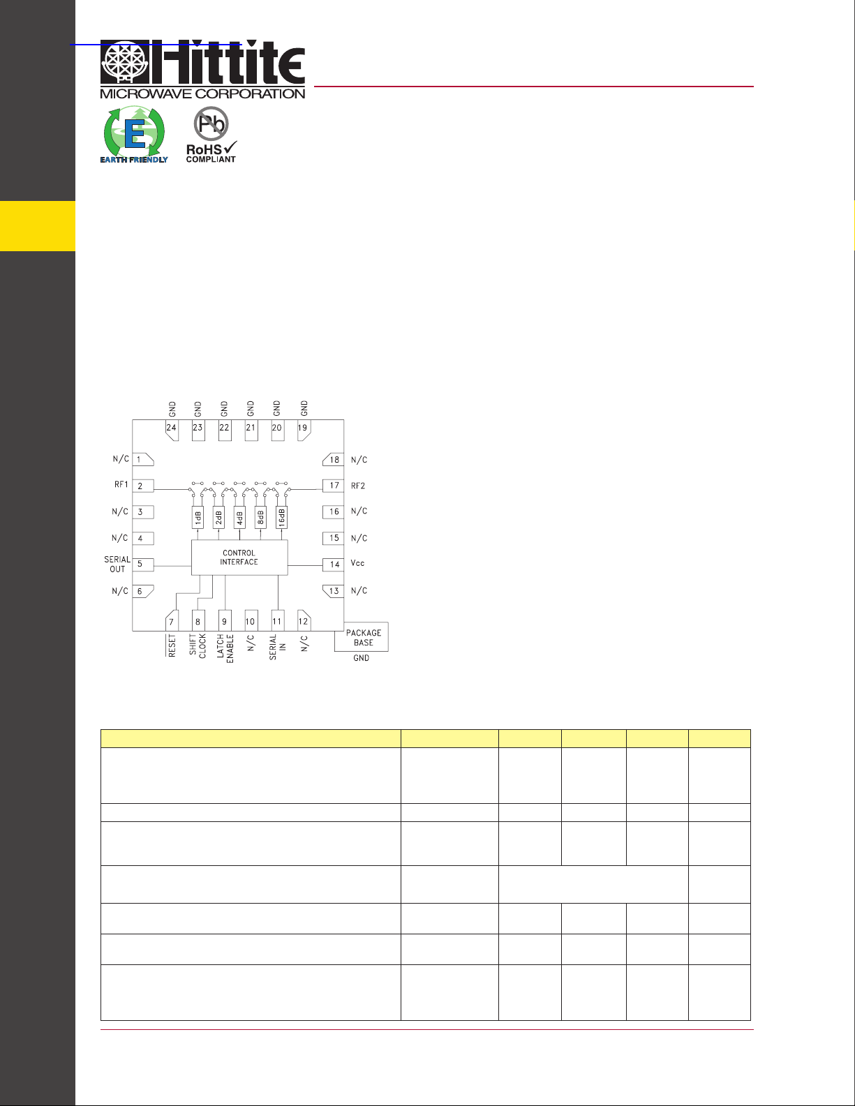
Functional Diagram
Features
1 dB LSB Steps to 31 dB
CMOS Compatible Serial Data Interface
SPI Compatible Serial Output
+/- 0.4 dB Typical Bit Error
4 x 4 mm
QFN Plastic Package
General Description
The HMC271LP4 & HMC271LP4E are broadband 5bit positive control GaAs IC digital attenuators with
serial-to-parallel drivers in low cost leadless QFN
4x4 mm SMT packages. Covering 0.7 to 3.7 GHz,
the insertion loss is typically less than 2.5 dB. The
attenuator bit values are 1 (LSB), 2, 4, 8, and 16 dB
for a total attenuation of 31 dB. Accuracy is excellent
at ± 0.4 dB typical with an IIP3 of up to +48 dBm. Five
bit CMOS compatible serial control words are used to
select each attenuation state. A single Vcc bias of +3V
to +5V applied through an external 5k Ohm resistor is
required.
9 - 14
Electrical Specifications, T
Parameter Frequency Min. Typical Max. Units
Insertion Loss
Attenuation Range 0.7 - 3.7 GHz 31 dB
Return Loss (RF1 & RF2, All Atten. States)
Attenuation Accuracy: (Referenced to Inser tion Loss)
All Attenuation States 0.7 - 3.7 GHz ± 0.4 ± 5% of Atten. Setting Max dB
Input Power for 0.1 dB Compression
Input Third Order Intercept Point
(Two-tone Input Power = 0 dBm Each Tone)
Switching Characteristics
tRISE, tFALL (10/90% RF)
tON, tOFF (Latch Enable to 10/90% RF)
= +25° C, Vcc = +3V to +5V
A
0.7 - 1.4 GHz
1.4 - 2.3 GHz
2.3 - 2.7 GHz
2.7 - 3.7 GHz
0.7 - 1.4 GHz
1.4 - 2.7 GHz
2.7 - 3.7 GHz
Vcc = 5V
Vcc = 3V
Vcc = 5V
Vcc = 3V
0.7 - 3.7 GHz
0.7 - 3.7 GHz
0.7 - 3.7 GHz
1.9
2.3
2.6
2.8
12
15
16
24
22
48
46
750
830
2.4
2.8
3.1
3.3
For price, delivery, and to place orders, please contact Hittite Microwave Corporation:
20 Alpha Road, Chelmsford, MA 01824 Phone: 978-250-3343 Fax: 978-250 -3373
Order On-line at www.hittite.com
dB
dB
dB
dB
dB
dB
dB
dBm
dBm
dBm
dBm
ns
ns
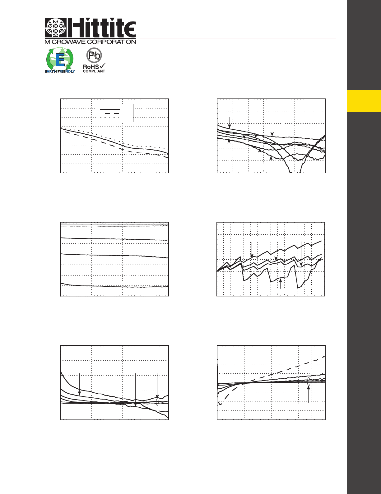
Insertion Loss
0
-0.5
-1
-1.5
-2
-2.5
INSERTION LOSS (dB)
-3
-3.5
-4
0.5 1 1.5 2 2.5 3 3.5 4
FREQUENCY (GHz)
+25C
+85C
-40C
HMC271LP4 / 271LP4E
v02.0705
CONTROL DIGITAL ATTENUATOR, 0.7 - 3.7 GHz
1 dB LSB GaAs MMIC 5-BIT SERIAL
Return Loss RF1, RF2
(Only Major States are Shown)
0
-5
16 dB 31 dB
-10
-15
-20
RETURN LOSS (dB)
2 dB
-25
-30
0.5 1 1.5 2 2.5 3 3.5 4
8 dB4 dB
1 dB
I.L.
FREQUENCY (GHz)
9
Normalized Attenuation
(Only Major States are Shown)
0
-5
-10
-15
-20
-25
-30
NORMALIZED ATTENUATION (dB)
-35
0.5 1 1.5 2 2.5 3 3.5 4
FREQUENCY (GHz)
Bit Error vs. Frequency
(Only Major States are Shown)
4
3
2
1
BIT ERROR (dB)
0
-1
16 dB
31 dB
0.5 1 1.5 2 2.5 3 3.5 4
FREQUENCY (GHz)
Bit Error
vs. Attenuation State
2
1.5
1
0.5
0
BIT ERROR (dB)
-0.5
-1
02468101214161820222426283032
0.9 GHz
ATTENUATION STATE (dB)
1.9 GHz
3.5 GHz
2.4 GHz
ATTENUATORS - SMT
Relative Phase vs. Frequency
(Only Major States are Shown)
100
75
50
1, 2, 4 dB8 dB
25
0
-25
-50
RELATIVE PHASE (deg.)
-75
-100
0 0.5 1 1.5 2 2.5 3 3.5 4
FREQUENCY (GHz)
31 dB
16 dB
1, 2, 4, 8 dB
Note: All Data Typical Over Voltage (+3V to +5V) & Temperature (-40 to +85 deg. C.).
For price, delivery, and to place orders, please contact Hittite Microwave Corporation:
20 Alpha Road, Chelmsford, MA 01824 Phone: 978-250-3343 Fax: 978-250 -3373
Order On-line at www.hittite.com
9 - 15
9
v02.0705
CONTROL DIGITAL ATTENUATOR, 0.7 - 3.7 GHz
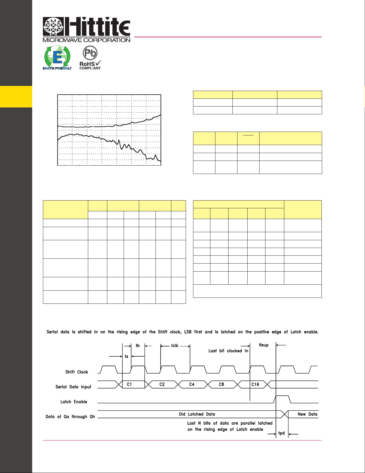
Worst Case Step Error
Between Successive Attenuation States
1.2
1
0.8
0.6
0.4
0.2
0
-0.2
-0.4
STEP ERROR (dB)
-0.6
-0.8
-1
-1.2
0.5 1 1.5 2 2.5 3 3.5 4
FREQUENCY (GHz)
HMC271LP4 / 271LP4E
1 dB LSB GaAs MMIC 5-BIT SERIAL
CMOS Control Voltages
State Vcc = +5V Vcc = +3V
Low 0 to 1.3V 0 to 0.7V
High 3.5 to 5.0V 2.3 to 3.0V
Serial Input Truth Table
Latch
Enable
X X L Shift register cleared
X
Ç
Shift
Lock
Ç
Reset Function
HShift register locked
XH
Contents of shift register
transferrred to output latches
ATTENUATORS - SMT
Timing
Parameter
Serial IN Setup Time ts 20 - 100 - ns
Hold time from Serial
In to Shift Clock
Setup time from
Shift clock to Latch
Enable
Propogation delay,
Latch enable to Qa
through Qh
Setup time from
Reset to Shift Clock
Clock Frequency
(1/t cl k)
Symbol Vcc = +5V Vcc = +3V Unit
Min. Max. Min. Max.
th 0 - 5 - ns
tlsup 40 - 100 - ns
tpd - 30 - 70 ns
-20-50-ns
fclk - 30 - 10 MHz
Timing Diagram
Truth Table
Serial Data Input Attenuation
C1 C2 C4 C8 C16
High High High High High
Low High High High High 1 dB
High Low High High High 2 dB
High High Low High High 4 dB
High High High Low High 8 dB
High High High High Low 16 dB
Low Low Low Low Low
Any combination of the above states will provide an attenuation
approximately equal to the sum of the bits selected.
Setting
RF1 - RF2
Reference
I.L.
31 dB
Max. Atten.
9 - 16
For price, delivery, and to place orders, please contact Hittite Microwave Corporation:
20 Alpha Road, Chelmsford, MA 01824 Phone: 978-250-3343 Fax: 978-250 -3373
Order On-line at www.hittite.com

v02.0705
CONTROL DIGITAL ATTENUATOR, 0.7 - 3.7 GHz
Absolute Maximum Ratings
Digital Inputs (Reset, Shift Clock,
Latch Enable & Serial In)
Digital Outputs (Serial Out) -0.5 to (Vcc+0.5)Vdc
DC Current on Serial Output ±35mA
Bias Voltage (Vcc) +7.0 Vdc
Storage Temperature -65 to +150 °C
Operating Temperature -40 to +85 °C
RF Input Power (0.7 - 3.7 GHz) +26 dBm
ESD Sensitivity (HBM) Class 1A
Outline Drawing
-1.5 to (Vcc + 1.5) Vdc
HMC271LP4 / 271LP4E
1 dB LSB GaAs MMIC 5-BIT SERIAL
ELECTROSTATIC SENSITIVE DEVICE
OBSERVE HANDLING PRECAUTIONS
9
NOTES:
1. LEADFRAME MATERIAL: COPPER ALLOY
2. DIMENSIONS ARE IN INCHES [MILLIMETERS]
3. LEAD SPACING TOLERANCE IS NON -CUM ULATIVE
4. PAD BURR LENGTH S HALL BE 0.15mm MA XIMUM.
PAD BURR HEIGH T SHALL BE 0. 05mm MA XIMUM.
5. PACKAGE WARP SH ALL NOT EXCEED 0.05mm.
6. ALL GROUND LEADS AND GROUND PADDLE MUST B E
SOLDERED TO PCB RF GROU ND.
7. REFER TO HITTITE APPL ICATION NOTE FOR SUGGESTED
LAND PATTERN.
Package Information
Part Number Package Body Material Lead Finish MSL Rating Package Marking
HMC271LP4 Low Stress Injection Molded Plastic Sn /Pb Solder
HMC271LP4E RoHS -compliant Low Stress Injection Molded Plastic 100% matte Sn
[1] Max peak re ow temperature of 23 5 °C
[2] Max peak re ow temperature of 260 °C
[3] 4-Digit lot number XXXX
MSL1
MSL1
[1]
[2]
ATTENUATORS - SMT
[3]
H271
XXXX
H271
XXXX
For price, delivery, and to place orders, please contact Hittite Microwave Corporation:
20 Alpha Road, Chelmsford, MA 01824 Phone: 978-250-3343 Fax: 978-250 -3373
Order On-line at www.hittite.com
9 - 17

Pin Descriptions
HMC271LP4 / 271LP4E
v02.0705
1 dB LSB GaAs MMIC 5-BIT SERIAL
CONTROL DIGITAL ATTENUATOR, 0.7 - 3.7 GHz
9
ATTENUATORS - SMT
Pin Number Function Description Interface Schematic
1, 3, 4, 6, 10, 12, 13,
15, 16, 18
2, 17 RF1, RF2
5 Serial Out
7 Reset
8 Shift clock
9 Latch Enable
11 Serial In
N/C
These pins should be connected to PCB RF ground to
maximize performance.
This pin is DC coupled and matched to 50 Ohms
Blocking capacitors are required. Select value based on lowest
frequency of operation.
Serial data output. Serial input data
delayed by 8 clock cycles.
See truth table, control voltage table and timing diagram.
9 - 18
14 Vcc Supply Voltage.
19 - 24 GND
For price, delivery, and to place orders, please contact Hittite Microwave Corporation:
20 Alpha Road, Chelmsford, MA 01824 Phone: 978-250-3343 Fax: 978-250 -3373
Package bottom has an exposed metal paddle that must also
be connected to RF/DC Ground.
Order On-line at www.hittite.com

Application Circuit
HMC271LP4 / 271LP4E
v02.0705
1 dB LSB GaAs MMIC 5-BIT SERIAL
CONTROL DIGITAL ATTENUATOR, 0.7 - 3.7 GHz
9
DC blocking capacitors C1 & C2 are required on RF1 & RF2. Choose C1 = C2 = 100 ~ 300 pF to allow lowest customer speci c
frequency to pass with minimal loss. R1 = 5k Ohm is required to supply voltage to the circuit through either PIN 2 or PIN 17.
ATTENUATORS - SMT
For price, delivery, and to place orders, please contact Hittite Microwave Corporation:
20 Alpha Road, Chelmsford, MA 01824 Phone: 978-250-3343 Fax: 978-250 -3373
Order On-line at www.hittite.com
9 - 19

9
HMC271LP4 / 271LP4E
v02.0705
1 dB LSB GaAs MMIC 5-BIT SERIAL
CONTROL DIGITAL ATTENUATOR, 0.7 - 3.7 GHz
Logic / Functional Diagram
ATTENUATORS - SMT
Programming Example to Select 1 dB State
9 - 20
For price, delivery, and to place orders, please contact Hittite Microwave Corporation:
20 Alpha Road, Chelmsford, MA 01824 Phone: 978-250-3343 Fax: 978-250 -3373
Order On-line at www.hittite.com

Evaluation Circuit Board
HMC271LP4 / 271LP4E
v02.0705
1 dB LSB GaAs MMIC 5-BIT SERIAL
CONTROL DIGITAL ATTENUATOR, 0.7 - 3.7 GHz
9
List of Materials for Evaluation PCB 108782
Item Description
J1 - J2 PCB Mount SMA Connector
J3 2 mm Molex Header
C1, C2 100 pF Capacitor, 0402 Pkg.
C3 0.01 μF Capacitor, 0402 Pkg.
R1 5k Ohm Resistor, 0402 Pkg.
U1
[2]
PCB
[1] Reference this number when ordering complete evaluation PCB
[2] Circuit Board Material: Rogers 4350
HMC271LP4 / HMC271LP4E
Digital Attenuator
108780 Evaluation PCB
The circuit board used in the nal application
should use RF circuit design techniques. Signal
lines should have 50 ohm impedance while the
package ground leads and exposed ground paddle
should be connected directly to the ground plane
similar to that shown below. A suf cient number of
VIA holes should be used to connect the top and
bottom ground planes. The evaluation circuit board
as shown is available from Hittite Microwave Corporation upon request.
ATTENUATORS - SMT
[1]
For price, delivery, and to place orders, please contact Hittite Microwave Corporation:
20 Alpha Road, Chelmsford, MA 01824 Phone: 978-250-3343 Fax: 978-250 -3373
Order On-line at www.hittite.com
9 - 21
 Loading...