HIT HA13568AT Datasheet

HA13568AT
CD-ROM Combo Driver
ADE-207-261A (Z)
2nd Edition
December 1998
Description
The HA13568AT is combination of Spindle, Forcus, Tracking, Slide, Tray designed for CD-ROM and
have following functions and features.
Features
• 1.5 A sensorless spindle driver
• 0.5 A BTL focus driver
• 0.5 A BTL tracking driver
• 1.5 A H bridge slide motor driver
• 0.5 A H bridge tray motor driver
• Over temperature shut down (OTSD)
• Voltage regulator control circuit
Functions
• Sensorless driver with self start
• Soft switching drive
• Snubberless
• Low output saturation voltage
• Direct PWM slide driver

HA13568AT
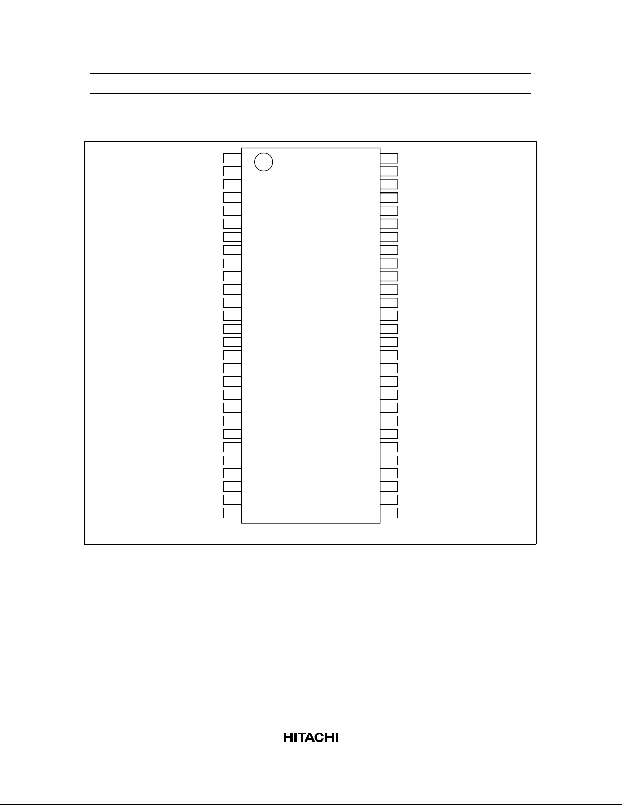
Pin Arrangement
GND
FCSREF
FCSIN
FCSRS
TRRRS
VFCS
FCSP
FCGND
FCSN
TRRP
TRRN
TRYP
TRYN
VSLD
SLGND
SLDN
SLDP
VBST
B1
B2
RNF
W
VSPN
WFIL
VFIL
GND
1
2
3
4
5
6
7
8
9
10
11
12
13
14
15
16
17
18
19
20
21
U
22
V
23
24
25
26
27
28
56
55
54
53
52
51
50
49
48
47
46
45
44
43
42
41
40
39
38
37
36
35
34
33
32
31
30
29
GND
TRRREF
TRRIN
NC
NC
NC
TRYLIM
TRYR
TRYF
SLDIN
SLDLIM
RT
CT2
VSS
CT3
CT1
CE
VREGF
VREGS
BRKSEL
PHASE
PC
CT
AGC
VCTL
REFIN
UFIL
GND
(Top view)
2

HA13568AT
Pin Description
Pin No. Pin Name Function
2 FCSREF FCS driver block reference voltage
3 FCSIN FCS control input pin
4 FCSRS FCS sense pin
5 TRRRS TRR sense pin
6 VFCS FCS driver and TRR driver power supply
7 FCSP FCS driver P output
8 FCGND FCS driver and TRR driver GND
9 FCSN FCS driver N output
10 TRRP TRR driver P output
11 TRRN TRR driver N output
12 TRYP TRY driver P output
13 TRYN TRY driver N output
14 VSLD SLD driver and TRY driver power supply
15 SLGND SLD driver and TRY driver GND
16 SLDN SLD driver N output
17 SLDP SLD driver P output
18 VBST Booster output pin. This circuit generates a voltage about 1.5 V above that of the
VSPN pin.
19 B1 Booster pumping capacitor connection
20 B2
21 RNF Spindle driver current detection
22 U U phase output
23 V V phase output
24 W W phase output
25 VSPN Spindle and booster power supply
26 WFIL W phase low pass filter. Connect a filter C to this pin during GND.
27 VFIL V phase low pass filter. Connect a filter C to this pin during GND.
30 UFIL U phase low pass filter. Connect a filter C to this pin during GND.
31 REFIN Reference voltage of spindle and slide
32 VCTL Spindle control input. Generates forward torque when a DC voltage higher than
REFIN is applied, and brake when a DC voltage lower than REF is applied.
33 AGC For AGC. Holds the level used for IC internal processing fixed even if the B-EMF
level fluctuates due to the rotation speed.
34 CT Spindle center tap
35 PC Spindle driver phase compensation
3

HA13568AT
Pin Description (cont)
Pin No. Pin Name Function
36 PHASE Outputs the B-EMF zero cross phase. Open corrector. (See the timing chart)
37 BRKSEL To select the brake mode. Lo: Short brake, Hi: Reverse full brake
(when forward torque input: BRKSEL = H)
38 VREGS Voltage regulator sense pin (VREGS ≈ 3.3 V output)
39 VREGF Voltage regulator force pin
40 CE Chip enable. Input Hi: active
41 CT1 Time constant for clock oscillator circuit. The clock oscillator frequency is
determined by the external capacitor and resistor Ct1 and Rt.
42 CT3 Time constant for PWM carrier oscillator. The carrier frequency is determined by
the external capacitor and resistor Ct3 and Rt.
43 VSS Control block power supply. 5 V
44 CT2 Time constant for start-up oscillator. The start-up oscillator frequency is
determined by the external capacitor and resistor Ct2 and Rt.
45 RT Reference voltage (3.3 V). The IC’s internal reference current is determined by
this voltage and the external resistor Rt.
46 SLDLIM SLD output maximum duty setting
47 SLDIN SLD control input pin
48 TRYF TRY driver forward input
49 TRYR TRY driver reverese input
50 TRYLIM TRY output voltage setting pin
51 NC No connection
52 NC
53 NC
54 TRRIN TRR control input pin
55 TRRREF TRR driver block reference voltage
1, 28, 29, 56, TAB GND
4

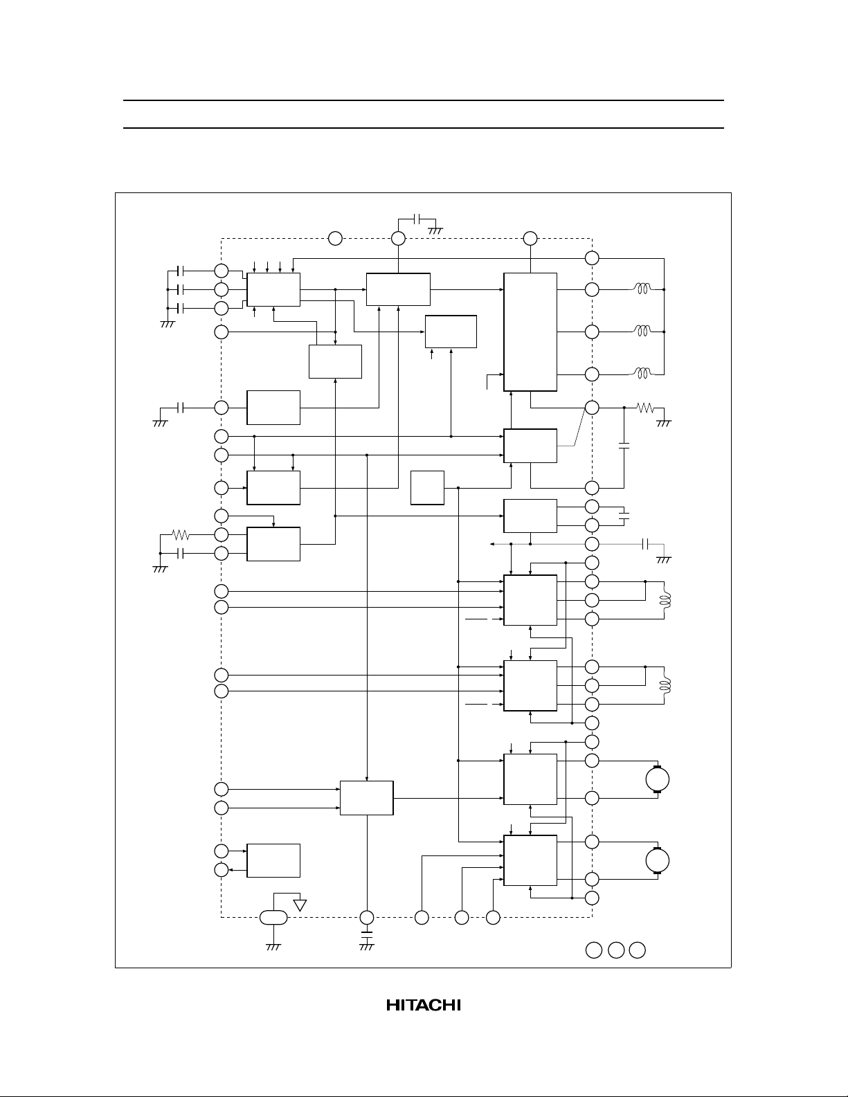
Block Diagram
UFIL
30
VFIL
27
WFIL
26
PHASE
36
CT2
VCTL
REFIN
CE
Rt
RT
CT1
FCSIN
TRRIN
SLDIN
VREGS
VREGF
44
32
31
37
40
45
41
3
2
54
55
47
46
38
39
Ct2
BRKSEL
Ct1
FCSREF
TRRREF
SLDLIM
C102
VSS VSPNAGC
WVU
B-EMF
detection
Vspn
Tmask
Mask
time
Start-up
circuit
Brake
CLK
CLK
OSC
Vreg
TAB 42 48
SLD
control
CT3
Commutation
OTSD
TRYLIM
Ct3
50
Vref
Drive
mode
TRYF
Vbst
Vfcs
2
Vfcs
2
Vbst
49
TRYR
1.5A
SPN
output
Vbst
Vbst
1.5AH
bridge
Vbst
0.5AH
bridge
253343
U
V SPN
W
Current
control
Bias
P
0.5A
BTL
N
P
0.5A
BTL
N
P
N
P
N
CT
34
U
22
V
23
W
24
RNF
21
PC
35
B1
19
B2
20
VBST
18
6
VFCS
FCSP
7
FCSRS
4
FCSN
9
TRRP
10
TRRRS
5
TRRN
11
8
FCGND
14
VSLD
SLDP
17
SLDN
16
TRYP
12
TRYN
13
15
SLGND
51 , ,52 53 : NC pin
HA13568AT
Rnf
FCS
TRR
SLD
M
TRY
M
5

HA13568AT
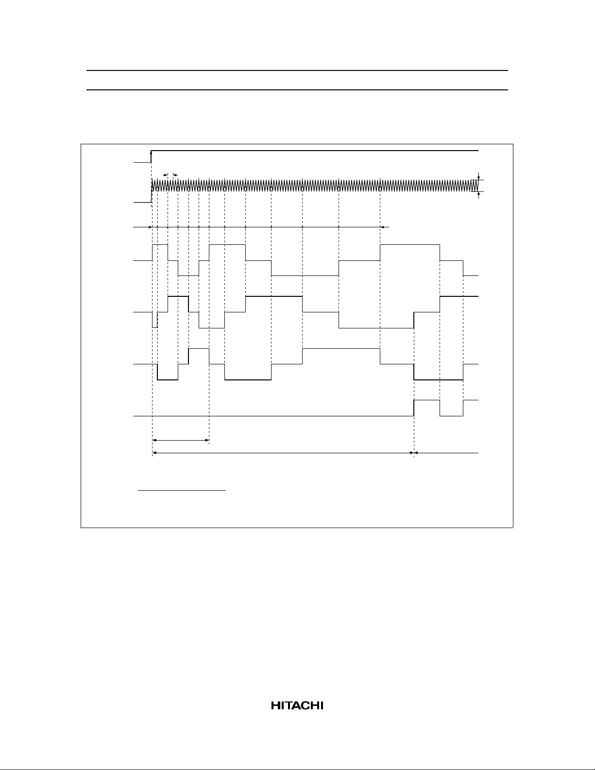
Timing Chart
1. Start-up
CE
CT2
Output
current
(U phase)
Output
current
(V phase)
Output
current
(W phase)
PHASE 0
0
0
+
0
−
+
0
−
+
0
−
Tc2
4Tc2
2Tc2
4Tc2
4Tc2
B-EMF
Mask period
4Tc2
4Tc2
6Tc2
8Tc2
10Tc2
12Tc2
Synchronous mode B-EMF mode
14Tc2
16Tc2
Vhct2
Vlct2
Note: Tc2 is as follows.
8 (Vhct2 − Vlct2) Rt Ct2
Tc2 =
Where, Vhct2
Vlct2
6
Vrt
: CT2 pin high voltage (See electrical characteristics)
: CT2 pin low voltage (See electrical characteristics)

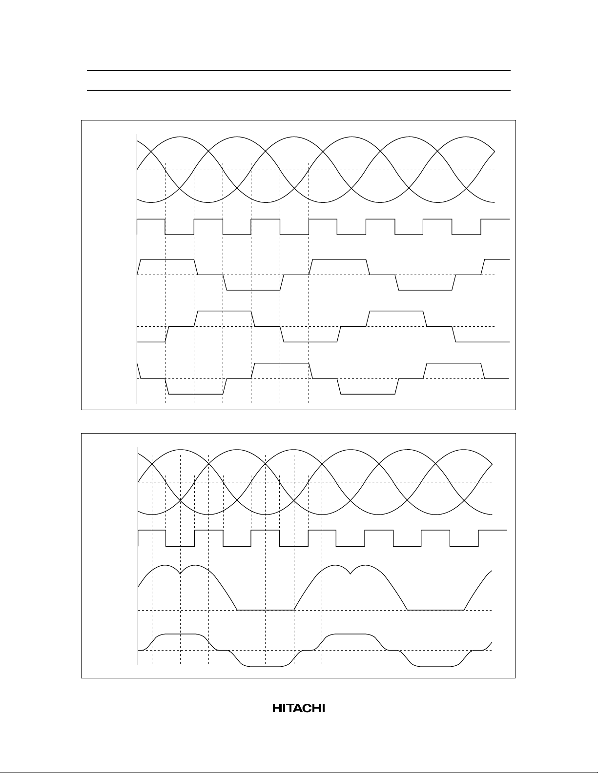
2. Acceleration (switching mode)
UVW
HA13568AT
Reverse
start-up
voltage
B-EMF
PHASE
Output
current
(U phase)
Output
current
(V phase)
Output
current
(W phase)
+
0
−
0
+
0
−
+
0
−
+
0
−
3. Running (soft switching mode)
Reverse
start-up
voltage
B-EMF
PHASE
Output
voltage
(U phase)
Output
current
(U phase)
UVW
+
0
−
0
0
+
0
−
7
 Loading...