HIT HA13566AF Datasheet

HA13566AF
Combo (Spindle & VCM) Driver
ADE-207-250 (Z)
1st Edition
December 1997
Description
The HA13566AF is combination of Spindle and VCM Driver designed for HDD and have following
functions and features.
Functions
• 1.0 A max/3-phase spindle motor driver
• 400 mA max VCM driver
• 100 mA max retract driver
• 11 bit serial interface
• 9 bit DAC for VCM control
• Commutation logic for sensor-less motor
• Center tap pull-up driver for half wave driver
• Soft switching matrix
• Charge pump
• Booster
• Power monitor
• OTSD
Features
• Low output saturation voltage
Spindle driver 1.0 V typ (@0.8 A)
0.2 V typ (@0.1 A)
VCM driver 1.0 V typ (@400 mA)
• Soft switching drive
• Minimum surface mount package
body size 7 × 7 mm
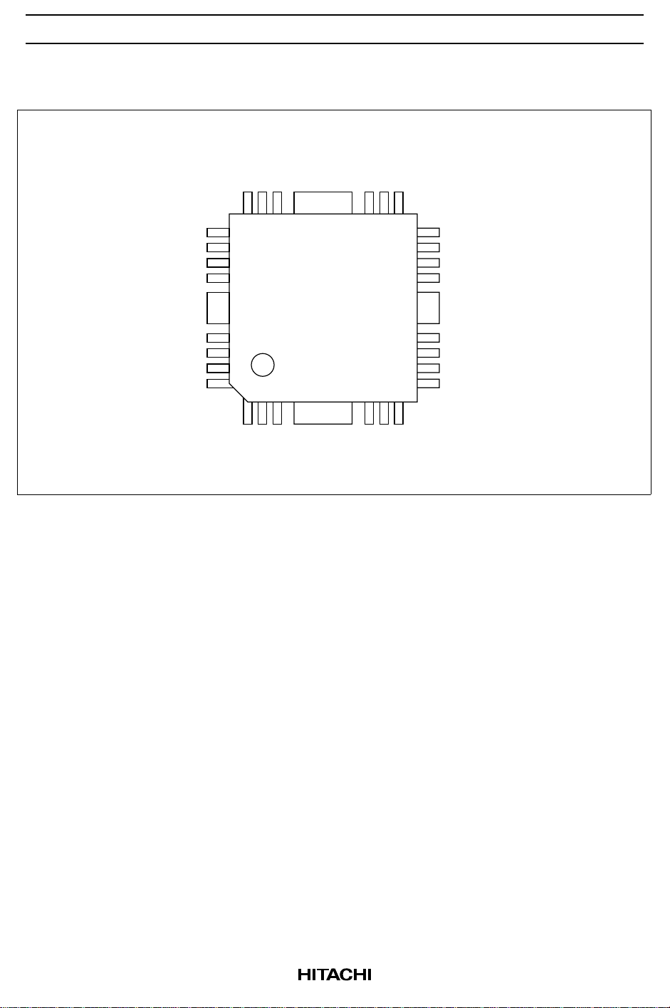
HA13566AF
Pin Arrangement
LVI1
RETOUT
RETPOW
SPNCOMP
VREF2
CDELAY
R
VCMN
VCMP
CT
W
R
NF
PCOMP
18
19
20
21
S
22
23
24
TAB
25
V
26
27
28
123
U
VCMIN
TAB
TAB
CC2
V
(Top view)
16 15
17
TAB
456
VB
BC1
14
13
12
11
10
9
8
7
BC2
DACOUT
POWGOOD
CHAGPMP
DATA
CLK
SERENAB
COMM
PHASE
2
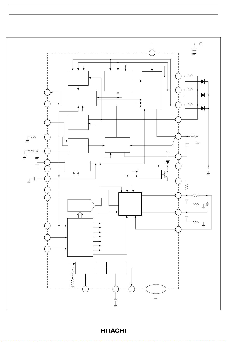
Block Diagram
HA13566AF
V
CC2
3
C101
PHASE
COMM
CHAGPMP
VREF2 (1.25 V)
R1
SPNCOMP
R2
C2
C105
C106
VB
VCMIN
DACOUT
CLK
(10MHz Max)
DATA
SERENAB
C1
12
16
17
14
10
11
B - EMF
Amps
7
8
Commutation
logic
EXTCOM
Center
tap
pull-up
HALF
Charge
pump
5
6
4
SPNENAB
Booster
FBOOST
2
DAC
(9 bit)
Serial port
(11 bit)
9
1.25 V
V
CC2
LVI
Soft
switching
matrix
Current
control
RETRACT
POWGOOD
V
CC2
2
SPNENAB
BRAKE
HALF
EXTCOM
SOFTSW
RETRACT
FBOOST
VCMENAB
POR
delay
SOFTSW
BRAKE
V
CC
VCM
Driver
P
N
Spindle
driver
Retract
U
V
W
V
CC2
D0
VCMP
VCMN
1
26
25
24
27
28
18
19
23
22
21
CT
R
NF
C102
PCOMP
RETPOW
C108
RETOUT
R101
R
C103
R103
C104
R104
RS
D1
D2
D3
S
20 15
CDELAY
LVI1
C107
POWGOOD
3
13
TAB
HA13566AF
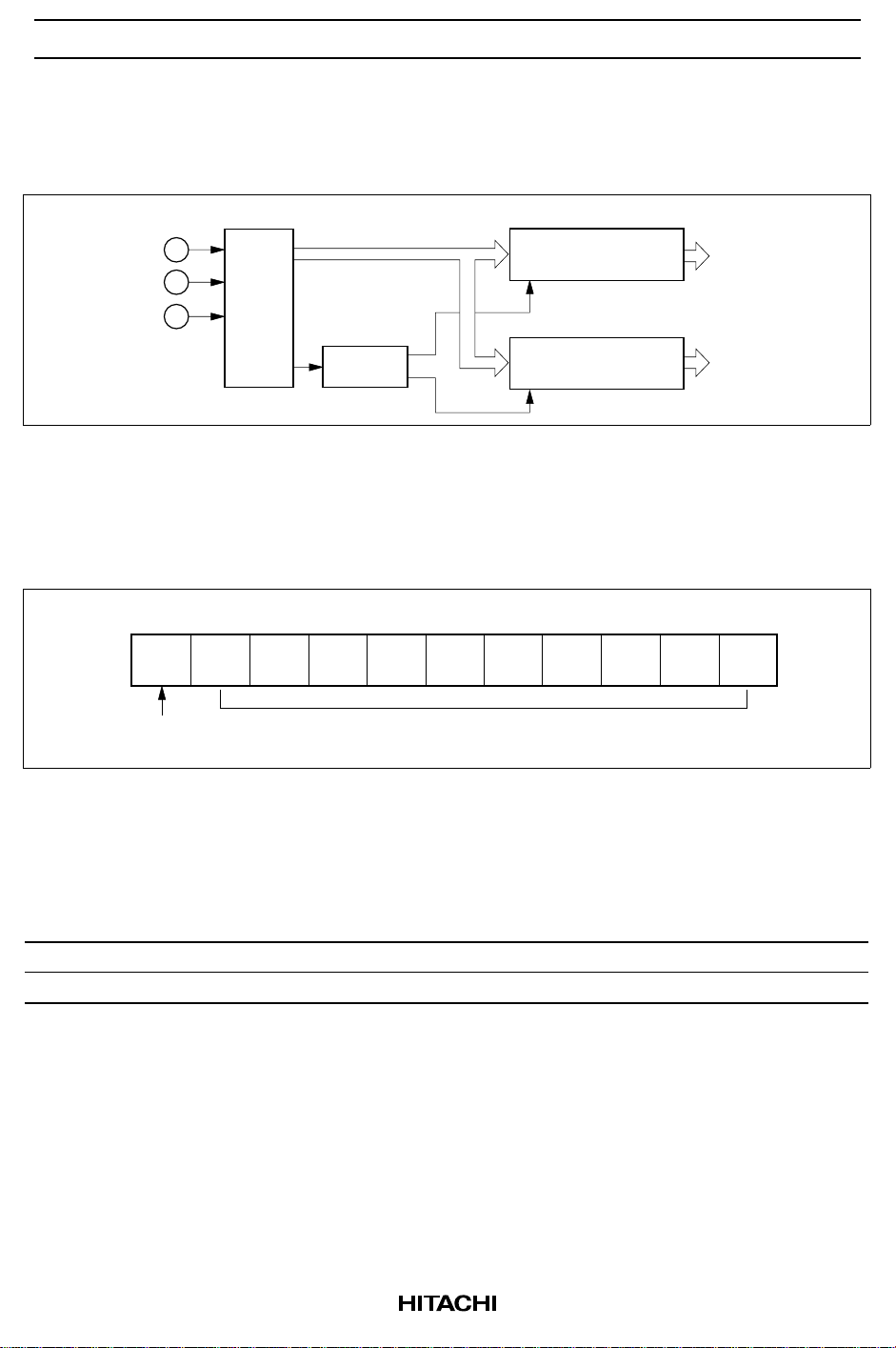
Serial Port
Construction
SERENAB
CLK
DATA
Data construction
Input Data Construction
Serial
port
A0
D0 to D9
Decoder
Figure 1 Serial Port
MD0 to MD9
Mode Control Register
A0 = 1
DD0 to DD9
Input Data Register
for DAC & VCM
A0 = 0
Mode Control
VCM Control
MSB LSB
D9 D8 D7 D6 D5 D4 D3 D2 D1 D0A0
for selecting
register
Register Data
Figure 2 Input Data (1)
The serial port is required the 11 bit data (D0 to D9 and A0). Address bit A0 is used to select the register
as follows. When the data length is less than 11 bits, the internal register will not be up dated. And when
the data length is more than 11 bits, this register will take late 10 bits and ignore the faster bit.
A0 Register
0 Input data register of DAC & VCMGAIN
1 Mode control register
4
HA13566AF
Mode Control Register (A0 = 1)
Bit Symbol 1 0 Note
MD0 SPNENAB Spindle enable Spindle disable 1
MD1 BRAKE Brake enable Brake disable 1
MD2 Not use — —
MD3 HALF Half wave drive Full wave drive
MD4 EXTCOM External commutation Internal commutation 2
MD5 SOFTSW Soft switching Switching
MD6 VCMENAB VCM enable VCM disable
MD7 RETRACT Retracting Not retracting
MD8 POLESEL for 12 poles motor for 8 poles motor 3
MD9 FBOOST Low frequency High frequency 4
Notes: 1. The spindle motor is independently winding to the value of the MD2, during the MD1 is true.
2. The bit MD4 select a commutation mode at driving by B-EMF sensing. (See Commutation
timing)
3. In order to prevent the misdetection of back-EMF amplifier, the bit MD8 should be chosen as
shown above table.
4. The bit MD9 determine the operating frequency of Booster Circuit. According to the frequency of
Input CLK at pin 10, the value of MD9 should be chosen as shown below.
CLK (at pin 10) MD9
7.1 MHz to 10 MHz 0
4.0 MHz to 7.0 MHz 1
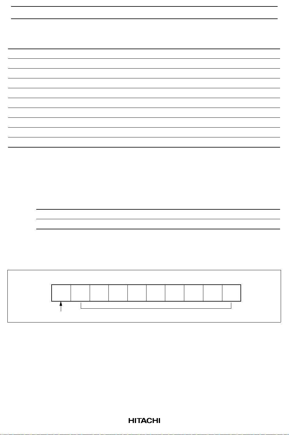
Input Data Register (A0 = 0)
Bit / DD0 to DD9: These input data are used to control the output current at VCM driver as shown follows.
MSB LSB
DD9 DD8 DD7 DD6 DD5 DD4 DD3 DD2 DD1 DD0
VCMGAIN
Input data of DAC
Figure 3 Input Data (2)
5
HA13566AF
The data bit DD9 determine the transfer gain G
which is specified as the relationship between the input
VCM
data at the input data register and the output current at VCM amplifier. (See the under table)
DD9 DATA IO [mA]
1 1FF +199.2/R
S
1 100 0.000
1 000 –200.0/R
0 1FF +24.9/R
S
S
0 100 0.000
0 000 –25.0/R
S
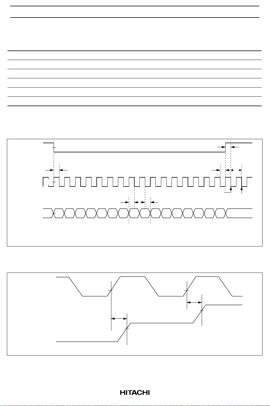
Data Input Timing
SERENAB
CLK
Vth (= 1/2V
t0 t3 t2
Vth
CC2
Typ)
Up date point
t4 t5
t1
Latch point
DATA
Vth
SERENAB
Internal
DAC output
t6 : Conversion time of DAC ≤ 1µs
A0 D9
D8 D7 D6 D5 D4 D3 D2 D1 D0
Figure 4 Input Timing on Serial Port
t6
Figure 5 Conversion Timing on DAC
t0 ≥ 20ns
t1 ≥ 20ns
t2 ≥ 50ns
t6
t3 ≥ 40ns
t4 ≥ 40ns
t5 ≥ 40ns
6
 Loading...