HA13565F
Three-Phase Brushless DC Motor Driver IC
ADE-207-226A (Z)
2nd. Edition
April 1997
Description
HA13565F is a 3-phase brushless DC motor driver IC with digital speed control. It is developed for direct
drive of the spindle motor of 5V floppy disk drives. It has the following functions and features.
Functions
• 3 sensor 1.0A/phase, 3-phase drive circuit
• Digital speed control circuit
• Sensorless index circuit
• Current limiter circuit
• Over-temperature shutdown circuit (OTSD)
• Circuit for switching between 300 and 360rpm speeds
Features
• Low saturation voltage 0.5V Typ (at 0.7A)
• Soft switching drive circuit
• Small surface mount package

HA13565F
Pin Arrangement
CC
U(–)input
U(+)input
V
Hall bias
Bias(–)pin
Bias(+)pin
V(+)input
V(–)input
W(+)input
W(–)input
AGC
NC
NC
FG(+)input
18
19
20
21
22
23
24
TAB
25
26
27
28
123
FG(–)input
RPM control pin
TAB
TAB
Index PC
(Top view)
16 15
17
TAB
456
Index TC
Index output
14
13
12
11
10
9
8
7
CEB
Bias output
U phase output
V phase output
Current detection
W phase output
Phase compensation
Charge pump output
CLK input
2

HA13565F
Pin Function
Pin No. Pin Name Function
1 FG (–) input FG amp. (–) input terminal
2 RPM control pin Control terminal for motor rotation speed
“H” → 360 rpm, “L” → 300 rpm
3 Index PC Connection for the time constant circuit that adjusts the index circuit Vth
level.
4 Index TC Burst setting time constant circuit for index circuit
5 Index output Index signal output terminal (Open collector)
6 CEB Chip enable terminal “H”: disable, “L”: enable
7 CLK input Reference clock input terminal
8 Charge pump output Connection for the time constant circuit that integrates the speed error
signal.
9 Phase compensation Connection for the phase compensation capacitor that stabilizes the
operation of the control system.
10 W phase output W phase output
11 Current detection Output current detection and terminal which is connected with resistor
for current limiter.
12 V phase output V phase output
13 U phase output U phase output
14 Bias output Smoothing circuit for the pumped output circuit
15 Bias (+) pin Output circuit used for bias pumping
16 Bias (–) pin Input circuit used for bias pumping
17 Hall bias Hall element bias input
18 V
19 U phase (+) input U phase (+) input terminal
20 U phase (–) input U phase (–) input terminal
21 V phase (+) input V phase (+) input terminal
22 V phase (–) input V phase (–) input terminal
23 W phase (+) input W phase (+) input terminal
24 W phase (–) input W phase (–) input terminal
25 AGC Smoothing circuit for hall amplifier output amplitude control
26 NC No connection
27 NC No connection
28 FG (–) input Index amp (+) input terminal
CC
Power supply
3

HA13565F
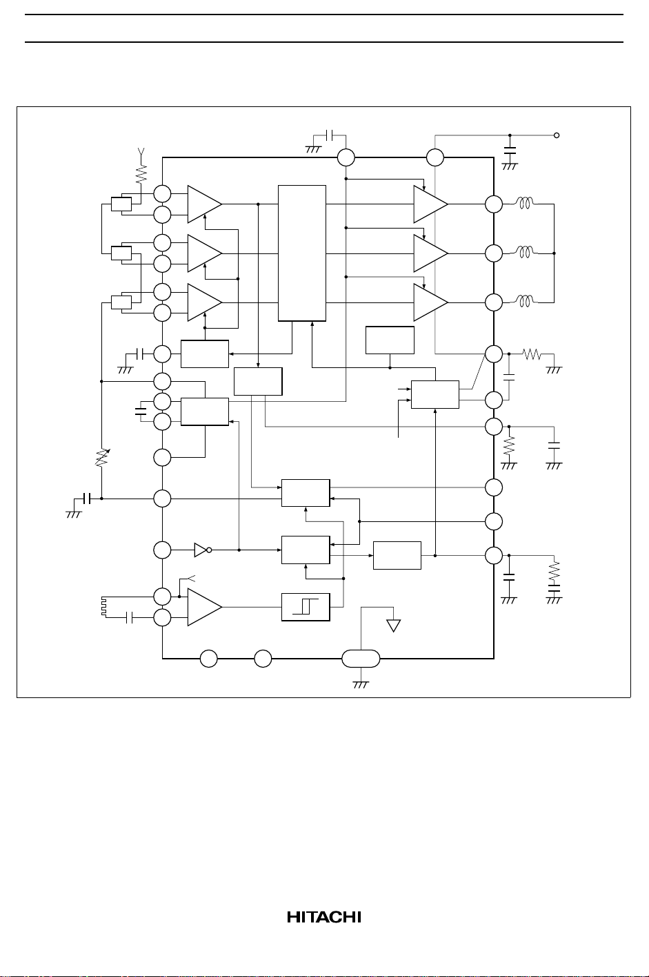
Block Diagram
Rt2
Ct2
FG
60ppr
R101
Hu
Hv
Hw
C104
C103
V
CC
C102
CLK
1MHz
19
20
21
22
23
24
25
17
16
15
28
C105
1814
+
u
–
+
v
–
+
w
–
AGC
Index
detection
Bias
6CEB
4
7
1.6V
+
–
1
FG amp.
Soft
switch
matrix
Time
constant
Discrim-
inator
OTSD
Vref1
0.175V
0.63V
Charge
pump
U
V
W
Current
control
Vref2
C101
13
12
10
11
C106
9
3
5 INDEX output
RPM select
2
H : 360rpm
L : 300rpm
8
C1
Rnf
V
Ct1Rt1
R2
C2
CC
27
NC
26 TAB
NC
4

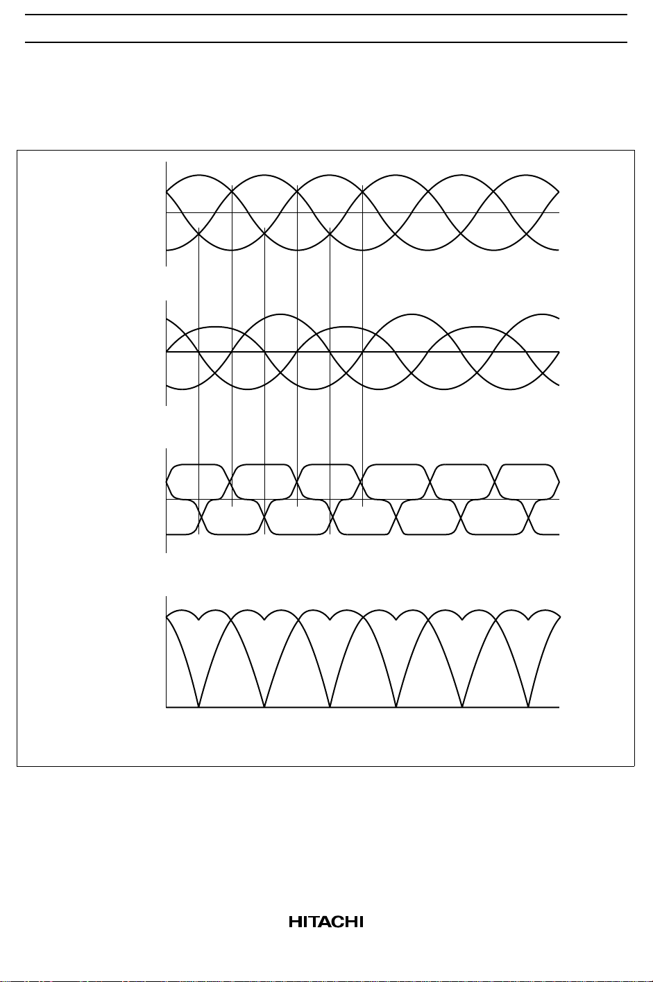
Timing Chart
Hall Amp. Input vs. Output Voltage and Current
HA13565F
B-EMF
Hall amp.
input
Output
current
U
+
0
–
U
+
0
–
UVW
+
0
–
VW
VW
UVW
Output
voltage
0
Note: 1. The input waveforms to the hall amp. should be sine waves with a third harmonic content
of less than 20%.
5

HA13565F
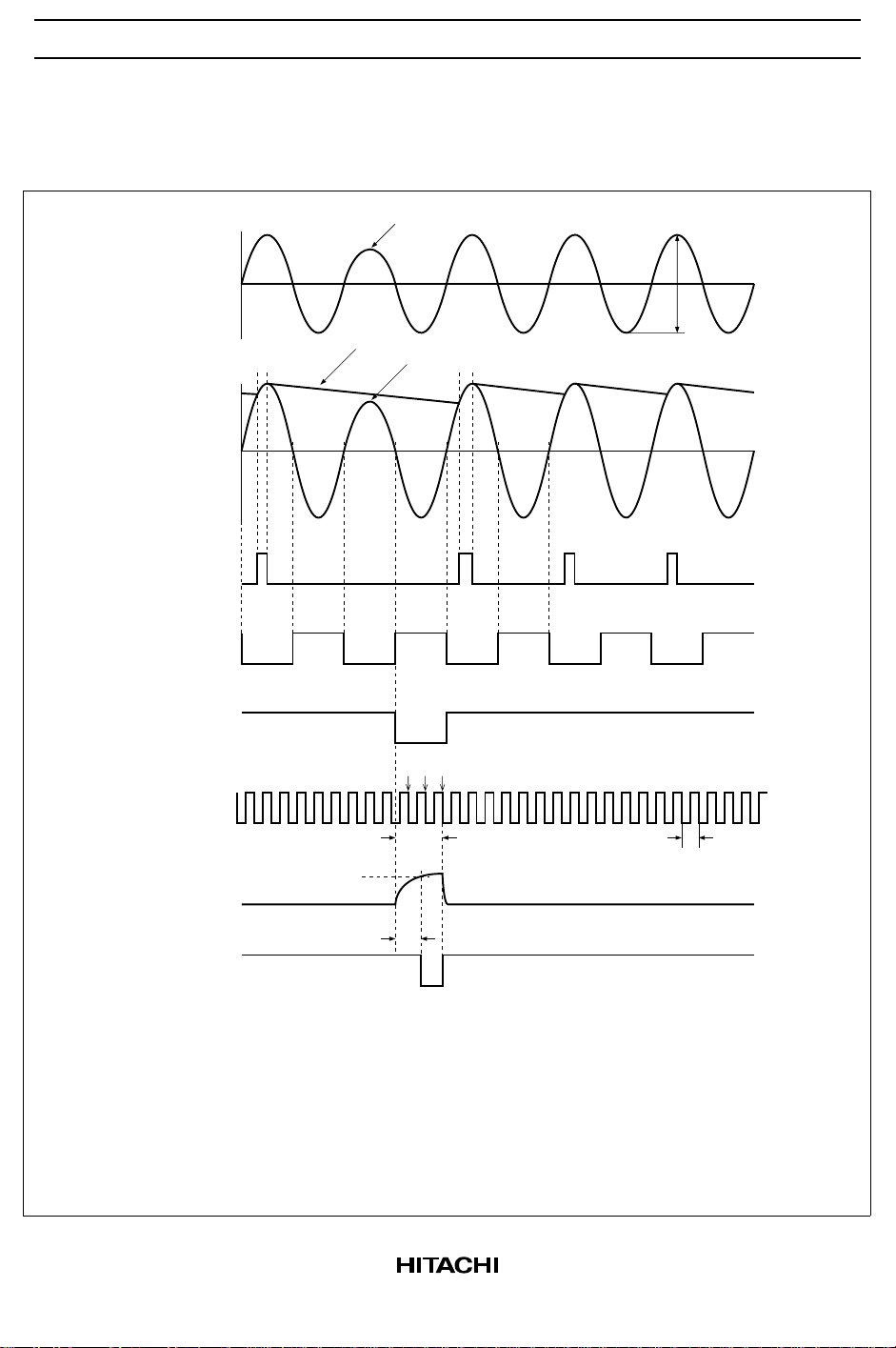
Input Detection Timing
RPM Control Pin = L
U phase hall
amp. input
Pin 19–Pin 20
Index detection
input
Index detection
output-1 *
Index detection
output-2 *
Index detection
output-3 *
2
2
2
Magnetization reduced
by 30% *
1
65 to 200mVpp
+
0
–
Pin 3
Hall amp. output *
2
+
0
–
0
0
0
FG amp.
2
output *
Index TC
Pin 4
0
6.67 to 10ms
(@300rpm) *
3
3.33ms
(@300rpm)
Vth2L
0
Burst adjustment
Index output
Pin 5
Note: 1.
To generate the index output, one pole of the main magnetization must be reduced so that
0
a difference of at least 30% is assured at the Hall amp. input.
These waveforms are shown to indicate the principles of operation, and are not actual
2.
measured waveforms.
Burst adjustment is started by the fall of the index detector output 3, and then, it ends by
3.
the third of fall of FG amp. output.
Incorrect pulses may be output immediately after (i.e., within about 200ms of) start-up.
4.
If the reduction in the magnetization is inadequate, the index signal may not be generated.
5.
Also note that excessive modulation of the Hall amp. input can cause incorrect pulses to be
generated.
6
 Loading...