

Application
UHF local oscillator
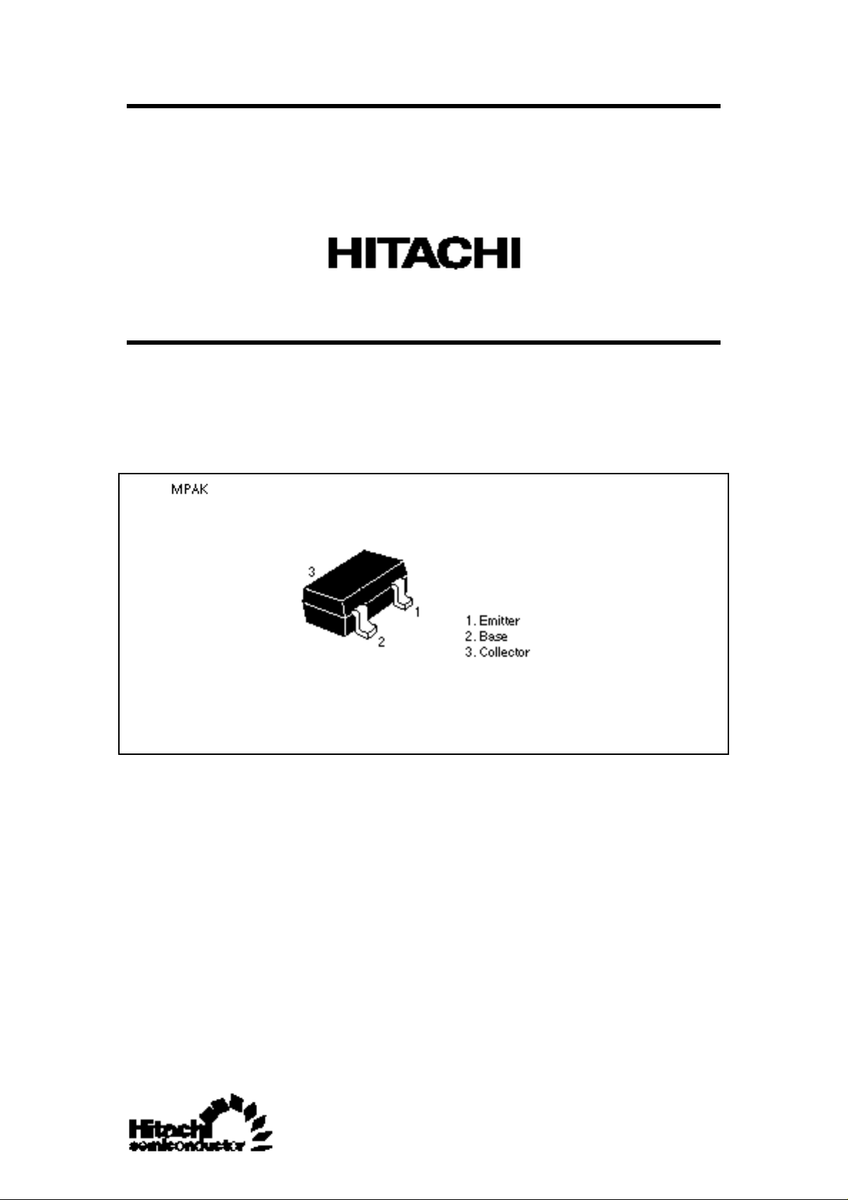
Outline
2SC3793
Silicon NPN Epitaxial
2SC3793
2
Absolute Maximum Ratings (Ta = 25°C)
Item Symbol Ratings Unit
Collector to base voltage V
CBO
20 V
Collector to emitter voltage V
CEO
15 V
Emitter to base voltage V
EBO
3 V
Collector current I
C
50 mA
Collector power dissipation P
C
150 mW
Junction temperature Tj 150 °C
Storage temperature Tstg –55 to +150 °C
Electrical Characteristics (Ta = 25°C)
Item
Symbol Min Typ Max Unit Test conditions
Collector to base breakdown
voltage
Collector to emitter breakdown
voltage
Collector cutoff current I
Emitter cutoff current I
DC current transfer ratio h
Collector to emitter saturation
voltage
Collector output capacitance Cob — 0.7 1 pF VCB = 10 V, IE = 0, f = 1MHz
Gain bandwidth product f
Note: Marking is “IP-”.
V
(BR)CBO
V
(BR)CEO
CBO
EBO
FE
V
CE(sat)
T
20 — — V IC = 10 µA, IE = 0
15 — — V IC = 1 mA, RBE = ∞
— — 1 µA VCB = 15 V, IE = 0
— — 1 µA VEB = 3 V, IC = 0
30 — 200 VCE = 10 V, IC = 5 mA
— — 0.5 V IC = 20 mA, IB = 4 mA
— 2.9 — GHz VCE = 10 V, IC = 5 mA
 Loading...