

Page 1
31
Page 2
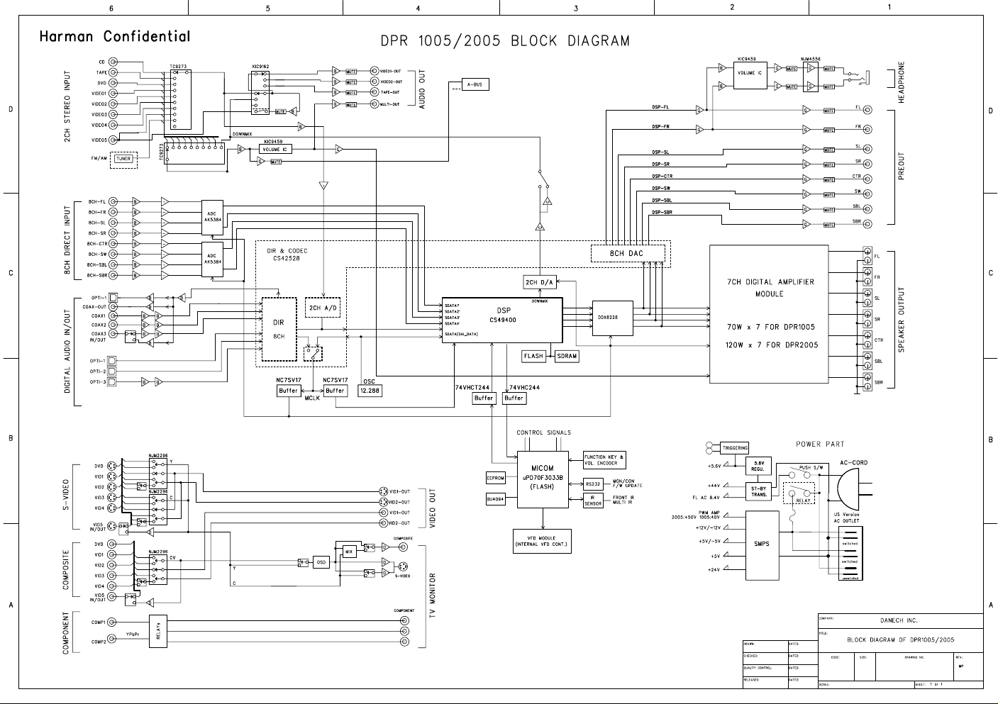
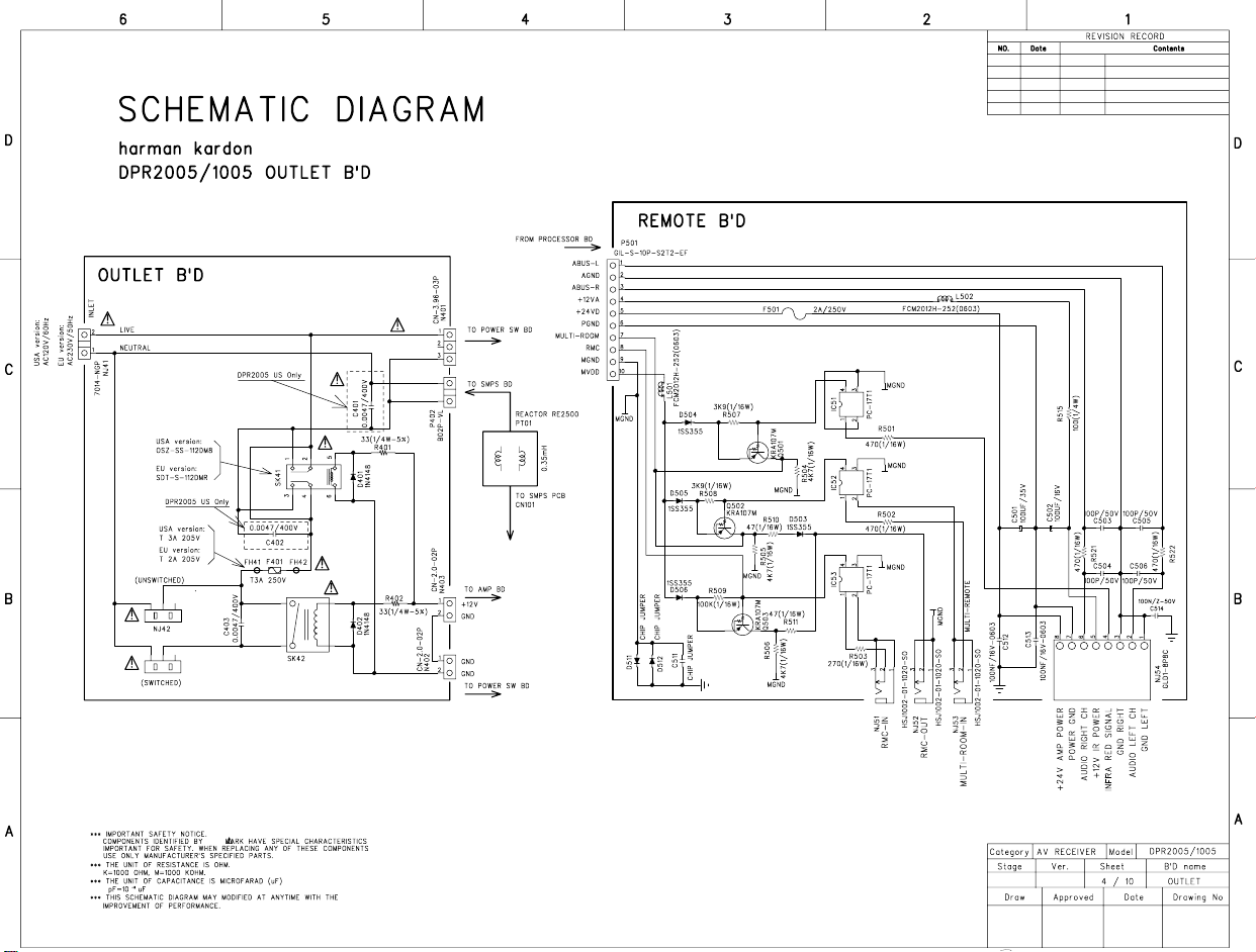
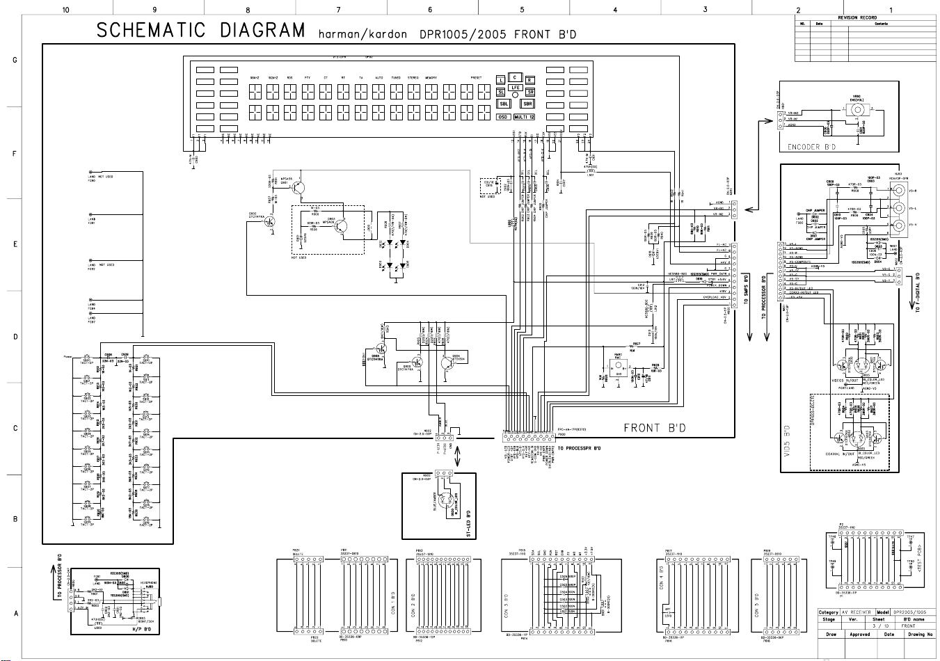
DPR1005/DPR2005 harman/kardon
113
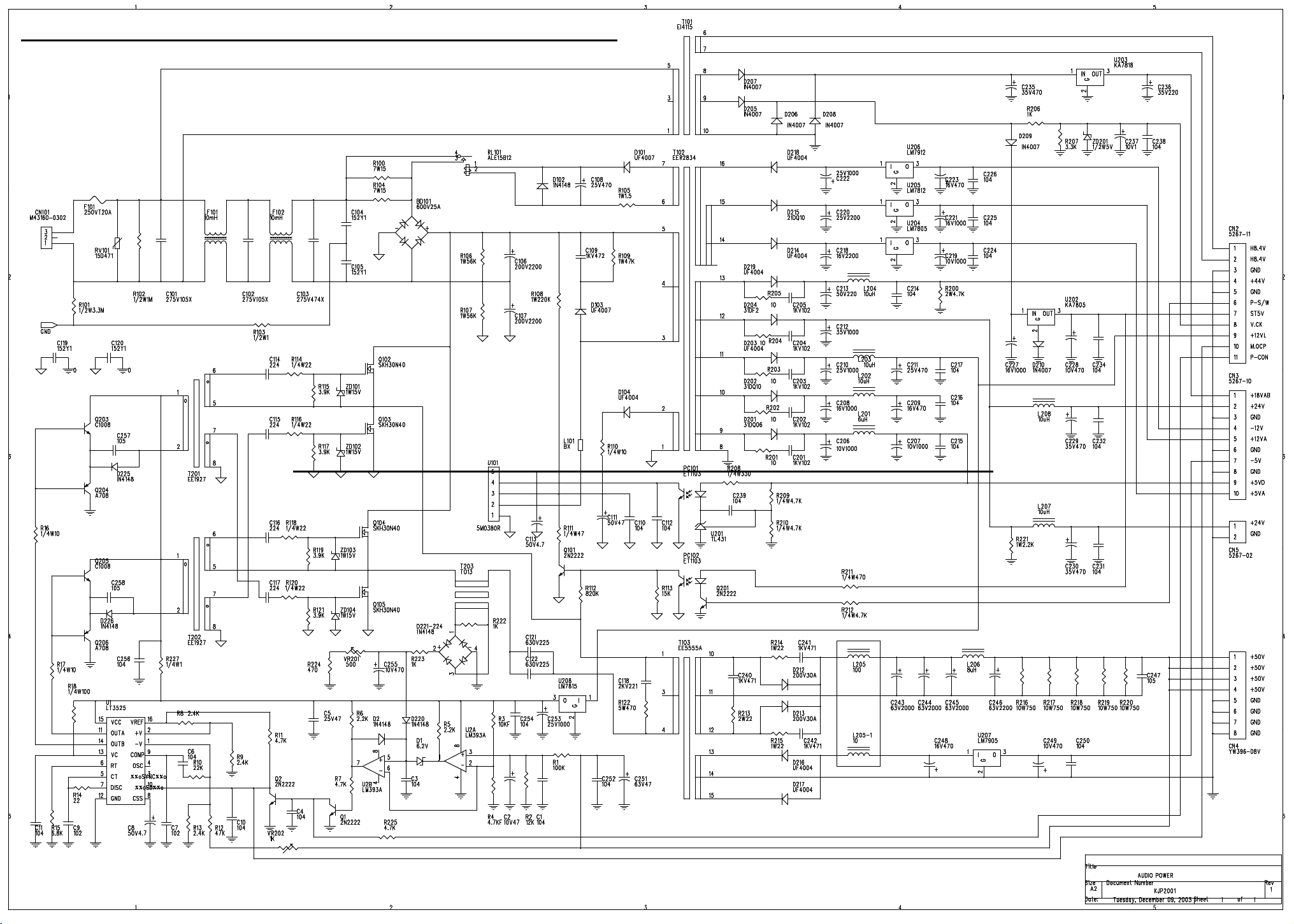
NOTE: Ordinarily the DPR1005/2005 SMPS Power Supply module
is supplied only as a complete unit. Supplied Schematic and Parts list are included only for
reference when the above part is not available and/or repair to component level is necessary.
For h/k part number equivalents, contact harman/kardon at 516-255-4545 ext. 6553
DPR1005/DPR2005 harman/kardon
Page 3
114
Page 4
115
Page 5
116
Page 6
117
Page 7
118
Page 8
119
Page 9
120
Page 10

121
Page 11

122
Page 12

123
Page 13

DPR1005/DPR2005 harman/kardon
124
出 圖
(株)光星電子
Page 14

DPR1005/DPR2005 harman/kardon
125
出 圖
(株)光星電子
Page 15

126
Page 16

DPR1005/DPR2005 harman/kardon
36
GR70 (DPR1005) DATA SHEETS
Complete Class-D Amplifier Module
• Digital switching controller, driver & MOSFET output
stage, output filter stage
• Designed for compliance with FCC, UL, CSA, CE
requirements
High-Performance Sound
• 70 watts per channel into 8 ohms (FTC)
• >96 dB Dynamic Range
• <0.15% THD+N
• 20 Hz to 24 kHz +/-0.5dB frequency response
>90% Efficient
• Internal heat sink
Configurable Audio Processing
• Treble, Bass, Volume Control, and EQ per channel
The D2Audio
channel digital amplifier module. The module enables rapid
system design for manufacturers of home theater
components.
The GR70 contains a high-performance digital switching
controller, MOSFET output stages, and high-quality output
filter stages.
The module is encased in an EMI-shielded package and tested
for compliance with agency regulations to assist FCC Class-B,
UL, CSA, and CE certification.
TM
GR70 is a fully self-contained 70 watts per
• Dynamic range compression and output limiting
• Standard 2-wire serial interface controlled via micro
controller or remote PC GUI
Pure Digital Path
• 8-channel digital audio inputs (32 -192 kHz, 16-24 bit) are
mapped to 7 speaker output channels
Graceful Protection and Recovery
• Short-circuit, thermal, over-current faults
Powered Second Zone
• Dynamic configuration for 7 channels or 5 channels plus
stereo second zone.
• 2-channel analog or independent rate digital input selection
for second zone
A configurable audio signal processor provides equalization,
volume control, tone control, compression, and limiting.
A powered second zone allows for a fully independent
amplifier zone. The amplifier can be dynamically configured
as 7 channels or 5 channels with a stereo second zone. The
second zone supports a stereo analog input or a fully
independent digital audio input.
A separate digital audio output is also provided for the
primary channels.
The GR70 is capable of driving up to 7 channels at 70 watts
into an 8-ohm load with all channels driven per FTC
specifications.
D2AUDIO GR70
• Complete digital amplifier for
home theater components
•70 watts/channel
• Up to 7 channels
• Pure digital audio signal path
• <.15% THD+N, >96dB
dynamic range
• Configurable audio processing
• Powered 2nd Zone
• 90% efficient
• Graceful protection and
recovery
Page 17

DPR1005/DPR2005 harman/kardon
37
3 SPECIFICATIONS
CONSUMER
3.1 ABSOLUTE MAXIMUM RATINGS
Operation at or beyond the Absolute Maximum Ratings may result in permanent damage. Normal operation outside of the limits
defined in this specification is not implied.
Parameter Condition Min Max Unit
High Voltage Supply (HV) +38V DC Supply 40 V
Low Voltage Supply (LV) +12V DC Supply 12.5 V
Signal Voltage Supply (SV) +7.5V DC Supply 8.0 V
MCLK, SCLK,LRCLK,SDI[4:1], Z2_MCLK,
Digital Input Signal Level
Analog Input Signal Level
1
2
Input Current, any pin but supplies +/-10 mA
Operating Temperature Range 0 50 °C
Storage Temperature Range -20 60 °C
Lead Temperature Soldering 10 Seconds 300 °C
Mechanical Shock Any Axis non repetitive TBD G
Mechanical Shock Any Axis Repetitive TBD G
Electrostatic Discharge Machine Model TBD kV
Note 1: -0.6V undershoots and 3.9V overshoots allowed for 4ns maximum
Note 2: Analog inputs are terminated with 10k ohms to analog ground, then AC coupled internally
TABLE 2: Absolute Maximum Ratings
Z2_LRCK, Z2_ SCLK, Z2_SDI, SDA, SCL,
/PWRDWN, /RESET, Z2_EN, Z2_AD,
-0.6 3.90 V
MD0, MD1
Peak to peak AC voltage 5 V
3.2 ELECTRICAL CHARACTERISTICS
TA = 25° C, HV=38V, LV=12V, SV=7.5V, Ground = 0V
Symbol Condition Min Typ Max Unit
V
IL
V
IH
V
IH
V
OH
V
OL
Inputs except /RESET and /PWRDWN 2.0 V
/RESET and /PWRDWN 3.0 V
2 mA Load 2.4 V
2 mA Load 0.4 V
Input Leakage - CMOS pins MCLK, LRCLK,
I
L
SCLK, SDI, Z2_MCLK, Z2_LRCLK,
Z2_SCLK, Z2_SDI
Input current on digital inputs with resistive
I
C
pulls - /PWRDWN, /RESET, Z2_EN,
Z2_AD_EN, MD0, MD1, SDA, SCL
R
I
Z
S
Analog input resistance - all analog audio
inputs
Analog source output impedance 100 Ohms
TABLE 3: Electrical Characteristics
0.8 V
+/-10 uA
+/-0.4 mA
10 k Ohms
GR70 Data Sheet Aug 26, 2003 v1.82
Page 18

D
38
PR1005/DPR2005 harman/kardon
3.3 PERFORMANCE CHARACTERISTICS
Resistance load = 8Ω, HV=38V, LV=12V, SV=7.5V
Specification Condition Min Typ Max Unit
Output Power All channels driven, FTC
3
70 70 W
Frequency Response 20 Hz to 24 kHz, at 1W output power -0.5 0.5 dB
Dynamic Range -60 dB input @ 1kHz -96 dB
Output Distortion (THD+N)
20 Hz to 24 kHz, at 1W output power,
MPC control bit off
0.12 0.15 %
Note 3: FTC spec: 30 minute pre-soak at 1/8th power, full power for 5 minutes, all channels driven simultaneously.
TABLE 4: Performance Characteristics
CONSUMER
3.4 DC POWER REQUIREMENTS
TA = 25°C, HV=38V, LV=12V, SV=7.5V, Ground = 0V
Symbol Description Condition Min Typ Max Unit
4
HV
+12VDC +12V Supply 11.75 12 12.5 V
+7.5VDC +7.5V Supply 7.0 7.5 TBD V
T
srHV
HV High Voltage Supply
+12VDC +12V Supply TBD 1.0 A
+7.5VDC +7.5V Supply TBD 0.85 A
HV High Voltage Supply
+12VDC +12V Supply TBD 1.0 A
+7.5VDC +7.5V Supply TBD 0.85 A
Note 4: The peak current requirement for the HV power supply is dependent on the overall system power output specification.
The GR70 is designed to meet FTC power amplifier specifications for a sine wave continuous power measurement with all channels driven. Under normal conditions for most applications, all channels may not need to be driven at full power simultaneously.
More typically, the power output requirement is 1/8 to 1/3 of the total amplifier output. However, if the amplifier is allowed to
be driven into high distortion (“clipping”), the power supply current may approach 20% more than required for a full scale output. It is therefore up to the system designer to determine how much power output the module will be allowed to produce, and
hence determine the maximum and average power supply current requirements.
TABLE 5: DC Power Requirements
High Voltage Supply 38 V
High Voltage Supply Slew
Rate
See Chapter 5.8 20 V/S
18 TBD A
All channels at full power output
TBD TBD A
/PWRDWN asserted
Primary Digital Audio
Zone 2 Analog
Zone 2 Digital Audio
Zone Control
2-Wire Serial Control
/RESET
/PWRDWN
GR70 Data Sheet Aug 26, 2003 v1.82
ADC
+7.5V Supply
Digital Audio
Out HV Supply
Controller
+12V Supply
Driver 1
Driver 2
Driver 7
Output Protection
/ERROR
Pwr FET 1
Pwr FET 2
Pwr FET 7
GR Module
Filter 1
Filter 2
Filter 7
Speaker
Outputs
1-7
5
Page 19

D
39
PR1005/DPR2005 harman/kardon
3.5 SWITCHING CHARACTERISTICS - SERIAL AUDIO PORT
CONSUMER
TA = 25°C, HV=38V, LV=12V, SV=7.5V, Ground = 0V
Symbol Description Min Typ Max Unit
tcSCLK SCLK frequency 12.5 MHz
twSCLK SCLK pulse width (high and low 40 ns
t
LRCLK LRCLK setup to SCLK rising 20 ns
s
LRCLK LRCLK hold from SCLK rising 20 ns
t
h
t
SDI SDI setup to SCLK rising 20 ns
s
t
SDI SDI hold from SCLK rising 20 ns
h
tdSDO SDO1-4 delay from SCLK falling 20 ns
TAB L E 6: Serial A ud i o Po r t Timing
The second zone inputs Z2_SCLK, Z2_LRCLK and Z2_SDI have the same timing characteristics as the primary serial audio inputs.
The Z2_LRCLK and Z2_SDI input timings are referenced to Z2_SCLK.
SCLK
thLRCLK
LRCLK
SDI
SDO1-4
FIGURE 1: Serial Audio Port Timing
tsLRCLK
tcSCLK
tdSDO
twSCLK
twSCLK
tsSDI
thSDI
GR70 Data Sheet Aug 26, 2003 v1.82
Page 20

D
40
PR1005/DPR2005 harman/kardon
3.6 SWITCHING CHARACTERISTICS - CONTROL PORT
TA = 25°C, HV=38V, LV=12V, SV=7.5V, Ground = 0V
Symbol Description Min Max Unit
fSCL SCL frequency 100 kHz
t
buf
t
SCL SCL clock low 4.7 us
w
t
SCL SCL clock high 4.0 us
w
Bus free time between transmissions 4.7 us
tsSTA Setup time for a (repeated) Start 4.7 us
t
STA Start condition Hold time 4.0 us
h
t
SDA SDA hold from SCL falling (see note) 0 us
h
tsSDA SDA setup time to SCL rising 250 ns
t
SDA SDA delay time from SCL falling 3.5 us
d
t
r
t
f
t
STO Setup time for a Stop condition 4.7 us
s
Rise time of both SDA and SCL 1 us
Fall time of both SDA and SCL 300 ns
Note: Data must be held sufficient time to bridge the 300ns transition time of SCL
t
SDO SDO1-4 delay from SCLK falling 20 ns
d
TAB L E 7: Control Por t T i m ing
CONSUMER
twSCL
SCL
tsSTA
SDA
(input)
SDA
(output)
FIGURE 2: Control Port Timing
thSTA
tsSDA
tdSDA
t
r
thSDA
t
f
tsSTO
t
buf
GR70 Data Sheet Aug 26, 2003 v1.82
7
Page 21

0.01
10
0.02
0.05
0.1
0.2
0.5
1
2
5
%
20 20k50 100 200 500 1k 2k 5k 10k
Hz
DPR1005/DPR2005 harman/kardon
41
3.7 PERFORMANCE PLOTS
CONSUMER
The following graphs show the amplifier’s performance. All inputs are driven with the same input signal, all outputs are mapped to
their respective input with unit gain. The output channels are tested one at a time and only the output channel being measured has a
load. The other outputs are open.
3.7.1 FREQUENCY RESPONSE AT 1W (8Ω LOAD)
Conditions: Typical supplies, Room temperature, 1W output power
+3
+2.75
+2.5
+2.25
+2
+1.75
+1.5
+1.25
+1
+0.75
+0.5
d
+0.25
B
r
-0
-0.25
A
-0.5
-0.75
-1
-1.25
-1.5
-1.75
-2
-2.25
-2.5
-2.75
-3
20 20k50 100 200 500 1k 2k 5k 10k
Hz
FIGURE 3: Frequency Response
3.7.2 THD+N VS. FREQUENCY (8Ω LOAD)
Conditions: Typical supplies, Room temperature, 1W output power
FIGURE 4: THD+N vs. Frequency
GR70 Data Sheet Aug 26, 2003 v1.82
Page 22

DPR1005/DPR2005 harman/kardon
42
3.7.3 THD+N VS. OUTPUT POWER (8Ω LOAD)
Conditions: Typical supplies, Room temperature, 1kHz digital input
0.5
0.48
0.46
0.44
0.42
0.4
0.38
0.36
0.34
0.32
0.3
0.28
0.26
%
0.24
0.22
0.2
0.18
0.16
0.14
0.12
0.1
0.08
0.06
0.04
0.02
100m 100200m 500m 1 2 5 10 20 50
W
CONSUMER
FIGURE 5: THD+N vs. Power
GR70 Data Sheet Aug 26, 2003 v1.82
9
Page 23

D
43
PR1005/DPR2005 harman/kardon
4 MODULE PINOUT
CONSUMER
1
2
3
4
5
6
7
8
9
10
11
12
13
14
15
16
17
18
19
20
21
22
23
24
25
26
27
28
29
30
31
32
33
34
35
36
SCLKO
SDO1
SDO2
SDO3
SDO4
LRCLKO
MCLK
DGND
SCLK
LRCLK
DGND
SDI1
SDI2
SDI3
SDI4
DGND
Z2_MCLK
Z2_SCLK
Z2_LRCLK
Z2_SDI
SDA
SCL
/PWRDWN
/RESET
/ERROR
Z2_EN
DGND
+12V
DGND
+7.5V
Z2_AD_L
Z2_AD_R
AGND
Z2_AD_EN
MD0
MD1
GR70
CH1_OUT+
CH1_OUT-
CH2_OUT+
CH2_OUT-
CH3_OUT+
CH3_OUT-
CH4_OUT+
CH4_OUT-
+40VDC
+40VDC
+40VDC
+40VDC
PWR_GND
PWR_GND
PWR_GND
PWR_GND
CH5/Z2L_OUT+
CH5/Z2L_OUT-
CH6Z2R_OUT+
CH6/Z2R_OUT-
CH7_OUT+
CH7_OUT-
N.C.
N.C.
60
59
58
57
56
55
54
53
52
51
50
49
48
47
46
45
44
43
42
41
40
39
38
37
TOP VIEW
Page 24

DPR1005/DPR2005 harman/kardon
44
4.1 PIN DESCRIPTIONS
Pin # Pin Name I/O Description
1 SCLKO O Output Shift Clock
2SDO1 OChannel 1,2 I
3SDO2 OChannel 3,4 I
4SDO3 OChannel 5,6 I
5SDO4 OChannel 7,8 I
2
S Output Data
2
S Output Data
2
S Output Data
2
S Output Data
6 LRCLKO O Output Left / Right Clock
7 MCLK I Master System Clock
9 SCLK I Serial Data Shift Clock
10 LRCLK I Left / Right Clock
12 SDI1 I Channel 1,2 I
13 SDI2 I Channel 3,4 I
2
S Input Data
2
S Input Data
14 SDI3 I Channel 5,6 I2S Input Data
15 SDI4 I Channel 7,8 I
2
S Input Data
17 Z2_MCLK I Zone 2 Master System Clock
18 Z2_SCLK I Zone 2 Serial Data Shift Clock
19 Z2_LRCLK I Zone 2 Left / Right Clock
20 Z2_SDI I Zone 2 Channel 1,2 I
2
S Input Data
TABLE 8: Digital Signal Pins
CONSUMER
Pin # Pin Name I/O Description
21 SDA I/O 2-Wire Serial Control Interface Data and Address
22 SCL I/O 2-Wire Serial Control Interface Clock
23 /PWRDWN I Amplifier Disable
24 /RESET I Amplifier Internal Reset
25 /ERROR O Amplifier Internal Error
26 Z2_EN I Zone 2 Enable
34 Z2_AD_EN I Zone 2 A/D Enable
35 MD0 I Mode Control Enable 0
36 MD1 I Mode Control Enable 1
TABLE 9: Control Signal Pins
Pin # Pin Name I/O Description
37 NC O No Connection - make no external connection to this pin
38 NC O No Connection - make no external connection to this pin
39 CH7- O Channel 7 Minus Speaker Output
40 CH7+ O Channel 7 Plus Speaker Output
41 CH6/Z2R- O Channel 6 or Zone 2 Right Minus Speaker Output
42 CH6/Z2R+ O Channel 6 or Zone 2 Right Plus Speaker Output
43 CH5/Z2L- O Channel 5 or Zone 2 Left Minus Speaker Output
44 CH5/Z2L+ O Channel 5 or Zone 2 Left Plus Speaker Output
53 CH4- O Channel 4 Minus Speaker Output
54 CH4+ O Channel 4 Plus Speaker Output
55 CH3- O Channel 3 Minus Speaker Output
56 CH3+ O Channel 3 Plus Speaker Output
TAB L E 10: Speak e r O u tput Pins
GR70 Data Sheet Aug 26, 2003 v1.82
11
Page 25

DPR1005/DPR2005 harman/kardon
45
Pin # Pin Name I/O Description
CONSUMER
57 CH2- O Channel 2 Minus Speaker Output
58 CH2+ O Channel 2 Plus Speaker Output
59 CH1- O Channel 1 Minus Speaker Output
60 CH1+ O Channel 1 Plus Speaker Output
TAB L E 10: Speak e r O u tput Pins
Pin # Pin Name I/O Description
8, 11, 16, 27 DGND Digital Ground
45, 46, 47, 48 PWR_GND Output Stage Ground
33 AGND Analog Ground
49, 50, 51, 52 HV +38 VDC High Voltage Power
28 +12VDC +12 VDC Power
30 +7.5VDC +7.5 VDC Power
TABLE 11: Power Supply Pins
Pin # Pin Name I/O Description
31 Z2_AD_L I Zone 2 Analog Left
32 Z2_AD_R I Zone 2 Analog Right
TABLE 12: Analog Inputs
4.2 PIN DEFINITION
4.2.1 ZONE 2 ANALOG INPUTS
Z2_AD_R,L Zone 2 Analog Inputs
This is the Zone 2 analog input. The Z2_AD_R,L are independent analog inputs for the second audio
zone. The inputs are selected when the amplifier is configured for Mode 2 and the Z2_AD input is Set
High. See Chapter 5 for additional information.The A/D convertor is fixed at a 48kHz sample rate with a
2.0V rms input level.
4.2.2 DIGITAL AUDIO INPUTS
MCLK Master System Clock
This pin is the master clock input for the primary channels on SDI[4:1]. The master clock must be an
integer multiple of the LRCLK frequency. The default master clock is 12.288 MHz which corresponds to a
48 kHz sample rate (Fs) * 256. The MCLK is a 3.3 volt input.
LRCLK Left/Right Clock
This pin is the framing clock for the primary channels on SDI[4:1]. The serial input data is transmitted as
two channels every sample rate period. The LRCLK determines the start of each data pair. The LRCLK
frequency determines the input sample rate (Fs). The LRCLK is a 3.3 volt input.
SCLK Shift Clock
This pin is the Shift Clock input for the primary channels on SDI[4:1]. The serial clock is used to frame
each input bit of the serial input data. The shift clock frequency is typically 64*Fs. The SCLK is a 3.3 volt
input.
SDI[4:1] Serial Data Input
These pins are the Serial Data input for the primary channels. Serial Data is arranged as four left/right
inputs. The input format options are I
lengths are available. The SDI pins are 3.3 volt inputs. Note that input channel 8 is not used.
2
S, Left Justified, and Right Justified. 16, 18, 20, and 24 bit data
Channel SDI Input Left or Right
11 Left
TABLE 13: SDI Input to Channel Mapping
GR70 Data Sheet Aug 26, 2003 v1.82
Page 26

DPR1005/DPR2005 harman/kardon
46
21 Right
32 Left
42 Right
53 Left
63 Right
74 Left
84 Right
TABLE 13: SDI Input to Channel Mapping (Continued)
CONSUMER
4.2.3 ZONE 2 DIGITAL INPUTS
Z2_MCLK Zone 2 Master System Clock
This pin is the master clock input for Zone 2. The master clock must be an integer multiple of the
Z2_LRCLK frequency. The default master clock is 12.288 MHz which corresponds to a 48 kHz sample
rate (Fs) * 256. Z2_MCLK is required if the second zone featured is enabled. The Z2_MCLK is a 3.3 volt
input.
Z2_LRCLK Zone 2 Left/Right Clock
This pin is the framing clock of the serial data input for Zone 2. The serial input data is transmitted as two
channels every sample rate period. The Z2_LRCLK determines the start of each data pair. The
Z2_LRCLK frequency determines the input sample rate (Fs).The Z2_LRCLK is a 3.3 volt input.
Z2_SCLK Zone 2 Shift Clock
This pin is the Shift Clock input for Zone 2. The serial clock is used to frame each input bit of the serial
input data. The shift clock frequency is typically 64*Fs. The Z2_SCLK is a 3.3 volt input.
Z2_SDI Zone 2 Serial Data Input
This pin is the Serial Data input for Zone 2. Serial Digital Data is arranged as a single left/right input. The
input format options are I
available. The Z2_SDI is a 3.3 volt input.
2
S, Left Justified, and Right Justified. 16, 18, 20, and 24 bit data lengths are
Channel ZONE 2 SDI Input Left or Right
11 Left
21 Right
TABLE 14: Z2_SDI Input to Channel Mapping
4.2.4 DIGITAL AUDIO OUTPUTS
LRCLKO Output Left/Right Clock
This pin is the framing clock for the serial data for the primary channels on SDO[4:1]. The serial output
data is transmitted as two channels every sample rate period. The LRCLKO determines the start of each
data pair. The LRCLKO frequency determines the input sample rate (Fs).The LRCLKO is a 3.3 volt
output.
SCLKO Output Shift Clock
This pin is the Shift Clock output for the primary channels on SDO[4:1]. The serial clock is used to frame
each input bit of the serial output data. The shift clock frequency is typically 64*Fs. The SCLKO is a 3.3
volt output.
SDO[4:1] Serial Data Output
These pins provide the Serial Data Output for primary Channels. Serial Data is arranged as four left/right
outputs. The SDO is a 3.3 volt output. Note that although input channel 8 does not map to a speaker
output, the results of processing channel 8 may be output on SDO[4].
Channel SDO Outputs Left or Right
11 Left
21 Right
32 Left
TABLE 15: SDO Output to Channel Mapping
GR70 Data Sheet Aug 26, 2003 v1.82
13
Page 27

DPR1005/DPR2005 harman/kardon
47
42 Right
CONSUMER
53 Left
63 Right
74 Left
84 Right
TABLE 15: SDO Output to Channel Mapping
4.2.5 CONTROL INPUTS
SDA Serial Control Data and Address
This pin is the bidirectional Serial Data and Address line for the 2-wire serial control interface. The pin is
pulled internally high to 3.3 volts via a 10 kΩ resistor.
SCL Serial Control Clock
This pin is the bidirectional Serial Clock line of the 2-wire serial control interface. The pin is pulled
internally high to 3.3 volts via a 10 kΩ resistor.
/RESET Reset
This pin is the reset input to the module. Driving the reset to active low for 10 ms will bring all internal
devices to their default state. This is a 3.3 volt input with an internal 10 kΩ resistor to ground. During the
power on sequence, the reset line must be low during the high voltage supply ramp period. It must be held
low for a minimum of 500ms after the supply reaches 95% of its nominal value.
/PWRDWN Amplifier Power Down
This pin is the amplifier power down input. When set high, the amplifier controller is placed in its active
state. When pulled low, the amplifier starts a power down sequence. All outputs are soft muted and the
output stages are disabled. Internal register values are maintained during the power down state. This is a 3.3
volt input with an internal 10 kΩ resistor to ground.
4.2.6 CONTROL OUTPUTS
/ERROR Amplifier Error
The /ERROR signal is an open-collector output with internal 10k ohm pullup to +3.3V. When low,
/ERROR indicates that a fault condition has occurred in the amplifier, or the amplifier is powered down.
Fault conditions include over-temperature, over-current, short circuit, and power output power stage
disabled. When the module is issued a reset, the output stage will be disabled. The error signal will remain
active low until the EAPD (External Amplifier Power Down) bit is set in the appropriate controller
register.
4.2.7 ZONE 2 CONTROL SIGNAL INPUTS
Z2_EN Zone 2 Enable
This pin is the Zone 2 enable. When set active high, the second zone feature is activated. Amplifier
channels five and six are configured as an independent second zone. The second zone input source may be
either the Zone 2 digital I
internal 10 kΩ resistor to ground.
Z2_AD_EN Zone 2 Analog Enable
This pin is the Zone 2 analog input enable. When set active high, the Zone 2 analog input is selected. When
set clear low, the Zone 2 digital I
resistor to ground.
MD[1,0] Mode Configuration
These pins are the Mode access inputs. The Mode access inputs allow the primary and second zone
configuration to be separately controlled. See Chapter 5 for additional detail on the use of the MD1 and
MD0 inputs. The following table describes how the Z2_EN and Mode inputs affect the operating
configuration.
2
S input port or the Zone 2 analog stereo input. This is a 3.3 volt input with an
2
S input port is active. This is a 3.3 volt input with an internal 10 kΩ
Z2_EN MD[1,0] Configuration Access
x 11 Global control access
Table 16: MD Input Control of Configuration Access
GR70 Data Sheet Aug 26, 2003 v1.82
Page 28

DPR1005/DPR2005 harman/kardon
48
Z2_EN MD[1,0] Configuration Access
1 10 Only second zone control
1 01 Only primary zone control
x00Illegal
Table 16: MD Input Control of Configuration Access
CONSUMER
4.2.8 SPEAKER OUTPUTS
CH[7:1]+,- Speaker Channel Outputs
These pins provide the Power Amplifier Outputs. Each channel of the amplifier is a full-bridge output
configuration. Each channel consists of a plus (+) and minus (-) output. The outputs must remain floating
and must not be connected to ground. Amplifier channels may be paralleled for additional power output
into lower impedance speakers. For example two output stages may be paralleled (plus to plus, minus to
minus) to deliver 140 Watts into 4Ω. When paralleled, the plus and minus outputs must never be
connected together or to ground and the input and volume controls must be set correctly.
5 AMPLIFIER OPERATION
5.1 OPERATING MODES
The GR70 amplifier module with the second zone option may be operated in a seven channel configuration or a dual zone
configuration. The dual zone configuration has 5 primary channels and a 2 channel (stereo) second zone. The Z2_EN input selects
the configuration, when high the dual zone operationis selected.
In the seven channel configuration, all seven amplifier outputs are assigned to the primary channels. Zone 2 is disabled. All input
sources are the I
In dual zone configuration, five audio channels are assigned to the primary channels with two channels for the second zone. The
amplifier primary channel outputs are assigned to digital audio inputs, SDI[4,2,1]. Amplifier outputs five and six are assigned as a
second zone, Zone 2. Two audio input sources are available for driving this second zone amplifier output, analog audio inputs
Z2_AD_R,L or the Zone 2 Serial Data input, Z2_SDI. The selection of analog or digital input is controlled by the state of
Z2_AD_EN. When Zone 2 is enabled, input and output channels are mapped to channels five and six. The Zone 2 speaker outputs
are on CH5/Z2L_OUT and CH6/Z2R_OUT.
The primary channels remain on the digital outputs, SDO[4,2,1], but the Zone 2 channels are not available on the digital audio
output.
The following table summarizes the input to output channel mapping.
Z2_EN Z2_AD_EN Primary Input
0 0 SDI[4:1] Disabled Primary Primary
1 0 SDI[4,2,1] Digital Primary Zone 2
1 1 SDI[4,2,1] Analog Primary Zone 2
TABLE 17: Amplifier Channel Mapping
2
S digital inputs (SDI[4:1]). The audio channel data is also available on the digital output port (SDO[4:1]).
Zone 2
Input
Output CH1-4,7 Output CH5,6
5.2 ZONE 2 CONFIGURATION
The MD0 and MD1 inputs provide for independent operation of the speaker outputs when in dual zone configuration. The use of
MD0 and MD1 are configuration register specific and may cause undesirable operation of the GR70 if used outside of the described
procedures. Table 18 lists a definition of terms used in the Zone 2 Configuration.
Ter m
SET High Level Voltage (3.3V) Logic 1
CLEAR(ED) Low Level Voltage (0V) Logic 0
TABLE 18: Definition of Terms
GR70 Data Sheet Aug 26, 2003 v1.82
MD0,MD1,Z2_AD_EN,Z2_EN
Configuration Pins
Control Register
15
Page 29

DPR1005/DPR2005 harman/kardon
49
5.3 ACTIVATING THE AMPLIFIER
CONSUMER
The GR70 does not maintain control register settings when power is off. After reset the GR70 amplifier is in a passive state, all
registers are in their reset state, which results in the outputs being muted.
The following procedure activates the amplifier:
• SET MD0 and MD1
• To activate the output stages, SET the EAPD bit in the ConfF register 05H.
• The MPC bit in ConfA register 00H must be CLEARED for normal operation of the amplifier.
• Configure individual volume controls, mutes, and master volume registers as needed.
• MD0 and MD1 must remain SET for normal amplifier operation.
5.4 POWER DOWN AND POWER OFF
The PowerDown state is the condition where the supplies are at their nominal level, but the amplifier is inactive due to the assertion
or either /RESET or /PWRDWN. Chapters 13.3 through 13.5 describe PowerDown operation. To avoid output pops, the /RESET
input should not be used to transition from the active state to the PowerDown state.
PowerOff is the condition where one or more power supply is off. When transitioning from PowerOff to the condition where all
power supplies are at their nominal level, /RESET should be active. This insures that the amplifier initializes properly with no output
pops. When transitioning from active operation to PowerOff, put it in the PowerDown state or clear the EAPD bit in the ConfF
register 05H. From the PowerDown state (or EAPD low) the power supplies can be turned off without speaker output pops.
5.5 ENABLING ZONE 2
When enabling or disabling the second zone, the following procedure is used:
• SET MD1 and MD0.
• SET master mute bit, MMute, in Mmute register 06H.
• Power down the amplifier output stages, CLEAR EAPD bit in ComfF register 05H.
• CLEAR MD1 and SET Z2_EN.
• If the zone 2 input is analog, enable zone 2 analog input, SET Z2_AD_EN. The input format must also be configured for I
a 48kHz sample rate.
• Configure the digital input format and sample rate using ConfA register 00h and ConfB register 01H. Access to any other registers will
result in undesired operation. The Zone 2 outputs, CH5_OUT and CH6_OUT, are now assigned to input channels Five and Six.
• Program all parameters for zone 2 - EQ, volume, etc.
•SET MD1
• Restore the amplifier output stages: SET EAPD bit in ConfF register 05H and CLEAR the MMute bit in Mmute register 06H.
The amplifier is now ready for operation in the dual zone configuration.
2
S with
5.6 SAMPLE RATE CHANGE WITH ZONE 2 ENABLED
The sample rate of the primary channels may be modified without disturbing the operation of Zone 2. This will be required when
switching between 44.1-48kHz, 96kHz, or 192kHz. Follow this procedure:
• Mute channels 1 through 4 and 7: SET bits C1M through C4M and C7M in Channel Mute register 08H.
•CLEAR MD0.
• Power down the primary amplifier output stages: CLEAR EAPD bit in ConfF register 05H.
• Configure the primary sample rate and digital input format using ConfA register 00h and ConfB register 01H. Access to any other
registers will result in undesired operation.
•SET MD0.
• Restore the amplifier output stages: SET EAPD bit in ConfF register 05H and CLEAR bits C1M through C4M, CM7 in Channel Mute
register 08H.
The amplifier is now ready for operation.
5.7 HEADPHONE OPERATION WITH ZONE 2 ENABLED
The amplifier digital outputs may be used to drive headphones via an external DAC. The speaker outputs of the primary output
channels can be muted for headphone only operation without disturbing the operation of Zone 2. The procedure is:
•CLEAR MD0.
• Power down the primary amplifier output stages, CLEAR EAPD bit in ConfF register 05H.
•SET MD0.
To restore the primary output channels:
•CLEAR MDO
•SET EAPD bit in ConfF register 05H.
Page 30

DPR1005/DPR2005 harman/kardon
50
•SET MDO
5.8 POWER SUPPLY AND POWER ON RESET
During the power on sequence, the reset line must be active during the high voltage supply ramp period. It must be held for a
minimum of 500ms after the supply reaches 95% of its nominal value. The power on rise time of the 46V Power supply MUST NOT
exceed a rise time rate faster than 20V / second. The figure below illustrates the reset timing with power ramp.
High Voltage
Power Supply
POWER SUPPLY RAMP
AND RESET TIMING
.95 Vcc
500MS
2000MS
/RESET
0V
Power ON
500MS
20V / Second Max.
1000MS
1500MS
CONSUMER
5.9 POWER SUPPLY SEQUENCING
Normal device operation expects the high voltage supply to come up first, with the others following as the regulators activate. The
supplies may be turned on and off in any order without harming the amplifier, however the attached speakers may be damaged by
the transients if the amplifier is not muted. Normal device operation expects the the high voltage supply to decay first, then the other
decay as the regulators drop out.
5.10 OPERATIONAL LIMITATIONS
Do not generate audio output greater than 20kHz with no load. Peaking in the output filter can cause the output voltages to exceed
the filter capacitor voltage rating. Normal audio program material will not have enough energy to cause problems. Avoid test tones
above 20kHz.
5.11 AMPLIFIER OVERLOAD PROTECTION
The amplifier monitors drive currents in each power MOSFET and the heat sink temperature. The current sensors protect the
output stage from over-current and short-circuit faults. The temperature sensor protects the amplifier form excessive operating
temperature. The protection features only affect the speaker output stages. The configuration and register settings are not altered by
amplifier protection actions.
Short duration over-current events, such as produced by a loud program passage or momentary speaker terminal short, will cause the
individual output stage to current limit. The /ERROR output will not report a short duration over-current. Longer duration overcurrent events, greater than 250ms, will shut down all speaker output channels and the /ERROR output will be active low. In a dual
zone application, both zones are shut down by a long duration over-current.
Recovery from an over-current shut down is automatic. Approximately 500ms after the over-current shut down, the speaker outputs
will activate. If the condition that caused the shut down persists, the amplifier will shut down in approximately 250ms.
At approximately 100 degress C, the amplifier will shut down all output channels and the /ERROR output will be driven active low
indicating an over-temperature fault. In a dual zone application, both zones are shut down by an over-temperature condition.
Recovery from an over-temperature shut down is automatic. When the amplifier cools to approximately 80 degrees C, the speaker
outputs will activate.
When the amplifier is reset (/RESET input low), or powered down (/PWRDWN low), the /ERROR output will be active low. This
provides an indication that the amplifier is in the reset or power down condition.
GR70 Data Sheet Aug 26, 2003 v1.82
17
 Loading...